JP2012194962A - Coordinate input panel - Google Patents
Coordinate input panel Download PDFInfo
- Publication number
- JP2012194962A JP2012194962A JP2011239019A JP2011239019A JP2012194962A JP 2012194962 A JP2012194962 A JP 2012194962A JP 2011239019 A JP2011239019 A JP 2011239019A JP 2011239019 A JP2011239019 A JP 2011239019A JP 2012194962 A JP2012194962 A JP 2012194962A
- Authority
- JP
- Japan
- Prior art keywords
- conductive segment
- conductive
- coordinate input
- adjacent
- linear
- Prior art date
- Legal status (The legal status is an assumption and is not a legal conclusion. Google has not performed a legal analysis and makes no representation as to the accuracy of the status listed.)
- Granted
Links
Images


Abstract
Description
本発明は、指または座標指示器によりタッチ位置を検出する座標入力システムの、座標入力パネルに関する。 The present invention relates to a coordinate input panel of a coordinate input system that detects a touch position with a finger or a coordinate indicator.
図15は従来の長方形の座標入力領域8を有する座標入力パネル1であり、均一な面抵抗体2に、面抵抗体2と電気的に接続するように、面抵抗体2を取り囲む抵抗性周囲電極3を配設しており、4頂点に検出電極4、5、6、及び7を備えている。検出電極4、5、6、及び7は、抵抗性周囲電極3と電気的に接続されている。座標入力領域8は、面抵抗体2上にあり、抵抗性周囲電極3の内側である。
上記座標入力パネル1を用いた座標入力システムの座標検出方法として、座標入力パネル1が受信側であるような、座標指示器(以下入力ペンとする)から信号を発信し、静電容量結合もしくは面抵抗体2に直接の接触を介して、面抵抗体2が、入力ペンから発信された信号を受信する方法、更には面抵抗体2全体を電圧振動させて、指又は導電物で指示した点の位置を入力パネル側で検出する方法、及び、信号伝達の方向がこれと逆であって、座標入力パネル1が発信側であるような、面抵抗体2の各部を信号駆動し、入力ペンで座標信号を受信する方法がある。
座標入力パネル1が受信側である場合は、面抵抗体2の一点に出入りする電流の、4頂点(4、5、6、及び7)へ配分される電流値を計測するものが知られている{特許3237629号(特許文献1)参照}。一方、座標入力パネル1が発信側である場合は、面抵抗体2に、検出電極4、5、6、及び7を通じて外部から電位勾配を与え、入力ペンによって指示座標点の電圧レベルを検出するものが知られている。指や入力ペンで指示した位置の座標は、面抵抗体2に出入りする電流の4頂点への配分値、もしくは4頂点を駆動した際に入力ペンで計測した電圧を用いて、計算される。また、座標入力パネル1の座標入力領域8が長方形ではなく、一般的な多角形である場合についての座標検出方法としては、例えば同一出願人による特開2010−86088号(特許文献2)が存在する。
上述した座標入力システムにおいて、指または導電物(座標入力指示器、例えば、入力ペン)が面抵抗体に近接または接触した点の位置を正確に検出するためには、座標入力領域8内に生じる電位分布あるいは電流分布を均一にすることが必要となる。抵抗性周囲電極3の辺あたりの抵抗値、もしくは長さあたりの抵抗率が高いと、接触した点の位置検出がずれることが分かっている。このため座標入力パネルを設計する場合、抵抗性周囲電極3の抵抗値は、面抵抗体2の抵抗値に対してできるだけ低いことが好ましい。しかしながら、抵抗性周囲電極3の抵抗値を低く設定しすぎると、消費電力が大きくなったり、電位勾配を与える駆動電流が大きく、面抵抗体2にDCまたはACの電位勾配を強制的に作ることができなくなるなどの、回路制御上の不都合が生じる。一方、逆に面抵抗体2の抵抗値を高くすれば、抵抗性周囲電極3の抵抗値を相対的に下げることができるが、面抵抗体2の抵抗値を上げると、ノイズに弱くなるといった問題があった。従って、抵抗性周囲電極3は、適切な抵抗値を設定することが望まれる。
抵抗性周囲電極3の抵抗値を適切な値にするためには、例えば、一定の抵抗率を持った物質を直線的に塗布し、抵抗性周囲電極3の各辺と成す、という方法がある。この方法により作成された抵抗性周囲電極の一辺あたりの抵抗は長さに対して直線的である。ただし、塗布する物質として、例えば銀を用いると、銀の抵抗率が低いため、適切な値の抵抗値にするためには抵抗性周囲電極3の各辺を極めて細い幅にしなくてはならず、形成方法が難しい。また、銀にカーボンを混合して抵抗値を高くしたものは、周囲電極形成に適しているが、異なった材料を混合する必要があり、製造工程上、安定した抵抗値を維持するのが困難である。また、パネル個々の面抵抗が異なると抵抗性周囲電極3の抵抗値の設計を再検討する必要があった。
また抵抗性周囲電極3を形成する別の方法として、抵抗の低い導電性物質(たとえば銀インク)のセグメントを使用して非連続パターンを形成し、間隙に存在する面抵抗体2の抵抗により、所定の抵抗値を実現するものがある(例えば、特表2005−530274号(特許文献3)または、特願2009−271693(特許文献4)参照)。これらの方法では、電位分布あるいは電流分布を均一にするための導電性セグメントの配列パターンが複雑、または、抵抗性周囲電極の面積が座標入力パネル全体の面積に占める割合に対して高くなってしまうことが多く、抵抗性周囲電極3の抵抗値の設計が困難になることがあった。
さらに、座標入力パネル1の製造方法は、有機もしくは無機材料からなる透明基材に面抵抗体2を被覆し、その上に抵抗性周囲電極3を形成する。
その際、面抵抗体2の被覆方法によってはパネル毎に抵抗値のばらつきがあることがあり、抵抗性周囲電極3をパネル毎に、抵抗調整を必要とすることがあった。
FIG. 15 shows a conventional
As a coordinate detection method of the coordinate input system using the
When the
In the coordinate input system described above, in order to accurately detect the position of a point where a finger or a conductive material (coordinate input indicator, for example, an input pen) is close to or in contact with the surface resistor, it occurs in the coordinate input area 8. It is necessary to make the potential distribution or current distribution uniform. It is known that when the resistance value per side of the resistive surrounding
In order to set the resistance value of the resistive surrounding
Another method for forming the resistive surrounding
Furthermore, the manufacturing method of the
At that time, depending on the coating method of the
本発明はこのような点を考慮してなされたものであり、抵抗性周囲電極の材料として、材料の混合などの必要がない単一の導電性材料を使用でき、抵抗性周囲電極の抵抗値の設計を容易に実施することができ、且つ、パネル毎における面抵抗のばらつきによる座標検出調整をなくす抵抗性周囲電極のパターンを持つ座標入力パネルを提供することを目的とする。 The present invention has been made in consideration of such points, and a single conductive material that does not require mixing of materials can be used as the material of the resistive surrounding electrode, and the resistance value of the resistive surrounding electrode can be used. It is an object of the present invention to provide a coordinate input panel having a pattern of resistive surrounding electrodes that can easily implement the above design and eliminates coordinate detection adjustment due to variations in sheet resistance for each panel.
本発明は、面抵抗体と、該面抵抗体の上に形成された略直線状の少なくとも3本以上の抵抗性周囲電極から成り、前記抵抗性周囲電極の端部は、検出電極により互いに電気的に接続され、前記検出電極を角部頂点とし、前記少なくとも3本以上の抵抗性周囲電極で取り囲まれた部分を座標入力領域とする座標入力パネルであって、面抵抗体に対して内側に配列された第一の導電性セグメントは、交互に同じ長さの直線状の導電性セグメントが破線状に並んでおり、第二の導電性セグメントが前記第一の直線状の導電性セグメントの面抵抗体に対して外側に設けた少なくとも2段以上の階段状の形状を成し、且つ、前記少なくとも2段以上の階段形状を成した導電性セグメントは、各階段形状を成した導電性セグメント同士が、互いに近接し平行に配置され、隣り合う階段形状の導電性セグメントのそれぞれ異なる段同士が、近接して隣り合う箇所を少なくとも1箇所以上有し、前記第二の階段形状の導電性セグメントの最も内側の段の中央に1本の前記第一の直線状の導電性セグメントが隣接し、該直線状の導電性セグメントの両側に位置する各第一の直線状の導電性セグメントが、前記第二の階段形状の導電性セグメントの最も内側の段と、前記階段形状の導電性セグメントの両側に位置する前記第二の階段形状の導電性セグメントの最も内側の段をまたぐように、近接して配置したものであって、少なくとも2段以上の前記の第二の導電性セグメントである階段形状を成した導電性セグメントは、各階段形状を成した導電性セグメント同士が、互いに近接し平行に配され、隣り合う階段形状の導電性セグメントのそれぞれ異なる段同士が、近接して隣り合う箇所を少なくとも1箇所以上有するパターンの抵抗性周囲電極を設けたことを特徴とする座標入力パネルを第一の要旨とし、面抵抗体と、該面抵抗体の上に形成された略直線状の少なくとも3本以上の抵抗性周囲電極から成り、前記抵抗性周囲電極の端部は、検出電極により互いに電気的に接続され、前記検出電極を角部頂点とし、前記少なくとも3本以上の抵抗性周囲電極で取り囲まれた部分を座標入力領域とする座標入力パネルであって、面抵抗体に対して内側に配列された第一の導電性セグメントは、同じ長さの第一の直線状の導電性セグメントが破線状に並んでおり、第二の導電性セグメントが前記第一の直線状の導電性セグメントの面抵抗体に対して外側に設けた少なくとも2段以上の階段状の形状を成し、且つ、前記少なくとも2段以上の階段形状を成した導電性セグメントは、各階段形状を成した導電性セグメント同士が、互いに近接し平行に配置され、隣り合う階段形状の導電性セグメントのそれぞれ異なる段同士が、近接して隣り合う箇所を少なくとも1箇所以上有し、前記第一の直線状の導電性セグメントが、前記第二の階段形状の導電性セグメントの最も内側の段と、前記階段形状の導電性セグメントの両側に位置する前記階段形状の導電性セグメントの最も内側の段をまたぐように、近接して配置したものであって、少なくとも2段以上の前記第二の階段形状を成した導電性セグメントは、各階段形状を成した導電性セグメント同士が、互いに近接し平行に配置され、隣り合う階段形状の導電性セグメントのそれぞれ異なる段同士が、近接して隣り合う箇所を少なくとも1箇所以上有するパターンの抵抗性周囲電極を設けたことを特徴とする座標入力パネルを第二の要旨とし、第一の直線状の導電性セグメントの外側に設けた第二の階段状のセグメントは少なくとも2段以上を成した導電性セグメントが並んだものと、前記面抵抗体のうち、前記破線状に並んだ前記第一の直線状の導電性セグメントと前記並んだ階段形状の導電性セグメントに囲まれた領域から成り、面抵抗体を取り囲む様に設けた抵抗性周囲電極を構成する少なくとも2段以上の階段形状を成した導電性セグメントのパターンが、各抵抗性周囲電極の中心で線対称であり、各階段形状を成した導電性セグメント同士が、互いに近接し平行に配され、隣り合う階段形状の導電性セグメントのそれぞれ異なる段同士が、近接して隣り合う箇所を少なくとも2箇所以上有するパターンの抵抗性周囲電極を設けたことを特徴とする請求項1及び2記載の座標入力パネルを第三の要旨とし、検出電極に電気的に接続される抵抗性周囲電極の端部は、前記検出電極近傍を抵抗性周囲電極の端部として終了させ、第一の直線状の導電性セグメントは、検出電極と間隙を持ち、且つ、少なくとも第一の直線状の導電性セグメントに最も近い第二の階段状の導電性セグメントの終了端部は、検出電極に直接接続されていることを特徴とする請求項1〜3記載の座標入力パネルを第四の要旨とし、面抵抗体と、該面抵抗体の上に形成された略直線状の少なくとも4本以上の抵抗性周囲電極から成り、第二の階段形状の導電性セグメントのパターンが、第一の直線状の導電性セグメントに隣接する第一段と、第二段間の重なりあう間隔が、第二段と第三段間が重なり合う間隔よりも広いパターンとした抵抗性周囲電極を設けたことを特徴とする請求項1〜3記載の座標入力パネルを第五の要旨とする。
The present invention includes a surface resistor and at least three or more substantially linear resistive surrounding electrodes formed on the surface resistor, and the ends of the resistive surrounding electrodes are electrically connected to each other by a detection electrode. A coordinate input panel in which the detection electrode is a corner apex, and a portion surrounded by the at least three resistive surrounding electrodes is a coordinate input region, and is located inside the surface resistor In the arranged first conductive segments, linear conductive segments of the same length are alternately arranged in a broken line, and the second conductive segment is a surface of the first linear conductive segment. The conductive segments having at least two steps or more provided outside the resistor and having the at least two steps or more are conductive segments having the respective steps. But close to each other and flat Each of the different steps of the adjacent staircase-shaped conductive segments adjacent to each other has at least one adjacent and adjacent center, and the center of the innermost step of the second staircase-shaped conductive segment. The first linear conductive segment is adjacent to the first linear conductive segment, and the first linear conductive segments located on both sides of the linear conductive segment are connected to the second step-shaped conductive segment. Adjacent to the innermost step of the conductive segment and the innermost step of the second step-shaped conductive segment located on both sides of the step-shaped conductive segment. The conductive segments having the staircase shape, which is the second conductive segment having at least two steps, are arranged so that the conductive segments having the staircase shapes are adjacent to each other and arranged in parallel. A coordinate input panel characterized in that a resistive peripheral electrode having a pattern having at least one place adjacent to each other in adjacent steps of the step-shaped conductive segment is provided as a first gist. It consists of a surface resistor and at least three or more substantially linear resistive surrounding electrodes formed on the surface resistor, and the ends of the resistive surrounding electrodes are electrically connected to each other by a detection electrode. A coordinate input panel having the detection electrode as a corner vertex and a portion surrounded by the at least three or more resistive surrounding electrodes as a coordinate input region, and arranged inward with respect to the surface resistor. In one conductive segment, first linear conductive segments having the same length are arranged in a broken line, and the second conductive segment is a sheet resistor of the first linear conductive segment. Against The conductive segments having a staircase shape of at least two steps provided on the side and having the staircase shape of at least two steps are adjacent to each other. The different steps of the adjacent step-shaped conductive segments arranged in parallel have at least one location adjacent to each other, and the first linear conductive segment is the second linear conductive segment. The staircase-shaped conductive segment is disposed adjacent to each other so as to straddle the innermost step of the staircase-shaped conductive segment and the innermost step of the staircase-shaped conductive segment located on both sides of the staircase-shaped conductive segment. In addition, the conductive segments having the second staircase shape having at least two steps are adjacent to each other in such a manner that the conductive segments having the respective staircase shapes are arranged close to each other in parallel. A second aspect of the coordinate input panel is characterized in that a resistive peripheral electrode having a pattern having at least one location adjacent to each other in adjacent steps of the step-shaped conductive segment is provided. The second step-like segment provided outside the one linear conductive segment is one in which at least two or more conductive segments are arranged, and the line resistor is arranged in the broken line shape among the surface resistors. The first linear conductive segment and the region surrounded by the stepwise conductive segments arranged side by side, and comprising at least two or more steps constituting a resistive peripheral electrode provided so as to surround the surface resistor The shape of the conductive segments formed in the shape is line symmetric at the center of each resistive surrounding electrode, and the conductive segments formed in the respective step shapes are arranged close to each other in parallel, The coordinate input according to
本発明による座標入力パネルによれば、抵抗性周囲電極の材料として、単一の導電性材料を使用することができるので、抵抗性周囲電極の抵抗値を安定させることができ、製造工程における歩留まりを上げることができる。また、抵抗性周囲電極の材料として低抵抗の銀を用いれば、検出電極と同じ材料を使用することができるので、印刷などによって検出電極と抵抗性周囲電極を同時に形成することができ、両者を別々に形成するよりもコストを下げることが可能になる。
また、座標入力パネルの寸法が変更になった場合、従来は、抵抗性周囲電極の一辺あたりの抵抗値を変更する必要があったが、パターンの拡大収縮もしくは階段状セグメントの段数の増減により簡単に抵抗値を調整でき、従来の抵抗性周囲電極より面積を小さくすることが可能となる。
また、面抵抗体をそのまま抵抗性周囲電極の一部として組み入れているため、面抵抗体の製造時におけるパネル毎の抵抗値のばらつきを補償するような抵抗性周囲電極を形成することができ、面抵抗のばらつきによる抵抗値調整をなくすことが可能である。
According to the coordinate input panel of the present invention, since a single conductive material can be used as the material of the resistive surrounding electrode, the resistance value of the resistive surrounding electrode can be stabilized, and the yield in the manufacturing process can be stabilized. Can be raised. In addition, if low resistance silver is used as the material for the resistive surrounding electrode, the same material as the sensing electrode can be used, so the sensing electrode and the resistive surrounding electrode can be formed simultaneously by printing or the like. Costs can be reduced as compared with separate formation.
In addition, when the dimensions of the coordinate input panel are changed, it has been necessary to change the resistance value per side of the resistive surrounding electrode, but this can be easily done by expanding / shrinking the pattern or increasing / decreasing the number of steps in the stepped segment. Thus, the resistance value can be adjusted, and the area can be made smaller than that of the conventional resistive surrounding electrode.
In addition, since the surface resistor is incorporated as a part of the resistive peripheral electrode as it is, it is possible to form a resistive peripheral electrode that compensates for variations in resistance value for each panel during the manufacture of the surface resistor. It is possible to eliminate resistance value adjustment due to variations in sheet resistance.
以下、添付図面に従って、本発明に係る座標入力パネルの好ましい実施の形態について詳述する。
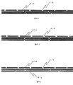
図2は本発明になる多角形の座標入力パネル11の概略図である(図2には4角形の例を示す)。座標入力パネル11は、基材(図示せず)の上に、均一な面抵抗体12を形成し、面抵抗体12と電気的に接続するように、面抵抗体12を取り囲む抵抗性周囲電極13を形成し、更に、各頂点に検出電極14、15、16、及び17を形成したものである。抵抗性周囲電極13は、複数の細長い第一の直線状の導電性セグメント41aと、直線を組み合わせた階段状の導電性セグメント41bから成り、面抵抗体12と、互いに隣り合う導電性セグメントの間隙を成す部分との集合体から成る。座標入力領域18は、抵抗性周囲電極13の内側の領域を指す。
座標入力パネル11の基材(図示せず)は、例えば、ソーダガラスを使用することができるが、特に材質が限定されるものではなく、任意のガラスを含む透明なセラミックス素材、あるいはアクリル樹脂、ポリエチレンテレフタレート樹脂などの透明な樹脂素材を使用できる。用途によっては不透明な絶縁性の基材を用いてもよい。
座標入力パネル11の基材(図示せず)を被覆する面抵抗体12の導電性薄膜の材料としては、一般に、酸化錫、アンチモンを添加した酸化錫(ATO)、酸化インジウム、錫を添加した酸化インジウム(ITO)、亜鉛を添加した酸化インジウム(IZO)、酸化亜鉛等が用いられる。また、被覆方法としては、例えば、物理的方法のスパッタリング法、真空蒸着法、イオンプレーティング法、また、化学的方法のスプレー法、ディップ法、化学気相成長法(CVD法)がある。
抵抗性周囲電極13を構成する導電性セグメントは、例えば銀や金といった貴金属や銅、錫、ニッケルといった金属の単一金属微粒子を分散させた低抵抗の導電性インクを用い、スプレー法、インクジェット法、スクリーン法、ディスペンサ法等といった手法によりパターンを形成した後に、焼成して形成する方法や、前記金属をめっきによりパターン形成する方法がある。各頂点の検出電極14〜17は、引き出し線22、23、24、25を接続するためのものであり、線材であればハンダ付け可能な導電性インクを印刷・焼成して形成するか、フレキシブルケーブル(FFCまたはFPC)であれば、導電性接着剤もしくは導電性フィルム等で接着し形成する。検出電極14〜17を形成するための導電性インクの場合、抵抗性周囲電極13を構成する導電性セグメントを形成するのと同じものを使用することができるため、検出電極14〜17と、抵抗性周囲電極13を構成する導電性セグメントは、一回の処理で印刷・焼成して形成することが可能である。
更に、図示しないが、指または座標指示器と面抵抗体12との相互作用に容量結合を用いる場合は、面抵抗体12を保護するために、面抵抗体12上に、透明絶縁性基材を被覆してもよい。
Hereinafter, preferred embodiments of a coordinate input panel according to the present invention will be described in detail with reference to the accompanying drawings.
FIG. 2 is a schematic view of a polygonal coordinate input panel 11 according to the present invention (FIG. 2 shows an example of a quadrangle). The coordinate input panel 11 forms a
As the base material (not shown) of the coordinate input panel 11, for example, soda glass can be used, but the material is not particularly limited, and a transparent ceramic material containing arbitrary glass, or an acrylic resin, Transparent resin materials such as polyethylene terephthalate resin can be used. Depending on the application, an opaque insulating substrate may be used.
In general, tin oxide, tin oxide added with antimony (ATO), indium oxide, and tin are added as materials of the conductive thin film of the
The conductive segment that constitutes the resistive surrounding
Further, although not shown, when capacitive coupling is used for interaction between the finger or the coordinate indicator and the
図3は、本発明の座標入力パネル11を用いた座標入力システムの一例を示す構成図であり、座標入力パネル11が受信側である場合である。指21が座標入力パネル11の座標入力領域18内で指示した位置座標を検出する座標入力システムの構成図である。面抵抗体12の表面は、前記したように、指21が面抵抗体12に直接触れない様に絶縁処理することによって、指21と面抵抗体12との静電容量結合による信号伝達をさせるようにしてもよいし、絶縁処理せず、指21と面抵抗体12の直接的な電気的接触による信号伝達をさせるようにしてもよい。ここでは、面抵抗体12の表面に、透明絶縁性基材を被覆して絶縁処理をした場合を説明する。均一な面抵抗体12上に、各辺が図2aに示すパターンを用いた抵抗性周囲電極13を形成し、抵抗性周囲電極13で囲まれた内部を座標入力領域18とする(図3には4角形の例を示す)。抵抗性周囲電極13上において、多角形の座標入力領域18の各頂点に当たる位置を検出電極14〜17とし、そこにそれぞれ1本ずつ引き出し線22、23、24、及び25を接続する。更に、引き出し線22〜25を、アナログ信号処理部26内の振動電圧印加回路27に接続する。
座標を検出する際、AC信号源としての振動電圧発生器28は、振動電圧印加回路27に振動電圧を与え、振動電圧印加回路27は、対応する検出電極14〜17を、低インピーダンスで電圧振動させ、且つ、アナログマルチプレクサ29に検出電極から流入した電流を出力する。簡単な例としては、トランジスタのベースをAC信号で振動させ、エミッタを検出電極と接続して、コレクタから電流出力するものがある。
AC信号源としての振動電圧発生器28によって、面抵抗体12は、全面が電圧振動する。人体は、従来から知られているように、AC信号に対して接地効果を持っており、人体の指21が面抵抗体12に接触または近接すると、静電容量結合により、指先を通して面抵抗体12との間にAC信号電流が流れる。検出電極14〜17は、アナログマルチプレクサ29を通してA/Dコンバータ(アナログ/デジタル変換器)30に接続しており、各検出電極に流れる電流に比例した電圧がA/Dコンバータ30に印加されるため、指先から面抵抗体12を通して流れ、検出電極14〜17へ配分される電流値を、電圧値としてデジタル値で得ることができる。CPU31は、アナログマルチプレクサ29に接続された振動電圧印加回路の接続先を順番に切り替え(図示せず)、A/Dコンバータ30が出力するデジタル値を入力し、指21や入力ペンの指示位置の座標を計算する。指示位置の座標を計算するには、例えば特許3237629号(特許文献1)に開示されているような式を用いることができる。CPU31は計算した座標を出力し、座標は後段の装置によって利用される。
また、入力ペンから信号を発信する場合も、同様にして計測することが可能である。
FIG. 3 is a configuration diagram showing an example of a coordinate input system using the coordinate input panel 11 of the present invention, in which the coordinate input panel 11 is on the receiving side. 2 is a configuration diagram of a coordinate input system that detects a position coordinate indicated by a
When detecting the coordinates, the
The
Further, when a signal is transmitted from the input pen, measurement can be performed in the same manner.
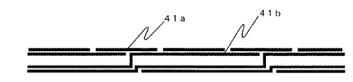
次に、請求項1に基ずく抵抗性周囲電極13について、説明する。図4a及びbに図1aの抵抗性周囲電極13の部分拡大図を示す。尚、図4bは階段状パターンの垂直部で結合した形状である。4角形の座標入力パネル11の面抵抗体12上に配置された4辺のうち、下辺の中央部分を示したものである。本実施の形態では、第一の直線状の導電性セグメント41aと第二の階段状の導電性セグメント41bの2種類の形状の導電性セグメントによって抵抗性周囲電極13が形成されている。また、図4cは、図4a及びbの応用例であり、第一の直線状の導電性セグメント41aと第二の階段状の導電性セグメント41bと最も外側に第三の破線状の導電性セグメント41cによって抵抗性周囲電極13が形成されている。
抵抗性周囲電極13の一辺において第一の直線状の導電性セグメント41aの間隔53は、離れすぎると抵抗性周囲電極近傍の座標位置検出に歪みが発生してしまうため間隔を詰めた方が良い。
よって間隔の距離は、入力する手段により変わるが、入力する部材の幅の半分以下の距離が適切である。例えば指による入力の場合、指の幅(約10mm)の半分である5mm以下が望ましい。また、第一の直線状の導電性セグメント41aの隣合う一片の長さは少なくとも交互に同じ長さになるようにし、隣合う一片が同じ長さであっても問題なく、第一の直線状の導電性セグメント41aの間隔を満たすように適宜選択すればよい。
第一の直線状の導電性セグメント41aは、第一の直線状の導電性セグメント41aと隣接する第二の階段状の導電性セグメント41bの最上段(抵抗性周囲電極13の座標入力領域18に最も近い側の段)の中央部に1片、また、最上段の両端部に1片の半分が懸るよう、且つ、平行に配置される。図4a及びbのの抵抗性周囲電極13の場合、第一の直線状の導電性セグメント41aと第二の階段状の導電性セグメント41bの間隔は、第二の階段状の導電性セグメント41b間との抵抗値の関係に応じて適宜設計する。また、図4cの抵抗性周囲電極13の場合も第一の直線状の導電性セグメント41aと第二の階段状の導電性セグメント41bの間隔、第二の階段状の導電性セグメント41b間との抵抗値、第三の直線状の導電性セグメント41cの長さと、第二の階段状の導電性セグメント41bと第三の直線状の導電性セグメント41cとの抵抗値の関係に応じて適宜設計する。
さらに、第二の階段状の導電性セグメント41bは、階段状の構成部材が、隣接し平行に重なり合うように配置され、且つ、平行に重なり合う段が少なくとも2段以上あるようにする。また、階段状の段形状において、段の角は、鋭角または鈍角であってもよいし、丸みを持たせてもよい。
抵抗性周囲電極13の辺の端部、つまり検出電極(図1aの14、15、16及び17)に最も近い導電性セグメント41bは、抵抗性周囲電極13の一辺において、電気的に直線的な抵抗値変化になるようにし配置させる。
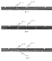
次に、請求項2に基ずく抵抗性周囲電極13について、説明する。図5a及びbに図1bの抵抗性周囲電極13の部分拡大図を示す。4角形の座標入力パネル11の面抵抗体12上に配置された4辺のうち、下辺の中央部分を示したものである。本実施の形態では、第一の直線状の導電性セグメント41aと第二の階段状の導電性セグメント41bの2種類の形状の導電性セグメントによって抵抗性周囲電極13が形成されている。また、図5cは、図5a及びbの応用例であり、第一の直線状の導電性セグメント41aと第二の階段状の導電性セグメント41bと最も外側に第三の破線状の導電性セグメント41cによって抵抗性周囲電極13が形成されている。
抵抗性周囲電極13の一辺において第一の直線状の導電性セグメント41aの間隔は、離れすぎると抵抗性周囲電極近傍の座標位置検出に歪みが発生してしまうため間隔を詰めた方が良い。
よって間隔の距離は、入力する手段により変わるが、入力する部材の幅の半分以下の距離が適切である。例えば指による入力の場合、指の幅(約10mm)の半分である5mm以下が望ましい。また、第一の直線状の導電性セグメント41aの隣合う一片の長さは同じ長さになるようにし、第一の直線状の導電性セグメント41aの間隔を満たすように適宜選択すればよい。第一の直線状の導電性セグメント41aは、第一の直線状の導電性セグメント41aと隣接する第二の階段状の導電性セグメント41bの最上段(抵抗性周囲電極13の座標入力領域18に最も近い側の段)の両端部に1片の半分が懸るよう、且つ、平行に配置される。図4a及びbのの抵抗性周囲電極13の場合、第一の直線状の導電性セグメント41aと第二の階段状の導電性セグメント41bの間隔は、第二の階段状の導電性セグメント41b間との抵抗値の関係に応じて適宜設計する。また、図4cの抵抗性周囲電極13の場合も第一の直線状の導電性セグメント41aと第二の階段状の導電性セグメント41bの間隔、第二の階段状の導電性セグメント41b間との抵抗値、第三の直線状の導電性セグメント41cの長さと、第二の階段状の導電性セグメント41bと第三の直線状の導電性セグメント41cとの抵抗値の関係に応じて適宜設計する。
さらに、第二の階段状の導電性セグメント41bは、階段状の構成部材が、隣接し平行に重なり合うように配置され、且つ、平行に重なり合う段が少なくとも2段以上あるようにする。また、階段状の段形状において、段の角は、鋭角または鈍角であってもよいし、丸みを持たせてもよい。
抵抗性周囲電極13の辺の端部、つまり検出電極(図1bの14、15、16及び17)に最も近い導電性セグメント41bは、抵抗性周囲電極13の一辺において、電気的に直線的な抵抗値変化になるようにし配置させる。
次に、請求項3に基づく抵抗性周囲電極13について、説明する。図7に図2aの抵抗性周囲電極13の部分拡大図を示したものである。4角形の座標入力パネル11の面抵抗体12上に配置された4辺のうち、下辺の左半分を、検出電極17と共に示したものである。本実施の形態では、1辺の半分が、第一の直線状の導電性セグメント41aと第二の階段状の導電性セグメント41bの2種類の形状の導電性セグメントによって形成されおり、図6に示した抵抗性周囲電極と配置、構成等が同じである。一方、辺の中央に最も近い導電性セグメント41bで、辺の中央に関して対称な配置を持つ、下辺の右半分の導電性セグメントのうち、辺の中央に最も近い導電性セグメントと接続させる。第二の階段状の導電性セグメントの段形状は、好ましくは、図7に示した下辺の左半分において、左下がりに、右半分においては、逆に右下がりの段形状にした方が良いが、下辺の左半分において、右下がりに、右半分においては、逆に左下がりの段形状にしても良い。導電性セグメントの配置パターンは、抵抗性周囲電極13の各辺の中央に関してそれぞれ対称であることが好ましい。しかし、配置パターンは各辺の間で同一である必要はない。線対称にすることにより検出電極近傍のパターンも対称にでき、抵抗性周囲電極の長さによる抵抗変化をより直線的にできる。また、階段状の段形状において、段の角は、鋭角または鈍角であってもよいし、丸みを持たせてもよい。
1辺を構成する導電性セグメントの数は、多ければ、座標入力領域18において、より抵抗性周囲電極13の間際まで、指示位置の座標の計算結果の歪みを小さくすることができる。しかし、導電性セグメントの数が多くなると、それらの間隙によって構成される抵抗値の合計が大きくなる傾向にある。
一方、導電性セグメントを長くすると対向した導電性セグメントとの重なる部分が大きくなり、抵抗性周囲電極13の抵抗値を下げることができる。しかし、導電性セグメントが長くなることで指が移動しても指からの分配される信号の変化が少なくなり、正確な位置が検出できなくなる。そこで、第一の直線状の導電性セグメント41aの長さを調整し、第二の階段状の導電性セグメント41bの座標入力領域側に形成し、第一の直線状の導電性セグメント41aの3片まで第二の階段状の導電性セグメント41bの片を長くすることにより、正確な位置が検出できるようになる。
以上のように、導電性セグメントの数、間隙、及び重なり合う長さなどを調整して、抵抗性周囲電極13の辺あたりの抵抗値、つまり隣り合う検出電極間の抵抗値を適切な範囲にする必要がある。
指21からのAC信号が面抵抗体12を通して流れ、抵抗性周囲電極13を介して検出電極14〜17へ配分される電流値を測定して指示位置の座標を計算するものであるが、抵抗性周囲電極13と指21の位置が近いと指21から直接、第二の階段状の導電性セグメントの2段目以下の段へAC信号が流れる現象が起きる。(信号の飛び込み)
この指21からの信号の飛び込みが存在すると、計算される座標が、指21から信号が飛び込んだ第二の階段状の導電性セグメントの最上段が位置する方向へずれる傾向がある。
上記問題を解決するには、図4、5のパターンを図8に示すように第一の直線状の導電性セグメント41aと隣接する第二の階段状の導電性セグメント41bの最上段と上から2段目の間隔を広げることで、指21から第二の階段状の導電性セグメント41bの2段目以下の段への飛び込みを抑制することができる。これを抑制することは、抵抗性周囲電極13の間際における座標の計算結果の正確性に寄与する。段の間隔を広げた場合、抵抗値を適切な値に調整するため、適宜、段数を増加させることも必要である。
図9に、図6、及び7に示した抵抗性周囲電極13の部分拡大図を説明するための概念図を示す。図9では、第一の直線状の導電性セグメント41aと第二の階段状の導電性セグメント41bを実際の前記両セグメントより極細な直線で示し、配置のパターンを明瞭にするために、間隙を広く示した。面抵抗体12(図示せず)のうち、図9(a)に43a〜43cで示し、平行に並んで隣り合う第二の階段状の導電性セグメント41bの間隙の部分43cが、抵抗性周囲電極13の辺あたりの抵抗値に最も寄与する。より厳密には、導電性セグメント自体の抵抗値があるが導電性セグメント間の抵抗値に比べて非常に小さく無視できる。
図9(a)に43a〜43cで示した、面抵抗体12の部分は、平行に並んで隣り合う導電性セグメント41aまたは41bのそれぞれの間隙の抵抗として、等価的に、図9(b)に示す抵抗42a〜42cとして表現することができる。つまり、階段状の重なり合う平行部の長さと段層の垂直になる平行部、及び、隣合う端部での電気的な広がりを考慮すると、抵抗性周囲電極13は、これらの等価的な抵抗42a〜42cが直並列に接続されたものと見做すことができる。そして、等価的な抵抗42a〜42cのそれぞれの抵抗値は、面抵抗体12の抵抗値、平行に並んで隣り合う導電性セグメント41aまたは41bのそれぞれの間隙の距離d、及び2段の重なり合う長さL1、L2と段層の垂直部の平行に重なり合う長さHの和wによって求めることができる。
面抵抗体12の抵抗値は、一般的に、シート抵抗で表される。面抵抗体12のシート抵抗をρ(Ω/□)とすると、抵抗42の抵抗値は、ρ×d/w(Ω)という式で計算することができる。また、導電性セグメントそれぞれの間隙とそれぞれの重なり合う長さを用いて抵抗計算すれば、抵抗性周囲電極13の1辺は直並列抵抗の回路となり、その合成抵抗は容易に計算できる。
次に抵抗性周囲電極の一辺における抵抗の直線性について説明する。
図10は座標入力パネル表面に形成している面抵抗体の電位分布の模式図であり、図1の4つの検出電極14,15,16,17のうち検出電極4に電圧を印加し、検出電極16をグランドとしたときの面抵抗体12に発生する電位分布を等電位線45で示したものである。
この際検出電極14−15間、15−16間、16−17間、17−14間の抵抗性周囲電極13の抵抗値の直線性が良好な場合、すなわち単位長さ当たりの抵抗値が一定の場合には、等電位線45が直線となる。逆に、抵抗性周囲電極13の抵抗値の直線性が悪い場合、例えば抵抗性周囲電極13の46近傍で抵抗値に異常があった場合には、図11のように等電位線45が歪むことになり、座標検出の精度が悪くなる。
本発明による抵抗性周囲電極13は第一の導電性セグメント41は破線状に配列されているため、前記抵抗値の直線性は、第一の導電性セグメント41aの中央部分間の距離を用いて単位長さ当たりの抵抗値が一定になるよう設計すればよい。
図12aは本発明による1実施例の抵抗性周囲電極13の一部の部分拡大図(抵抗成分を図47a〜47fで示す)であり、図12bは図12aの等価回路図である。
R1、R2は抵抗性周囲電極13の第一の導電性セグメント41aの長さによる抵抗値、R3は抵抗性周囲電極13の第二の導電性セグメント41bの長さによる抵抗値、R4、R4、R6は各パターンの間隙による抵抗値である。
図12bにおいて、R4、R5、R6はR1、R2、R3に対し、無視できるほど大きいと仮定すると、A間の等価回路は図13aのようになり、A間の抵抗値Raは2×R2×(R2+R3)/(2×R2+R3)となる。
また同様にB間の等価回路は図13bのようになり、B間の抵抗値はRbは2×R1+(2×R2×R3)/(2×R2+R3)となる。
A間及びB間の抵抗値が等しくなるように前記式をR1で解くと、R1=R2^2/(2×R2+R3)となる。
従って、本式を用いて、図12aの第一の導電性セグメント41aの破線の長さを、抵抗値がR1、R2になるように交互に同じ長さにすることにより、抵抗性周囲電極13の抵抗値の直線性を良くすることができる。実際には、R4,R5、R6による誤差が多少あるので、必要に応じて適宜調整すればよい。
また検出電極14〜17の近傍では、R3、R4、R5が他の部分と異なる値になるので、抵抗性周囲電極13の抵抗値の直線性が良くなるように検出部14〜17と接触しているパターンの長さを適宜調整すればよい。
さらに検出電極14〜17の近傍で、抵抗性周囲電極13の抵抗値の直線性良く、且つ効率的にパターン設計を行うためには、図2a及び図2bのように抵抗性周囲電極13を各抵抗性周囲電極13の中央部で線対称になるよう配置することが、好ましい。
次に請求項4に基ずく抵抗性周囲電極13について説明する。図14a〜cに、図1aまたは図2aの抵抗性周囲電極13の部分拡大図を示したものである。4角形の座標入力パネル11の面抵抗体12上に配置された4辺のうち、下辺の左半分を、検出電極17と共に示したものである。本実施の形態では、検出電極17近傍を抵抗性周囲電極13の端部とした場合、第一の直線状の導電性セグメント41aは、検出電極17と面抵抗体12を介して間接的に接触している。一方、第二の階段状の導電性セグメント41bは、第一の直線状の導電性セグメント41aに近い段では、検出電極17に直接接続している。また、第一の直線状の導電性セグメント41aに近い段以外の第二の階段状の導電性セグメント41bの段と検出電極17は、抵抗性周囲電極13の一辺において、電気的に直線的な抵抗値変化になるように、直接接触させるか面抵抗体12を介して間接的に接触させるかを適宜選択し配置する。
次に請求項5に基ずく抵抗性周囲電極13について説明する。図3に示すように指21からのAC信号が面抵抗体12を通して流れ、抵抗性周囲電極13を介して検出電極14〜17へ配分される電流値を測定して指示位置の座標を計算するものであるが、抵抗性周囲電極13と指21の位置が近いと指21から直接、第二の階段状の導電性セグメントの2段目以下の段へAC信号が流れる現象が起きる。(信号の飛び込み)
この指21からの信号の飛び込みが存在すると、計算される座標が、指21から信号が飛び込んだ第二の階段状の導電性セグメントの最上段が位置する方向へずれる傾向がある。
上記問題を解決するには、図4、5のパターンを図8(図4aのみを示す)に示すように第一の直線状の導電性セグメント41aと隣接する第二の階段状の導電性セグメント41bの最上段と上から2段目の間隔を広げることで、指21から第二の階段状の導電性セグメント41bの2段目以下の段への飛び込みを抑制することができる。これを抑制することは、抵抗性周囲電極13の間際における座標の計算結果の正確性に寄与する。段の間隔を広げた場合、抵抗値を適切な値に調整するため、適宜、段数を増加させることも必要である。
Next, the
If the
Therefore, although the distance of an interval changes with the means to input, the distance of less than half of the width of the member to input is suitable. For example, in the case of input by a finger, 5 mm or less, which is a half of the finger width (about 10 mm), is desirable. Further, the lengths of adjacent pieces of the first linear conductive segments 41a are at least alternately the same length, and there is no problem even if the adjacent pieces have the same length. What is necessary is just to select suitably so that the space | interval of this conductive segment 41a may be satisfy | filled.
The first linear conductive segment 41a is the uppermost step of the second step-shaped
Further, the second step-like
The
Next, the
If the distance between the first linear conductive segments 41a on one side of the resistive surrounding
Therefore, although the distance of an interval changes with the means to input, the distance of less than half of the width of the member to input is suitable. For example, in the case of input by a finger, 5 mm or less, which is a half of the finger width (about 10 mm), is desirable. Moreover, the length of the adjacent piece of the first linear conductive segment 41a may be the same length, and may be appropriately selected so as to satisfy the interval between the first linear conductive segments 41a. The first linear conductive segment 41a is the uppermost step of the second step-shaped
Further, the second step-like
The
Next, the
If the number of the conductive segments constituting one side is large, it is possible to reduce the distortion of the calculation result of the coordinates of the indicated position in the coordinate
On the other hand, when the conductive segment is lengthened, the overlapping portion with the opposing conductive segment becomes large, and the resistance value of the resistive surrounding
As described above, by adjusting the number of conductive segments, the gap, the overlapping length, and the like, the resistance value per side of the resistive surrounding
The AC signal from the
When the signal jump from the
In order to solve the above problem, as shown in FIG. 8, the pattern of FIGS. 4 and 5 is formed from the uppermost step of the second step-like
FIG. 9 is a conceptual diagram for explaining a partially enlarged view of the resistive surrounding
The portion of the
The resistance value of the
Next, the linearity of resistance on one side of the resistive surrounding electrode will be described.
FIG. 10 is a schematic diagram of the potential distribution of the surface resistor formed on the surface of the coordinate input panel. A voltage is applied to the
At this time, when the linearity of the resistance value of the resistive surrounding
In the resistive surrounding
12a is a partial enlarged view of a part of the resistive surrounding
R1 and R2 are resistance values due to the length of the first conductive segment 41a of the resistive surrounding
In FIG. 12b, assuming that R4, R5, and R6 are negligibly larger than R1, R2, and R3, the equivalent circuit between A is as shown in FIG. 13a, and the resistance value Ra between A is 2 × R2 ×. (R2 + R3) / (2 × R2 + R3).
Similarly, the equivalent circuit between B is as shown in FIG. 13B, and the resistance value between B is R × 2 × R1 + (2 × R2 × R3) / (2 × R2 + R3).
When the above equation is solved by R1 so that the resistance values between A and B are equal, R1 = R2 ^ 2 / (2 × R2 + R3).
Therefore, by using this equation, the length of the broken line of the first conductive segment 41a in FIG. 12a is alternately made the same length so that the resistance values become R1 and R2, thereby the resistive surrounding
Further, in the vicinity of the
Further, in order to efficiently perform pattern design in the vicinity of the
Next, the
Next, the
When the signal jump from the
To solve the above problem, the second stepped conductive segment adjacent to the first linear conductive segment 41a as shown in FIG. 8 (only FIG. 4a is shown) in the pattern of FIGS. By expanding the distance between the uppermost step of 41b and the second step from the top, it is possible to prevent the
以上のように抵抗性周囲電極の抵抗値は、面抵抗体12の抵抗値と導電性セグメントのパターンより決定される。よって、従来ではパネル毎に面抵抗体の抵抗値が違っていた場合にはそれにあわせて抵抗性周囲電極の抵抗値を適切な値に変更・調整する必要があるが、本発明による抵抗性周囲電極は、面抵抗体12の抵抗値変化によって抵抗性周囲電極の抵抗値が変化することにより、パネル毎による面抵抗のばらつきによる抵抗性周囲電極の抵抗調整が必要なくなる。
As described above, the resistance value of the resistive surrounding electrode is determined by the resistance value of the
以下、実施例及び比較例により、本発明を説明する。本発明は、以下の実施例に限定されるものでなく、本発明の技術範囲において、種々の変形例を含むものである。
(実施例1)
実施例1
座標入力パネル11は、次のようにして作成した。ガラス基材として、ソーダガラス(厚さ3ミリ)を略469×375mmの大きさに切断したものを用い、ガラス基材の表面に、スパッタ法によってITO(錫を添加した酸化インジウム)膜(シート抵抗値300Ω/□)を形成して面抵抗体12とした。次に、抵抗性周囲電極13の導電性セグメント、及び検出電極14〜17を、(株)アサヒ化学研究所製銀ペーストLS−504(樹脂バインダー)をスクリーン印刷し、加熱硬化させることで形成した。
抵抗性周囲電極13のパターンは図4aのパターンを用い、一片を図2aの様な線対称の形状にし、四隅は図14aに示したように少なくとの第二の階段状の導電性セグメント41bが、第一の直線状の導電性セグメント41aに近い段で、検出電極17に直接接続させた。また、導電性セグメントは、表1の寸法条件(図16a参照)で座標入力パネル11を作成した。
Hereinafter, the present invention will be described with reference to examples and comparative examples. The present invention is not limited to the following examples, and includes various modifications within the technical scope of the present invention.
Example 1
Example 1
The coordinate input panel 11 was created as follows. A glass substrate made of soda glass (
The pattern of the resistive surrounding

実施例1において、導電性セグメントを、表1の寸法条件(図16a参照)のパターンを用いた以外は、実施例1と同作成条件で座標入力パネル11を作成した。
(実施例3)
抵抗性周囲電極13のパターン図4bのパターンを用い、一片を図1aの様な同じ形状が連なるようにし、四隅は図14bに示したように少なくとの第二の階段状の導電性セグメント41bが、第一の直線状の導電性セグメント41aに近い段で、検出電極17に直接接続させた。また、導電性セグメントが、表1の寸法条件(図16b参照)のパターンを用いた以外は、実施例1と同作成条件で座標入力パネル11を作成した。
(実施例4)
実施例3の図1aにおいて、対辺を対称にし、導電性セグメントが表1の寸法条件(図16b参照)のパターンを用いた以外は、実施例1と同作成条件で座標入力パネル11を作成した。
(実施例5)
抵抗性周囲電極13のパターン図4cのパターンを用い、一片を図2aの様な線対称の形状にし、四隅は図14cに示したように少なくとの第二の階段状の導電性セグメント41bが、第一の直線状の導電性セグメント41aに近い段で、検出電極17に直接接続させた。また、導電性セグメントが、表1の寸法条件(図16c参照)のパターンを用いた以外は、実施例1と同作成条件で座標入力パネル11を作成した。
(実施例6)
実施例5において、導電性セグメントが、表1の寸法条件(図16c参照)のパターンを用いた以外は、実施例1と同作成条件で座標入力パネル11を作成した。
(実施例7)
抵抗性周囲電極13のパターン図5aのパターンを用い、一片を図2bの様な線対称の形状にし、四隅は図14aに示したように少なくとの第二の階段状の導電性セグメント41bが、第一の直線状の導電性セグメント41aに近い段で、検出電極17に直接接続させた。また、導電性セグメントが、表1の寸法条件(図17a参照)のパターンを用いた以外は、実施例1と同作成条件で座標入力パネル11を作成した。
(実施例8)
抵抗性周囲電極13のパターン図5bのパターンを用い、一片を図1bの様な同じ形状が連なるようにし、対辺が対称にし、四隅は図14bに示したように少なくとの第二の階段状の導電性セグメント41bが、第一の直線状の導電性セグメント41aに近い段で、検出電極17に直接接続させた。また、導電性セグメントが、表1の寸法条件(図17b参照)のパターンを用いた以外は、実施例1と同作成条件で座標入力パネル11を作成した。
(実施例9)
抵抗性周囲電極13のパターン図5cのパターンを用い、一片を図2bの様な線対称の形状にし、四隅は図14cに示したように少なくとの第二の階段状の導電性セグメント41bが、第一の直線状の導電性セグメント41aに近い段で、検出電極17に直接接続させた。また、導電性セグメントが、表1の寸法条件(図17c参照)のパターンを用いた以外は、実施例1と同作成条件で座標入力パネル11を作成した。
(実施例10)
実施例1において、図8のように第一の直線状の導電性セグメント41aに最も近い第二の階段状セグメントの段を変更したパターンにした。また、導電性セグメントが、表1の寸法条件(図16a参照)のパターンを用いた以外は、実施例1と同作成条件で座標入力パネル11を作成した。
(実施例11)
実施例4において、図8のように第一の直線状の導電性セグメント41aに最も近い第二の階段状セグメントの段を変更したパターンにした。また、導電性セグメントは、導電性セグメントが、表1の寸法条件(図16b参照)のパターンを用いた以外は、実施例1と同作成条件で座標入力パネル11を作成した。
(実施例12)
実施例5において、図8のように第一の直線状の導電性セグメント41aに最も近い第二の階段状セグメントの段を変更したパターンにした。また、導電性セグメントは、導電性セグメントが、表1の寸法条件(図16c参照)のパターンを用いた以外は、実施例1と同作成条件で座標入力パネル11を作成した。
(実施例13、14、及び、15)
実施例1において、破線長さA(51)、破線長さB(52)、破線間隔(53)を変更したパターンにした。また、導電性セグメントが、表1の寸法条件(図16a参照)のパターンを用いた以外は、実施例1と同作成条件で座標入力パネル11を作成した。
(実施例16、17、及び、18)
面抵抗体12のシート抵抗値を500、700、及び、900Ω/□にした以外は実施例1と同条件にて座標入力パネル11を作成した。
(実施例19、20、及び、21)
面抵抗体12のシート抵抗値を500、700、及び、900Ω/□にした以外は実施例2と同条件にて座標入力パネル11を作成した。
(実施例22、23、及び、24)
面抵抗体12のシート抵抗値を500、700、及び、900Ω/□にした以外は実施例3と同条件にて座標入力パネル11を作成した。
(実施例25、26、及び27)
面抵抗体12のシート抵抗値を500、700、及び、900Ω/□にした以外は実施例4と同条件にて座標入力パネル11を作成した。
(実施例28、29、及び30)
面抵抗体12のシート抵抗値を500、700、及び、900Ω/□にした以外は実施例5と同条件にて座標入力パネル11を作成した。
(実施例31、32及び33)
面抵抗体12のシート抵抗値を500、700、及び、900Ω/□にした以外は実施例6と同条件にて座標入力パネル11を作成した。
(実施例34、35、及び、36)
面抵抗体12のシート抵抗値を500、700、及び、900Ω/□にした以外は実施例7と同条件にて座標入力パネル11を作成した。
(実施例37、38、及び39)
面抵抗体12のシート抵抗値を500、700、及び、900Ω/□にした以外は実施例8と同条件にて座標入力パネル11を作成した。
(実施例40、41、及び、42)
面抵抗体12のシート抵抗値を500、700、及び、900Ω/□にした以外は実施例9と同条件にて座標入力パネル11を作成した。
(比較例1)
座標入力パネル11(図15)は、次のようにして作成した。ガラス基材として、ソーダガラス(厚さ3ミリ)を略469×375mmの大きさに切断したものを用い、ガラス基材の表面に、スパッタ法によってITO(錫を添加した酸化インジウム)膜を形成して面抵抗体12とした。
次に、抵抗性周囲電極13、面抵抗体12の上に(株)アサヒ化学研究所製銀ペーストls−504(樹脂バインダー)にカーボンを混合したペーストを用いて、スクリー ン印刷により印刷し、180℃にて30分加熱硬化した。その際、抵抗性周囲電極2の4頂点間抵抗値が約100Ωになるように、パターン 幅・長さが設計されたパターンを用いた。
また、検出電極14〜17を、(株)アサヒ化学研究所製銀ペーストLS−504(樹脂バインダー)をスクリーン印刷し、加熱硬化させることで形成した。このとき、座標入力領域18の大きさを略450×350mmとした。
更に、面抵抗体12上に、透明絶縁性基材を形成した。透明絶縁性基材を形成するには、面抵抗体12と抵抗性周囲電極13上にガラスペーストを印刷し、熱処理して粉末ガラスを溶融させ、焼結させた。最後に、検出電極14〜17上に、引き出し線22〜25を、ハンダ付けにより接続した。この際、面抵抗体12のシート抵抗は300Ω/□となるようにした。
(比較例2、3、及び、4)
面抵抗体12のシート抵抗は500、700、及び、900Ω/□にした以外は、比較例1と同条件で座標入力パネル11を作成した。
(比較例5)
41aの長さ1mm、41a同士の間隔を8.5mmにした以外は、実施例13と同条件でパターンを作成し座標入力パネル11を作成した。
作成した座標入力パネル11を、図3に示した構成図のように作成したハードウエアに接続した。ただし、CPU31から出力される座標データを、シリアル通信によってパソコンに取り込むようにした。
この座標入力システムを用いて座標入力パネル11を評価した(表2)。その結果、実施例1〜42において抵抗性周囲電極一辺における抵抗値の直線性は良く、特に実施例5、6、9、12、20、21、24、29、30、33、38、39、42が良かった。トレース結果においても本実施例1〜42において座標入力領域において全体のトレース線の歪みがなかった。さらに、抵抗性周囲電極近傍の微小な歪みも実施例1〜42は極微小であったが、なかでも実施例15はより極微小なであった。
また、面抵抗体の抵抗値が異なるものに本パターンを作成した実施例16〜42においても他の実施例と同様な抵抗値の直線性とトレース線の歪みがないことが確認できたことから、面抵抗体の抵抗値に依存しない抵抗性周囲電極パターンを得ることができた。
一方、比較例1〜4においては直線型帯形状であるため抵抗値の直線性は得られるが、面抵抗値が異なるとトレース線に歪みが発生してしまった。また、比較例5は第一の直線状の導電性セグメントの破線は短いためトレース線に歪みが生じてしまった。
In Example 1, the coordinate input panel 11 was created under the same creation conditions as in Example 1 except that the conductive segment used the pattern of the dimensional conditions in Table 1 (see FIG. 16a).
(Example 3)
Pattern of
Example 4
In FIG. 1a of Example 3, the coordinate input panel 11 was created under the same creation conditions as in Example 1 except that the opposite sides were symmetrical and the conductive segments used the pattern of the dimension conditions in Table 1 (see FIG. 16b). .
(Example 5)
Pattern of
(Example 6)
In Example 5, the coordinate input panel 11 was created under the same creation conditions as in Example 1 except that the conductive segment used the pattern of the dimensional conditions in Table 1 (see FIG. 16c).
(Example 7)
Pattern of resistive surrounding
(Example 8)
Pattern of resistive surrounding
Example 9
The pattern of the resistive surrounding
(Example 10)
In Example 1, the pattern of the second stepped segment closest to the first linear conductive segment 41a was changed as shown in FIG. Moreover, the coordinate input panel 11 was created on the same creation conditions as Example 1 except the conductive segment using the pattern of the dimension conditions of Table 1 (refer FIG. 16a).
(Example 11)
In Example 4, as shown in FIG. 8, the pattern of the second stepped segment closest to the first linear conductive segment 41a was changed. Moreover, the conductive segment produced the coordinate input panel 11 on the same creation conditions as Example 1 except that the conductive segment used the pattern of the dimensional conditions of Table 1 (refer FIG. 16b).
(Example 12)
In Example 5, the pattern of the second stepped segment closest to the first linear conductive segment 41a was changed as shown in FIG. Moreover, the conductive segment produced the coordinate input panel 11 on the same creation conditions as Example 1 except that the conductive segment used the pattern of the dimension conditions of Table 1 (refer FIG. 16c).
(Examples 13, 14, and 15)
In Example 1, it was set as the pattern which changed broken line length A (51), broken line length B (52), and broken line space | interval (53). Moreover, the coordinate input panel 11 was created on the same creation conditions as Example 1 except the conductive segment using the pattern of the dimension conditions of Table 1 (refer FIG. 16a).
(Examples 16, 17, and 18)
The coordinate input panel 11 was created under the same conditions as in Example 1 except that the sheet resistance value of the
(Examples 19, 20, and 21)
The coordinate input panel 11 was created under the same conditions as in Example 2 except that the sheet resistance value of the
(Examples 22, 23, and 24)
A coordinate input panel 11 was created under the same conditions as in Example 3 except that the sheet resistance value of the
(Examples 25, 26, and 27)
The coordinate input panel 11 was created under the same conditions as in Example 4 except that the sheet resistance value of the
(Examples 28, 29, and 30)
A coordinate input panel 11 was created under the same conditions as in Example 5 except that the sheet resistance value of the
(Examples 31, 32 and 33)
A coordinate input panel 11 was created under the same conditions as in Example 6 except that the sheet resistance value of the
(Examples 34, 35, and 36)
A coordinate input panel 11 was created under the same conditions as in Example 7 except that the sheet resistance value of the
(Examples 37, 38, and 39)
A coordinate input panel 11 was created under the same conditions as in Example 8 except that the sheet resistance value of the
(Examples 40, 41, and 42)
A coordinate input panel 11 was created under the same conditions as in Example 9 except that the sheet resistance value of the
(Comparative Example 1)
The coordinate input panel 11 (FIG. 15) was created as follows. As a glass substrate, soda glass (
Next, printing is performed on the resistive surrounding
Moreover, the detection electrodes 14-17 were formed by screen-printing and heat-curing silver paste LS-504 (resin binder) made by Asahi Chemical Laboratory. At this time, the size of the coordinate
Further, a transparent insulating base material was formed on the
(Comparative Examples 2, 3, and 4)
A coordinate input panel 11 was prepared under the same conditions as in Comparative Example 1 except that the sheet resistance of the
(Comparative Example 5)
A coordinate input panel 11 was created by creating a pattern under the same conditions as in Example 13 except that the length of 41a was 1 mm and the interval between 41a was 8.5 mm.
The created coordinate input panel 11 was connected to the created hardware as shown in the block diagram of FIG. However, coordinate data output from the CPU 31 is taken into a personal computer by serial communication.
The coordinate input panel 11 was evaluated using this coordinate input system (Table 2). As a result, the linearity of the resistance value on one side of the resistive surrounding electrode in Examples 1-42 is good, and in particular, Examples 5, 6, 9, 12, 20, 21, 24, 29, 30, 33, 38, 39, 42 was good. Also in the trace results, in Examples 1-42, there was no distortion of the entire trace line in the coordinate input area. Furthermore, the minute distortion in the vicinity of the resistive surrounding electrode was extremely small in Examples 1 to 42, and in particular, Example 15 was extremely small.
Also, in Examples 16 to 42 in which this pattern was created with different resistance values of the surface resistor, it was confirmed that there was no resistance linearity and trace line distortion similar to other examples. Thus, it was possible to obtain a resistive surrounding electrode pattern independent of the resistance value of the surface resistor.
On the other hand, in Comparative Examples 1 to 4, since the linear belt shape is used, the resistance value linearity can be obtained. However, if the surface resistance values are different, the trace lines are distorted. Further, in Comparative Example 5, since the broken line of the first linear conductive segment is short, the trace line is distorted.
1 座標入力パネル
2 面抵抗体
3 抵抗性周囲電極
4、5、6、7 検出電極
8 座標入力領域
11 座標入力パネル
12 面抵抗体
13 抵抗性周囲電極
14、15、16、17 検出電極
18 座標入力領域
21 指
22、23、24、25 引き出し線
26 アナログ信号処理部
27 振動電圧印加回路
28 振動電圧発生器
29 アナログマルチプレクサ
30 A/Dコンバータ
31 CPU
41a、41b 、41c 導電性セグメント
42a、42b、42c 等価的な抵抗
43a、43b、43c 平行に並んで隣り合う導電性セグメントの間隙
45 等電位線
46 抵抗性周囲電極13の抵抗値異常部位
47a、47b、47c、47d、47e、47f 等価的な抵抗
50 第一の直線状の導電性セグメントにおける破線線幅
51 第一の直線状の導電性セグメントにおける破線線長さA
52 第一の直線状の導電性セグメントにおける破線線長さB
53 第一の直線状の導電性セグメントにおける破線間隔
54 第二の階段状の導電性セグメントにおける階段線幅
55 第二の階段状の導電性セグメントにおける階段間隙
56 第二の階段状の導電性セグメントにおける階段の重なり長さ
57 第二の階段状の導電性セグメントにおける階段一段部の間隙
DESCRIPTION OF
41a, 41b,
52 Broken line length B in first linear conductive segment
53 Distance between
Claims (5)
Priority Applications (1)
| Application Number | Priority Date | Filing Date | Title |
|---|---|---|---|
| JP2011239019A JP5970776B2 (en) | 2010-11-01 | 2011-10-31 | Coordinate input panel |
Applications Claiming Priority (5)
| Application Number | Priority Date | Filing Date | Title |
|---|---|---|---|
| JP2010245495 | 2010-11-01 | ||
| JP2010245495 | 2010-11-01 | ||
| JP2011041049 | 2011-02-28 | ||
| JP2011041049 | 2011-02-28 | ||
| JP2011239019A JP5970776B2 (en) | 2010-11-01 | 2011-10-31 | Coordinate input panel |
Publications (2)
| Publication Number | Publication Date |
|---|---|
| JP2012194962A true JP2012194962A (en) | 2012-10-11 |
| JP5970776B2 JP5970776B2 (en) | 2016-08-17 |
Family
ID=47086750
Family Applications (1)
| Application Number | Title | Priority Date | Filing Date |
|---|---|---|---|
| JP2011239019A Active JP5970776B2 (en) | 2010-11-01 | 2011-10-31 | Coordinate input panel |
Country Status (1)
| Country | Link |
|---|---|
| JP (1) | JP5970776B2 (en) |
Citations (9)
| Publication number | Priority date | Publication date | Assignee | Title |
|---|---|---|---|---|
| JPS56500230A (en) * | 1979-02-23 | 1981-02-26 | ||
| JP2000081610A (en) * | 1998-08-18 | 2000-03-21 | Internatl Business Mach Corp <Ibm> | Liquid crystal display device |
| US20030137498A1 (en) * | 1998-10-09 | 2003-07-24 | 3M Innovative Properties Company | Touch panel with improved linear response and minimal border width electrode pattern |
| JP2004513440A (en) * | 2000-11-03 | 2004-04-30 | エロ・タッチシステムズ・インコーポレイテッド | Touch screen with multiple parallel connections to each electrode in the series resistor chain around the touch area |
| JP2005523531A (en) * | 2002-04-16 | 2005-08-04 | エロ・タッチシステムズ・インコーポレイテッド | Touch sensor with improved electrode pattern |
| JP2005530274A (en) * | 2002-06-14 | 2005-10-06 | スリーエム イノベイティブ プロパティズ カンパニー | Linearized conductive surface |
| JP2007517309A (en) * | 2003-12-30 | 2007-06-28 | スリーエム イノベイティブ プロパティズ カンパニー | Touch sensor with linear response |
| JP2009003913A (en) * | 2007-05-24 | 2009-01-08 | Gunze Ltd | Touch panel |
| JP2009252119A (en) * | 2008-04-09 | 2009-10-29 | Nec Lcd Technologies Ltd | Display device, liquid crystal display device, electronic equipment, and method for manufacturing display device |
-
2011
- 2011-10-31 JP JP2011239019A patent/JP5970776B2/en active Active
Patent Citations (9)
| Publication number | Priority date | Publication date | Assignee | Title |
|---|---|---|---|---|
| JPS56500230A (en) * | 1979-02-23 | 1981-02-26 | ||
| JP2000081610A (en) * | 1998-08-18 | 2000-03-21 | Internatl Business Mach Corp <Ibm> | Liquid crystal display device |
| US20030137498A1 (en) * | 1998-10-09 | 2003-07-24 | 3M Innovative Properties Company | Touch panel with improved linear response and minimal border width electrode pattern |
| JP2004513440A (en) * | 2000-11-03 | 2004-04-30 | エロ・タッチシステムズ・インコーポレイテッド | Touch screen with multiple parallel connections to each electrode in the series resistor chain around the touch area |
| JP2005523531A (en) * | 2002-04-16 | 2005-08-04 | エロ・タッチシステムズ・インコーポレイテッド | Touch sensor with improved electrode pattern |
| JP2005530274A (en) * | 2002-06-14 | 2005-10-06 | スリーエム イノベイティブ プロパティズ カンパニー | Linearized conductive surface |
| JP2007517309A (en) * | 2003-12-30 | 2007-06-28 | スリーエム イノベイティブ プロパティズ カンパニー | Touch sensor with linear response |
| JP2009003913A (en) * | 2007-05-24 | 2009-01-08 | Gunze Ltd | Touch panel |
| JP2009252119A (en) * | 2008-04-09 | 2009-10-29 | Nec Lcd Technologies Ltd | Display device, liquid crystal display device, electronic equipment, and method for manufacturing display device |
Also Published As
| Publication number | Publication date |
|---|---|
| JP5970776B2 (en) | 2016-08-17 |
Similar Documents
| Publication | Publication Date | Title |
|---|---|---|
| KR920003177B1 (en) | An electro satatic pattern-coupled digitizer | |
| JP5174575B2 (en) | Touch panel | |
| JP4718920B2 (en) | Coordinate detection device | |
| KR100698898B1 (en) | Touch Panel | |
| CN102645995B (en) | Touch screen and the display device of band touch screen and manufacture method thereof | |
| JP2012204127A (en) | Pressure sensitive switch | |
| US20170277308A1 (en) | Capacitive touch screen and method of manufacturing the same and touch control device | |
| US10061446B2 (en) | Touch panel using touch pen and formed with power pattern | |
| JP2005018138A (en) | Input device | |
| JP2013225266A (en) | Touch panel | |
| KR20150103612A (en) | Digitizer | |
| JP5831101B2 (en) | Coordinate input system | |
| JP5757800B2 (en) | Touch panel | |
| JP5970776B2 (en) | Coordinate input panel | |
| US8742882B2 (en) | Touch panel | |
| JP5768386B2 (en) | Coordinate input system | |
| JP3464306B2 (en) | Input tablet | |
| KR20090040695A (en) | Touch screen | |
| JP2007102377A (en) | Coordinate input panel | |
| JP2002041244A (en) | Resistor film type transparent analog touch panel | |
| JP2012190218A (en) | Capacitance type input device | |
| JP2011113481A (en) | Coordinate input panel | |
| JP5974540B2 (en) | Coordinate input system | |
| US6917358B2 (en) | Resistance inducting wire layout on a touch panel | |
| JP2016033698A (en) | Coordinate input system |
Legal Events
| Date | Code | Title | Description |
|---|---|---|---|
| A621 | Written request for application examination |
Free format text: JAPANESE INTERMEDIATE CODE: A621 Effective date: 20140827 |
|
| A977 | Report on retrieval |
Free format text: JAPANESE INTERMEDIATE CODE: A971007 Effective date: 20150629 |
|
| A131 | Notification of reasons for refusal |
Free format text: JAPANESE INTERMEDIATE CODE: A131 Effective date: 20150728 |
|
| A521 | Written amendment |
Free format text: JAPANESE INTERMEDIATE CODE: A523 Effective date: 20150821 |
|
| A131 | Notification of reasons for refusal |
Free format text: JAPANESE INTERMEDIATE CODE: A131 Effective date: 20160202 |
|
| A521 | Written amendment |
Free format text: JAPANESE INTERMEDIATE CODE: A523 Effective date: 20160208 |
|
| TRDD | Decision of grant or rejection written | ||
| A01 | Written decision to grant a patent or to grant a registration (utility model) |
Free format text: JAPANESE INTERMEDIATE CODE: A01 Effective date: 20160614 |
|
| A61 | First payment of annual fees (during grant procedure) |
Free format text: JAPANESE INTERMEDIATE CODE: A61 Effective date: 20160627 |
|
| R150 | Certificate of patent or registration of utility model |
Ref document number: 5970776 Country of ref document: JP Free format text: JAPANESE INTERMEDIATE CODE: R150 |