JP2012191069A - Solar cell module, manufacturing method therefor - Google Patents
Solar cell module, manufacturing method therefor Download PDFInfo
- Publication number
- JP2012191069A JP2012191069A JP2011054676A JP2011054676A JP2012191069A JP 2012191069 A JP2012191069 A JP 2012191069A JP 2011054676 A JP2011054676 A JP 2011054676A JP 2011054676 A JP2011054676 A JP 2011054676A JP 2012191069 A JP2012191069 A JP 2012191069A
- Authority
- JP
- Japan
- Prior art keywords
- layer
- electrode layer
- solar cell
- cell module
- compound semiconductor
- Prior art date
- Legal status (The legal status is an assumption and is not a legal conclusion. Google has not performed a legal analysis and makes no representation as to the accuracy of the status listed.)
- Withdrawn
Links
Images

Classifications
-
- Y—GENERAL TAGGING OF NEW TECHNOLOGICAL DEVELOPMENTS; GENERAL TAGGING OF CROSS-SECTIONAL TECHNOLOGIES SPANNING OVER SEVERAL SECTIONS OF THE IPC; TECHNICAL SUBJECTS COVERED BY FORMER USPC CROSS-REFERENCE ART COLLECTIONS [XRACs] AND DIGESTS
- Y02—TECHNOLOGIES OR APPLICATIONS FOR MITIGATION OR ADAPTATION AGAINST CLIMATE CHANGE
- Y02E—REDUCTION OF GREENHOUSE GAS [GHG] EMISSIONS, RELATED TO ENERGY GENERATION, TRANSMISSION OR DISTRIBUTION
- Y02E10/00—Energy generation through renewable energy sources
- Y02E10/50—Photovoltaic [PV] energy
- Y02E10/541—CuInSe2 material PV cells
-
- Y—GENERAL TAGGING OF NEW TECHNOLOGICAL DEVELOPMENTS; GENERAL TAGGING OF CROSS-SECTIONAL TECHNOLOGIES SPANNING OVER SEVERAL SECTIONS OF THE IPC; TECHNICAL SUBJECTS COVERED BY FORMER USPC CROSS-REFERENCE ART COLLECTIONS [XRACs] AND DIGESTS
- Y02—TECHNOLOGIES OR APPLICATIONS FOR MITIGATION OR ADAPTATION AGAINST CLIMATE CHANGE
- Y02P—CLIMATE CHANGE MITIGATION TECHNOLOGIES IN THE PRODUCTION OR PROCESSING OF GOODS
- Y02P70/00—Climate change mitigation technologies in the production process for final industrial or consumer products
- Y02P70/50—Manufacturing or production processes characterised by the final manufactured product
Landscapes
- Photovoltaic Devices (AREA)
Abstract
Description
本発明は、太陽電池モジュール、太陽電池モジュールの製造方法に関する。 The present invention relates to a solar cell module and a method for manufacturing a solar cell module.
従来、薄膜太陽電池の構造として、金属基板上に順番に裏面電極層/発電層/表面透明電極層を成膜したサブストレート構造が知られている。このサブストレート構造は、表面に形成した透明電極層側から光を入射させている。一方、透光性基板を光入射側とした構造(スーパーストレート構造)の薄膜太陽電池が報告されている。例えば、特許文献1に、透光性プラスチック基板上に、透明導電膜、光電変換層および裏面電極層が順次積層されてなる薄膜太陽電池が記載されている。スーパーストレート構造は、サブストレート構造と比較して部品数が低減するため、軽量化、コスト低減に効果がある。
Conventionally, as a structure of a thin film solar cell, a substrate structure in which a back electrode layer / a power generation layer / a surface transparent electrode layer are sequentially formed on a metal substrate is known. In this substrate structure, light is incident from the transparent electrode layer formed on the surface. On the other hand, a thin film solar cell having a structure (super straight structure) in which a light-transmitting substrate is a light incident side has been reported. For example,
太陽電池モジュールは、基本単位ユニットである太陽電池セルを複数個直列に接続することにより、所定の電圧を得ている。例えば、図5は、従来のスーパーストレート構造の薄膜太陽電池の製造工程を説明する図である。初めに、真空条件で透光性基板10上に成膜した透明電極層1をレーザスクライブ工程(LS)により短冊状(透明電極層1a,1b)に形成する(図5(a))。次に、スパッタリング法等によりバッファー層2および発電層3を形成し(図5(b))、続いて、メカニカルスクライブ工程(MS)により発電層3の一部をストライプ状に除去し(図5(c))、その後、裏面電極層4を形成し(図5(d))、最後に、裏面電極層4をメカニカルスクライブ工程(MS)により短冊状に分割する(図5(e))。
The solar cell module obtains a predetermined voltage by connecting a plurality of solar cells as basic unit units in series. For example, FIG. 5 is a diagram for explaining a manufacturing process of a conventional thin film solar cell having a super straight structure. First, the
このように、従来のスーパーストレート構造の薄膜太陽電池の製造工程においても、集積型構造の形成には、長時間を要するメカニカルスクライブ工程(MS)が複数回必要である。さらに、裏面電極層4は真空成膜工程により形成されるため、製造コストを増大させる。
本発明の目的は、スーパーストレート構造を有する薄膜太陽電池の製造方法をさらに改善することにある。
Thus, also in the manufacturing process of the conventional super straight structure thin film solar cell, the formation of the integrated structure requires a plurality of mechanical scribing steps (MS) that require a long time. Further, since the
An object of the present invention is to further improve the method for producing a thin film solar cell having a superstrate structure.
本発明によれば、下記(1)乃至(18)に係る発明が提供される。
(1)透光性基板上に順に成膜された第1電極層、吸収層及び第2電極層を備えた太陽電池モジュールであって、前記第1電極層と前記第2電極層とは、それぞれ複数個に絶縁分離され、分離された一つの前記第1電極層と当該第1電極層と対向する前記第2電極層、当該第1電極層及び当該第2電極層に挟まれた前記吸収層からなる一つのセルが、隣接する他のセルと電気的に直列に接続され、前記第2電極層は、金属粉の集合体からなることを特徴とする太陽電池モジュール。
(2)前記第2電極層の前記金属粉は、粒径10μm以下の金属元素の粒子から構成されることを特徴とする前記(1)に記載の太陽電池モジュール。
(3)前記第2電極層の前記金属粉が、銀(Ag)、銅(Cu)又はアルミニウム(Al)を含むことを特徴とする前記(1)又は(2)に記載の太陽電池モジュール。
(4)前記第2電極層は、前記金属粉を含む金属粉分散液を用いた湿式成膜法により前記吸収層上に成膜されたものであることを特徴とする前記(1)乃至(3)のいずれか1に記載の太陽電池モジュール。
(5)前記吸収層は、当該吸収層に含まれる元素の少なくとも一部を含み且つ当該吸収層の他の部分と比べ電気抵抗が低い短絡層を有することを特徴とする前記(1)乃至(4)のいずれか1に記載の太陽電池モジュール。
(6)隣接する2個の前記セルにおいて、第1のセルの前記第1電極層と第2のセルの前記第2電極層とが、前記吸収層の前記短絡層を介して電気的に直列接続することを特徴とする前記(5)に記載の太陽電池モジュール。
(7)前記吸収層は、複数の前記セルの各前記第1電極層を覆う連続膜として形成されることを特徴とする前記(1)乃至(6)のいずれか1に記載の太陽電池モジュール。
(8)前記吸収層は、IB族元素、IIIB族元素、VIB族元素を含む化合物半導体からなることを特徴とする前記(1)乃至(7)のいずれか1に記載の太陽電池モジュール。
(9)前記吸収層は、カルコパイライト構造を有するCu−In−Se系半導体からなることを特徴とする前記(1)乃至(8)のいずれか1に記載の太陽電池モジュール。
(10)前記吸収層は、化合物半導体を含む半導体分散液を用いた湿式成膜法により前記第1電極層上に成膜されたものであることを特徴とする前記(1)乃至(9)のいずれか1に記載の太陽電池モジュール。
According to the present invention, the inventions according to the following (1) to (18) are provided.
(1) A solar cell module including a first electrode layer, an absorption layer, and a second electrode layer sequentially formed on a translucent substrate, wherein the first electrode layer and the second electrode layer are: A plurality of the first electrode layers that are insulated and separated from each other, the second electrode layer facing the first electrode layer, the absorption between the first electrode layer and the second electrode layer One cell composed of layers is electrically connected in series with other adjacent cells, and the second electrode layer is composed of an aggregate of metal powders.
(2) The solar cell module according to (1), wherein the metal powder of the second electrode layer is composed of metal element particles having a particle size of 10 μm or less.
(3) The solar cell module according to (1) or (2), wherein the metal powder of the second electrode layer contains silver (Ag), copper (Cu), or aluminum (Al).
(4) The second electrode layer is formed on the absorbing layer by a wet film forming method using a metal powder dispersion containing the metal powder. The solar cell module according to any one of 3).
(5) The absorption layer includes a short-circuit layer including at least a part of an element included in the absorption layer and having a lower electrical resistance than other portions of the absorption layer. The solar cell module according to any one of 4).
(6) In two adjacent cells, the first electrode layer of the first cell and the second electrode layer of the second cell are electrically connected in series via the short-circuit layer of the absorption layer. It connects, The solar cell module as described in said (5) characterized by the above-mentioned.
(7) The solar cell module according to any one of (1) to (6), wherein the absorption layer is formed as a continuous film covering each of the first electrode layers of the plurality of cells. .
(8) The solar cell module according to any one of (1) to (7), wherein the absorption layer is made of a compound semiconductor containing a group IB element, a group IIIB element, and a group VIB element.
(9) The solar cell module according to any one of (1) to (8), wherein the absorption layer is made of a Cu—In—Se based semiconductor having a chalcopyrite structure.
(10) The absorption layer (1) to (9), wherein the absorption layer is formed on the first electrode layer by a wet film formation method using a semiconductor dispersion containing a compound semiconductor. The solar cell module according to any one of the above.
(11)複数のセルを電気的に直列接続してなる太陽電池モジュールであって、前記セルは、透光性基板上に形成された第1電極層と、前記第1電極層上に直接又は他の層を介して成膜された吸収層と、前記吸収層上に金属粉の集合体により成膜された第2電極層と、を有することを特徴とする太陽電池モジュール。
(12)前記第2電極層の前記金属粉は、銀(Ag)、銅(Cu)又はアルミニウム(Al)を含む粒径10μm以下の金属元素の粒子から構成されることを特徴とする前記(11)に記載の太陽電池モジュール。
(13)前記第2電極層は、銀(Ag)、銅(Cu)又はアルミニウム(Al)を含む粒径10μm以下の金属元素の粒子を含む導電性ペーストを用いたスクリーン印刷法により前記吸収層上に成膜されたものであることを特徴とする前記(11)又は(12)に記載の太陽電池モジュール。
(11) A solar cell module in which a plurality of cells are electrically connected in series, wherein the cells are directly on the first electrode layer and the first electrode layer formed on the translucent substrate or A solar cell module comprising: an absorption layer formed through another layer; and a second electrode layer formed by an aggregate of metal powder on the absorption layer.
(12) The metal powder of the second electrode layer is composed of metal element particles having a particle size of 10 μm or less including silver (Ag), copper (Cu), or aluminum (Al). The solar cell module as described in 11).
(13) The second electrode layer is formed by the screen printing method using a conductive paste containing metal element particles having a particle size of 10 μm or less including silver (Ag), copper (Cu), or aluminum (Al). The solar cell module according to (11) or (12), wherein the solar cell module is formed above.
(14)太陽電池モジュールの製造方法であって、透光性基板上に透光性の第1導電膜を成膜する第1導電膜成膜工程と、成膜された前記第1導電膜の一部を除去し絶縁分離された複数の第1電極層を形成するパターニング工程と、分離形成された複数の前記第1電極層上にIB族元素、IIIB族元素、VIB族元素を含む化合物半導体層を成膜する化合物半導体層成膜工程と、成膜された前記化合物半導体層上の一部に少なくともIB族元素を含む導電性ペースト層を形成する導電性ペースト層形成工程と、成膜された前記化合物半導体層を加熱し、化合物半導体の結晶からなる吸収層を形成すると共に、前記導電性ペースト層に含まれるIB族元素を当該吸収層内に拡散させ、当該吸収層の他の部分と比べ電気抵抗が低い短絡層を形成する第1加熱工程と、成膜された前記吸収層上に、湿式成膜法を用い、分離された複数の第2導電膜を成膜する第2導電膜成膜工程と、分離成膜された複数の前記第2導電膜を加熱し絶縁分離された複数の第2電極層を形成するとともに前記第1電極層と当該第2電極層とを、前記短絡層を介して電気的に直列接続させる第2加熱工程と、を有することを特徴とする太陽電池モジュールの製造方法。
(15)前記第2導電膜成膜工程は、粒径10μm以下の金属元素の粒子を含む金属粉分散液を用い、所定の間隔を設けた複数の前記第2導電膜を前記吸収層上に印刷することにより成膜することを特徴とする前記(14)に記載の太陽電池モジュールの製造方法。
(16)前記金属粉分散液は、銀(Ag)、銅(Cu)又はアルミニウム(Al)を含む金属粉と、当該金属粉を分散させる分散媒を含有することを特徴とする前記(15)に記載の太陽電池モジュールの製造方法。
(17)前記短絡層の前記化合物半導体に含まれるIB族元素とIIIB族元素との比(Ib/IIIb)が1.15以上であることを特徴とする前記(14)乃至(16)のいずれか1に記載の太陽電池モジュールの製造方法。
(18)前記化合物半導体層成膜工程は、前記化合物半導体を含む半導体分散液を用いた湿式成膜法により前記第1電極層上に前記化合物半導体層を成膜することを特徴とする前記(14)乃至(17)のいずれか1に記載の太陽電池モジュールの製造方法。
(14) A method for manufacturing a solar cell module, comprising: a first conductive film forming step of forming a light-transmitting first conductive film on a light-transmitting substrate; and A patterning step of forming a plurality of first electrode layers that are partly removed and insulated and a compound semiconductor containing a group IB element, a group IIIB element, and a group VIB element on the plurality of first electrode layers that are separated and formed A compound semiconductor layer forming step for forming a layer; a conductive paste layer forming step for forming a conductive paste layer containing at least a group IB element on a part of the formed compound semiconductor layer; The compound semiconductor layer is heated to form an absorption layer made of a compound semiconductor crystal, and a group IB element contained in the conductive paste layer is diffused into the absorption layer. Forms a short-circuit layer with lower electrical resistance A first heating step, a second conductive film forming step of forming a plurality of separated second conductive films on the formed absorption layer using a wet film forming method, and a separate film formation The plurality of second conductive films are heated to form a plurality of second electrode layers that are insulated and separated, and the first electrode layer and the second electrode layer are electrically connected in series via the short-circuit layer. And a second heating step. A method for manufacturing a solar cell module.
(15) The second conductive film forming step uses a metal powder dispersion liquid containing metal element particles having a particle size of 10 μm or less, and a plurality of the second conductive films with predetermined intervals are formed on the absorption layer. The method for producing a solar cell module according to (14), wherein the film is formed by printing.
(16) The metal powder dispersion liquid contains a metal powder containing silver (Ag), copper (Cu) or aluminum (Al), and a dispersion medium for dispersing the metal powder (15) The manufacturing method of the solar cell module of description.
(17) Any of (14) to (16) above, wherein the ratio (Ib / IIIb) of the group IB element to the group IIIB element contained in the compound semiconductor of the short-circuit layer is 1.15 or more A method for producing a solar cell module according to
(18) The compound semiconductor layer forming step includes forming the compound semiconductor layer on the first electrode layer by a wet film forming method using a semiconductor dispersion containing the compound semiconductor. 14) The manufacturing method of the solar cell module of any one of (17).
本発明によれば、スーパーストレート構造の薄膜太陽電池において、従来の真空成膜工程に替えて、第2電極層となる裏面電極層をスクリーン印刷法等により成膜可能となる。このため、メカニカルスクライブ工程が削減され、量産性の低下を防ぐことができる。
本発明によれば、部分的に短絡層を設けた吸収層を湿式成膜法により形成することにより、真空成膜工程を低減するとともに、メカニカルスクライブ工程が不要となる。
According to the present invention, in a thin film solar cell having a superstrate structure, a back electrode layer serving as a second electrode layer can be formed by a screen printing method or the like instead of the conventional vacuum film forming process. For this reason, a mechanical scribing process is reduced and the fall of mass productivity can be prevented.
According to the present invention, by forming the absorbing layer partially provided with the short-circuit layer by the wet film forming method, the vacuum film forming process is reduced and the mechanical scribing process becomes unnecessary.
以下、本発明の実施の形態について詳細に説明する。尚、本発明は、以下の実施の形態に限定されるものではなく、その要旨の範囲内で種々変形して実施することが出来る。また、使用する図面は本実施の形態を説明するためのものであり、実際の大きさを表すものではない。 Hereinafter, embodiments of the present invention will be described in detail. The present invention is not limited to the following embodiments, and various modifications can be made within the scope of the invention. The drawings used are for explaining the present embodiment and do not represent the actual size.
本実施の形態が適用される太陽電池モジュールは、一般に薄膜太陽電池として分類される太陽電池に適用することができる。このような薄膜太陽電池としては、例えば、水素化アモルファスシリコンを用いる薄膜シリコン型太陽電池、アモルファスと単結晶シリコンを組み合わせたHIT太陽電池、化合物半導体を用いる化合物太陽電池等が挙げられる。 The solar cell module to which this embodiment is applied can be applied to a solar cell generally classified as a thin film solar cell. Examples of such a thin film solar cell include a thin film silicon solar cell using hydrogenated amorphous silicon, a HIT solar cell combining amorphous and single crystal silicon, and a compound solar cell using a compound semiconductor.
さらに、化合物太陽電池としては、GaAs系太陽電池、CIS系(カルコパイライト系)太陽電池、Cu2ZnSnS4(CZTS)太陽電池、CdTe−CdS系太陽電池等が挙げられる。 Furthermore, examples of the compound solar cell include a GaAs-based solar cell, a CIS-based (chalcopyrite) solar cell, a Cu 2 ZnSnS 4 (CZTS) solar cell, and a CdTe—CdS-based solar cell.
これらの中でも、CIS系(カルコパイライト系)太陽電池は、光吸収層の材料として、シリコンの代わりに、Cu、In、Ga、Al、Se、S等から成るカルコパイライト系と呼ばれるIB−IIIB−VIB族化合物を用いる。代表的なものとしては、Cu(In,Ga)Se2、Cu(In,Ga)(Se,S)2、CuInS2等が挙げられ、それぞれCIGS、CIGSS、CISと略称される。 Among these, a CIS (chalcopyrite) solar cell is IB-IIIB- called a chalcopyrite system made of Cu, In, Ga, Al, Se, S, etc., instead of silicon, as a material of the light absorption layer. Group VIB compounds are used. Typical examples include Cu (In, Ga) Se 2 , Cu (In, Ga) (Se, S) 2 , CuInS 2 and the like, which are abbreviated as CIGS, CIGSS, and CIS, respectively.
CIS系(カルコパイライト系)太陽電池は、製造法や材料の組み合わせが豊富であり、また多結晶であるため、大面積化や量産化に好適であり、フレキシブルな製品が得られる。
以下、本実施の形態が適用される太陽電池モジュールを、薄膜太陽電池の一つであるCIS系(カルコパイライト系)太陽電池に適用した例に基づき説明する。
CIS-based (chalcopyrite-based) solar cells are rich in manufacturing methods and combinations of materials, and are polycrystalline, so that they are suitable for large area and mass production, and flexible products can be obtained.
Hereinafter, a solar cell module to which the present embodiment is applied will be described based on an example in which the solar cell module is applied to a CIS (chalcopyrite) solar cell that is one of thin film solar cells.
<太陽電池モジュールI0>
図1は、本実施の形態が適用される太陽電池モジュールの一例を説明する図である。
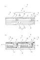
図1(a)に示す太陽電池モジュールI0は、共通の透光性基板10上に形成された複数の単位素子(セル)(Ia,Ib,Ic,・・・)を電気的に直列に接続した集積型構造(モジュール)を有する薄膜太陽電池である。図1(a)に示すように、太陽電池モジュールI0は、透光性基板10上に順に成膜された第1電極層としての透明電極層11、バッファー層12、化合物半導体からなる吸収層としての発電層13、第2電極層としての裏面電極層14を備えている。
<Solar cell module I 0>
FIG. 1 is a diagram illustrating an example of a solar cell module to which the present embodiment is applied.
Solar cell module I 0 shown in FIG. 1 (a), a plurality of unit elements formed on a common light transmissive substrate 10 (cell) (Ia, Ib, Ic, ···) electrically in series It is a thin film solar cell having a connected integrated structure (module). As shown in FIG. 1 (a), the solar cell module I 0 is the first transparent electrode layer as an
透明電極層11と裏面電極層14とは、それぞれ複数個に絶縁分離されている(透明電極層11a,11b,・・・/裏面電極層14a,14b,14c,・・・)。絶縁分離された透明電極層11(11a,11b,・・・)及び当該透明電極層11(11a,11b,・・・)にそれぞれ対向し、分離溝16によって絶縁分離された裏面電極層14(14a,14b,14c,・・・)と、これらの一対の電極層にそれぞれ挟まれたバッファー層12及び発電層13からなる複数のセル(Ia,Ib,Ic,・・・)が、互いに隣接する他のセルと電気的に直列に接続されている。
The
図1(a)に示すように、本実施の形態では、発電層13は、従来のスーパーストレート構造における化合物半導体層のように分割形成されておらず、複数の透明電極層11(11a,11b,・・・)上に連続的な膜として形成されている。そして、発電層13には、当該発電層13を構成する化合物半導体に含まれる元素の少なくとも一部を含み且つ当該発電層13の他の部分と比べ電気抵抗が低い短絡層15(・・・,15b,15c,・・・)が形成されている。
また、本実施の形態では、第2電極層としての裏面電極層14(14a,14b,14c,・・・)は、金属粉の集合体から形成されている。短絡層15(・・・,15b,15c,・・・)及び裏面電極層14(14a,14b,14c,・・・)については後述する。
As shown in FIG. 1A, in the present embodiment, the
Moreover, in this Embodiment, the back surface electrode layer 14 (14a, 14b, 14c, ...) as a 2nd electrode layer is formed from the aggregate | assembly of metal powder. The short-circuit layer 15 (..., 15b, 15c, ...) and the back electrode layer 14 (14a, 14b, 14c, ...) will be described later.
(太陽電池モジュールI0の構成要素)
(透光性基板10)
透光性基板10を構成する材料としては、例えば、透光性プラスチック材料、ガラス等が挙げられる。透光性プラスチック材料としては、例えば、ポリエチレンナフタレート、ポリカーボネート、ポリイミド、ポリエーテルサルホン、ポエイフェニレンスルフィド、フッ素樹脂等が挙げられる。透光性基板10の大きさは特に限定されない。本実施の形態では縦×横が8.5cm×8.5cmであり、厚さは、0.5mm程度である。
(Components of the solar cell module I 0)
(Translucent substrate 10)
As a material which comprises the translucent board |
(透明電極層11)
透明電極層11は、本実施の形態では、ITO(Indium Tin Oxide)、SnO2、ZnOから選択された少なくとも1つを含む金属材料を用い、スパッタリングまたは蒸着法により成膜することが好ましい。透明電極層11の厚さは、本実施の形態では、約0.6μmである。
(Transparent electrode layer 11)
In the present embodiment, the
(バッファー層12)
本実施の形態では、透明電極層11と発電層13との間にバッファー層12を設けている。バッファー層12を構成する材料は特に限定されないが、本実施の形態では、InS3、ZnS等の硫化物を使用している。透明電極層11と発電層13との間にバッファー層12を設けることにより、透明電極層11と発電層13との界面で発生する欠陥を抑制している。
(Buffer layer 12)
In the present embodiment, the
(発電層13)
発電層13を構成する化合物半導体は、例えば、周期表IB族、IIIB族、VIB族の元素を含むカルコパイライト型化合物半導体が挙げられる。本実施の形態では、銅(Cu)、インジウム(In)及びセレン(Se)を含むカルコパイライト構造を有するCu−In−Se系半導体材料により構成されることが好ましい。
(Power generation layer 13)
Examples of the compound semiconductor that constitutes the
ここで、発電層13を構成する材料としてCu−In−Se系半導体材料を採用する場合、透明電極層11側に、n型半導体を形成しやすいInとSeとの混合物からなるn型半導体形成用前駆体層を成膜し、次に、裏面電極層14側に、p型半導体を形成しやすいCuとSeとの混合物からなるp型半導体形成用前駆体層を成膜することが好ましい。この場合、p型半導体形成用前駆体層とn型半導体形成用前駆体層とが相互に溶融拡散することにより、良好な結晶性を有する発電層13が生成し、pn接合を形成される。
発電層13の厚さは、本実施の形態では、0.3μm〜5μmの範囲内である。
Here, when a Cu—In—Se based semiconductor material is adopted as a material constituting the
In the present embodiment, the thickness of the
(短絡層15)
短絡層15は、発電層13を構成する元素の一部を含み、且つ裏面電極層14と隣接する他のセルの透明電極層11とを電気的に短絡している。本実施の形態では、短絡層15には、発電層13を構成する化合物半導体の元素である周期表IB族、IIIB族、VIB族の元素が、発電層13とは異なる組成比で含まれている。
(Short-circuit layer 15)
The short-
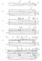
ここで、短絡層15に含まれる元素の組成比と電気的な抵抗率ρ(Ωcm)との関係について図4を用いて説明する。尚、図4は、平成元年度新エネルギー・産業技術総合開発機構委託業務成果報告書「新型太陽電池の実用化解析に関する調査研究II−化合物薄膜太陽電池−」第50頁から引用した。
Here, the relationship between the composition ratio of the elements contained in the short-
図4は、化合物半導体に含まれる(IB族元素/IIIB族元素)組成と抵抗率との関係を示すグラフである。図4において、横軸は、IB族元素のCu(銅)とIIIB族元素のIn(インジウム)との組成比(Cu/In)を表し、縦軸は、抵抗率ρ(Ωcm)を表す。図4に示すように、化合物半導体に含まれるCu元素とIn元素との組成比(Cu/In)が0.9以下の場合は、抵抗率ρ(Ωcm)が104Ωcm以上の高抵抗率を示す発電領域Aとなる。一方、Cu元素とIn元素との組成比(Cu/In)が1.15以上の場合は、抵抗率ρ(Ωcm)が約10−1Ωcm以下の低抵抗率を示す短絡領域Bとなる(ケミカルシャント)。この結果に従えば、IIIB族元素に対するIB族元素の割合を調整することにより、化合物半導体の抵抗率ρ(Ωcm)を化学的に調整することが可能となる。 FIG. 4 is a graph showing the relationship between the composition and the resistivity contained in the compound semiconductor (Group IB element / Group IIIB element). In FIG. 4, the horizontal axis represents the composition ratio (Cu / In) of the group IB element Cu (copper) and the group IIIB element In (indium), and the vertical axis represents the resistivity ρ (Ωcm). As shown in FIG. 4, when the composition ratio (Cu / In) between the Cu element and the In element contained in the compound semiconductor is 0.9 or less, the resistivity ρ (Ωcm) is 10 4 Ωcm or more. Is a power generation region A. On the other hand, when the composition ratio (Cu / In) between the Cu element and the In element is 1.15 or more, the short-circuit region B showing a low resistivity with a resistivity ρ (Ωcm) of about 10 −1 Ωcm or less is obtained ( Chemical shunt). According to this result, the resistivity ρ (Ωcm) of the compound semiconductor can be chemically adjusted by adjusting the ratio of the group IB element to the group IIIB element.
具体的には、本実施の形態では、短絡層15に含まれるIB族元素(Cu)とIIIB族元素(In)との比(Ib/IIIb)が1.15以上、好ましくは1.2以上となるように構成されている。短絡層15の製造方法については後述する。
尚、本実施の形態では、IB族元素として、Cu元素以外に銀(Ag)元素を使用することができる。周期表においてCu元素と同族(IB族)に属するAg元素は、Cu元素と同じ数の最外殻電子を有することから、Cu元素とIn元素との組成比(Cu/In)と同様に、Ag元素とIn元素との組成比(Ag/In)を調整することにより、化合物半導体の抵抗率ρ(Ωcm)を短絡領域Bにおける低抵抗率ρ(Ωcm)の範囲に調整することが可能となる。
Specifically, in the present embodiment, the ratio (Ib / IIIb) of the IB group element (Cu) and the IIIB group element (In) contained in the short-
In this embodiment, a silver (Ag) element can be used as the IB group element in addition to the Cu element. Since the Ag element belonging to the same group (IB group) as the Cu element in the periodic table has the same number of outermost electrons as the Cu element, similarly to the composition ratio (Cu / In) of the Cu element and the In element, By adjusting the composition ratio (Ag / In) of Ag element and In element, it is possible to adjust the resistivity ρ (Ωcm) of the compound semiconductor to the range of the low resistivity ρ (Ωcm) in the short-circuit region B. Become.
(裏面電極層14)
裏面電極層14は、金属粉の集合体から構成されている。ここで金属粉とは、金属元素の粒子を意味する。金属粉は、金属粒子または金属酸化物粒子を含み、それらは集団で金属粉を形成している。金属粉を用いると、例えばスクリーン印刷により裏面電極層14を形成することが可能である。スクリーン印刷により形成された裏面電極層14の金属粉の一部は発電層13に接触する。さらに、裏面電極層14中の金属粉同士が接触し、平面方向に電子が伝播する。
金属粉に含まれる金属元素としては、例えば、Mo、Ti、Cr、Al、Ag、Au、Cu及びPt等が挙げられる。また、これらの金属の合金も金属粒子として例示される。本実施の形態では、これらの中でも、銀(Ag)、銅(Cu)又はアルミニウム(Al)が好ましい。裏面電極層14は、上述した金属元素の粒子を含む金属粉分散液を使用する湿式成膜方法により、発電層13上に成膜される。裏面電極層14の成膜方法については後述する。
金属粉分散液に含まれる金属元素の粒径は、通常、数nm〜数μmの範囲から選択され、特に限定されない。本実施の形態では10μm以下が好ましい。また、例えば、厚さ1μm×長さ10μm程度の板状金属粉も使用可能である。
(Back electrode layer 14)
The
Examples of the metal element contained in the metal powder include Mo, Ti, Cr, Al, Ag, Au, Cu, and Pt. Moreover, alloys of these metals are also exemplified as metal particles. In the present embodiment, among these, silver (Ag), copper (Cu), or aluminum (Al) is preferable. The
The particle size of the metal element contained in the metal powder dispersion is usually selected from the range of several nm to several μm and is not particularly limited. In this embodiment, 10 μm or less is preferable. Further, for example, plate-like metal powder having a thickness of about 1 μm and a length of about 10 μm can be used.
図1(b)は、太陽電池モジュールI0における電子の流れを説明する図である。図中の直線状の矢印は、電子の流れを示す。図1(b)に示すように、スーパーストレート構造を有する太陽電池モジュールI0では、電子は、透光性基板10上に分割形成された透明電極層11(11a,11b,・・・)を流れ、発電層13の一部に形成された短絡層15(・・・15b,15c,・・・)を介して発電層13上に分離形成された裏面電極層14(14a,14b,14c,・・・)に流れる。この場合、分離溝16によって各セルの電子の流れが遮断される。これにより、第1のセルとしての単位セルIaの透明電極層11aと、第2のセルとしての単位セルIbの裏面電極層14bとが電気的に直列に接続される。
Figure 1 (b) is a diagram for explaining the electron flow in the solar cell module I 0. The straight arrows in the figure indicate the flow of electrons. As shown in FIG. 1 (b), the solar cell module I 0 having a superstrate structure, electrons,
前述したように、本実施の形態では、発電層13の一部に形成された短絡層15の抵抗率ρ(Ωcm)が約10−1Ωcm以下(化学的抵抗低下による短絡:ケミカルシャント)となるように調整されている。一方、発電層13の短絡層15以外の部分は、その抵抗率ρ(Ωcm)が104Ωcm以上(発電領域)となっている。
このため、本実施の形態が適用される太陽電池モジュールI0では、透明電極層11と裏面電極層14との接触部を形成することなく、透明電極層11内を流れる電子は、発電層13の一部に形成された短絡層15から隣接するセル中に流れる。これにより、メカニカルスクライブ工程により発電層13を分割することなく、複数のセル(Ia,Ib,Ic,・・・)を電気的に直列に接続した集積型構造(モジュール)を有する薄膜太陽電池が得られる。
As described above, in the present embodiment, the resistivity ρ (Ωcm) of the short-
Therefore, the solar cell module I 0 the present embodiment is applied, without forming a contact portion between the
このように、本実施の形態では、ケミカルシャントの原理を応用し、発電層13をメカニカルスクライブ工程により分割することなく、その一部に短絡層15を設けている。これにより、電子が裏面電極層14から透明電極層11内に流れるインターコネクト面積が拡大し、電気的に直列に接続した集積型構造(モジュール)の電気抵抗が低減する。
また、発電層13をメカニカルスクライブ工程により分割する必要がなく、量産性が向上するとともに、分割された発電層13の端面からの劣化が抑制される。
Thus, in this Embodiment, the principle of a chemical shunt is applied and the
Moreover, it is not necessary to divide the
<太陽電池モジュールI0の製造方法>
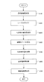
次に、太陽電池モジュールI0の製造方法を、図2及び図3を用いて説明する。
図2は、太陽電池モジュールI0の製造方法を説明するフローチャートである。図3は、太陽電池モジュールI0の製造方法の一例を説明する図である。図1と同じ構成については同じ符号を用い、その説明を省略する。
<Method of manufacturing a solar cell module I 0>
Next, a manufacturing method of the solar cell module I 0, will be described with reference to FIGS.
Figure 2 is a flowchart illustrating a method of manufacturing a solar cell module I 0. Figure 3 is a diagram illustrating an example of a method for manufacturing a solar cell module I 0. The same components as those in FIG.
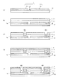
先ず、図3(a)に示すように、前述した材料からなる透光性基板10上に第1導電膜を連続的に成膜し(ステップ100:透明電極層成膜(第1導電膜成膜工程))、成膜した第1導電膜の一部をパターニングにより除去し(ステップ200:レーザスクライブ(パターニング工程))、複数に分割された透明電極層11(11a,11b)を形成する。第1導電膜の成膜方法は、スパッタリング法、MOCVD法等が挙げられる。本実施の形態では、スパッタリング法を採用している。本実施の形態では、パターニング工程は、例えば、ネオジウムYAGレーザ等の赤外領域(1,064nm)のビームを使用するレーザスクライブ法(LS)を採用している。
First, as shown in FIG. 3A, a first conductive film is continuously formed on the
次に、図3(b)に示すように、分割形成した透明電極層11(11a,11b)上にバッファー層12を成膜し、さらに、バッファー層12上に、IB族元素、IIIB族元素、VIB族元素を含む化合物半導体層130を成膜する(ステップ300:化合物半導体層成膜(化合物半導体層成膜工程))。
バッファー層12の成膜方法としては、スパッタリング法、化学溶液成長法等が挙げられる。本実施の形態では、化学溶液成長法等の湿式成膜を採用している。
Next, as shown in FIG. 3B, a
Examples of the method for forming the
本実施の形態では、化合物半導体層130は、複数のp型半導体形成用前駆体層とn型半導体形成用前駆体層とを積層させて成膜する。即ち、本実施の形態では、化合物半導体としてCu−In−Se系半導体材料を採用し、透明電極層11(11a,11b)側にn型半導体を形成しやすいInとSeとの混合物からなるn型半導体形成用前駆体層を成膜し、後述する裏面電極層14側にp型半導体を形成しやすいCuとSeとの混合物からなるp型半導体形成用前駆体層を成膜する。p型半導体形成用前駆体層とn型半導体形成用前駆体層とは、後述する加熱工程において相互に溶融拡散することにより、良好な結晶性を有する半導体からなる発電層13が生成し、pn接合を形成させることができる。
In the present embodiment, the
化合物半導体層130の成膜方法としては、例えば、真空蒸着法、気相セレン化法、スパッタリング法、ハイブリッドスパッタ法、湿式成膜法等が挙げられる。本実施の形態では、湿式成膜法を採用している。即ち、予め、化合物半導体であるp型半導体形成用前駆体とn型半導体形成用前駆体を含む所定の半導体分散液をそれぞれ調製し、塗布又は印刷等の手法によりバッファー層12上に前述した2種類の半導体形成用前駆体層を積層し、化合物半導体層130を成膜する。あるいは、2種類の前駆体粒子(例えば、Cu−Se粒子、およびIn−Se粒子)を混合した半導体分散液を1層以上成膜しても良い。各前駆体粒子のサイズは1μm以下、好ましくは200nm以下が良い。
Examples of the method for forming the
次に、図3(c)に示すように、化合物半導体層130の一部に、スクリーン印刷法により、少なくともIB族元素を含む導電性ペースト層150を形成する(ステップ400:導電性ペースト塗布(導電性ペースト層形成工程))。
ここで、導電性ペースト層150を構成する導電性ペーストとしては、通常、熱可塑性ポリエステル樹脂、アクリル樹脂、エポキシ樹脂等の樹脂をバインダとし、これに銀、銅、アルミニウム等の金属の微粉末やカーボンブラック等の導電性微粉末を添加し、種々の有機溶媒にこれらバインダ、導電性微粒子を溶解、分散させて調製されたものとして定義される。金属の微粉末としては、例えば、銅粒子、ニッケル粒子、アルミニウム粒子等の表面の一部が、例えば、銀、金等の他の金属で被覆された複合金属粉も使用される。また、中でも銀については、例えば、酸化第1銀、酸化第2銀、炭酸銀、酢酸銀、アセチルアセトン銀錯体等の粒子状銀化合物が好ましい。
このような導電性ペーストとしては、市販されている従来公知のものを使用することができる。本実施の形態では、例えば、藤倉化成株式会社製Agペースト:ドータイトXA−9053を使用している。
Next, as shown in FIG. 3C, a
Here, as the conductive paste constituting the
As such a conductive paste, a conventionally known paste that is commercially available can be used. In the present embodiment, for example, Ag paste: Dotite XA-9053 manufactured by Fujikura Kasei Co., Ltd. is used.
続いて、図3(d)に示すように、導電性ペースト層150が形成された化合物半導体層130を加熱し、化合物半導体の結晶からなる発電層13を形成すると共に、導電性ペースト層150に含まれるIB族元素を化合物半導体層130に拡散させ、後述する裏面電極層14(14a,14b,14c)と透明電極層11(11a,11b)とを短絡する短絡層15(15b,15c)を形成する(ステップ500:化合物半導体加熱(第1加熱工程))。
化合物半導体層130を加熱する温度は、本実施の形態では300℃以上、好ましくは350℃、さらに好ましくは600℃以下、特に好ましくは550℃以下である。
Subsequently, as shown in FIG. 3D, the
In this embodiment mode, the temperature at which the
このような第1加熱工程において、化合物半導体層130のp型半導体形成用前駆体層とn型半導体形成用前駆体層とは相互に相互拡散することにより、良好な結晶性を有する半導体からなる発電層13が生成する。また、複数の前駆体粒子を混合した半導体分散液の塗膜を加熱することにより、複数の前駆体粒子が相互拡散し、良好な結晶性を有する半導体からなる発電層13が得られる。
この場合、半導体層はp型となるが、バッファー層12から、半導体層中に、半導体層をn型に変えるZn、Cd等のIIB族元素が拡散し、pn接合が形成される。この際、バッファー層12から半導体層中にIIB族元素が過度に拡散しないように、予めIIB族元素の遊離しやすさを制御する必要がある。例えば、バッファー層12に一般的に使用されるIIB族元素の主要化合物としては、硫化物が挙げられる。また、硫化物より結合が強くIIB族元素の熱的安定性が高い酸化物を用いることができる。さらに、酸化物と硫化物の複合金属カルコゲナイドを使用しても良い。
In the first heating step, the p-type semiconductor forming precursor layer and the n-type semiconductor forming precursor layer of the
In this case, although the semiconductor layer is p-type, IIB group elements such as Zn and Cd that change the semiconductor layer to n-type diffuse from the
さらに、導電性ペースト層150に含まれるCu元素やAg元素等のIB族元素が金属イオンとして化合物半導体層130に拡散することにより、化合物半導体層130に導電性ペーストが拡散した部分のみ、IB族元素の組成比が増大する。その結果、化合物半導体層130に含まれるIB族元素とIIIB族元素との組成(IB族元素/IIIB族元素)が、低抵抗率を得る範囲(図4に示す短絡領域B)にシフトし、抵抗率ρ(Ωcm)が約10−1Ωcm以下(ケミカルシャント)の短絡層15(15b,15c)が形成される。
Furthermore, IB group elements such as Cu element and Ag element contained in the
続いて、図3(e)に示すように、全体として透明電極層11(11a,11b)を覆う連続膜として形成され且つ電気抵抗が低い短絡層15(15b,15c)が設けられている発電層13上に、湿式成膜法により、絶縁分離された複数の第2導電膜としての裏面電極層14(14a,14b,14c)を成膜する(ステップ600:裏面電極層印刷(第2導電膜成膜工程))。
本実施の形態において、「第2導電膜成膜工程」とは、メカニカルスクライブにより裏面電極層を分割すべき部分が印刷されないように(即ち、分離溝16を形成するように)、スクリーン印刷等の手法により絶縁分離した複数の裏面電極層14(14a,14b,14c)を成膜することを意味する。これにより、従来技術において裏面電極層を分割するメカニカルスクライブ工程が不要となる。さらに、スクリーン印刷等の湿式成膜方法は、真空を必要としないので、真空成膜工程を削減することができる。
Subsequently, as shown in FIG. 3 (e), the power generation is provided as a continuous film covering the transparent electrode layer 11 (11a, 11b) as a whole and provided with a short-circuit layer 15 (15b, 15c) having a low electrical resistance. On the
In the present embodiment, the “second conductive film forming step” refers to screen printing or the like so that the portion where the back electrode layer is to be divided is not printed by mechanical scribing (that is, the
本実施の形態において、裏面電極層14(14a,14b,14c)を成膜する際に使用する金属粉分散液は、所定の流動性を有する分散媒又は分散剤(以下、「分散媒等」と記す)と分散媒等中に分散する金属粉(金属元素の粒子)を含んでいる。金属粉分散液中に含まれる金属粉は前述した通りである。本実施の形態では、金属粉の金属元素としては、銀(Ag)、銅(Cu)又はアルミニウム(Al)が好ましい。金属粉分散液の種類としては、例えば、溶液、コロイド、懸濁液等が挙げられる。
湿式成膜法としては、印刷が挙げられる。具体的には、インクジェット印刷、空気圧式噴霧、スクリーン印刷、パッド印刷、レーザ印刷、ドットマトリックス印刷、感熱式印刷、リソグラフィ等が挙げられる。本実施の形態では、スクリーン印刷を採用し、発電層13上に絶縁分離した複数の裏面電極層14(14a,14b,14c)を成膜している。これにより、金属粉分散液中に含まれる金属粉の集合体からなる裏面電極層14(14a,14b,14c)が形成される。
In the present embodiment, the metal powder dispersion used for forming the back electrode layer 14 (14a, 14b, 14c) is a dispersion medium or dispersant having a predetermined fluidity (hereinafter referred to as "dispersion medium"). And metal powder (metal element particles) dispersed in a dispersion medium or the like. The metal powder contained in the metal powder dispersion is as described above. In the present embodiment, silver (Ag), copper (Cu), or aluminum (Al) is preferable as the metal element of the metal powder. Examples of the metal powder dispersion include solutions, colloids, and suspensions.
Examples of the wet film forming method include printing. Specific examples include inkjet printing, pneumatic spraying, screen printing, pad printing, laser printing, dot matrix printing, thermal printing, lithography, and the like. In the present embodiment, screen printing is employed, and a plurality of back electrode layers 14 (14 a, 14 b, 14 c) that are insulated and separated are formed on the
本実施の形態が適用される太陽電池モジュールI0において、金属粉の集合体からなる裏面電極層14(14a,14b,14c)は、従来、スパッタリング等の真空成膜法により成膜した導電膜と比較して、透光性基板10側から発電層13に入射する入射光を反射する反射層としての機能が増大することが期待できる。さらに、後述するように、裏面電極層14(14a,14b,14c)の外側に塗布するエチレン−酢酸ビニル樹脂(EVA樹脂)との接着性が改良されると考えられる。
尚、本実施の形態では、前述した導電性ペースト層150を形成する際に使用する導電性ペーストを使用し、スクリーン印刷により、発電層13上に絶縁分離された複数の裏面電極層14(14a,14b,14c)を成膜することも可能である。
In the solar cell module I 0 which this embodiment is applied, the metal powder of the assembly back
In the present embodiment, the plurality of back electrode layers 14 (14a) that are insulated and separated on the
次に、発電層13上に塗布された複数の裏面電極層14(14a,14b,14c)を加熱乾燥し、成膜工程で使用した金属粉分散液中の分散媒を除去する(ステップ700:裏面電極層加熱(第2加熱工程))。本実施の形態では、加熱温度は、100℃以上であり、好ましくは150℃以上であり、さらに好ましくは250℃以下であり、特に好ましくは200℃以下である。
Next, the plurality of back electrode layers 14 (14a, 14b, 14c) applied on the
最後に、図3(f)に示すように、スーパーストレート構造に形成された太陽電池モジュールI0の裏面電極層14(14a,14b,14c)側にエチレン−酢酸ビニル樹脂(EVA樹脂)を塗布し、さらにバックシートを載せて加熱圧着する。
Finally, as shown in FIG. 3 (f), the
上述したように、本実施の形態では、短絡層15(15b,15c)は発電層13とバッファー層12に拡散し透明電極層11(11a,11b)に達することにより、裏面電極層14(14a,14b,14c)と透明電極層11(11a,11b)とを電気的に短絡させている。本実施の形態が適用される太陽電池モジュールI0の製造方法は、従来から行われているCIS薄膜太陽電池の製造工程と比べ、真空成膜工程を採用することなく、大気圧においてバッファー層12と発電層13と裏面電極層14(14a,14b,14c)とが連続的に一貫成膜できる。また、従来、発電層13と裏面電極層14(14a,14b,14c)を分割するメカニカルスクライブ工程を採用する必要がない。このため、化合物半導体を含む発電層13が大気に暴露される機会が低減し、太陽電池の性能低下が防止される。また、通常、長時間を要するメカニカルスクライブ工程を削減することにより量産性の低下を防ぐことができる。さらに、メカニカルスクライブ後に生じる切削された端面からの劣化が抑制される。
As described above, in the present embodiment, the short-circuit layer 15 (15b, 15c) diffuses into the
また、本実施の形態が適用される太陽電池モジュールI0は、裏面電極層14(14a,14b,14c)と透明電極層11(11a,11b)とを電気的に短絡させる短絡層15(15b,15c)を設けることにより、透明電極層11(11a,11b)の厚さを薄くすることが可能となり、製造コストの低減と共に、光透過率の向上及び発電効率の増大が期待できる。即ち、従来の集積型の太陽電池モジュールでは、インターコネクトの抵抗を低下させるために、変換効率の低下をある程度犠牲にして、透明電極層を厚く形成する必要があった。しかし、本実施の形態における太陽電池モジュールI0のように、化合物半導体層130の導電性ペーストが塗布された部分のみに、IB族元素とIIIB族元素との組成が、低抵抗率が得られる範囲にシフトした短絡層15(15b,15c)を設けることにより、上述した問題が解決される。
Further, the solar cell module I 0 which this embodiment is applied, the back electrode layer 14 (14a, 14b, 14c) and the transparent electrode layer 11 (11a, 11b)
尚、以上の説明は、本発明の実施の形態を説明するための一例に過ぎず、本発明は本実施の形態に限定されるものではない。
本発明は複数の元素から構成される半導体層と、これを挟む2つの電極層を備える太陽電池モジュールや、このような構造を有する太陽電池モジュールの製造方法に応用することができる。例えば、Cd−Te系に代表されるIII−V族半導体、Cu−In−Se系に代表されるI−III−VI族半導体、Cu−Zn−Sn−S系化合物に代表されるI−II−IV−VI族半導体、II−IV−V族半導体、Si−Ge系等の2種類以上の元素からなるIV族半導体に適用することも可能である。
In addition, the above description is only an example for demonstrating embodiment of this invention, and this invention is not limited to this embodiment.
The present invention can be applied to a solar cell module including a semiconductor layer composed of a plurality of elements and two electrode layers sandwiching the semiconductor layer, and a method for manufacturing a solar cell module having such a structure. For example, a III-V group semiconductor typified by a Cd-Te system, an I-III-VI group semiconductor typified by a Cu-In-Se system, and an I-II typified by a Cu-Zn-Sn-S system compound The present invention can also be applied to an IV group semiconductor composed of two or more elements such as an -IV-VI group semiconductor, an II-IV-V group semiconductor, and a Si-Ge group.
1,1a,1b,11,11a,11b…透明電極層、2,12…バッファー層、3,13…発電層、4,14,14a,14b,14c…裏面電極層、10…透光性基板、15,15b,15c…短絡層、16…分離溝、I0…太陽電池モジュール 1, 1a, 1b, 11, 11a, 11b ... Transparent electrode layer, 2, 12 ... Buffer layer, 3, 13 ... Power generation layer, 4, 14, 14a, 14b, 14c ... Back electrode layer, 10 ... Translucent substrate , 15 and 15b, 15c ... shorting layer, 16 ... separation groove, I 0 ... solar cell module
Claims (18)
前記第1電極層と前記第2電極層とは、それぞれ複数個に絶縁分離され、
分離された一つの前記第1電極層と当該第1電極層と対向する前記第2電極層、当該第1電極層及び当該第2電極層に挟まれた前記吸収層からなる一つのセルが、隣接する他のセルと電気的に直列に接続され、
前記第2電極層は、金属粉の集合体からなる
ことを特徴とする太陽電池モジュール。 A solar cell module comprising a first electrode layer, an absorption layer, and a second electrode layer sequentially formed on a light-transmitting substrate,
The first electrode layer and the second electrode layer are each insulated and separated into a plurality of pieces,
One cell composed of the separated first electrode layer and the second electrode layer facing the first electrode layer, the first electrode layer, and the absorption layer sandwiched between the second electrode layers, Electrically connected in series with other adjacent cells,
The said 2nd electrode layer consists of an aggregate | assembly of metal powder, The solar cell module characterized by the above-mentioned.
前記セルは、
透光性基板上に形成された第1電極層と、
前記第1電極層上に直接又は他の層を介して成膜された吸収層と、
前記吸収層上に金属粉の集合体により成膜された第2電極層と、
を有することを特徴とする太陽電池モジュール。 A solar cell module in which a plurality of cells are electrically connected in series,
The cell is
A first electrode layer formed on the translucent substrate;
An absorption layer formed directly or via another layer on the first electrode layer;
A second electrode layer formed of a metal powder aggregate on the absorption layer;
A solar cell module comprising:
透光性基板上に透光性の第1導電膜を成膜する第1導電膜成膜工程と、
成膜された前記第1導電膜の一部を除去し絶縁分離された複数の第1電極層を形成するパターニング工程と、
分離形成された複数の前記第1電極層上にIB族元素、IIIB族元素、VIB族元素を含む化合物半導体層を成膜する化合物半導体層成膜工程と、
成膜された前記化合物半導体層上の一部に少なくともIB族元素を含む導電性ペースト層を形成する導電性ペースト層形成工程と、
成膜された前記化合物半導体層を加熱し、化合物半導体の結晶からなる吸収層を形成すると共に、前記導電性ペースト層に含まれるIB族元素を当該吸収層内に拡散させ、当該吸収層の他の部分と比べ電気抵抗が低い短絡層を形成する第1加熱工程と、
成膜された前記吸収層上に、湿式成膜法を用い、分離された複数の第2導電膜を成膜する第2導電膜成膜工程と、
分離成膜された複数の前記第2導電膜を加熱し絶縁分離された複数の第2電極層を形成するとともに前記第1電極層と当該第2電極層とを、前記短絡層を介して電気的に直列接続させる第2加熱工程と、
を有することを特徴とする太陽電池モジュールの製造方法。 A method for manufacturing a solar cell module, comprising:
A first conductive film forming step of forming a light-transmitting first conductive film on a light-transmitting substrate;
A patterning step of removing a part of the formed first conductive film to form a plurality of first electrode layers that are insulated and separated;
A compound semiconductor layer film forming step of forming a compound semiconductor layer containing a group IB element, a group IIIB element, and a group VIB element on the plurality of first electrode layers formed separately;
A conductive paste layer forming step of forming a conductive paste layer containing at least a group IB element on a part of the compound semiconductor layer formed;
The formed compound semiconductor layer is heated to form an absorption layer made of a compound semiconductor crystal, and a group IB element contained in the conductive paste layer is diffused into the absorption layer, so that the other absorption layer is formed. A first heating step for forming a short-circuit layer having a lower electrical resistance than that of
A second conductive film forming step of forming a plurality of separated second conductive films on the formed absorption layer using a wet film forming method;
The plurality of second conductive films formed separately are heated to form a plurality of second electrode layers that are insulated and separated, and the first electrode layer and the second electrode layer are electrically connected via the short-circuit layer. A second heating step for serial connection,
The manufacturing method of the solar cell module characterized by having.
Priority Applications (1)
| Application Number | Priority Date | Filing Date | Title |
|---|---|---|---|
| JP2011054676A JP2012191069A (en) | 2011-03-11 | 2011-03-11 | Solar cell module, manufacturing method therefor |
Applications Claiming Priority (1)
| Application Number | Priority Date | Filing Date | Title |
|---|---|---|---|
| JP2011054676A JP2012191069A (en) | 2011-03-11 | 2011-03-11 | Solar cell module, manufacturing method therefor |
Publications (1)
| Publication Number | Publication Date |
|---|---|
| JP2012191069A true JP2012191069A (en) | 2012-10-04 |
Family
ID=47083895
Family Applications (1)
| Application Number | Title | Priority Date | Filing Date |
|---|---|---|---|
| JP2011054676A Withdrawn JP2012191069A (en) | 2011-03-11 | 2011-03-11 | Solar cell module, manufacturing method therefor |
Country Status (1)
| Country | Link |
|---|---|
| JP (1) | JP2012191069A (en) |
Cited By (2)
| Publication number | Priority date | Publication date | Assignee | Title |
|---|---|---|---|---|
| JP2018026539A (en) * | 2016-08-03 | 2018-02-15 | パナソニック株式会社 | Solar cell module and manufacturing method thereof |
| WO2025197949A1 (en) * | 2024-03-19 | 2025-09-25 | 富士フイルム株式会社 | Method for manufacturing solar cell |
-
2011
- 2011-03-11 JP JP2011054676A patent/JP2012191069A/en not_active Withdrawn
Cited By (2)
| Publication number | Priority date | Publication date | Assignee | Title |
|---|---|---|---|---|
| JP2018026539A (en) * | 2016-08-03 | 2018-02-15 | パナソニック株式会社 | Solar cell module and manufacturing method thereof |
| WO2025197949A1 (en) * | 2024-03-19 | 2025-09-25 | 富士フイルム株式会社 | Method for manufacturing solar cell |
Similar Documents
| Publication | Publication Date | Title |
|---|---|---|
| US20170271622A1 (en) | High efficiency thin film tandem solar cells and other semiconductor devices | |
| CN106876503B (en) | Using the solar energy stacked wafer moudle of center convergence gate line electrode | |
| CN103797585B (en) | Thin-film solar module with series connection and method for series connection of thin-film solar cells | |
| CN102598301A (en) | Solar cell and manufacturing method thereof | |
| CN107112376A (en) | Double-deck photovoltaic apparatus | |
| JP4394366B2 (en) | Double-sided solar cell | |
| CN102576762A (en) | Photovoltaic system and method of manufacturing the same | |
| CN103548151A (en) | Semiconductor device, solar cell module, solar cell string, and solar cell array | |
| US20150059838A1 (en) | Solar cell apparatus and method of fabricating the same | |
| JP2009004683A (en) | Integrated solar cell | |
| KR102122567B1 (en) | Flexible Thin Film Solar Cell With Extension Capability And Method For The Same | |
| US20150255659A1 (en) | Solar module | |
| JP5624153B2 (en) | Solar cell and manufacturing method thereof | |
| JP2012191069A (en) | Solar cell module, manufacturing method therefor | |
| JP2014232764A (en) | Solar cell | |
| KR101474487B1 (en) | Thin film solar cell and Method of fabricating the same | |
| KR20120086217A (en) | Solar cell apparatus and method of fabricating the same | |
| KR101173418B1 (en) | Solar cell and method of fabricating the same | |
| KR101919611B1 (en) | Transparent thin film solar cell including with a submicrometer sized absorber layer and manufacturing method for the same | |
| JP2012191137A (en) | Solar cell module, manufacturing method therefor | |
| JP2010251430A (en) | Integrated photovoltaic device and manufacturing method of integrated photovoltaic device | |
| JP2016171186A (en) | Photoelectric conversion device | |
| JP2012160511A (en) | Photoelectric conversion device | |
| JP2010114147A (en) | Integrated type light power generating element and method of manufacturing the same | |
| US9349901B2 (en) | Solar cell apparatus and method of fabricating the same |
Legal Events
| Date | Code | Title | Description |
|---|---|---|---|
| A300 | Application deemed to be withdrawn because no request for examination was validly filed |
Free format text: JAPANESE INTERMEDIATE CODE: A300 Effective date: 20140513 |