JP2012175103A - Optical apparatus, method of scanning, lithographic apparatus and device manufacturing method - Google Patents
Optical apparatus, method of scanning, lithographic apparatus and device manufacturing method Download PDFInfo
- Publication number
- JP2012175103A JP2012175103A JP2012027606A JP2012027606A JP2012175103A JP 2012175103 A JP2012175103 A JP 2012175103A JP 2012027606 A JP2012027606 A JP 2012027606A JP 2012027606 A JP2012027606 A JP 2012027606A JP 2012175103 A JP2012175103 A JP 2012175103A
- Authority
- JP
- Japan
- Prior art keywords
- radiation
- substrate
- mirror
- mark
- objective lens
- Prior art date
- Legal status (The legal status is an assumption and is not a legal conclusion. Google has not performed a legal analysis and makes no representation as to the accuracy of the status listed.)
- Granted
Links
- 230000003287 optical effect Effects 0.000 title claims abstract description 75
- 238000000034 method Methods 0.000 title claims description 37
- 238000004519 manufacturing process Methods 0.000 title claims description 10
- 239000000758 substrate Substances 0.000 claims abstract description 119
- 230000005855 radiation Effects 0.000 claims abstract description 78
- 238000005259 measurement Methods 0.000 claims abstract description 50
- 238000005286 illumination Methods 0.000 claims abstract description 45
- 210000001747 pupil Anatomy 0.000 claims abstract description 27
- 238000000059 patterning Methods 0.000 claims description 27
- 238000012545 processing Methods 0.000 claims description 20
- 230000008569 process Effects 0.000 claims description 15
- 238000001514 detection method Methods 0.000 claims description 10
- 238000012546 transfer Methods 0.000 claims description 9
- 230000008859 change Effects 0.000 claims description 8
- 238000001459 lithography Methods 0.000 claims description 7
- 238000007689 inspection Methods 0.000 claims description 3
- 230000007246 mechanism Effects 0.000 abstract description 7
- 239000011295 pitch Substances 0.000 description 13
- 239000010410 layer Substances 0.000 description 9
- 230000002829 reductive effect Effects 0.000 description 7
- 238000013461 design Methods 0.000 description 5
- 238000010586 diagram Methods 0.000 description 5
- 230000008901 benefit Effects 0.000 description 4
- 238000004590 computer program Methods 0.000 description 4
- 239000007788 liquid Substances 0.000 description 4
- 238000009826 distribution Methods 0.000 description 3
- 230000000694 effects Effects 0.000 description 3
- 230000006870 function Effects 0.000 description 3
- 238000007654 immersion Methods 0.000 description 3
- 239000000463 material Substances 0.000 description 3
- 238000000691 measurement method Methods 0.000 description 3
- 230000010363 phase shift Effects 0.000 description 3
- 230000003068 static effect Effects 0.000 description 3
- 238000004624 confocal microscopy Methods 0.000 description 2
- 230000009977 dual effect Effects 0.000 description 2
- 230000005670 electromagnetic radiation Effects 0.000 description 2
- 230000006872 improvement Effects 0.000 description 2
- 239000011159 matrix material Substances 0.000 description 2
- 238000012986 modification Methods 0.000 description 2
- 230000004048 modification Effects 0.000 description 2
- 238000000206 photolithography Methods 0.000 description 2
- 230000001360 synchronised effect Effects 0.000 description 2
- 238000012876 topography Methods 0.000 description 2
- XUIMIQQOPSSXEZ-UHFFFAOYSA-N Silicon Chemical compound [Si] XUIMIQQOPSSXEZ-UHFFFAOYSA-N 0.000 description 1
- 238000004458 analytical method Methods 0.000 description 1
- 238000003491 array Methods 0.000 description 1
- 238000000429 assembly Methods 0.000 description 1
- 230000000712 assembly Effects 0.000 description 1
- 230000002238 attenuated effect Effects 0.000 description 1
- 238000004364 calculation method Methods 0.000 description 1
- 238000004891 communication Methods 0.000 description 1
- 238000012937 correction Methods 0.000 description 1
- 238000013500 data storage Methods 0.000 description 1
- 230000001066 destructive effect Effects 0.000 description 1
- 230000005672 electromagnetic field Effects 0.000 description 1
- 238000010894 electron beam technology Methods 0.000 description 1
- 230000017525 heat dissipation Effects 0.000 description 1
- 238000003384 imaging method Methods 0.000 description 1
- 230000002452 interceptive effect Effects 0.000 description 1
- 238000010884 ion-beam technique Methods 0.000 description 1
- 239000002346 layers by function Substances 0.000 description 1
- 230000000670 limiting effect Effects 0.000 description 1
- 239000004973 liquid crystal related substance Substances 0.000 description 1
- 230000005381 magnetic domain Effects 0.000 description 1
- 238000013507 mapping Methods 0.000 description 1
- 239000003550 marker Substances 0.000 description 1
- 230000015654 memory Effects 0.000 description 1
- QSHDDOUJBYECFT-UHFFFAOYSA-N mercury Chemical compound [Hg] QSHDDOUJBYECFT-UHFFFAOYSA-N 0.000 description 1
- 229910052753 mercury Inorganic materials 0.000 description 1
- 239000000203 mixture Substances 0.000 description 1
- 239000013307 optical fiber Substances 0.000 description 1
- 239000002245 particle Substances 0.000 description 1
- 230000002093 peripheral effect Effects 0.000 description 1
- 230000010287 polarization Effects 0.000 description 1
- 238000002360 preparation method Methods 0.000 description 1
- 230000000750 progressive effect Effects 0.000 description 1
- 230000009467 reduction Effects 0.000 description 1
- 230000003252 repetitive effect Effects 0.000 description 1
- 230000004044 response Effects 0.000 description 1
- 230000011218 segmentation Effects 0.000 description 1
- 239000004065 semiconductor Substances 0.000 description 1
- 230000035945 sensitivity Effects 0.000 description 1
- 238000007493 shaping process Methods 0.000 description 1
- 229910052710 silicon Inorganic materials 0.000 description 1
- 239000010703 silicon Substances 0.000 description 1
- 238000001228 spectrum Methods 0.000 description 1
- 239000010409 thin film Substances 0.000 description 1
- XLYOFNOQVPJJNP-UHFFFAOYSA-N water Substances O XLYOFNOQVPJJNP-UHFFFAOYSA-N 0.000 description 1
Images


Classifications
-
- H—ELECTRICITY
- H01—ELECTRIC ELEMENTS
- H01L—SEMICONDUCTOR DEVICES NOT COVERED BY CLASS H10
- H01L21/00—Processes or apparatus adapted for the manufacture or treatment of semiconductor or solid state devices or of parts thereof
- H01L21/02—Manufacture or treatment of semiconductor devices or of parts thereof
- H01L21/027—Making masks on semiconductor bodies for further photolithographic processing not provided for in group H01L21/18 or H01L21/34
- H01L21/0271—Making masks on semiconductor bodies for further photolithographic processing not provided for in group H01L21/18 or H01L21/34 comprising organic layers
- H01L21/0273—Making masks on semiconductor bodies for further photolithographic processing not provided for in group H01L21/18 or H01L21/34 comprising organic layers characterised by the treatment of photoresist layers
-
- G—PHYSICS
- G02—OPTICS
- G02B—OPTICAL ELEMENTS, SYSTEMS OR APPARATUS
- G02B21/00—Microscopes
- G02B21/0004—Microscopes specially adapted for specific applications
- G02B21/002—Scanning microscopes
- G02B21/0024—Confocal scanning microscopes (CSOMs) or confocal "macroscopes"; Accessories which are not restricted to use with CSOMs, e.g. sample holders
- G02B21/0036—Scanning details, e.g. scanning stages
- G02B21/0048—Scanning details, e.g. scanning stages scanning mirrors, e.g. rotating or galvanomirrors, MEMS mirrors
-
- G—PHYSICS
- G01—MEASURING; TESTING
- G01B—MEASURING LENGTH, THICKNESS OR SIMILAR LINEAR DIMENSIONS; MEASURING ANGLES; MEASURING AREAS; MEASURING IRREGULARITIES OF SURFACES OR CONTOURS
- G01B11/00—Measuring arrangements characterised by the use of optical techniques
-
- G—PHYSICS
- G01—MEASURING; TESTING
- G01B—MEASURING LENGTH, THICKNESS OR SIMILAR LINEAR DIMENSIONS; MEASURING ANGLES; MEASURING AREAS; MEASURING IRREGULARITIES OF SURFACES OR CONTOURS
- G01B11/00—Measuring arrangements characterised by the use of optical techniques
- G01B11/14—Measuring arrangements characterised by the use of optical techniques for measuring distance or clearance between spaced objects or spaced apertures
-
- G—PHYSICS
- G02—OPTICS
- G02B—OPTICAL ELEMENTS, SYSTEMS OR APPARATUS
- G02B26/00—Optical devices or arrangements for the control of light using movable or deformable optical elements
- G02B26/08—Optical devices or arrangements for the control of light using movable or deformable optical elements for controlling the direction of light
- G02B26/10—Scanning systems
- G02B26/105—Scanning systems with one or more pivoting mirrors or galvano-mirrors
-
- G—PHYSICS
- G03—PHOTOGRAPHY; CINEMATOGRAPHY; ANALOGOUS TECHNIQUES USING WAVES OTHER THAN OPTICAL WAVES; ELECTROGRAPHY; HOLOGRAPHY
- G03F—PHOTOMECHANICAL PRODUCTION OF TEXTURED OR PATTERNED SURFACES, e.g. FOR PRINTING, FOR PROCESSING OF SEMICONDUCTOR DEVICES; MATERIALS THEREFOR; ORIGINALS THEREFOR; APPARATUS SPECIALLY ADAPTED THEREFOR
- G03F7/00—Photomechanical, e.g. photolithographic, production of textured or patterned surfaces, e.g. printing surfaces; Materials therefor, e.g. comprising photoresists; Apparatus specially adapted therefor
- G03F7/70—Microphotolithographic exposure; Apparatus therefor
- G03F7/70483—Information management; Active and passive control; Testing; Wafer monitoring, e.g. pattern monitoring
- G03F7/70605—Workpiece metrology
- G03F7/70616—Monitoring the printed patterns
- G03F7/70625—Dimensions, e.g. line width, critical dimension [CD], profile, sidewall angle or edge roughness
-
- G—PHYSICS
- G03—PHOTOGRAPHY; CINEMATOGRAPHY; ANALOGOUS TECHNIQUES USING WAVES OTHER THAN OPTICAL WAVES; ELECTROGRAPHY; HOLOGRAPHY
- G03F—PHOTOMECHANICAL PRODUCTION OF TEXTURED OR PATTERNED SURFACES, e.g. FOR PRINTING, FOR PROCESSING OF SEMICONDUCTOR DEVICES; MATERIALS THEREFOR; ORIGINALS THEREFOR; APPARATUS SPECIALLY ADAPTED THEREFOR
- G03F9/00—Registration or positioning of originals, masks, frames, photographic sheets or textured or patterned surfaces, e.g. automatically
- G03F9/70—Registration or positioning of originals, masks, frames, photographic sheets or textured or patterned surfaces, e.g. automatically for microlithography
- G03F9/7088—Alignment mark detection, e.g. TTR, TTL, off-axis detection, array detector, video detection
-
- H—ELECTRICITY
- H01—ELECTRIC ELEMENTS
- H01L—SEMICONDUCTOR DEVICES NOT COVERED BY CLASS H10
- H01L21/00—Processes or apparatus adapted for the manufacture or treatment of semiconductor or solid state devices or of parts thereof
- H01L21/02—Manufacture or treatment of semiconductor devices or of parts thereof
- H01L21/027—Making masks on semiconductor bodies for further photolithographic processing not provided for in group H01L21/18 or H01L21/34
- H01L21/0271—Making masks on semiconductor bodies for further photolithographic processing not provided for in group H01L21/18 or H01L21/34 comprising organic layers
- H01L21/0273—Making masks on semiconductor bodies for further photolithographic processing not provided for in group H01L21/18 or H01L21/34 comprising organic layers characterised by the treatment of photoresist layers
- H01L21/0274—Photolithographic processes
Landscapes
- Physics & Mathematics (AREA)
- General Physics & Mathematics (AREA)
- Engineering & Computer Science (AREA)
- Optics & Photonics (AREA)
- Chemical & Material Sciences (AREA)
- Multimedia (AREA)
- Analytical Chemistry (AREA)
- Manufacturing & Machinery (AREA)
- Microelectronics & Electronic Packaging (AREA)
- Power Engineering (AREA)
- Computer Hardware Design (AREA)
- Condensed Matter Physics & Semiconductors (AREA)
- Exposure And Positioning Against Photoresist Photosensitive Materials (AREA)
- Length Measuring Devices By Optical Means (AREA)
- Exposure Of Semiconductors, Excluding Electron Or Ion Beam Exposure (AREA)
Abstract
Description
[0001] 本発明は、光学装置、オブジェクトを放射ビームでスキャンする方法、リソグラフィ装置、及びデバイス製造方法に関する。本発明は、リソグラフィ装置で使用される測定方法を、これに限定されないが含む、測定方法に適用できる。 The present invention relates to an optical apparatus, a method for scanning an object with a radiation beam, a lithographic apparatus, and a device manufacturing method. The present invention is applicable to measurement methods including, but not limited to, measurement methods used in lithographic apparatus.
[0002] オブジェクトを光学的にスキャンする能力は多くの用途で有用である。「光学的にスキャンする」という表現は、オブジェクトのある地点に放射を照明し及び/又はそこからの放射を検出する一方で、オブジェクトを横切る1つ又は複数の方向に上記地点をスキャンすることを意味する。光学スキャンの用途の例は、関連出願US61444373号(den Boef他)に記載されているリソグラフィ装置のための新規のアライメントセンサでの使用である。別の用途の例は共焦顕微鏡である。 [0002] The ability to optically scan an object is useful in many applications. The expression “optically scan” refers to scanning the point in one or more directions across the object while illuminating and / or detecting the radiation at a point on the object. means. An example of an optical scanning application is the use in a novel alignment sensor for a lithographic apparatus described in the related application US Pat. No. 6,144,373 (den Boef et al.). Another example application is a confocal microscope.
[0003] リソグラフィ装置は、所望のパターンを基板に、通常は基板のターゲット部分に適用する機械である。リソグラフィ装置は、例えば、集積回路(IC)の製造に使用可能である。このような場合、代替的にマスク又はレチクルとも呼ばれるパターニングデバイスを使用して、ICの個々の層上に形成すべき回路パターンを生成することができる。このパターンを、基板(例えばシリコンウェーハ)上のターゲット部分(例えば1つ又は幾つかのダイの一部を含む)に転写することができる。パターンの転写は通常、基板に設けた放射感応性材料(レジスト)の層への結像により行われる。一般的に、1枚の基板は、順次パターンが与えられる隣接したターゲット部分のネットワークを含んでいる。従来のリソグラフィ装置は、パターン全体をターゲット部分に1回で露光することによって各ターゲット部分が照射される、いわゆるステッパと、基板を所与の方向(「スキャン」方向)と平行あるいは逆平行に同期的にスキャンしながら、パターンを所与の方向(「スキャン」方向)に放射ビームでスキャンすることにより、各ターゲット部分が照射される、いわゆるスキャナとを含む。パターンを基板にインプリントすることによっても、パターニングデバイスから基板へとパターンを転写することが可能である。 [0003] A lithographic apparatus is a machine that applies a desired pattern onto a substrate, usually onto a target portion of the substrate. A lithographic apparatus can be used, for example, in the manufacture of integrated circuits (ICs). In such cases, a patterning device, alternatively referred to as a mask or reticle, can be used to generate a circuit pattern to be formed on an individual layer of the IC. This pattern can be transferred onto a target portion (eg including part of, one, or several dies) on a substrate (eg a silicon wafer). The pattern is usually transferred by imaging onto a layer of radiation sensitive material (resist) provided on the substrate. In general, a single substrate will contain a network of adjacent target portions that are successively patterned. A conventional lithographic apparatus synchronizes a substrate in parallel or anti-parallel to a given direction ("scan" direction) with a so-called stepper that irradiates each target portion by exposing the entire pattern to the target portion at once. A so-called scanner in which each target portion is illuminated by scanning the pattern with a radiation beam in a given direction (“scan” direction) while scanning in a regular manner. It is also possible to transfer the pattern from the patterning device to the substrate by imprinting the pattern onto the substrate.
[0004] リソグラフィ工程を制御してデバイス特徴を正確に基板上に配置するために、基板上には一般にアライメントマークが提供され、リソグラフィ装置は基板上のマークの位置を正確に測定するための1つ又は複数のアライメントセンサを含む。これらの測定にかかる時間は、リソグラフィ装置のスループットを最大限にする必要性と矛盾する。その他の点では、デバイス生産のコスト効率が低下する。例えば、US6297876号(Bornebroek)、US6961116号(den Boef)及び公開特許出願US2009195768A号(Bijnen他)に開示されたアライメントセンサ及びマークを含む様々なタイプのアライメントセンサ及びマークが知られている。これらの例の各々で、位置測定値は、基板とアライメントセンサとを停止させることなく基板とアライメントセンサとを互いに対して移動させることで捕捉される。アライメントセンサの(既知の)位置に対するマークの位置は、マークを光学スポットでスキャンすることで光学的に測定される。(基板が停止している間にセンサが移動するか、又は基板が移動するか、又は両方が移動するかは問題ではない。)アライメントセンサは最適なスループットを目指して可能な限り迅速にマークをスキャンするはずであるが、この速度への要求によって、得られる位置測定の精度が制約される。短時間に位置を正確に把握することは本来より困難である。さらに、測定それ自体が完璧に正確であったとしても短時間に得た測定値は、基板及びアライメントセンサの位置決め時の動的な位置決めエラー(振動、サーボエラーなど)による外乱の影響を受けやすい。 [0004] In order to control the lithographic process and to accurately place device features on the substrate, alignment marks are generally provided on the substrate, and the lithographic apparatus can be used to accurately measure the position of the marks on the substrate. One or more alignment sensors. The time taken for these measurements conflicts with the need to maximize the throughput of the lithographic apparatus. In other respects, the cost efficiency of device production is reduced. Various types of alignment sensors and marks are known, including, for example, alignment sensors and marks disclosed in US Pat. No. 6,297,766 (Bornebroek), US Pat. In each of these examples, position measurements are captured by moving the substrate and alignment sensor relative to each other without stopping the substrate and alignment sensor. The position of the mark relative to the (known) position of the alignment sensor is measured optically by scanning the mark with an optical spot. (It doesn't matter whether the sensor moves while the substrate is stopped, or the substrate moves, or both.) The alignment sensor marks as quickly as possible for optimal throughput. Although it should scan, this speed requirement limits the accuracy of the resulting position measurement. It is more difficult to grasp the position accurately in a short time. Furthermore, even if the measurement itself is perfectly accurate, the measurement values obtained in a short time are easily affected by disturbance due to dynamic positioning errors (vibrations, servo errors, etc.) when positioning the substrate and alignment sensor. .
[0005] 取得時間を増大させるために、センサ自体のスキャンに加えてスポットの光学スキャンが有用であることが分かっている。しかし、従来の光学スキャン機構はセンサのコスト及び嵩を増大させ、及び/又は測定の精度不良を引き起こし、光学スキャンの目的にかなわない結果となる。 [0005] In order to increase acquisition time, optical scanning of spots has been found useful in addition to scanning the sensor itself. However, conventional optical scanning mechanisms increase the cost and bulk of the sensor and / or cause inaccuracies in measurement, resulting in a failure to meet the purpose of optical scanning.
[0006] 第1の態様では、既知の機構で上記欠点の1つ以上を回避又は低減する光学スキャン機構を提供することが本発明の目的である。 [0006] In a first aspect, it is an object of the present invention to provide an optical scanning mechanism that avoids or reduces one or more of the above disadvantages with known mechanisms.
[0007] 本発明は、第1の態様では、装置の光学システムとオブジェクトとの間で放射線を伝送する対物レンズを備える光学装置であって、前記光学システムと対物レンズとの間に配置され、対物レンズを放射線が通過する際に前記放射線の方向を変化させるように傾斜するミラーを備える、少なくとも1つの可動素子をさらに備え、前記ミラーが、前記対物レンズの瞳面と前記ミラーの平面との間の交点にほぼ沿った軸を中心に傾斜するように強制される、光学装置を提供する。この文脈における「ミラー」は通常平面か又は湾曲した反射素子を含む。 [0007] In a first aspect, the present invention is an optical device comprising an objective lens that transmits radiation between the optical system of the device and an object, the optical device being disposed between the optical system and the objective lens, At least one movable element comprising a mirror that tilts to change the direction of the radiation as it passes through the objective lens, the mirror comprising a pupil plane of the objective lens and a plane of the mirror; An optical device is provided that is forced to tilt about an axis approximately along the intersection between. A “mirror” in this context usually includes a planar or curved reflective element.
[0008] 本発明は、いかなる特定のタイプ又は目的の光学装置にも限定されない。下記の実施形態では、本発明は例えば上記のタイプのアライメントセンサであってもよく、又は共焦顕微鏡であってもよい。 [0008] The present invention is not limited to any particular type or optical device of interest. In the following embodiments, the present invention may be, for example, an alignment sensor of the type described above, or a confocal microscope.
[0009] 本発明は、パターニングデバイスから基板上にパターンを転写するように構成されたリソグラフィ装置であって、基板を保持するように構築された基板テーブルと、リソグラフィ装置の基準フレームに対する基板上のマークの位置を測定するアライメントセンサとを備え、アライメントセンサが上記の本発明による光学装置を備え、リソグラフィ装置が上記測定装置を用いて測定される基板上のマークの位置を基準にして基板上へのパターンの転写を制御するように構成された、リソグラフィ装置を提供する。 [0009] The present invention is a lithographic apparatus configured to transfer a pattern from a patterning device onto a substrate, the substrate table configured to hold the substrate, and a substrate on a reference frame of the lithographic apparatus An alignment sensor for measuring the position of the mark, the alignment sensor including the optical device according to the present invention, and the lithography apparatus onto the substrate with reference to the position of the mark on the substrate measured using the measurement device. A lithographic apparatus is provided that is configured to control transfer of the pattern.
[0010] 本発明は、オブジェクトを対物レンズを介して放射線でスキャンする方法であって、前記対物レンズの前に前記放射線の経路内にミラーを配置すること、及び放射線が対物レンズを通過する際に前記放射線の方向を変更するようにミラーを傾斜させて、それによりミラーの傾斜角に従って前記放射線をオブジェクトの異なる部分に入射させることを含み、前記ミラーが、前記対物レンズの瞳面と前記ミラーの平面との間の交点にほぼ沿った軸を中心に傾斜するように強制される、方法をさらに提供する。 [0010] The present invention is a method of scanning an object with radiation through an objective lens, wherein a mirror is disposed in the path of the radiation before the objective lens, and the radiation passes through the objective lens. Tilting a mirror to change the direction of the radiation, thereby causing the radiation to be incident on different parts of the object according to the tilt angle of the mirror, the mirror including the pupil plane of the objective lens and the mirror Further provided is a method that is forced to tilt about an axis substantially along an intersection between the planes of the first and second planes.
[0011] 本発明は、リソグラフィ工程がパターニングデバイスから基板上にパターンを転写するために使用され、基板上へのパターンの転写が、上記スキャン方法を用いてマークをスキャンすることを含む方法によって測定される基板上のマークの位置を基準にして制御される、デバイス製造方法をさらに提供する。 [0011] The present invention provides a method wherein a lithographic process is used to transfer a pattern from a patterning device onto a substrate, and the transfer of the pattern onto the substrate is measured by a method comprising scanning a mark using the above scanning method. Further provided is a device manufacturing method that is controlled with reference to the position of a mark on a substrate to be processed.
[0012] 対応する参照符号が対応する部分を示す添付の概略図を参照しながら以下に本発明の実施形態について説明するが、これは単に例示としてのものに過ぎない。
[0013] 本発明は、その原理を適用して様々な装置に光学スキャン機能を提供する機構に関する。以下の実施形態に示す例は、リソグラフィ装置内のアライメントセンサと共焦顕微鏡などを含む。ミラーがミラー表面の平面と光学システムの瞳面との間の交点に沿った軸を中心に傾斜するように構成される簡単な原理を適用して、様々な他の用途範囲で非可動式照明の利益を得ることができるが、これらの例に限定されない。 The present invention relates to a mechanism that provides an optical scanning function to various apparatuses by applying the principle. Examples shown in the following embodiments include an alignment sensor in a lithographic apparatus, a confocal microscope, and the like. Non-movable illumination in various other application areas, applying a simple principle where the mirror is tilted about an axis along the intersection between the plane of the mirror surface and the pupil plane of the optical system However, the present invention is not limited to these examples.
[0014] 図1は、本発明の一実施形態によるリソグラフィ装置を概略的に示したものである。この装置は、
− 放射ビームB(例えばUV放射又はEUV放射)を調節するように構成された照明システム(イルミネータ)ILと、
− パターニングデバイス(例えばマスク)MAを支持するように構築され、特定のパラメータに従ってパターニングデバイスを正確に位置決めするように構成された第1のポジショナPMに接続された支持構造(例えばマスクテーブル)MTと、
− 基板(例えばレジストコートウェーハ)Wを保持するように構築され、特定のパラメータに従って基板を正確に位置決めするように構成された第2のポジショナPWに接続された基板テーブル(例えばウェーハテーブル)WTと、
− パターニングデバイスMAによって放射ビームBに与えられたパターンを基板Wのターゲット部分C(例えば1つ又は複数のダイを含む)に投影するように構成された投影システム(例えば屈折投影レンズシステム)PSとを備える。
FIG. 1 schematically depicts a lithographic apparatus according to one embodiment of the invention. This device
An illumination system (illuminator) IL configured to condition a radiation beam B (eg UV radiation or EUV radiation);
A support structure (eg mask table) MT constructed to support the patterning device (eg mask) MA and connected to a first positioner PM configured to accurately position the patterning device according to certain parameters; ,
A substrate table (eg wafer table) WT constructed to hold a substrate (eg resist-coated wafer) W and connected to a second positioner PW configured to accurately position the substrate according to certain parameters; ,
A projection system (eg a refractive projection lens system) PS configured to project a pattern imparted to the radiation beam B by the patterning device MA onto a target portion C (eg comprising one or more dies) of the substrate W; Is provided.
[0015] 照明システムは、放射の誘導、整形、又は制御を行うための、屈折型、反射型、磁気型、電磁型、静電型等の光学コンポーネント、又はその任意の組合せなどの種々のタイプの光学コンポーネントを含んでいてもよい。 [0015] The illumination system may be of various types, such as refractive, reflective, magnetic, electromagnetic, electrostatic and other optical components, or any combination thereof, for directing, shaping or controlling radiation. The optical component may be included.
[0016] 支持構造は、パターニングデバイスを支持、すなわちその重量を支えている。支持構造は、パターニングデバイスの方向、リソグラフィ装置の設計等の条件、例えばパターニングデバイスが真空環境で保持されているか否かに応じた方法で、パターニングデバイスを保持する。この支持構造は、パターニングデバイスを保持するために、機械式、真空式、静電式等のクランプ技術を使用することができる。支持構造は、例えばフレーム又はテーブルでよく、必要に応じて固定式又は可動式でよい。支持構造は、パターニングデバイスが例えば投影システムなどに対して確実に所望の位置にくるようにできる。本明細書において「レチクル」又は「マスク」という用語を使用した場合、その用語は、より一般的な用語である「パターニングデバイス」と同義と見なすことができる。 [0016] The support structure supports, ie bears the weight of, the patterning device. The support structure holds the patterning device in a manner that depends on the orientation of the patterning device, the design of the lithographic apparatus, and other conditions, such as for example whether or not the patterning device is held in a vacuum environment. The support structure can use mechanical, vacuum, electrostatic or other clamping techniques to hold the patterning device. The support structure may be a frame or a table, for example, and may be fixed or movable as required. The support structure may ensure that the patterning device is at a desired position, for example with respect to the projection system. Any use of the terms “reticle” or “mask” herein may be considered synonymous with the more general term “patterning device.”
[0017] 本明細書において使用する「パターニングデバイス」という用語は、基板のターゲット部分にパターンを生成するように、放射ビームの断面にパターンを与えるために使用し得る任意のデバイスを指すものとして広義に解釈されるべきである。ここで、放射ビームに与えられるパターンは、例えばパターンが位相シフトフィーチャ又はいわゆるアシストフィーチャを含む場合、基板のターゲット部分における所望のパターンに正確には対応しないことがある点に留意されたい。一般的に、放射ビームに与えられるパターンは、集積回路などのターゲット部分に生成されるデバイスの特定の機能層に相当する。 [0017] As used herein, the term "patterning device" is used broadly to refer to any device that can be used to pattern a cross-section of a radiation beam so as to generate a pattern on a target portion of a substrate. Should be interpreted. It should be noted here that the pattern imparted to the radiation beam may not exactly correspond to the desired pattern in the target portion of the substrate, for example if the pattern includes phase shift features or so-called assist features. In general, the pattern imparted to the radiation beam will correspond to a particular functional layer in a device being created in the target portion, such as an integrated circuit.
[0018] パターニングデバイスは透過性又は反射性でよい。パターニングデバイスの例には、マスク、プログラマブルミラーアレイ、及びプログラマブルLCDパネルがある。マスクはリソグラフィにおいて周知のものであり、これには、バイナリマスク、レベンソン型(alternating)位相シフトマスク、ハーフトーン型(attenuated)位相シフトマスクのようなマスクタイプ、さらには様々なハイブリッドマスクタイプも含まれる。プログラマブルミラーアレイの一例として、小さなミラーのマトリクス配列を使用し、そのミラーは各々、入射する放射ビームを異なる方向に反射するよう個々に傾斜することができる。傾斜したミラーは、ミラーマトリクスによって反射する放射ビームにパターンを与える。 [0018] The patterning device may be transmissive or reflective. Examples of patterning devices include masks, programmable mirror arrays, and programmable LCD panels. Masks are well known in lithography, and include mask types such as binary masks, Levenson phase shift masks, attenuated phase shift masks, and various hybrid mask types. It is. As an example of a programmable mirror array, a matrix array of small mirrors is used, each of which can be individually tilted to reflect the incoming radiation beam in a different direction. The tilted mirror imparts a pattern to the radiation beam reflected by the mirror matrix.
[0019] 本明細書において使用する「投影システム」という用語は、例えば使用する露光放射、又は液浸液の使用や真空の使用などの他の要因に合わせて適宜、例えば屈折型光学システム、反射型光学システム、反射屈折型光学システム、磁気型光学システム、電磁型光学システム及び静電型光学システム、又はその任意の組合せを含む任意のタイプの投影システムを網羅するものとして広義に解釈されるべきである。本明細書において「投影レンズ」という用語を使用した場合、これはさらに一般的な「投影システム」という用語と同義と見なすことができる。 [0019] As used herein, the term "projection system" refers to, for example, refractive optical systems, reflections, etc. Should be interpreted broadly to cover any type of projection system, including any type of optical system, catadioptric optical system, magnetic optical system, electromagnetic optical system and electrostatic optical system, or any combination thereof It is. Any use of the term “projection lens” herein may be considered as synonymous with the more general term “projection system”.
[0020] 本明細書で示すように、本装置は透過タイプである(例えば透過マスクを使用する)。あるいは、装置は反射タイプでもよい(例えば上記で言及したようなタイプのプログラマブルミラーアレイを使用する、又は反射マスクを使用する)。 [0020] As here depicted, the apparatus is of a transmissive type (eg employing a transmissive mask). Alternatively, the device may be of a reflective type (for example using a programmable mirror array of the type mentioned above or using a reflective mask).
[0021] リソグラフィ装置は、2つ(デュアルステージ)又はそれ以上の基板テーブル(及び/又は2つ以上のマスクテーブル)を有するタイプでよい。このような「マルチステージ」機械においては、追加のテーブルを並行して使用するか、1つ又は複数の他のテーブルを露光に使用している間に1つ又は複数のテーブルで予備工程を実行することができる。図10を参照しながら一例について説明する。本明細書に開示された本発明は自立して使用できるが、本発明は特にシングル又はマルチステージ装置の露光前測定ステージに追加の機能を提供できる。 [0021] The lithographic apparatus may be of a type having two (dual stage) or more substrate tables (and / or two or more mask tables). In such “multi-stage” machines, additional tables can be used in parallel, or one or more other tables can be used for exposure while one or more tables perform the preliminary process can do. An example will be described with reference to FIG. Although the invention disclosed herein can be used on its own, it can provide additional functionality, particularly for the pre-exposure measurement stage of a single or multi-stage apparatus.
[0022] リソグラフィ装置は、投影システムと基板との間の空間を充填するように、基板の少なくとも一部を水などの比較的高い屈折率を有する液体で覆うことができるタイプでもよい。液浸液は、例えばマスクと投影システムの間など、リソグラフィ装置の他の空間に適用することもできる。液浸技術は、投影システムの開口数を増加させるために当技術分野で周知である。本明細書で使用する「液浸」という用語は、基板などの構造を液体に沈めなければならないという意味ではなく、露光中に投影システムと基板の間に液体が存在するというほどの意味である。 [0022] The lithographic apparatus may be of a type capable of covering at least a portion of the substrate with a liquid having a relatively high refractive index, such as water, so as to fill a space between the projection system and the substrate. An immersion liquid may also be applied to other spaces in the lithographic apparatus, for example, between the mask and the projection system. Immersion techniques are well known in the art for increasing the numerical aperture of projection systems. As used herein, the term “immersion” does not mean that a structure, such as a substrate, must be submerged in liquid, but rather that liquid exists between the projection system and the substrate during exposure. .
[0023] 図1を参照すると、イルミネータILは放射源SOから放射ビームを受ける。放射源とリソグラフィ装置とは、例えば放射源がエキシマレーザである場合に、別々の構成要素であってもよい。このような場合、放射源はリソグラフィ装置の一部を形成すると見なされず、放射ビームは、例えば適切な誘導ミラー及び/又はビームエクスパンダなどを備えるビームデリバリシステムBDの助けにより、放射源SOからイルミネータILへと渡される。他の事例では、例えば放射源が水銀ランプの場合は、放射源がリソグラフィ装置の一体部分であってもよい。放射源SO及びイルミネータILは、必要に応じてビームデリバリシステムBDとともに放射システムと呼ぶことができる。 [0023] Referring to FIG. 1, the illuminator IL receives a radiation beam from a radiation source SO. The source and the lithographic apparatus may be separate components, for example when the source is an excimer laser. In such a case, the radiation source is not considered to form part of the lithographic apparatus, and the radiation beam is emitted from the source SO by means of a beam delivery system BD, for example equipped with a suitable guiding mirror and / or beam expander. Passed to IL. In other cases the source may be an integral part of the lithographic apparatus, for example when the source is a mercury lamp. The radiation source SO and the illuminator IL may be referred to as a radiation system together with a beam delivery system BD as required.
[0024] イルミネータILは、放射ビームの角度強度分布を調整するアジャスタADを備えていてもよい。通常、少なくともイルミネータILの瞳面における強度分布の外側及び/又は内側半径範囲(一般にそれぞれ、σ-outer及びσ-innerと呼ばれる)を調整することができる。また、イルミネータILは、インテグレータIN及びコンデンサCOなどの他の種々のコンポーネントを備えていてもよい。イルミネータILを用いて放射ビームを調節し、その断面にわたって所望の均一性と強度分布とが得られるようにしてもよい。 The illuminator IL may include an adjuster AD that adjusts the angular intensity distribution of the radiation beam. Usually, at least the outer and / or inner radius range (commonly referred to as σ-outer and σ-inner, respectively) of the intensity distribution in the pupil plane of the illuminator IL can be adjusted. The illuminator IL may include various other components such as an integrator IN and a capacitor CO. The illuminator IL may be used to adjust the radiation beam so that the desired uniformity and intensity distribution is obtained across its cross section.
[0025] 放射ビームBは、支持構造(例えば、マスクテーブルMT)上に保持されたパターニングデバイス(例えば、マスクMA)に入射し、パターニングデバイスによってパターン形成される。マスクMAを横断した放射ビームBは、投影システムPSを通過し、投影システムPSは、ビームを基板Wのターゲット部分C上に合焦させる。第2の位置決めデバイスPW及び位置センサIF(例えば、干渉計デバイス、リニアエンコーダ又は容量センサ)の助けにより、基板テーブルWTa/WTbを、例えば、様々なターゲット部分Cを放射ビームBの経路に位置決めするように正確に移動できる。同様に、第1の位置決めデバイスPMと別の位置センサ(図1には明示されていない)を用いて、マスクライブラリからの機械的な取り出し後又はスキャン中などに放射ビームBの経路に対してマスクMAを正確に位置決めできる。一般に、マスクテーブルMTの移動は、第1の位置決めデバイスPMの部分を形成するロングストロークモジュール(粗動位置決め)及びショートストロークモジュール(微動位置決め)の助けにより実現できる。同様に、基板テーブルWTa/WTbの移動は、第2のポジショナPWの部分を形成するロングストロークモジュール及びショートストロークモジュールを用いて実現できる。ステッパの場合(スキャナとは対照的に)、マスクテーブルMTをショートストロークアクチュエータのみに接続するか、又は固定してもよい。マスクMA及び基板Wは、マスクアライメントマークM1、M2及び基板アライメントマークP1、P2を使用して位置合わせすることができる。図示のような基板アライメントマークは専用のターゲット部分を占有するが、ターゲット部分の間の空間に位置してもよい(スクライブレーンアライメントマークとして知られている)。同様に、マスクMA上に複数のダイを設ける状況では、マスクアライメントマークをダイ間に配置してもよい。 [0025] The radiation beam B is incident on the patterning device (eg, mask MA), which is held on the support structure (eg, mask table MT), and is patterned by the patterning device. The radiation beam B traversing the mask MA passes through the projection system PS, which focuses the beam onto the target portion C of the substrate W. With the aid of a second positioning device PW and a position sensor IF (eg interferometer device, linear encoder or capacitive sensor), the substrate table WTa / WTb is positioned, for example, various target portions C in the path of the radiation beam B. Can move as accurately as possible. Similarly, with respect to the path of the radiation beam B using a first positioning device PM and another position sensor (not explicitly shown in FIG. 1), such as after mechanical removal from the mask library or during a scan. The mask MA can be accurately positioned. In general, movement of the mask table MT can be realized with the aid of a long stroke module (coarse positioning) and a short stroke module (fine movement positioning) which form part of the first positioning device PM. Similarly, the movement of the substrate table WTa / WTb can be realized by using a long stroke module and a short stroke module that form a portion of the second positioner PW. In the case of a stepper (as opposed to a scanner) the mask table MT may be connected to a short stroke actuator only, or may be fixed. Mask MA and substrate W may be aligned using mask alignment marks M1, M2 and substrate alignment marks P1, P2. The substrate alignment mark as shown occupies a dedicated target portion, but may be located in the space between the target portions (known as a scribe lane alignment mark). Similarly, in situations where a plurality of dies are provided on the mask MA, mask alignment marks may be placed between the dies.
[0026] 図示のリソグラフィ装置は、以下のモードのうち少なくとも1つにて使用可能である。
1.ステップモードにおいては、マスクテーブルMT及び基板テーブルWTa/WTbは、基本的に静止状態に維持される一方、放射ビームに与えたパターン全体が1回でターゲット部分Cに投影される(すなわち単一静的露光)。次に、別のターゲット部分Cを露光できるように、基板テーブルWTa/WTbがX方向及び/又はY方向に移動される。ステップモードでは、露光フィールドの最大サイズによって、単一静的露光で像が形成されるターゲット部分Cのサイズが制限される。
2.スキャンモードにおいては、マスクテーブルMT及び基板テーブルWTa/WTbは同期的にスキャンされる一方、放射ビームに与えられるパターンがターゲット部分Cに投影される(すなわち単一動的露光)。マスクテーブルMTに対する基板テーブルWTa/WTbの速度及び方向は、投影システムPSの拡大(縮小)及び像反転特性によって求めることができる。スキャンモードでは、露光フィールドの最大サイズによって、単一動的露光におけるターゲット部分の(非スキャン方向における)幅が制限され、スキャン動作の長さによってターゲット部分の(スキャン方向における)高さが決まる。
3.別のモードでは、マスクテーブルMTはプログラマブルパターニングデバイスを保持して基本的に静止状態に維持され、基板テーブルWTa/WTbを移動又はスキャンさせながら、放射ビームに与えられたパターンをターゲット部分Cに投影する。このモードでは、一般にパルス状放射源を使用して、基板テーブルWTa/WTbを移動させる毎に、又はスキャン中に連続する放射パルスの間で、プログラマブルパターニングデバイスを必要に応じて更新する。この動作モードは、以上で言及したようなタイプのプログラマブルミラーアレイなどのプログラマブルパターニングデバイスを使用するマスクレスリソグラフィに容易に利用できる。
The illustrated lithographic apparatus can be used in at least one of the following modes:
1. In step mode, the mask table MT and the substrate table WTa / WTb are basically kept stationary, while the entire pattern imparted to the radiation beam is projected onto the target portion C at a time (ie a single static). Exposure). Next, the substrate table WTa / WTb is moved in the X and / or Y direction so that another target portion C can be exposed. In step mode, the maximum size of the exposure field limits the size of the target portion C on which an image is formed with a single static exposure.
2. In scan mode, the mask table MT and the substrate table WTa / WTb are scanned synchronously while a pattern imparted to the radiation beam is projected onto a target portion C (ie a single dynamic exposure). The speed and direction of the substrate table WTa / WTb with respect to the mask table MT can be determined by the enlargement (reduction) and image reversal characteristics of the projection system PS. In scan mode, the maximum size of the exposure field limits the width of the target portion (in the non-scan direction) in a single dynamic exposure, and the length of the scan operation determines the height of the target portion (in the scan direction).
3. In another mode, the mask table MT is held essentially stationary, holding the programmable patterning device, and projecting the pattern imparted to the radiation beam onto the target portion C while moving or scanning the substrate table WTa / WTb. To do. In this mode, a pulsed radiation source is typically used to update the programmable patterning device as needed each time the substrate table WTa / WTb is moved or between successive radiation pulses during a scan. This mode of operation can be readily applied to maskless lithography that utilizes programmable patterning device, such as a programmable mirror array of a type as referred to above.
[0027] 上述した使用モードの組合せ及び/又は変形、又は全く異なる使用モードも利用できる。 [0027] Combinations and / or variations on the above described modes of use or entirely different modes of use may also be employed.
[0028] リソグラフィ装置LAは、2つの基板テーブルWTa及びWTbと基板テーブルをその間で交換できる2つのステーション(露光ステーション及び測定ステーション)とを有するいわゆるデュアルステージタイプである。露光ステーションで一方の基板テーブル上の1つの基板が露光されている間に、測定ステーションで他方の基板テーブル上に別の基板を装着でき、したがって、様々な準備ステップを実行できる。準備ステップは、レベルセンサLSを用いた基板表面のマッピングと、アライメントセンサASを用いた基板上のアライメントマーカの位置の測定とを含んでいてもよい。これによって装置のスループットが大幅に増大する。位置センサIFが基板テーブルが測定ステーション及び露光ステーションにあるときの基板テーブルの位置を測定できない場合、第2の位置センサを提供して両方のステーションで基板テーブルの位置の追跡を可能にすることができる。 The lithographic apparatus LA is a so-called dual stage type having two substrate tables WTa and WTb and two stations (exposure station and measurement station) between which the substrate table can be exchanged. While one substrate on one substrate table is being exposed at the exposure station, another substrate can be mounted on the other substrate table at the measurement station and thus various preparatory steps can be performed. The preparation step may include mapping the surface of the substrate using the level sensor LS and measuring the position of the alignment marker on the substrate using the alignment sensor AS. This greatly increases the throughput of the device. If the position sensor IF cannot measure the position of the substrate table when the substrate table is at the measurement station and the exposure station, a second position sensor may be provided to allow tracking of the position of the substrate table at both stations it can.
[0029] この装置は、本明細書に記載する様々なアクチュエータ及びセンサのすべての移動及び測定を制御するリソグラフィ装置制御ユニットLACUを含む。LACUは、また装置の動作に関連する所望の計算を実施する信号処理及びデータ処理能力を含む。実際、制御ユニットLACUは、各々が装置内のサブシステム又はコンポーネントのリアルタイムデータ取得、処理及び制御を扱う多数のサブユニットのシステムとして実現されるであろう。例えば、1つの処理サブシステムを基板ポジショナPWのサーボ制御専用にしてもよい。別々のユニットを用いて粗動及び微動アクチュエータ、又は異なる軸を扱ってもよい。別のユニットを位置センサIFの読み出し専用にしてもよい。装置の全体の制御を上記サブシステム処理ユニットと通信する中央制御ユニットによって実行させ、オペレータとその他の装置をリソグラフィ製造工程に従事させることができる。 [0029] The apparatus includes a lithographic apparatus control unit LACU that controls all movement and measurement of the various actuators and sensors described herein. The LACU also includes signal processing and data processing capabilities that perform the desired calculations related to the operation of the device. In fact, the control unit LACU would be implemented as a system of multiple subunits, each handling real-time data acquisition, processing and control of subsystems or components within the device. For example, one processing subsystem may be dedicated to servo control of the substrate positioner PW. Separate units may be used to handle coarse and fine actuators, or different axes. Another unit may be dedicated to reading the position sensor IF. Overall control of the apparatus can be performed by a central control unit in communication with the subsystem processing unit, and operators and other apparatus can be engaged in the lithographic manufacturing process.
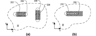
[0030] 図2は、X位置及びY位置をそれぞれ測定する基板W上に提供されたアライメントマーク202、204の例を示す。この例の各々のマークは、基板に与えられるか又はエッチングされる製品層又はその他の層に形成される一連のバーを含む。X方向のマーク202上のバーはY軸に平行で、Y方向のマーク204上のバーはX軸に平行である。アライメントセンサAS(図1に示す)は、放射スポット206、208で各々のマークを光学的にスキャンして、装置に対する基板Wの位置を測定する。スキャン運動は太い矢印で概略的に示され、スポット206又は208の漸進的位置が点線で示されている。アライメントパターン内のバーのピッチは、通常、基板上に形成される製品フィーチャのピッチよりもはるかに大きく、アライメントセンサASは、基板にパターンを付与するのに使用される露光放射よりもはるかに長い放射波長(又は普通複数の波長)を使用する。しかし、多数のバーによって繰り返しパターンの位相を正確に測定できるため、微細位置情報を得ることができる。
FIG. 2 shows an example of the alignment marks 202 and 204 provided on the substrate W for measuring the X position and the Y position, respectively. Each mark in this example includes a series of bars formed in a product layer or other layer that is applied to the substrate or etched. The bar on the
[0031] 粗及び微細マークを提供でき、したがってアライメントセンサはパターンのどの周期が所与の位置にあるか、またその周期内の正確な位置(位相)を計算できる。このために異なるピッチのマークを使用することができる。これらの技術も当業者には周知であり、本明細書では詳述しない。そのようなセンサの設計及び動作は当技術分野で周知であり、各々のリソグラフィ装置は専用に設計されたセンサを有する。本発明の説明では、アライメントセンサASはUS6961116号(den Boef)に記載の形態のアライメントシステムを備える。図2(b)は、1回のスキャンでX及びY位置が得られる同様のアライメントシステムと併用する改良されたマークを示す。マーク210は、X軸及びY軸の両方に対して45度の角度に配置されたバーを有する。その内容が参照により本明細書に組み込まれている公開特許出願US2009195768A号(Bijnen他)に記載されている技術を用いてこのX軸及びY軸方向の組合せ測定を実行できる。なお、US’768は、X−Yアライメントマークが本出願で新しく提示されるマークにやや類似した、異なるピッチの部分を有する幾つかの実施形態を開示している。しかし、図2(b)に示すより簡単なマークが商用実施形態で通常使用される形態であり、US’768の実施形態の異なるピッチ間で観察できるモアレ効果は固定し、工程性能の尺度を提供しない。 [0031] Coarse and fine marks can be provided so that the alignment sensor can calculate which period of the pattern is at a given position and the exact position (phase) within that period. For this purpose, marks with different pitches can be used. These techniques are also well known to those skilled in the art and will not be described in detail herein. The design and operation of such sensors is well known in the art, and each lithographic apparatus has a specially designed sensor. In the description of the invention, the alignment sensor AS comprises an alignment system of the form described in US6961116 (den Boef). FIG. 2 (b) shows an improved mark for use with a similar alignment system that provides X and Y positions in a single scan. The mark 210 has a bar disposed at an angle of 45 degrees with respect to both the X axis and the Y axis. This combined X-axis and Y-axis measurement can be performed using the technique described in published patent application US2009195768A (Bijnen et al.), The contents of which are incorporated herein by reference. Note that US'768 discloses several embodiments in which the XY alignment marks have portions with different pitches that are somewhat similar to the marks newly presented in this application. However, the simpler mark shown in FIG. 2 (b) is the form normally used in commercial embodiments, the moiré effect that can be observed between different pitches of the US'768 embodiment is fixed, and the scale of process performance is reduced. Do not provide.
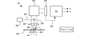
[0032] 図3は、アライメントセンサASの概略ブロック図である。照明源220は、対物レンズ224を通して基板W上に位置するマーク202などのマークに向けられる1つ又は複数の波長の放射ビーム222を提供する。図2に概略を示すように、上記のUS6961116号に基づく本発明のアライメントセンサの例では、それによってマーク202が照明される照明スポット206は、マーク自体の幅よりも直径がわずかに小さくてもよい。
FIG. 3 is a schematic block diagram of the alignment sensor AS. The
[0033] マーク202によって散乱された放射は対物レンズ224によって集められ、コリメートされて情報搬送ビーム226になる。自己参照型干渉計228は、ビーム226を処理し、センサアレイ230上に別々のビームを出力する。センサグリッド230内の個々のセンサからの強度信号232が処理ユニットPUに提供される。ブロック228内の光学処理とユニットPU内の演算処理との組合せによって、センサに対する基板上のX及びY位置の値が出力される。処理ユニットPUは図1に示す制御ユニットLACUとは別個のものであってもよく、又は設計選択及び便宜の問題として、同じ処理ハードウェアを共用していてもよい。ユニットPUが別個の場合、信号処理の一部がユニットPU内で実行され、別の部分がユニットLACU内で実行されてもよい。
The radiation scattered by the
[0034] 上記のように、図示の特定の測定は、マークの1つのピッチに対応する一定範囲内にマークの位置を固定する。これに関連して粗測定技術が使用され、正弦波のどの周期がマークされた位置を含む周期であるかが識別される。粗及び/又は微細レベルでの同じ工程を異なる周波数で繰り返して精度を高め、マークの製造材料又はマークの下の材料とは無関係にマークの検出を堅牢にすることができる。各波長を光学的に多重化及び多重分離して同時に処理できるようにし、及び/又は各波長を時分割多重化してもよい。本開示内の例は1つの波長での1回の測定のみについて述べているが、当業者であればその教示を拡張して局所区域的で堅牢な測定装置(アライメントセンサ)を提供するのに必要な変更を容易に理解できよう。 [0034] As described above, the particular measurement shown fixes the position of the mark within a certain range corresponding to one pitch of the mark. In this connection, a coarse measurement technique is used to identify which period of the sine wave is the period containing the marked position. The same process at the coarse and / or fine level can be repeated at different frequencies to increase accuracy and to make the detection of the mark robust regardless of the manufacturing material of the mark or the material under the mark. Each wavelength may be optically multiplexed and demultiplexed to allow simultaneous processing and / or each wavelength may be time division multiplexed. While the examples in this disclosure describe only one measurement at one wavelength, those skilled in the art can extend the teaching to provide a local area and robust measurement device (alignment sensor). Make the necessary changes easy to understand.
[0035] 測定工程を詳細に説明すると、図3のvWの標識を付けた矢印は、スポット206がマーク202の全長Lを横断するスキャン速度を示す。この例では、アライメントセンサASとスポット206とは実際には静止しているが、速度vWで移動するのは基板Wである。よってアライメントセンサは堅固に且つ正確に基準フレームRF(図1)に装着でき、基板Wの移動方向と逆の方向にマーク202を効率的にスキャンできる。基板は、この移動において基板テーブルWT上への装着と基板位置決めシステムPWとによって制御される。最初に説明したように、高価なリソグラフィ装置に要求される高い生産性要件では、基板上の多数の位置のアライメントマークの測定をできるだけ迅速に実行することが要求される。これは、スキャン速度vWが高速で、各々のマーク位置の取得に使用できる時間TACQがそれに応じて短いということを意味する。単純化した用語では、式TACQ=L/vWが適用される。
Describing the measurement process in detail, the arrow labeled v W in FIG. 3 indicates the scan speed at which the
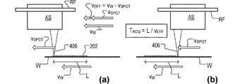
[0036] 残念なことに、取得時間が短いため、測定位置x及びyの精度は低下する。これは測定工程自体が困難であるというだけでなく、取得時間が基板テーブルWT及びその上に支持される基板Wの移動時の動的位置決めエラーを取り除くには短すぎるということにもよる。単純には振動と考えられ得るこれらの動的位置決めエラーは、当技術分野でMSDエラー(MSDは移動標準偏差を表す)と呼ばれる。これらのMSDエラーを除去するために、測定を繰り返して平均の結果を使用してもよいが、測定時間全体が増加するため、スループットを増大させるという目的にそぐわない。要するに、既知のタイプのスキャンアライメントセンサで達成可能な精度を制限する競合する要因が存在する。本明細書で開示される新規の構成では、スポット206がアライメントセンサと基準フレームに対してスキャン運動をする。したがって、動作全体を低速化することなく取得時間を延ばすことができる。この技術について以下に詳述する。
[0036] Unfortunately, the accuracy of the measurement positions x and y is reduced due to the short acquisition time. This is not only because the measurement process itself is difficult, but also because the acquisition time is too short to eliminate dynamic positioning errors when moving the substrate table WT and the substrate W supported thereon. These dynamic positioning errors, which can be considered simply as vibrations, are referred to in the art as MSD errors (MSD stands for moving standard deviation). In order to eliminate these MSD errors, the average result may be used by repeating the measurement, but the total measurement time is increased, which is not suitable for the purpose of increasing the throughput. In short, there are competing factors that limit the accuracy achievable with known types of scan alignment sensors. In the novel configuration disclosed herein, the
[0037] 図4に、好都合には上記と同じマークであるマーク202上の改良型アライメントセンサASのスキャン動作の開始(a)と終了(b)とを示す。マークの全長はここでもLで、基板Wはここでも速度vWでアライメントセンサの下を移動する。しかし、この改良動作では、照明スポット406、又はより一般的には、スキャン動作中の任意の所与の瞬間にアライメントセンサによって読み出されるマーク202上の地点が速度vSPOTで基準フレームRFに対して移動するよう制御される。このスポット速度vSPOTは基板速度vWより幾分小さい。スポット406のこの光学スキャン運動の効果は、基板速度vWとスポット速度vSPOTとの間の差分であるスキャンの有効速度vEFFが基板速度自体よりもはるかに小さいということである。したがって、取得時間TACQ=L/vEFFは、全体スキャン速度の意味するところよりも長い。これによって、マーク202上の位置測定の精度が上がり、特に全体の測定時間を増加させることなくMSDエラーを除去することができる。
FIG. 4 shows the start (a) and end (b) of the scanning operation of the improved alignment sensor AS on the
[0038] 取得時間を長くすることの効果がどれだけ大きく達成可能か又は所望されるかに限界があることは当然である。これらの限界は第1に、スキャン運動全体をカバーするのに十分な幅の視界(FOV, Field of View)を有する必要があり、また全スポット位置で一定の均一性、安定性及び/又は応答予測可能性を有する必要があるアライメントセンサ光学システムの光学特性に依存する。図5を参照しながら実際の構成について説明する。 [0038] Of course, there is a limit to how much the effect of increasing the acquisition time can be achieved or desired. First of all, these limits need to have a field of view (FOV) that is wide enough to cover the entire scan motion, and a uniform uniformity, stability and / or response at all spot locations. Depends on the optical properties of the alignment sensor optical system that need to have predictability. The actual configuration will be described with reference to FIG.
[0039] 図5は、その動作原理を図4を参照しながら上に図示し説明したスキャンスポットを実施する改良型アライメントセンサの光学システム500を示す。光学システム500は、上記の先行公開であるUS6961116号に記載のシステムの改良版である。特に本出願に関連する第1の改良は、上記のスキャン照明スポットである。第2の改良は、とりわけ精度向上のためにアライメントマークのピッチの低減を可能にさせ、また、個別のスキャトロメータ装置ではなくアライメントセンサでスキャトロメトリタイプの測定を実行できる、特定のセグメント化照明モードの使用である。上記のUS2009/195768号の開示に基づいてさらに改良を加えることができ、X及びY位置の同時測定が可能である。本説明の目的としては、位置測定は一方向のみとする。
FIG. 5 illustrates an improved alignment sensor
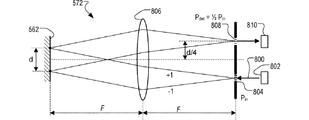
[0040] 図3の概略図との比較を容易にするために、光学システム500の幾つかの部品は図3で使用したのに類似する参照符号を付けているが、プレフィックスは「2」ではなく「5」である。したがって、光源520、照明ビーム522、対物レンズ524、情報搬送ビーム526、干渉計528及び検出器530a及び530bが示されている。これらの検出器からの信号532a及び532bは、下記の新規の特徴を適宜実施するために改良された処理ユニットPUによって処理される。幾つかの枝を有する光軸Oは、光学システム500を通り抜ける破線によって示されている。この詳細概略図に示す追加のコンポーネントは以下の通りである。照明サブシステム540では、光源520からの放射が、光ファイバ542を介してレンズ544及び546を備える光学システムに進入する地点へ送達される。各々のレンズが単一の素子で概略的に示されている場合、実際の実施形態は現実には素子のグループを含んでもよく、又は反射光学素子が使用されてもよいことは当然である。レンズ544と546との間では、ビームは平行で、対物レンズ524の瞳面Pの逆投影である平面P’を通過する。この平面には、固定式又は構成可能な照明アパーチャ548が提供され、図5に示す対称のセグメント化照明パターンなどの特定の照明モードを可能にしている。a及びbとラベル付けられた2つの直径方向に対向する象限がこのアパーチャパターン内では明るい(透明である)が、他方の2つの象限は暗い(不透明である)。このタイプのアパーチャは特許出願US2010/201963号のスキャトロメトリ装置で既知である。この改良型照明アパーチャの利点は以下にさらに説明される。固定ミラー550による回折とレンズ552によるコリメーションの後で、照明ビーム522は照明サブシステム540からビームスプリッタ554へ送達され、ビームスプリッタ554は既知の装置におけるのと同様、照明ビーム522を情報搬送ビーム526から分離する。
[0040] For ease of comparison with the schematic of FIG. 3, some parts of the
[0041] しかし、既知のアライメントセンサとは異なり、照明ビーム522と情報搬送ビーム526とは、直接対物レンズ524を通して基板Wまで固定した形で基板Wとの間を往復しない。むしろ、この改良型装置では、スキャンサブシステム560が対物レンズ524と光学システム500の残りの部分との間に介在して、照明スポット506に基板W自体のスキャン運動に加えてスキャン運動を実施させる。このスキャン運動は、図4の概略図でスポット406について示す速度vSPOTを持つ運動である。この実施形態のスキャンサブシステム560は、ビーム522及び526を小さい可変角度で偏向させる可動、具体的には傾斜ミラー562に基づいている。ミラー562は、ヒンジ点568で支持体566に接続されたアーム564上に装着されて、ある角度範囲内の所望の角度まで枢動する。ミラー562又はその支持体への機械的接触を有しない磁気アクチュエータなどのアクチュエータ570によって、ミラー562は所望の角度まで移動してスポット506をスキャン運動のための所望の位置まで移動させる。この実施形態では、アーム564とヒンジ点568は、以下に詳述する固有共振周波数を有する質量スプリング振動系を、ミラー562を用いて実施する。そのような実施形態では、アクチュエータ570は、比較的明確な周波数でのミラーの平滑な揺動を引き起こすように、適当な周波数での極めてわずかなエネルギー入力のみを提供することができる。光学測定によって傾斜角を正確にモニタする傾斜センサ572が提供される。アクチュエータ570は、傾斜センサ572からの信号も受信し、位置決めサブシステムPWによる基板テーブルWTのスキャン運動を含む通常アライメントセンサの測定動作に同期したコントローラ(ユニットPUの一部であってもよい)の制御下にある。
However, unlike the known alignment sensor, the
[0042] スキャンサブシステム560について図6〜図8を参照しながら以下に詳述する。情報搬送ビーム526の処理について説明すると、これはUS6961116号の既知のアライメントセンサと同様に干渉計528内に進入する。干渉計528は、簡略化された2次元構成で示されているが、実際には上記先行特許に記載するようにプリズムとその他の素子の3次元構成を備える。同様に、干渉計の一部である偏光素子はここでは図を見やすくするために省略されている。自己参照型干渉計528の機能は、既知の例と同様、情報搬送ビーム526を受光し、それを2つの等しい部分に分割し、それらの部分を互いに180度回転させ、それらの部分を再度組み合わせて出射ビーム582を形成する。ビーム582は、検出サブシステム580へ誘導される。レンズ584及び586は、固定偏向ミラー588と共に、このビームを偏光ビームスプリッタ590を介して検出器530a及び530bへ送達する。
The
[0043] ビームスプリッタ590は、互いに逆相の2つの干渉パターンを生成する。したがって、干渉計528が検出器530a上の一地点で破壊的な干渉を生成すると、検出器530bの対応する地点に建設的干渉が同時に生成される。2つの検出器から信号を減算することで、共通モード強度雑音の影響を低減し、アライメントセンサから全体としてより高精度の出力を得ることができる。
[0043] The
[0044] 図3の既知のアライメントセンサでは検出器230は基板Wの平面に対応する像平面に配置される一方、改良型光学システム500内の検出器530a及び530bは対物レンズ524の瞳面Pと共役の平面P”内に配置されている。この例の各々の検出器530a及び530bは、画像センサ、例えばCCDカメラセンサである。代替実施形態では、画像センサの代わりに個別の地点検出器を配備してもよい。いずれにせよ、平面P”の放射電磁界は基板の像ではなく、照明アパーチャ548と共役のマーク202の回折スペクトルである。このタイプの検出システムでは、マーク202の位置情報を得るのに必要なアライメント信号は依然として取得可能であるが、さらに、検出器530a及び530bによって検出される瞳面の像を用いて基板W上のマーク又はその他の特徴の追加の特徴を解析してスキャトロメトリを実行できる。例えば、アライメント及び/又はオーバレイターゲットの対称性を解析でき、それによって例えばデバイス層間のオーバレイエラーの測定が容易になる。別個の装置ではなくアライメントセンサを用いてターゲットの対称性を測定することの利益は、アライメントセンサとオーバレイ測定装置との間の位置決めエラーが解消されるということである。
In the known alignment sensor of FIG. 3, the
[0045] アパーチャ548によって提供される照明パターンが図5でa及びbとラベルされた明るい象限を有する一方で、アライメントマーク202のラインによる所与の方向の回折から発生する回折パターンが548’のパターンによって表されている。このパターンでは、a0及びb0とラベル付けられたゼロ次反射に加えて、a−1、a+1、b−1及びb+1とラベル付けられた可視1次回折信号が存在する。照明アパーチャのその他の象限は暗いため、またより一般的には照明パターンが180°回転対称を有するため、回折次数a−1及びb+1は「フリー」(“free”)状態である。これは、それらの次数がゼロ次数又は照明アパーチャの他の部分からの高次信号と重ならないということを意味する。セグメント化された照明パターンのこの特性を活用して、従来の円形対称照明アパーチャを使用した場合に結像可能な最小ピッチの半分のピッチを有する回折格子(アライメントマーク)から明瞭な1次信号を得ることができる。この回折パターン548’とそれをスキャトロメトリに活用できる方法が、既知の出願US2010/201963号に記載されている。アライメントセンサ光学システム500の干渉計528では、図5に示され548”とラベル付けられた回折パターン548’の回転コピーも形成され、パターン548’と混合される。これらのパターンは、アライメントマーク202のスキャン中に互いに干渉して、位置信号を提供する。
[0045] While the illumination pattern provided by
[0046] スキャンサブシステム560に関して、ここに示す特定の形態のスキャンサブシステムは、以下に説明する幾つかの有利な特徴を有する。
[0046] With respect to the
[0047] 図5及び図6に示すように、傾斜ミラー562の取付けのジオメトリは、枢動ポイント568が対物レンズ524の瞳面Pと同じ平面内に位置する。ミラー562の前後の傾斜は、ビーム522が対物レンズ524に進入するビームの方向の偏向を引き起こし、その結果、所望の速度vSPOTでのスポット506の前後のスキャン運動が実行される。より具体的には、ミラー562はミラーの本体内にはなく、ミラー562の平面と対物レンズ524の瞳面Pとが交差する線内の、又はその付近の軸を中心に傾斜するように装着される。背景として、逆投影された平面P’の照明アパーチャが移動することなく、照明スポット506を形成する光線の方向が移動してスキャン速度vSPOTを実施することが望ましい。例えば、傾斜ミラーが一般にそうであるように、ミラー562がその中心軸を中心に傾斜した場合、照明源は逆投影された瞳面P’内を前後に移動し、基板上の照明スポットの平均入射角が変動することになるであろう。
As shown in FIGS. 5 and 6, the mounting geometry of the
[0048] 基板上の正常な入射角を維持することでアライメントの精度が向上する。これを達成するための従来の解決策は、光学システムの共役瞳面内に傾斜ミラーを配置して、照明スポット又は視界のスキャン運動を達成することであろう。しかし、ここに示すアライメントセンサなどの実際の装置では、市販の対物レンズ524は、通常、小型で自立型のサブアセンブリ内に収容され、傾斜ミラー又はその他の可動素子を介在させるスペースは瞳面P内には存在しない。瞳面内に傾斜ミラーを含むようにカスタム設計アセンブリを作ることができ、又は追加の光学素子を提供して光学経路内の混雑していない地点に共役瞳面を生成できるが、アセンブリのコストは以前よりもはるかに高くなり、精度が低下する可能性がある。
[0048] Alignment accuracy is improved by maintaining a normal incident angle on the substrate. A conventional solution to achieve this would be to place a tilting mirror in the conjugate pupil plane of the optical system to achieve a scanning motion of the illumination spot or field of view. However, in an actual apparatus such as the alignment sensor shown here, the commercially available
[0049] 図6を参照すると、光線522及びミラー表面562のジオメトリが、第1にミラーの中央又は中間位置(562(0)とラベルされている)に関して、次に対物レンズ524の瞳面Pと同じ平面にある枢動ポイント568を中心に回転するミラーが入射波522から角度θだけ離れて傾いた偏向位置562(θ)に関して、示されている。この例でのミラーの静止位置は、瞳面と入射光線の方向に対して45°である。角移動θが一方向に示されている一方、同じ運動を逆方向に(光線522の光源のより近くに)ミラーに付与してもよい。これは、ミラー562が角度範囲θだけ前後に揺れ動いているからである。破線の円内の拡大図は、光線522が静止位置及び偏向位置のミラー562によって反射する領域内のジオメトリを示す。実際の実施形態でミラーが偏向する角度範囲θは数ミリラド又は数十ミリラド程度であってもよく、ミラーの傾斜によって引き起こされる光学経路の変化を計算するときに「微小角近似」(“small angle approximation”)を適用できる。図に示すように、瞳面P及び入射光線522の経路は距離Dだけ離間しているが、ミラー562のデフォルト位置は光線522を直角に偏向させる45°である。ミラーが角度θ傾斜するとき、偏向した光線522’は角度2θ傾斜するが、ミラーとの交差点も距離2θD左に移動する。したがって、偏向した光線522が瞳面Pと交差する地点600は、少なくともほぼ、ミラーの傾斜角θから独立している。このことから、照明アパーチャ548の有効位置は変化しないが、光線の方向、したがって照明スポット506の位置は角度θに応じて前後に移動する。(線速度vSPOTは対物レンズ524の倍率掛ける角度2θに関連する。)
[0049] Referring to FIG. 6, the geometry of the
[0050] 図7は、例示的実施形態での時間tにわたるミラー562の傾斜角θの変化を表す正弦曲線700を示す。トレース700は、上述したように、傾斜角562とその取付物が共振振動子として駆動されるため、通常、正弦形状を持つ。言い換えれば、ミラーは単振動(simple harmonic motion)で傾斜する。ミラーの揺動の期間はTOSCとラベル付けられ、揺動の角度θで表す振幅はθOSCである。この駆動モードの利点は、最小のエネルギー入力を必要とし、したがって、アクチュエータとミラー機構内の最小の熱放散を必要とするということである。この駆動モードの欠点は、所望の速度と方向のスキャン運動が、特定の間隔で、且つ運動の限られた直線性しか伴わずに実行されるということである。しかし、このミラーの揺動を基板Wにわたる一連のアライメントマーク202のスキャン中に基板が移動する方法と同期化させる処理を含む測定工程の慎重な設計によって、アライメントマーク位置の測定を図7にてM1、M2、M3とラベルされた期間実行できるように、ミラー揺動の周期を選択できる。これらは、ミラーの運動、及びよってアライメントマーク202に沿ったスポット506の運動が比較的直線的で予測可能であるトレース700の部分である。スキャン測定が実行される角度範囲はθMとラベルされ、スポット506のスキャン運動を用いて1回又は複数回の測定を実行できる時間ウィンドウはTMとラベルされている。装置は、この期間中に1つのアライメントマークを測定する動作に限定されず、基板W上のその位置と基板テーブルWT上の基板の運動とに応じて、幾つかのマークを測定できる。図8は、傾斜センサ572の構造と動作原理を概略的に示す。図5に関連して述べたように、傾斜センサは、常時、傾斜562の正確な測定値を提供するために提供される。この測定値は、ユニットPU又はその他のコントローラによって、スキャン運動、アクチュエータ570による駆動、測定期間M1、M2、M3などにおける非直線性の補正及び適宜その他の測定を必要に応じて制御し同期化するために、用いられることができる。この例では、傾斜センサ572は、周知の位相格子検出器に基づいている。放射源802からの放射ビーム800は、ピッチPINを有する第1の位相格子によって回折させられる。図で+1及び−1とラベル付けられた1次光線だけが任意の強度で伝送されるように、位相格子を使用できる。これらの光線は、図示のように発散している。傾斜センサ光学システム806は光線が平行になるようにコリメートし、したがって、+1次及び−1次光線は距離dだけ離間した別個の地点でミラー562の表面に入射する。(例えば、この距離dは数ミリメートル程度であってもよい。)回折した光線は光学システム806を通して反射し、検出格子808上に合焦する。検出格子808は、入力格子804のピッチの半分のピッチPdetを有する。ミラー562内の傾斜角は、+1及び−1回折次数について異なる経路長を生じさせ、これは、それらが格子808で再度結合されるときにそれらの位相に影響する。検出器810は、検出格子808を通過する回折放射を受光する。ミラーが一方向、次に他の方向に傾斜すると、810で検出される放射強度の急速な変動は、傾斜角の微小な変動のカウントを可能ならしめる。これらの変動をカウントする(フリンジカウント)ことで、比較的広範囲の傾斜角にわたって傾斜の極めて高い解像度の測定値を得ることができる。傾斜角の絶対的知識を得るために、幾つかの異なる格子システム804、808及び検出器810をピッチを変えて並列に提供することができる。この曖昧性解消方法は当業者には周知であり、詳細の説明は割愛する。
[0050] FIG. 7 shows a
アライメントセンサの変形形態
[0051] 例示的実施形態の検出器530a及び530bはその領域にわたってピクセルを有する画像センサとして記述されているが、検出器が瞳像平面P”の一定の地点にだけ提供される代替実施形態も可能である。特に、1次回折照明が予想される周辺位置に数個の検出器を配置することでアライメント信号を入手できる。瞳像の周辺全体に一組の検出器を離間させることができ、マーク202がX方向かY方向か、又は図2(b)に示すタイプのX−Yマークかに従って、位置測定値を生成する処理を実行するために適当な検出器からの信号を選択することができる。
Variation of alignment sensor
[0051] Although the
[0052] 当業者であれば、本発明の範囲を逸脱することなく上記の各実施形態の多数の修正及び変更を容易に思い付くであろう。上記のように、例えば、図示のアライメントセンサを図2(b)のマークと併用するように構成させて、X及びY方向の位置情報を同時に入手することができる。そのような実施形態でセグメント化照明アパーチャ548を使用したい場合、マーク210(図2(b))の格子線が45°に配置されているのと同様に、明るいセグメントa及びbがX及びY軸の両方に対して45°の角度をなすように照明アパーチャ548を回転させる必要がある。
[0052] Persons skilled in the art will readily be able to conceive numerous modifications and changes to each of the above embodiments without departing from the scope of the present invention. As described above, for example, the illustrated alignment sensor can be configured to be used in combination with the mark of FIG. 2B, and position information in the X and Y directions can be obtained simultaneously. If it is desired to use the
[0053] この簡単な例では、揺動ミラー562はスポットを一方向にしか移動させず、マークの一方向だけが低減された有効速度でスキャンできる。2次元スキャンを所望する場合、直交する枢動軸を備えた2つの別々のミラーか、又は2つの直交枢動軸の周囲で傾斜可能な1つのミラーを使用できる。当業者であれば、いずれかの方法でこの例を2次元にまで拡張できる。
[0053] In this simple example, the
[0054] 冒頭部分などで述べたように、スキャン照明スポット406、506などを備えたアライメントセンサの文脈で開示されたある特定の特徴を他の用途で独立して使用できる。図5の実施形態の特徴である共役瞳面内の検出と組み合わせたセグメント化アパーチャを、スキャンサブシステム560を用いずに、アライメントセンサで使用してもよい。上述したように、そのようなアパーチャの使用によって、アライメントマーク内でより高密度の格子線を使用でき、位置精度を高め、及び/又はマークが必要とする基板領域を低減する可能性が生まれる。
[0054] As mentioned in the opening part and the like, certain features disclosed in the context of an alignment sensor with scan illumination spots 406, 506, etc. can be used independently in other applications. The segmented aperture combined with detection in the conjugate pupil plane that is a feature of the embodiment of FIG. 5 may be used in the alignment sensor without the
[0055] アライメントセンサを制御する処理ユニットPUは、検出した信号を処理し、これらの信号からリソグラフィパターニング工程を制御する際に使用するのに好適な位置測定値を計算し、詳述はしないがある種のコンピュータアセンブリを一般に含むことを理解されたい。コンピュータアセンブリは装置外部の専用コンピュータであってもよく、アライメントセンサ専用の1つ又は複数の処理ユニットであってもよく、又は、リソグラフィ装置全体を制御する中央制御ユニットLACUであってもよい。コンピュータアセンブリは、コンピュータ実行可能コードを含むコンピュータプログラムプロダクトを読み込むように構成されていてもよい。これによって、コンピュータプログラムプロダクトがダウンロードされると、コンピュータアセンブリはリソグラフィ装置とアライメントセンサASの上記併用を制御することができる。 [0055] The processing unit PU controlling the alignment sensor processes the detected signals and calculates suitable position measurements from these signals for use in controlling the lithographic patterning process, although not detailed. It should be understood that some sort of computer assembly is generally included. The computer assembly may be a dedicated computer external to the apparatus, may be one or more processing units dedicated to the alignment sensor, or may be a central control unit LACU that controls the entire lithographic apparatus. The computer assembly may be configured to load a computer program product that includes computer executable code. Thereby, when the computer program product is downloaded, the computer assembly can control the combined use of the lithographic apparatus and the alignment sensor AS.
[0056] 本文ではICの製造におけるリソグラフィ装置の使用に特に言及しているが、本明細書で説明するリソグラフィ装置には他の用途もあることを理解されたい。例えば、これは、集積光学システム、磁気ドメインメモリ用誘導及び検出パターン、フラットパネルディスプレイ、液晶ディスプレイ(LCD)、薄膜磁気ヘッドなどの製造である。こうした代替的な用途に照らして、本明細書で「ウェーハ」又は「ダイ」という用語を使用している場合、それぞれ、「基板」又は「ターゲット部分」という、より一般的な用語と同義と見なしてよいことが、当業者には認識される。本明細書に述べている基板は、露光前又は露光後に、例えばトラック(通常はレジストの層を基板に塗布し、露光したレジストを現像するツール)、メトロロジーツール及び/又はインスペクションツールで処理することができる。適宜、本明細書の開示は、以上及びその他の基板処理ツールに適用することができる。さらに基板は、例えば多層ICを生成するために、複数回処理することができ、したがって本明細書で使用する基板という用語は、既に複数の処理済み層を含む基板も指すことができる。 [0056] Although the text specifically refers to the use of lithographic apparatus in the manufacture of ICs, it should be understood that the lithographic apparatus described herein has other uses. For example, this is the manufacture of integrated optical systems, guidance and detection patterns for magnetic domain memories, flat panel displays, liquid crystal displays (LCDs), thin film magnetic heads, and the like. In light of these alternative applications, the use of the terms “wafer” or “die” herein are considered synonymous with the more general terms “substrate” or “target portion”, respectively. Those skilled in the art will recognize that this may be the case. The substrates described herein may be processed before or after exposure, for example, with a track (usually a tool that applies a layer of resist to the substrate and develops the exposed resist), metrology tools, and / or inspection tools. be able to. Where appropriate, the disclosure herein may be applied to these and other substrate processing tools. In addition, the substrate can be processed multiple times, for example to produce a multi-layer IC, so the term substrate as used herein can also refer to a substrate that already contains multiple processed layers.
用途例:共焦顕微鏡
[0057] アライメントセンサは、ミラーとミラーが使用される光学システムの瞳面と同じ平面に位置するように枢動軸が変位される傾斜ミラーの用途例である。この構成は、基板上への平均入射角を変更することなく照明スポットを基板平面内で偏向させる特殊な能力を有する。アライメントセンサ以外の用途にこの原理を適用でき、共焦顕微鏡は別の例である。
Application example: Confocal microscope
[0057] An alignment sensor is an application example of a tilt mirror in which the pivot axis is displaced so that the mirror and the pupil plane of the optical system in which the mirror is used are located. This configuration has the special ability to deflect the illumination spot in the substrate plane without changing the average angle of incidence on the substrate. This principle can be applied to applications other than alignment sensors, and a confocal microscope is another example.
[0058] 図9に、傾斜ミラーの用途を共焦顕微鏡1500の文脈で示す。システムの多数の部品が、少なくとも原則として上記のアライメントセンサの例に共通であり、対物レンズ1524などの部品は図5の対応する部品524と同じであるがプレフィックス「1」を付加した数字になっている。幾つかの主要な差異を以下に説明する。図示の共焦顕微鏡では、照明ビーム1522が図の上部からビームスプリッタ1554に進入する。一方、情報搬送ビーム1526は、右手に向かってビームスプリッタ1554から抜ける。この配置が実際の実施態様であり、動作原理を変更していないことは当然である。情報搬送ビーム1526はまず狭いピンホール1580上に合焦し、ピンホール1580は次に検出器1582上に結像され、検出器1582はピンホールを通過する放射の強度を記録する。共焦顕微鏡の原理から周知のように、ピンホール1580の機能は、照明がそこから検出器1582に到達する照明スポット1506内の位置と深さとの両方を選択することである。したがって、検出された放射の強度は、特定の位置でのターゲット構造1202の組成と対物レンズ1524の下の深さとに依存する。2次元のスキャン運動が実施され、検出器1582によって検出された時間変動強度信号を処理ユニット1584内で処理してターゲット1202の2次元像を得ることができる。図では、ディスプレイ1586は、結果として得られた情報が与えられて、所望の深さでのターゲット1202の特徴を極めて高い解像度で示す画像1588を提供する。
FIG. 9 illustrates the use of tilt mirrors in the context of a
[0059] 図示の例では、上記の図3の揺動ミラーとまさしく同様に装着され、駆動されモニタされる揺動ミラー1562によって、少なくとも1つの方向でのスポットのスキャンが実行される。共焦顕微鏡の動作では典型的に、一方向、例えばX軸方向のスキャンがスポット1506の何らかの光学スキャンによって実施される一方、Y方向のスキャンが対物レンズ1524の下のターゲット1202の遅い進行によって実施される。可動ミラーによる2次元スキャンを所望する場合、直交する枢動軸を備えた2つの別々のミラーか、又は2つの直交枢動軸の周囲で傾斜可能な1つのミラーを使用できる。当業者であれば、いずれかの方法でこの例を2次元にまで拡張できる。
In the illustrated example, spot scanning in at least one direction is performed by a
[0060] 実施制御及び共焦顕微鏡内の信号処理のその他の特徴は既知の例から構成できるため、ここでは詳述する必要はない。 [0060] Implementation control and other features of signal processing in the confocal microscope can be constructed from known examples and need not be described in detail here.
追加の変形形態
[0061] 上記の例では、揺動ミラーは約90°の角度で光学経路を方向転換させ、対物レンズ524又は1524の瞳面に対して45°の角度に装着される。ミラー平面と対物レンズ524/1524の瞳面Pとの交点にミラー562/1562の枢動軸を配置するという同じ原理を45°以外の角度に拡張することができる。
Additional variants
In the above example, the oscillating mirror turns the optical path at an angle of about 90 ° and is mounted at an angle of 45 ° with respect to the pupil plane of the
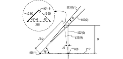
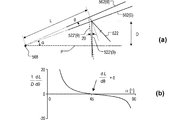
図10(a)は、図6の構成と同様であるが角度45°を一般的な角度αに変更した一般化された構成を示す。枢動軸568から照明光線522の反射地点までのミラーに沿った長さにラベルLが付けられ、Lはα=45°のときの図6の例における2の平方根のD倍の距離に等しかった。この一般化された例における様々な長さと角度との関係は、距離L、距離D、並びに角度α(静止位置)及び揺動によるθ(偏差)に関する以下の式によって表される。
![]()
![]()
![]()

![]()
![]()
![]()
[0062] 式(1)は、偏差θが安息角αよりもはるかに小さい場合に式(2)で近似できる正確な長さLの公式である。スキャン機構の設計のための最良の角度αを決定するために、式(3)はθで表した長さLの導関数を提示する。式(4)は、θがゼロのときのθに関するLの導関数の特殊な例を提示する。 [0062] Equation (1) is an exact length L formula that can be approximated by Equation (2) when the deviation θ is much smaller than the angle of repose α. In order to determine the best angle α for the design of the scanning mechanism, equation (3) presents a derivative of length L expressed in θ. Equation (4) presents a special example of the derivative of L with respect to θ when θ is zero.
図10(b)は、安息角αの様々な値について距離Dに関して正規化した式(4)の描画である。図から分かるように、このグラフはαが値45°を有する値0を備えた変曲点を有する。これから、α=45°の場合、揺動θに対する距離Lの感度が他のいかなる角度αよりも広い範囲のθにわたって最小化されると推定する。したがって、照明源の見かけ上の位置の不変性は図6に関連して提示された解析での微小角近似に依存するため、安息角α=45°は角度θの使用可能な範囲にわたって上記近似が実質的に確実に真であるようにする上で最適である。にもかかわらず、特定の配置上の制約を考慮するために45°以外の角度を使用することは興味深い。わずか数ミリラド又は数十ミリラドの揺動で本明細書に記載する用途には十分であることに留意されたい。
FIG. 10B is a drawing of Expression (4) normalized with respect to the distance D for various values of the angle of repose α. As can be seen, this graph has an inflection point with a
[0063] 光リソグラフィの分野での本発明の実施形態の使用に特に言及してきたが、本発明は文脈によってはその他の分野、例えばインプリントリソグラフィでも使用することができ、光リソグラフィに限定されないことを理解されたい。インプリントリソグラフィでは、パターニングデバイス内のトポグラフィが基板上に作成されたパターンを画定する。パターニングデバイスのトポグラフィは基板に供給されたレジスト層内に刻印され、電磁放射、熱、圧力又はそれらの組合せを印加することでレジストは硬化する。パターニングデバイスはレジストから取り除かれ、レジストが硬化すると、内部にパターンが残される。共焦顕微鏡検査法を適用してリソグラフィ工程で使用される、又は製造される物品を検査でき、また範囲のその他の検査作業に適用できる。 [0063] Although specific reference has been made to the use of embodiments of the present invention in the field of optical lithography, the present invention can be used in other fields, such as imprint lithography, depending on context, and is not limited to optical lithography. I want you to understand. In imprint lithography, the topography in the patterning device defines a pattern created on the substrate. The topography of the patterning device is imprinted in a resist layer applied to the substrate, and the resist is cured by applying electromagnetic radiation, heat, pressure, or a combination thereof. The patterning device is removed from the resist, leaving a pattern in it when the resist is cured. Confocal microscopy can be applied to inspect articles used or manufactured in a lithographic process and can be applied to a range of other inspection operations.
[0064] 本明細書で使用する「放射」及び「ビーム」という用語は、イオンビーム又は電子ビームなどの粒子ビームのみならず、紫外線(UV)放射(例えば、365nm、355nm、248nm、193nm、157nm若しくは126nm、又はこれら辺りの波長を有する)及び極端紫外線(EUV)放射(例えば、5nm〜20nmの範囲の波長を有する)を含むあらゆるタイプの電磁放射を網羅する。 [0064] As used herein, the terms "radiation" and "beam" include not only particle beams such as ion beams or electron beams, but also ultraviolet (UV) radiation (eg, 365 nm, 355 nm, 248 nm, 193 nm, 157 nm). Or any type of electromagnetic radiation including extreme ultraviolet (EUV) radiation (e.g. having a wavelength in the range of 5 nm to 20 nm).
[0065] 「レンズ」という用語は、状況が許せば、屈折型、反射型、磁気型、電磁型及び静電型光学コンポーネントを含む様々なタイプの光学コンポーネントのいずれか一つ、又はその組合せを指すことができる。 [0065] The term "lens" refers to any one or a combination of various types of optical components, including refractive, reflective, magnetic, electromagnetic and electrostatic optical components, as the situation allows. Can point.
[0066] 以上、本発明の特定の実施形態を説明したが、説明とは異なる方法でも本発明を実践できることが理解される。例えば、本発明は、上記で開示したような方法を述べる機械読み取り式命令の1つ又は複数のシーケンスを含むコンピュータプログラム、又はこのようなコンピュータプログラムを内部に記憶したデータ記憶媒体(例えば半導体メモリ、磁気又は光ディスク)の形態をとることができる。 [0066] While specific embodiments of the invention have been described above, it will be appreciated that the invention may be practiced otherwise than as described. For example, the present invention provides a computer program that includes one or more sequences of machine-readable instructions that describe a method as disclosed above, or a data storage medium (eg, semiconductor memory, etc.) that stores such a computer program. Magnetic or optical disk).
[0067] 上記の説明は例示的であり、限定的ではない。それ故、添付の特許請求の範囲から逸脱することなく、記載されたような本発明を変更できることが当業者には明白である。 [0067] The descriptions above are intended to be illustrative, not limiting. Thus, it will be apparent to one skilled in the art that modifications may be made to the invention as described without departing from the scope of the claims set out below.
Claims (15)
前記光学システムと前記対物レンズとの間に配置され、前記対物レンズを前記放射線が通過する際に前記放射線の方向を変えるように傾斜するミラーを備える、少なくとも1つの可動素子をさらに備え、
前記ミラーが、前記対物レンズの瞳面と前記ミラーの平面との間の交点にほぼ沿った軸を中心に傾斜するように強制される、光学装置。 An optical device comprising an objective lens for transmitting radiation between the optical system of the device and an object,
At least one movable element comprising a mirror disposed between the optical system and the objective lens and tilted to change the direction of the radiation as the radiation passes through the objective lens;
An optical device in which the mirror is forced to tilt about an axis substantially along the intersection between the pupil plane of the objective lens and the plane of the mirror.
前記マークを前記対物レンズを介して放射スポットで照明する照明サブシステムと、前記マークによって回折した放射を前記対物レンズを介して検出する検出サブシステムとを備える前記光学システムと、
前記基板と測定光学システムの動きを互いに対して第1の速度で制御して、前記マークを前記放射スポットでスキャンしながら、前記回折放射を表す信号を検出し処理して前記測定光学システムの基準フレームに対する前記マークの位置を計算する第1の位置決めサブシステムと、
前記放射スポットを前記測定光学システムの前記基準フレームに対して第2の速度で移動させるために前記第1の位置決めサブシステムと同期して動作可能な前記可動光学素子とを備え、
前記第1及び第2の速度が、前記信号が検出されている間に前記第1の速度より低い第3の速度で前記スポットが前記マークをスキャンする関係にある、装置。 The apparatus according to any one of claims 1 to 3, wherein the position of the mark on the substrate is measured.
The optical system comprising: an illumination subsystem that illuminates the mark with a radiation spot through the objective lens; and a detection subsystem that detects radiation diffracted by the mark through the objective lens;
Control of the movement of the substrate and measurement optical system at a first speed relative to each other, detecting and processing a signal representative of the diffracted radiation while scanning the mark with the radiation spot to provide a reference for the measurement optical system A first positioning subsystem for calculating the position of the mark relative to the frame;
The movable optical element operable to synchronize with the first positioning subsystem to move the radiation spot at a second speed relative to the reference frame of the measurement optical system;
The apparatus wherein the first and second velocities are in a relationship where the spot scans the mark at a third speed that is lower than the first speed while the signal is detected.
オブジェクトを前記対物レンズを介して放射スポットで照明する照明サブシステムと、前記オブジェクトによって前記放射スポットにおける特定の地点で反射された放射を前記対物レンズを介して検出する検出サブシステムとを備える前記光学システムと、
前記放射スポットと前記特定の地点とを少なくとも第1のスキャン方向にスキャンして、前記オブジェクトにわたって地点の線から検出された放射強度を記録するように動作可能な前記可動光学素子と
を備える装置。 An apparatus according to claim 1, 2 or 3, comprising a confocal microscope for inspection of objects,
The optical comprising: an illumination subsystem that illuminates an object with a radiation spot through the objective lens; and a detection subsystem that detects radiation reflected by the object at a specific point in the radiation spot through the objective lens System,
An apparatus comprising: the movable optical element operable to scan the radiation spot and the specific point in at least a first scan direction and record a radiation intensity detected from a line of points across the object.
基板を保持する基板テーブルと、前記リソグラフィ装置の基準フレームに対する前記基板上のマークの位置を測定するアライメントセンサとを備え、
前記アライメントセンサが、請求項4から7のいずれかに記載の測定装置を備え、
前記リソグラフィ装置が、前記測定装置を用いて測定される前記基板上のマークの位置を基準にして前記基板上へのパターンの転写を制御するように構成された、リソグラフィ装置。 A lithographic apparatus configured to transfer a pattern from a patterning device onto a substrate,
A substrate table for holding the substrate; and an alignment sensor for measuring a position of the mark on the substrate with respect to a reference frame of the lithographic apparatus,
The alignment sensor comprises the measuring device according to any one of claims 4 to 7,
A lithographic apparatus, wherein the lithographic apparatus is configured to control transfer of a pattern onto the substrate relative to a position of a mark on the substrate measured using the measuring device.
前記対物レンズの前に前記放射線の経路内にミラーを配置すること、及び
前記放射線が対物レンズを通過する際に前記放射線の方向を変更するようにミラーを傾斜させて、それにより前記ミラーの傾斜角に従って前記放射線を前記オブジェクトの異なる部分に入射させることを含み、
前記ミラーが、前記対物レンズの瞳面と前記ミラーの平面との間の交点にほぼ沿った軸を中心に傾斜するように強制される、方法。 A method of scanning an object with radiation through an objective lens,
Placing a mirror in the path of the radiation in front of the objective lens, and tilting the mirror to change the direction of the radiation as the radiation passes through the objective lens, thereby tilting the mirror Injecting the radiation into different parts of the object according to angles;
The method wherein the mirror is forced to tilt about an axis substantially along the intersection between the pupil plane of the objective lens and the plane of the mirror.
Applications Claiming Priority (4)
| Application Number | Priority Date | Filing Date | Title |
|---|---|---|---|
| US201161444373P | 2011-02-18 | 2011-02-18 | |
| US61/444,373 | 2011-02-18 | ||
| US201161468208P | 2011-03-28 | 2011-03-28 | |
| US61/468,208 | 2011-03-28 |
Publications (2)
| Publication Number | Publication Date |
|---|---|
| JP2012175103A true JP2012175103A (en) | 2012-09-10 |
| JP5466721B2 JP5466721B2 (en) | 2014-04-09 |
Family
ID=46652455
Family Applications (2)
| Application Number | Title | Priority Date | Filing Date |
|---|---|---|---|
| JP2012027626A Active JP5438148B2 (en) | 2011-02-18 | 2012-02-10 | Measuring method, measuring apparatus, and lithographic apparatus |
| JP2012027606A Active JP5466721B2 (en) | 2011-02-18 | 2012-02-10 | Optical apparatus, scanning method, lithographic apparatus, and device manufacturing method |
Family Applications Before (1)
| Application Number | Title | Priority Date | Filing Date |
|---|---|---|---|
| JP2012027626A Active JP5438148B2 (en) | 2011-02-18 | 2012-02-10 | Measuring method, measuring apparatus, and lithographic apparatus |
Country Status (6)
| Country | Link |
|---|---|
| US (2) | US9303978B2 (en) |
| JP (2) | JP5438148B2 (en) |
| KR (2) | KR101386057B1 (en) |
| CN (2) | CN102645847A (en) |
| NL (2) | NL2008110A (en) |
| TW (2) | TWI459153B (en) |
Cited By (8)
| Publication number | Priority date | Publication date | Assignee | Title |
|---|---|---|---|---|
| JP2012191177A (en) * | 2011-02-18 | 2012-10-04 | Asml Netherlands Bv | Measuring method, measuring apparatus, lithographic apparatus and device manufacturing method |
| WO2015098282A1 (en) * | 2013-12-26 | 2015-07-02 | 東京エレクトロン株式会社 | Substrate processing system, substrate transport method, and computer storage medium |
| WO2016104511A1 (en) * | 2014-12-24 | 2016-06-30 | 株式会社ニコン | Measurement device and measurement method, exposure device and exposure method, and device production method |
| WO2016125790A1 (en) * | 2015-02-05 | 2016-08-11 | 株式会社ニコン | Measurement device and measurement method, exposure device and exposure method, and device manufacturing method |
| JPWO2016104513A1 (en) * | 2014-12-24 | 2017-11-24 | 株式会社ニコン | MOBILE BODY CONTROL METHOD, EXPOSURE METHOD, DEVICE MANUFACTURING METHOD, MOBILE BODY DEVICE, AND EXPOSURE APPARATUS |
| JP2018527630A (en) * | 2015-08-28 | 2018-09-20 | エーエスエムエル ネザーランズ ビー.ブイ. | Lithographic apparatus, lithography alignment method, and data processing system |
| JP2019504364A (en) * | 2016-01-26 | 2019-02-14 | シャンハイ マイクロ エレクトロニクス イクイプメント(グループ)カンパニー リミティド | Scan reflective mirror monitoring system and method, focus leveling system |
| JP2021535419A (en) * | 2018-08-29 | 2021-12-16 | エーエスエムエル ホールディング エヌ.ブイ. | Compact alignment sensor arrangement |
Families Citing this family (43)
| Publication number | Priority date | Publication date | Assignee | Title |
|---|---|---|---|---|
| EP2458441B1 (en) * | 2010-11-30 | 2022-01-19 | ASML Netherlands BV | Measuring method, apparatus and substrate |
| NL2010259A (en) | 2012-04-12 | 2013-10-16 | Asml Holding Nv | Position measuring method, position measuring apparatus, lithographic apparatus and device manufacturing method, optical element. |
| NL2010717A (en) * | 2012-05-21 | 2013-11-25 | Asml Netherlands Bv | Determining a structural parameter and correcting an asymmetry property. |
| US9606442B2 (en) | 2012-07-30 | 2017-03-28 | Asml Netherlands B.V. | Position measuring apparatus, position measuring method, lithographic apparatus and device manufacturing method |
| NL2011181A (en) | 2012-08-16 | 2014-02-18 | Asml Netherlands Bv | Method and apparatus for measuring asymmetry of a microstructure, position measuring method, position measuring apparatus, lithographic apparatus and device manufacturing method. |
| NL2011477A (en) * | 2012-10-10 | 2014-04-14 | Asml Netherlands Bv | Mark position measuring apparatus and method, lithographic apparatus and device manufacturing method. |
| WO2014062972A1 (en) * | 2012-10-18 | 2014-04-24 | Kla-Tencor Corporation | Symmetric target design in scatterometry overlay metrology |
| CN103777476B (en) * | 2012-10-19 | 2016-01-27 | 上海微电子装备有限公司 | A kind of off-axis alignment system and alignment methods |
| JP6367209B2 (en) * | 2012-10-26 | 2018-08-01 | マッパー・リソグラフィー・アイピー・ビー.ブイ. | Measuring the position of a substrate in a lithography system |
| NL2011726A (en) * | 2012-11-05 | 2014-05-08 | Asml Netherlands Bv | Method and apparatus for measuring asymmetry of a microstructure, position measuring method, position measuring apparatus, lithographic apparatus and device manufacturing method. |
| US8941085B2 (en) | 2013-03-14 | 2015-01-27 | Taiwan Semiconductor Manufacturing Company, Ltd. | Electron beam lithography systems and methods including time division multiplex loading |
| US9030661B1 (en) * | 2013-03-15 | 2015-05-12 | Kla-Tencor Corporation | Alignment measurement system |
| US9733572B2 (en) | 2013-03-20 | 2017-08-15 | Asml Netherlands B.V. | Method and apparatus for measuring asymmetry of a microstructure, position measuring method, position measuring apparatus, lithographic apparatus and device manufacturing method |
| US9696264B2 (en) | 2013-04-03 | 2017-07-04 | Kla-Tencor Corporation | Apparatus and methods for determining defect depths in vertical stack memory |
| WO2014193854A1 (en) * | 2013-05-27 | 2014-12-04 | Kla-Tencor Corporation | Scatterometry overlay metrology targets and methods |
| US9740108B2 (en) * | 2013-05-27 | 2017-08-22 | Kla-Tencor Corporation | Scatterometry overlay metrology targets and methods |
| CN104375383B (en) * | 2013-08-13 | 2017-08-29 | 上海微电子装备有限公司 | Focusing-levelling detection device and method for lithographic equipment |
| JP6342486B2 (en) | 2013-10-09 | 2018-06-13 | エーエスエムエル ネザーランズ ビー.ブイ. | Polarization-independent interferometer |
| WO2015082158A1 (en) * | 2013-12-05 | 2015-06-11 | Asml Netherlands B.V. | Method and apparatus for measuring a structure on a substrate, models for error correction, computer program products for implementing such methods & apparatus |
| SG11201605108VA (en) * | 2014-01-09 | 2016-07-28 | Zygo Corp | Measuring topography of aspheric and other non-flat surfaces |
| JP6341883B2 (en) | 2014-06-27 | 2018-06-13 | キヤノン株式会社 | Position detection apparatus, position detection method, imprint apparatus, and article manufacturing method |
| NL2014881A (en) | 2014-08-25 | 2016-07-08 | Asml Holding Nv | Measuring method, measurement apparatus, lithographic apparatus and device manufacturing method. |
| JP6470528B2 (en) * | 2014-09-05 | 2019-02-13 | キヤノン株式会社 | Detection apparatus, measurement apparatus, exposure apparatus, article manufacturing method, and measurement method |
| KR102010941B1 (en) * | 2015-03-25 | 2019-08-14 | 에이에스엠엘 네델란즈 비.브이. | Measuring method, measuring device and device manufacturing method |
| NL2016543A (en) * | 2015-04-16 | 2016-10-19 | Asml Holding Nv | Method and apparatus for optical fiber connection. |
| US10416577B2 (en) | 2015-12-03 | 2019-09-17 | Asml Holding N.V. | Position measuring method of an alignment target |
| NL2018564A (en) | 2016-03-30 | 2017-10-05 | Asml Netherlands Bv | Substrate edge detection |
| WO2017178133A1 (en) | 2016-04-12 | 2017-10-19 | Asml Netherlands B.V. | Mark position determination method |
| NL2019009A (en) * | 2016-06-09 | 2017-12-13 | Asml Netherlands Bv | Radiation Source |
| TWI734799B (en) * | 2016-06-20 | 2021-08-01 | 日商尼康股份有限公司 | Dense line extreme ultraviolet lithography system with distortion matching and method for transferring pattern onto workpiece |
| TWI583982B (en) | 2016-09-26 | 2017-05-21 | 峰安車業股份有限公司 | Displacement measuring system and machining system comprising the same |
| DE102016012500A1 (en) * | 2016-10-19 | 2018-04-19 | Texmag Gmbh Vertriebsgesellschaft | Method and device for detecting the position of a moving web |
| NL2020921A (en) | 2017-06-07 | 2018-12-13 | Stichting Vu | Alignment Measurement System |
| WO2019034318A1 (en) | 2017-08-16 | 2019-02-21 | Asml Netherlands B.V. | Alignment measurement system |
| WO2019166190A1 (en) | 2018-02-27 | 2019-09-06 | Stichting Vu | Metrology apparatus and method for determining a characteristic of one or more structures on a substrate |
| CN113454538B (en) * | 2019-02-21 | 2024-06-11 | Asml控股股份有限公司 | Wafer alignment using shape birefringence of target or product |
| KR102708128B1 (en) * | 2019-02-26 | 2024-09-19 | 에이에스엠엘 네델란즈 비.브이. | Inspection apparatus, lithography apparatus, measuring method |
| KR20220047387A (en) | 2019-09-27 | 2022-04-15 | 에이에스엠엘 홀딩 엔.브이. | Metrology Systems and Phased Array Light Sources |
| CN111508932B (en) * | 2020-04-27 | 2021-12-14 | 深圳中科飞测科技股份有限公司 | Overlay mark and overlay error measuring method |
| US11521874B2 (en) * | 2020-09-30 | 2022-12-06 | Kla Corporation | Systems and methods for determining measurement location in semiconductor wafer metrology |
| WO2022212738A1 (en) * | 2021-03-31 | 2022-10-06 | The Regents Of The University Of California | Uv lithography system and method |
| WO2023020791A1 (en) * | 2021-08-20 | 2023-02-23 | Asml Netherlands B.V. | Compensating optical system for nonuniform surfaces, a metrology system, lithographic apparatus, and methods thereof |
| CN114046731B (en) * | 2021-10-29 | 2023-03-14 | 西安工程大学 | Submicron single photon magnitude tiny light spot measuring method based on silicon photomultiplier |
Citations (8)
| Publication number | Priority date | Publication date | Assignee | Title |
|---|---|---|---|---|
| JPS6180215A (en) * | 1984-09-28 | 1986-04-23 | Nippon Jido Seigyo Kk | Image pickup device |
| JPH02232918A (en) * | 1989-03-07 | 1990-09-14 | Nikon Corp | Position detector |
| JPH06302499A (en) * | 1993-04-09 | 1994-10-28 | Canon Inc | Position detecting device and manufacture of semiconductor element using same |
| JP2003247807A (en) * | 2002-02-25 | 2003-09-05 | Hitachi Ltd | Apparatus and method for measuring matching accuracy and method and system for manufacturing semiconductor device |
| JP2008263187A (en) * | 2007-03-30 | 2008-10-30 | Asml Netherlands Bv | Angularly resolved scatterometer, inspection method, lithography equipment, lithographic processing cell, method for manufacturing device, and alignment sensor |
| JP2009047460A (en) * | 2007-08-15 | 2009-03-05 | Lasertec Corp | Confocal microscope |
| JP2009186555A (en) * | 2008-02-04 | 2009-08-20 | Nsk Ltd | Exposure apparatus |
| JP2012191177A (en) * | 2011-02-18 | 2012-10-04 | Asml Netherlands Bv | Measuring method, measuring apparatus, lithographic apparatus and device manufacturing method |
Family Cites Families (17)
| Publication number | Priority date | Publication date | Assignee | Title |
|---|---|---|---|---|
| FR2523351B1 (en) * | 1982-03-09 | 1989-07-13 | Thomson Csf | OPTICAL HEAD IN A RECORDING-READING DEVICE OF AN INFORMATION MEDIUM |
| JP2884947B2 (en) * | 1992-10-01 | 1999-04-19 | 株式会社ニコン | Projection exposure apparatus, exposure method, and method of manufacturing semiconductor integrated circuit |
| WO1998039689A1 (en) | 1997-03-07 | 1998-09-11 | Asm Lithography B.V. | Lithographic projection apparatus with off-axis alignment unit |
| DE60319462T2 (en) | 2002-06-11 | 2009-03-12 | Asml Netherlands B.V. | Lithographic apparatus and method for making an article |
| SG152898A1 (en) * | 2002-09-20 | 2009-06-29 | Asml Netherlands Bv | Alignment systems and methods for lithographic systems |
| US7341822B2 (en) | 2003-02-25 | 2008-03-11 | Asml Netherlands B.V. | Time-optimal setpoint generator in a lithographic apparatus |
| US7791727B2 (en) | 2004-08-16 | 2010-09-07 | Asml Netherlands B.V. | Method and apparatus for angular-resolved spectroscopic lithography characterization |
| US20060061743A1 (en) | 2004-09-22 | 2006-03-23 | Asml Netherlands B.V. | Lithographic apparatus, alignment system, and device manufacturing method |
| US7626701B2 (en) * | 2004-12-27 | 2009-12-01 | Asml Netherlands B.V. | Lithographic apparatus with multiple alignment arrangements and alignment measuring method |
| US7515281B2 (en) | 2005-04-08 | 2009-04-07 | Asml Netherlands B.V. | Lithographic apparatus and device manufacturing method |
| US7626181B2 (en) | 2005-12-09 | 2009-12-01 | Asml Netherlands B.V. | Lithographic apparatus and device manufacturing method |
| DE102007009550B4 (en) | 2007-02-27 | 2008-12-18 | Ludwig-Maximilian-Universität | Method and microscope device for observing a moving sample |
| EP2048542A2 (en) * | 2007-10-09 | 2009-04-15 | ASML Netherlands B.V. | Alignment method and apparatus, lithographic apparatus, metrology apparatus and device manufacturing method |
| EP2048543B1 (en) | 2007-10-09 | 2013-12-04 | ASML Netherlands B.V. | An optical focus sensor, an inspection apparatus and a lithographic apparatus |
| NL1036476A1 (en) | 2008-02-01 | 2009-08-04 | Asml Netherlands Bv | Alignment mark and a method of aligning a substrate including such an alignment mark. |
| US8120781B2 (en) | 2008-11-26 | 2012-02-21 | Zygo Corporation | Interferometric systems and methods featuring spectral analysis of unevenly sampled data |
| NL2004094A (en) | 2009-02-11 | 2010-08-12 | Asml Netherlands Bv | Inspection apparatus, lithographic apparatus, lithographic processing cell and inspection method. |
-
2012
- 2012-01-12 NL NL2008110A patent/NL2008110A/en not_active Application Discontinuation
- 2012-01-12 NL NL2008111A patent/NL2008111A/en not_active Application Discontinuation
- 2012-01-17 US US13/351,728 patent/US9303978B2/en not_active Expired - Fee Related
- 2012-02-09 US US13/369,614 patent/US8593646B2/en active Active
- 2012-02-10 JP JP2012027626A patent/JP5438148B2/en active Active
- 2012-02-10 JP JP2012027606A patent/JP5466721B2/en active Active
- 2012-02-13 TW TW101104570A patent/TWI459153B/en active
- 2012-02-13 TW TW101104574A patent/TWI448844B/en active
- 2012-02-14 CN CN2012100330017A patent/CN102645847A/en active Pending
- 2012-02-14 CN CN201210033098.1A patent/CN102681167B/en active Active
- 2012-02-17 KR KR1020120016249A patent/KR101386057B1/en active IP Right Grant
- 2012-02-17 KR KR1020120016248A patent/KR101365146B1/en active IP Right Grant
Patent Citations (8)
| Publication number | Priority date | Publication date | Assignee | Title |
|---|---|---|---|---|
| JPS6180215A (en) * | 1984-09-28 | 1986-04-23 | Nippon Jido Seigyo Kk | Image pickup device |
| JPH02232918A (en) * | 1989-03-07 | 1990-09-14 | Nikon Corp | Position detector |
| JPH06302499A (en) * | 1993-04-09 | 1994-10-28 | Canon Inc | Position detecting device and manufacture of semiconductor element using same |
| JP2003247807A (en) * | 2002-02-25 | 2003-09-05 | Hitachi Ltd | Apparatus and method for measuring matching accuracy and method and system for manufacturing semiconductor device |
| JP2008263187A (en) * | 2007-03-30 | 2008-10-30 | Asml Netherlands Bv | Angularly resolved scatterometer, inspection method, lithography equipment, lithographic processing cell, method for manufacturing device, and alignment sensor |
| JP2009047460A (en) * | 2007-08-15 | 2009-03-05 | Lasertec Corp | Confocal microscope |
| JP2009186555A (en) * | 2008-02-04 | 2009-08-20 | Nsk Ltd | Exposure apparatus |
| JP2012191177A (en) * | 2011-02-18 | 2012-10-04 | Asml Netherlands Bv | Measuring method, measuring apparatus, lithographic apparatus and device manufacturing method |
Cited By (24)
| Publication number | Priority date | Publication date | Assignee | Title |
|---|---|---|---|---|
| JP2012191177A (en) * | 2011-02-18 | 2012-10-04 | Asml Netherlands Bv | Measuring method, measuring apparatus, lithographic apparatus and device manufacturing method |
| US8593646B2 (en) | 2011-02-18 | 2013-11-26 | Asml Netherlands B.V. | Measuring method, measuring apparatus, lithographic apparatus and device manufacturing method |
| US9303978B2 (en) | 2011-02-18 | 2016-04-05 | Asml Netherlands B.V. | Optical apparatus, method of scanning, lithographic apparatus and device manufacturing method |
| WO2015098282A1 (en) * | 2013-12-26 | 2015-07-02 | 東京エレクトロン株式会社 | Substrate processing system, substrate transport method, and computer storage medium |
| JP2015126083A (en) * | 2013-12-26 | 2015-07-06 | 東京エレクトロン株式会社 | Substrate processing system, substrate transfer method, program and computer storage medium |
| JP2018139010A (en) * | 2014-12-24 | 2018-09-06 | 株式会社ニコン | Mobile device and exposure device |
| WO2016104511A1 (en) * | 2014-12-24 | 2016-06-30 | 株式会社ニコン | Measurement device and measurement method, exposure device and exposure method, and device production method |
| JPWO2016104511A1 (en) * | 2014-12-24 | 2017-09-28 | 株式会社ニコン | Measuring apparatus and measuring method, exposure apparatus and exposure method, and device manufacturing method |
| JPWO2016104513A1 (en) * | 2014-12-24 | 2017-11-24 | 株式会社ニコン | MOBILE BODY CONTROL METHOD, EXPOSURE METHOD, DEVICE MANUFACTURING METHOD, MOBILE BODY DEVICE, AND EXPOSURE APPARATUS |
| CN107407894A (en) * | 2014-12-24 | 2017-11-28 | 株式会社尼康 | Measurement apparatus and measuring method, exposure device and exposure method and device making method |
| JP7147738B2 (en) | 2014-12-24 | 2022-10-05 | 株式会社ニコン | Measuring device, measuring method, and exposure device |
| US11567419B2 (en) | 2014-12-24 | 2023-01-31 | Nikon Corporation | Control method of movable body, exposure method, device manufacturing method, movable body apparatus, and exposure apparatus |
| US11994811B2 (en) | 2014-12-24 | 2024-05-28 | Nikon Corporation | Control method of movable body, exposure method, device manufacturing method, movable body apparatus, and exposure apparatus |
| US10372046B2 (en) | 2014-12-24 | 2019-08-06 | Nikon Corporation | Measurement device and measurement method, exposure apparatus and exposure method, and device manufacturing method |
| US11003100B2 (en) | 2014-12-24 | 2021-05-11 | Nikon Corporation | Control method of movable body, exposure method, device manufacturing method, movable body apparatus, and exposure apparatus |
| JP2020052430A (en) * | 2014-12-24 | 2020-04-02 | 株式会社ニコン | Measurement device and measurement method and exposure equipment |
| US10642169B2 (en) | 2014-12-24 | 2020-05-05 | Nikon Corporation | Measurement device and measurement method, exposure apparatus and exposure method, and device manufacturing method |
| WO2016125790A1 (en) * | 2015-02-05 | 2016-08-11 | 株式会社ニコン | Measurement device and measurement method, exposure device and exposure method, and device manufacturing method |
| US10386735B2 (en) | 2015-08-28 | 2019-08-20 | Asml Netherlands B.V. | Lithographic apparatus alignment sensor and method |
| JP2018527630A (en) * | 2015-08-28 | 2018-09-20 | エーエスエムエル ネザーランズ ビー.ブイ. | Lithographic apparatus, lithography alignment method, and data processing system |
| JP2019504364A (en) * | 2016-01-26 | 2019-02-14 | シャンハイ マイクロ エレクトロニクス イクイプメント(グループ)カンパニー リミティド | Scan reflective mirror monitoring system and method, focus leveling system |
| US11531280B2 (en) | 2018-08-29 | 2022-12-20 | Asml Holding N.V. | Compact alignment sensor arrangements |
| JP7124205B2 (en) | 2018-08-29 | 2022-08-23 | エーエスエムエル ホールディング エヌ.ブイ. | Compact alignment sensor arrangement |
| JP2021535419A (en) * | 2018-08-29 | 2021-12-16 | エーエスエムエル ホールディング エヌ.ブイ. | Compact alignment sensor arrangement |
Also Published As
| Publication number | Publication date |
|---|---|
| TWI448844B (en) | 2014-08-11 |
| JP5438148B2 (en) | 2014-03-12 |
| KR20120095316A (en) | 2012-08-28 |
| US20120212718A1 (en) | 2012-08-23 |
| TW201239554A (en) | 2012-10-01 |
| NL2008111A (en) | 2012-08-21 |
| US8593646B2 (en) | 2013-11-26 |
| CN102681167B (en) | 2015-03-18 |
| TWI459153B (en) | 2014-11-01 |
| JP5466721B2 (en) | 2014-04-09 |
| US20120212749A1 (en) | 2012-08-23 |
| KR101365146B1 (en) | 2014-02-19 |
| CN102681167A (en) | 2012-09-19 |
| US9303978B2 (en) | 2016-04-05 |
| NL2008110A (en) | 2012-08-21 |
| JP2012191177A (en) | 2012-10-04 |
| CN102645847A (en) | 2012-08-22 |
| KR20120095317A (en) | 2012-08-28 |
| TW201239547A (en) | 2012-10-01 |
| KR101386057B1 (en) | 2014-04-16 |
Similar Documents
| Publication | Publication Date | Title |
|---|---|---|
| JP5466721B2 (en) | Optical apparatus, scanning method, lithographic apparatus, and device manufacturing method | |
| JP5873212B2 (en) | POSITION MEASURING METHOD, POSITION MEASURING DEVICE, LITHOGRAPHIC APPARATUS, DEVICE MANUFACTURING METHOD, AND OPTICAL ELEMENT | |
| TWI448831B (en) | Position sensor and lithographic apparatus | |
| JP5323875B2 (en) | Lithographic apparatus and device manufacturing method | |
| JP6002851B2 (en) | Mark position measuring apparatus and method, lithographic apparatus, and device manufacturing method | |
| CN102422226B (en) | Method of determining overlay error | |
| JP6496808B2 (en) | Measuring method, measuring apparatus, lithographic apparatus, and device manufacturing method | |
| JP6080970B2 (en) | Position measuring system, position measuring system grid and method | |
| JP6076487B2 (en) | Lithographic sensor system | |
| CN111656183B (en) | Apparatus and method for determining the position of a target structure on a substrate | |
| JP4951008B2 (en) | Lithographic apparatus having an encoder configured to define a zero level | |
| JP5624093B2 (en) | Motion detection system, lithographic apparatus, and device manufacturing method | |
| JP2018531417A6 (en) | Apparatus with sensor and method for performing target measurement | |
| JP2018531417A (en) | Apparatus with sensor and method for performing target measurement | |
| JP2011127981A (en) | Displacement measuring apparatus, stage apparatus, exposure apparatus, scale manufacturing method, and device manufacturing method | |
| JP7143445B2 (en) | Bandwidth calculation system and method for determining desired wavelength bandwidth of measurement beam in mark detection system |
Legal Events
| Date | Code | Title | Description |
|---|---|---|---|
| A977 | Report on retrieval |
Free format text: JAPANESE INTERMEDIATE CODE: A971007 Effective date: 20130228 |
|
| A131 | Notification of reasons for refusal |
Free format text: JAPANESE INTERMEDIATE CODE: A131 Effective date: 20130301 |
|
| A521 | Request for written amendment filed |
Free format text: JAPANESE INTERMEDIATE CODE: A523 Effective date: 20130527 |
|
| TRDD | Decision of grant or rejection written | ||
| A01 | Written decision to grant a patent or to grant a registration (utility model) |
Free format text: JAPANESE INTERMEDIATE CODE: A01 Effective date: 20140107 |
|
| A61 | First payment of annual fees (during grant procedure) |
Free format text: JAPANESE INTERMEDIATE CODE: A61 Effective date: 20140124 |
|
| R150 | Certificate of patent or registration of utility model |
Ref document number: 5466721 Country of ref document: JP Free format text: JAPANESE INTERMEDIATE CODE: R150 Free format text: JAPANESE INTERMEDIATE CODE: R150 |
|
| R250 | Receipt of annual fees |
Free format text: JAPANESE INTERMEDIATE CODE: R250 |
|
| R250 | Receipt of annual fees |
Free format text: JAPANESE INTERMEDIATE CODE: R250 |
|
| R250 | Receipt of annual fees |
Free format text: JAPANESE INTERMEDIATE CODE: R250 |
|
| R250 | Receipt of annual fees |
Free format text: JAPANESE INTERMEDIATE CODE: R250 |
|
| R250 | Receipt of annual fees |
Free format text: JAPANESE INTERMEDIATE CODE: R250 |
|
| R250 | Receipt of annual fees |
Free format text: JAPANESE INTERMEDIATE CODE: R250 |
|
| R250 | Receipt of annual fees |
Free format text: JAPANESE INTERMEDIATE CODE: R250 |
|
| R250 | Receipt of annual fees |
Free format text: JAPANESE INTERMEDIATE CODE: R250 |