JP2012174710A - Multilayer wiring board and manufacturing method thereof - Google Patents
Multilayer wiring board and manufacturing method thereof Download PDFInfo
- Publication number
- JP2012174710A JP2012174710A JP2011031975A JP2011031975A JP2012174710A JP 2012174710 A JP2012174710 A JP 2012174710A JP 2011031975 A JP2011031975 A JP 2011031975A JP 2011031975 A JP2011031975 A JP 2011031975A JP 2012174710 A JP2012174710 A JP 2012174710A
- Authority
- JP
- Japan
- Prior art keywords
- wiring
- insulating layer
- adhesive layer
- insulating
- wiring board
- Prior art date
- Legal status (The legal status is an assumption and is not a legal conclusion. Google has not performed a legal analysis and makes no representation as to the accuracy of the status listed.)
- Withdrawn
Links
Images


Abstract
Description
本発明は、実装部品と多層配線板との電気的な接続信頼性を改善した多層配線板及び多層配線板の製造方法に関する。 The present invention relates to a multilayer wiring board having improved electrical connection reliability between a mounted component and a multilayer wiring board, and a method for manufacturing the multilayer wiring board.
携帯電子機器や薄型を要求される平面ディスプレイ(FPD)では、半導体チップや部品の小型化および端子の狭ピッチ化が進んでいる。これと同時に、情報関連機器では、信号周波数の広域化に対応して部品間を連結する配線の短距離化が求められている。このため、高密度、高性能を達成するためのプリント配線板(PCB)の多層化は必要不可欠となっている。 2. Description of the Related Art In portable electronic devices and flat display (FPD) that is required to be thin, semiconductor chips and parts are being downsized and terminals have a narrow pitch. At the same time, information-related equipment is required to reduce the distance between wirings that connect components in response to the widening of signal frequencies. For this reason, the multilayered printed wiring board (PCB) for achieving high density and high performance is indispensable.
流動性を有する接着材を使用して一括プレスすることにより多層配線板を製造する方法が提案されている(特許文献1参照)。特許文献1に記載された製造方法では、電極部等の比較的に硬い部分の有無により表面に歪みが生じるおそれがある。このような歪みが存在する多層配線板の実装面に半導体素子等の部品をフリップチップボンディングにより実装するような場合、はんだバンプが形状不良となる。この結果、接続信頼性の高い状態で部品を多層配線板に実装することが困難になる。
There has been proposed a method of manufacturing a multilayer wiring board by batch pressing using an adhesive having fluidity (see Patent Document 1). In the manufacturing method described in
多層配線板表面の歪みに起因する不具合を解消する方法として、多層配線板の両面を研磨して平坦化する方法(特許文献2参照)や、歪みが生じた箇所にソルダーレジストを塗布した後に、レーザ等により配線の接続部が露出するように形成した開口部に導電ペーストを埋める方法(特許文献3参照)が提案されている。 As a method for solving the problems caused by the distortion of the multilayer wiring board surface, a method of polishing and flattening both sides of the multilayer wiring board (see Patent Document 2), or after applying a solder resist to the place where the distortion has occurred, There has been proposed a method of filling a conductive paste in an opening formed so that a connection portion of wiring is exposed by a laser or the like (see Patent Document 3).
しかしながら、多層配線板を研磨して平坦化する方法では、多層配線板の表面に形成された接続部を含む配線の導体パターンも研磨されることになる。このため、導体パターンが薄化して回路抵抗が増大するといった不具合を招くおそれがある。更に、導体パターンの厚みよりも大きな歪みを解消することができないといった不具合も生じる。 However, in the method of polishing and flattening the multilayer wiring board, the conductor pattern of the wiring including the connection portion formed on the surface of the multilayer wiring board is also polished. For this reason, there exists a possibility of causing the malfunction that a conductor pattern thins and circuit resistance increases. Further, there arises a problem that a strain larger than the thickness of the conductor pattern cannot be eliminated.
ソルダーレジストを用いて歪みを解消する方法では、ソルダーレジストの厚みよりも大きな歪みを解消することができないといった問題がある。 In the method of eliminating the distortion using the solder resist, there is a problem that the distortion larger than the thickness of the solder resist cannot be eliminated.
上記問題点を鑑み、本発明の目的は、歪みの発生を防止することが可能な多層配線板及び多層配線板の製造方法を提供することにある。 In view of the above problems, an object of the present invention is to provide a multilayer wiring board capable of preventing the occurrence of distortion and a method for manufacturing the multilayer wiring board.
本発明の第1の態様によれば、第1絶縁層の一主面に配置された第1配線と、第2絶縁層の一主面に配置された第2配線と、第1絶縁層の一主面及び第2絶縁層の他の主面の間に配置された接着層、並びに第2絶縁層を貫通して設けられ、第1及び第2配線の間に配置されたビア絶縁体と、接着層、及び第2絶縁層を貫通して設けられ、第1及び第2配線を電気的に接続するビア導体とを備え、ビア絶縁体及びビア導体は、接着層より大きなヤング率を有する多層配線板が提供される。 According to the first aspect of the present invention, the first wiring arranged on one main surface of the first insulating layer, the second wiring arranged on one main surface of the second insulating layer, and the first insulating layer An adhesive layer disposed between one main surface and the other main surface of the second insulating layer, and a via insulator disposed through the second insulating layer and disposed between the first and second wirings; A via conductor provided through the adhesive layer and the second insulating layer and electrically connecting the first and second wirings, wherein the via insulator and the via conductor have a Young's modulus greater than that of the adhesive layer. A multilayer wiring board is provided.
本発明の第2の態様によれば、第1絶縁層の一主面に第1配線を形成する工程と、第2絶縁層の一主面に第2配線を形成する工程と、第2絶縁層の他の主面に接着層及びマスクフィルムを積層する工程と、第1配線の中で第2配線と電気的に絶縁される第1配線に対応する位置において、第2配線の一部が露出するようにマスクフィルム、接着層及び第2絶縁層を貫通するダミービアホールを形成する工程と、ダミービアホールに接着層より大きなヤング率を有する絶縁性フィラーを含有する絶縁性ペーストを充填する工程と、第1配線の中で第2配線と電気的に接続される第1配線に対応する位置において、第2配線の一部が露出するようにマスクフィルム、接着層及び第2絶縁層を貫通するビアホールを形成する工程と、ビアホールに金属を含有する導電性ペーストを充填する工程と、マスクフィルムを除去して、絶縁性ペースト及び導電性ペーストを、それぞれに対応する第1配線に接触させる工程と、接着層を第1絶縁層に押圧しながら加熱することより、接着層と第1絶縁層を接着すると共に、導電性ペーストを硬化して第1及び第2配線を電気的に接続するビア導体を形成し、絶縁性ペーストを硬化して第1及び第2配線の間にビア絶縁体を形成する工程とを含む多層配線板の製造方法が提供される。 According to the second aspect of the present invention, the step of forming the first wiring on the one main surface of the first insulating layer, the step of forming the second wiring on the one main surface of the second insulating layer, and the second insulation In the position corresponding to the first wiring that is electrically insulated from the second wiring in the first wiring, a part of the second wiring is laminated on the other main surface of the layer. Forming a dummy via hole penetrating the mask film, the adhesive layer and the second insulating layer so as to be exposed; filling the dummy via hole with an insulating paste containing an insulating filler having a Young's modulus greater than that of the adhesive layer; In the first wiring, the mask film, the adhesive layer, and the second insulating layer are penetrated so that a part of the second wiring is exposed at a position corresponding to the first wiring electrically connected to the second wiring. Process for forming via hole and gold in via hole Filling the conductive paste containing, removing the mask film, bringing the insulating paste and the conductive paste into contact with the corresponding first wiring, and pressing the adhesive layer against the first insulating layer By heating while heating, the adhesive layer and the first insulating layer are bonded, the conductive paste is cured to form a via conductor that electrically connects the first and second wirings, and the insulating paste is cured. And a step of forming a via insulator between the first and second wirings.
本発明によれば、歪みの発生を防止することが可能な多層配線板及び多層配線板の製造方法を提供することが可能となる。 ADVANTAGE OF THE INVENTION According to this invention, it becomes possible to provide the manufacturing method of the multilayer wiring board which can prevent generation | occurrence | production of distortion, and a multilayer wiring board.
以下図面を参照して、本発明の形態について説明する。以下の図面の記載において、同一または類似の部分には同一または類似の符号が付してある。但し、図面は模式的なものであり、厚みと平面寸法との関係、各層の厚みの比率等は現実のものとは異なることに留意すべきである。したがって、具体的な厚みや寸法は以下の説明を参酌して判断すべきものである。また図面相互間においても互いの寸法の関係や比率が異なる部分が含まれていることは勿論である。 Hereinafter, embodiments of the present invention will be described with reference to the drawings. In the following description of the drawings, the same or similar parts are denoted by the same or similar reference numerals. However, it should be noted that the drawings are schematic, and the relationship between the thickness and the planar dimensions, the ratio of the thickness of each layer, and the like are different from the actual ones. Therefore, specific thicknesses and dimensions should be determined in consideration of the following description. Moreover, it is a matter of course that portions having different dimensional relationships and ratios are included between the drawings.
又、以下に示す本発明の実施の形態は、本発明の技術的思想を具体化するための装置や方法を例示するものであって、本発明の技術的思想は、構成部品の材質、形状、構造、配置等を下記のものに特定するものでない。本発明の技術的思想は、特許請求の範囲に記載された技術的範囲内において、種々の変更を加えることができる。 The following embodiments of the present invention exemplify apparatuses and methods for embodying the technical idea of the present invention. The technical idea of the present invention is based on the material and shape of component parts. The structure, arrangement, etc. are not specified below. The technical idea of the present invention can be variously modified within the technical scope described in the claims.
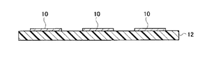
本発明の実施の形態に係る多層配線板は、図1に示すように、第1配線1、1a、第1絶縁層2、第2配線10、第2絶縁層12、接着層14、ビア絶縁体16、ビア導体18を備える。第1配線1、1aは、第1絶縁層2の一主面に配置される。第2配線10は、第2絶縁層12の一主面に配置される。接着層14は、第1絶縁層2の一主面と、第2絶縁層12の他の主面との間に配置される。ビア絶縁体16及びビア導体18は、接着層14と第2絶縁層12とを貫通して設けられる。
As shown in FIG. 1, the multilayer wiring board according to the embodiment of the present invention includes a
ビア絶縁体16は、第2配線10と、第2配線10に電気的に絶縁される第1配線1aとの間に配置される。ビア導体18は、第2配線10と、第2配線10に電気的に接続される第1配線1との間に配置される。
The
第1配線1の間のピッチは0.35mm〜0.45mmである。第2配線10のビア導体18が配置される部分は、配線中に設けられた径が250μm程度のランド等の電極部である。
The pitch between the
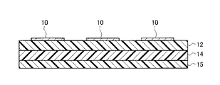
第1及び第2配線1、10として、銅等の低抵抗金属膜が用いられる。第1及び第2絶縁層2、12として、ポリイミド、液晶ポリマー等の厚さが30μm以下の樹脂フィルムが用いられる。接着層14として、エポキシ系等の熱硬化性樹脂フィルム、熱可塑性ポリイミド等の熱可塑性接着材、あるいは、ワニス等の流動性を有する樹脂が用いられる。
As the first and
ビア絶縁体16として、接着層14より大きな弾性係数を有する絶縁性フィラーを含有する絶縁性ペースト等を熱硬化した絶縁性部材が用いられる。絶縁性ペーストとしては、アルミナやホウ酸アルミニウム等の粒状の絶縁性フィラーとエポキシ樹脂とを混合したペーストが用いられる。絶縁性フィラーには、粒状のアクリル樹脂等が含まれてもよい。
As the
ビア導体18として、導電性ペースト等を熱硬化した導電性部材が用いられる。導電性ペーストとして、銀、金、銅、錫、ニッケル等の低抵抗金属フィラーを含有する導電性ペーストが用いられる。
As the
従来の多層配線板においては、図1に示したような電気的に接続されない第1配線1aと第2配線10の間にはビアが配置されない。また、電気的に接続される第1配線1と第2配線10の間にはビア導体18が配置される。ビア導体18には金属フィラーが含まれているので、流動性を有する樹脂から成る接着層14に比べて弾性係数が大きい。例えば、ビア導体18のヤング率は約10GPa〜約100GPaであるのに対し、接着層14のヤング率は1GPaより小さい。このような場合、導電性ペーストを熱硬化してビア導体18を形成すると、第1配線1の近傍ではビア導体18により表面の平坦性が保持される。一方、第1配線1aの上方では接着層14が流動するため、第1配線1aの上方に位置する第2配線10の近辺に歪による凹みが生じてしまう。そのため、回路部品をフリップチップ実装する場合、第1配線1aの上方の第2配線10に接続されるハンダバンプが形状不良となり、接続信頼性の高い実装が困難となる。
In the conventional multilayer wiring board, no via is arranged between the
一方、実施の形態に係る多層配線板では、図1に示したように、電気的に接続されない第1配線1aと第2配線10の間にビア絶縁体16が配置される。ビア絶縁体16には、アルミナやホウ酸アルミニウム等の絶縁性フィラーが含まれている。したがって、ビア絶縁体16の弾性係数は、接着層14より大きい。その結果、導電性ペーストの熱硬化の際に生じる歪を抑制することができる。
On the other hand, in the multilayer wiring board according to the embodiment, as shown in FIG. 1, the via
多層配線板表面の歪を抑制するためには、ビア絶縁体16の弾性係数は、ビア導体18と同じ程度の大きさが望ましい。即ち、ビア絶縁体16の弾性係数が、ビア導体18より小さければ、ビア絶縁体16近傍の表面に凹みが生じ、ビア導体18より大きければ、ビア絶縁体16近傍の表面に突起が生じる。ビア絶縁体16のヤング率は、ビア導体18のヤング率に対して、0.1倍〜10倍の範囲が望ましい。ビア絶縁体16のヤング率をビア導体18のヤング率に対して、0.1倍〜10倍の範囲とすることにより、ビア絶縁体16近傍の表面の平坦度が0.2%の許容範囲内に保持される。例えば、アルミナ90wt%、樹脂10wt%の絶縁性ペーストを用いることにより、上記範囲のビア絶縁体16を得ることができる。
In order to suppress the distortion on the surface of the multilayer wiring board, the elastic modulus of the via
このように、実施の形態によれば、ビア導体18が配置されない箇所にビア絶縁体16を配置することにより、多層配線板の表面に生じる歪を防止することができる。その結果、多層配線板表面の平坦性を保持することができ、実装される回路部品の接続信頼性を向上させることが可能となる。
As described above, according to the embodiment, by disposing the via
実施の形態に係る多層配線板の製造方法を、図2〜図10を参照して説明する。なお、出発材料として、厚さが約20μm〜30μmのポリイミドフィルムからなる第1及び第2絶縁層2、12の表面に銅箔を張り合わせた銅張積層板(CCL)が用いられる。
The manufacturing method of the multilayer wiring board which concerns on embodiment is demonstrated with reference to FIGS. As a starting material, a copper clad laminate (CCL) in which a copper foil is bonded to the surfaces of the first and second insulating
図2に示すように、第1絶縁層2の一主面に第1配線1、1aを形成する。例えば、第1絶縁層2に貼り合わされた銅箔の表面にレジストパターンを形成する。レジストパターンをマスクとして、ウェットエッチング等により銅箔を選択的に除去する。レジストパターンを除去して、第1配線1、1aが形成される。
As shown in FIG. 2,
図3に示すように、第2絶縁層12の一主面に第2配線10を形成する。例えば、第2絶縁層12に貼り合わされた銅箔の表面にレジストパターンを形成する。レジストパターンをマスクとして、ウェットエッチング等により銅箔を選択的に除去する。レジストパターンを除去して、第2配線10が形成される。
As shown in FIG. 3, the
図4に示すように、第2絶縁層12の他の主面に、約100℃で約30秒間の熱ラミネート等により、接着層14及びマスクフィルム15を積層する。接着層14は、例えば、厚さが約25μmの流動性を有する熱硬化性樹脂フィルムである。マスクフィルム15は導電性ペースト印刷用で、例えば、厚さが約25μmのポリイミドフィルムである。
As shown in FIG. 4, the
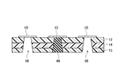
図5に示すように、所定の位置で、YAGレーザ等により、第2配線10の一部が露出するようにマスクフィルム15、接着層14、及び第2絶縁層12を貫通するダミービアホール56を形成する。ダミービアホール56は、第2配線10と電気的に絶縁される第1配線1aに対応する位置に形成される。
As shown in FIG. 5, dummy via
図6に示すように、スクリーン印刷等により、ダミービアホール56に絶縁性ペースト66を印刷して充填する。例えば、絶縁性ペースト66はアルミナ等の絶縁性フィラーとエポキシ樹脂とを90wt%/10wt%で混合したペーストである。
As shown in FIG. 6, an insulating
図7に示すように、所定の位置で、YAGレーザ等により、第2配線10の一部が露出するようにマスクフィルム15、接着層14、及び第2絶縁層12を貫通するビアホール58を形成する。ビアホール58は、第2配線10と電気的に接続される第1配線1に対応する位置に形成される。
As shown in FIG. 7, a via
図8に示すように、スクリーン印刷等により、ビアホール58に導電性ペースト68を印刷して充填する。例えば、導電性ペースト68は、銀等のはんだ材料を主成分とする導電性フィラーを含有する導電性ペーストである。
As shown in FIG. 8, a
図9に示すように、マスクフィルム15を除去する。そして、絶縁性ペースト66を第1配線1aに接触させる。同時に、導電性ペースト68を第1配線1に接触させる。
As shown in FIG. 9, the
図10に示すように、接着層14を第1絶縁層2に押圧しながら加熱することより、接着層14と第1絶縁層2を接着する。同時に、導電性ペースト68を硬化して第1配線1と第2配線10を電気的に接続するビア導体18を形成する。また、絶縁性ペースト66を硬化して第1配線1aと第2配線10の間にビア絶縁体16を形成する。このようにして、図1に示した多層配線板が製造される。
As shown in FIG. 10, the
上述のように、ビア絶縁体16の形成は、ビア導体18の形成工程に準じて行うことができる。したがって、新たな工程や装置は不要であり、ビア絶縁体16の形成工程による製造コストの増加を抑制することができる。また、図9に示した導電性ペースト68及び絶縁性ペースト66の接着層14から突出した部分は押圧されて、それぞれ第1配線1、1a上に広がる。
As described above, the formation of the via
硬化したビア絶縁体16及びビア導体18のヤング率は、それぞれ1GPa〜100GPaであり、接着層14より大きなヤング率を有する。したがって、多層配線基板の歪を低減して表面の平坦性を保持することができ、接続信頼性を向上させることが可能となる。
The cured via
また、多層配線板の歪みを低減できるため、接着層14に流動性の小さな材料を選定する必要がなくなる。そのため、一般的に用いられている既存の材料を使用することが可能となり、信頼性の低下や材料コストの増加を回避することができる。
Further, since distortion of the multilayer wiring board can be reduced, it is not necessary to select a material with low fluidity for the
また、上記説明では、ダミービアホール56に絶縁性ペースト66を充填後に、ビアホール58を形成しているが、ダミービアホール56の形成前にビアホール58を形成してもよい。この場合、形成したビアホール58に導電性ペースト68を充填した後に、ダミービアホール56が形成される。
In the above description, the via
また、第1及び第2絶縁層2、12として、液晶ポリマー等の熱可塑性基材を用いてもよい。熱可塑性基材は、押圧条件により流動性を生じさせることができる。そのため、例えば図1に示した接着層14を使用せず、第1及び第2絶縁層2、12を直接接着させた構成を用いることが可能となる。
Moreover, you may use thermoplastic base materials, such as a liquid crystal polymer, as the 1st and 2nd insulating
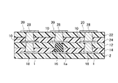
なお、実施の形態において、2層配線板を用いて説明したが、配線板の積層数は限定されず、3層以上の多層配線板であってもよい。例えば、図11に示すように、第2配線10を有する第2絶縁層12の上に、更に接着層24を介して第3配線20を有する第3絶縁層22を積層してもよい。第3配線20は、ビア導体28により第2配線10と電気的に接続される。また、図12に示すように、第3配線20と電気的に接続されない第2配線10aがある場合は、第3配線20と第2配線10aとの間にビア絶縁体26を配置すればよい。
In the embodiment, the description has been given by using the two-layer wiring board, but the number of wiring boards stacked is not limited, and may be a multilayer wiring board having three or more layers. For example, as shown in FIG. 11, a third insulating
(その他の実施の形態)
上記のように、本発明の実施の形態を記載したが、この開示の一部をなす論述及び図面はこの発明を限定するものであると理解すべきではない。この開示から当業者にはさまざまな代替実施の形態、実施例及び運用技術が明らかとなろう。したがって、本発明の技術的範囲は上記の説明から妥当な特許請求の範囲に係わる発明特定事項によってのみ定められるものである。
(Other embodiments)
Although the embodiments of the present invention have been described as described above, it should not be understood that the descriptions and drawings constituting a part of this disclosure limit the present invention. From this disclosure, various alternative embodiments, examples and operational techniques will be apparent to those skilled in the art. Accordingly, the technical scope of the present invention is defined only by the invention specifying matters according to the scope of claims reasonable from the above description.
本発明は、多層配線板及びその製造方法に適用することができる。 The present invention can be applied to a multilayer wiring board and a manufacturing method thereof.
1、1a…第1配線
2…第1絶縁層
10、10a…第2配線
12…第2絶縁層
14…接着層
15…マスクフィルム
16…ビア絶縁体
18…ビア導体
56…ダミービアホール
58…ビアホール
66…絶縁性ペースト
68…導電性ペースト
DESCRIPTION OF
Claims (3)
第2絶縁層の一主面に配置された第2配線と、
前記第1絶縁層の一主面及び前記第2絶縁層の他の主面の間に配置された接着層、並びに前記第2絶縁層を貫通して設けられ、前記第1及び第2配線の間に配置されたビア絶縁体と、
前記接着層、及び前記第2絶縁層を貫通して設けられ、前記第1及び第2配線を電気的に接続するビア導体とを備え、
前記ビア絶縁体及び前記ビア導体は、前記接着層より大きなヤング率を有することを特徴とする多層配線板。 A first wiring disposed on one main surface of the first insulating layer;
A second wiring disposed on one main surface of the second insulating layer;
An adhesive layer disposed between one main surface of the first insulating layer and the other main surface of the second insulating layer, and the second insulating layer; the first and second wirings; Via insulators disposed between;
A via conductor provided through the adhesive layer and the second insulating layer and electrically connecting the first and second wirings;
The multilayer wiring board, wherein the via insulator and the via conductor have a Young's modulus greater than that of the adhesive layer.
第2絶縁層の一主面に第2配線を形成する工程と、
前記第2絶縁層の他の主面に接着層及びマスクフィルムを積層する工程と、
前記第1配線の中で前記第2配線と電気的に絶縁される第1配線に対応する位置において、前記第2配線の一部が露出するように前記マスクフィルム、前記接着層及び前記第2絶縁層を貫通するダミービアホールを形成する工程と、
前記ダミービアホールに前記接着層より大きなヤング率を有する絶縁性フィラーを含有する絶縁性ペーストを充填する工程と、
前記第1配線の中で前記第2配線と電気的に接続される第1配線に対応する位置において、前記第2配線の一部が露出するように前記マスクフィルム、前記接着層及び前記第2絶縁層を貫通するビアホールを形成する工程と、
前記ビアホールに金属を含有する導電性ペーストを充填する工程と、
前記マスクフィルムを除去して、前記絶縁性ペースト及び前記導電性ペーストを、それぞれに対応する前記第1配線に接触させる工程と、
前記接着層を前記第1絶縁層に押圧しながら加熱することより、前記接着層と前記第1絶縁層を接着すると共に、前記導電性ペーストを硬化して前記第1及び第2配線を電気的に接続するビア導体を形成し、前記絶縁性ペーストを硬化して前記第1及び第2配線の間にビア絶縁体を形成する工程
とを含むことを特徴とする多層配線板の製造方法。 Forming a first wiring on one main surface of the first insulating layer;
Forming a second wiring on one main surface of the second insulating layer;
Laminating an adhesive layer and a mask film on the other main surface of the second insulating layer;
In the first wiring, the mask film, the adhesive layer, and the second so that a part of the second wiring is exposed at a position corresponding to the first wiring that is electrically insulated from the second wiring. Forming a dummy via hole penetrating the insulating layer;
Filling the dummy via hole with an insulating paste containing an insulating filler having a Young's modulus larger than that of the adhesive layer;
In the first wiring, the mask film, the adhesive layer, and the second so that a part of the second wiring is exposed at a position corresponding to the first wiring that is electrically connected to the second wiring. Forming a via hole penetrating the insulating layer;
Filling the via hole with a conductive paste containing metal;
Removing the mask film and bringing the insulating paste and the conductive paste into contact with the corresponding first wiring;
By heating the adhesive layer while pressing the adhesive layer against the first insulating layer, the adhesive layer and the first insulating layer are bonded, and the conductive paste is cured to electrically connect the first and second wirings. Forming a via conductor to be connected to the substrate and curing the insulating paste to form a via insulator between the first and second wirings.
Priority Applications (1)
| Application Number | Priority Date | Filing Date | Title |
|---|---|---|---|
| JP2011031975A JP2012174710A (en) | 2011-02-17 | 2011-02-17 | Multilayer wiring board and manufacturing method thereof |
Applications Claiming Priority (1)
| Application Number | Priority Date | Filing Date | Title |
|---|---|---|---|
| JP2011031975A JP2012174710A (en) | 2011-02-17 | 2011-02-17 | Multilayer wiring board and manufacturing method thereof |
Publications (1)
| Publication Number | Publication Date |
|---|---|
| JP2012174710A true JP2012174710A (en) | 2012-09-10 |
Family
ID=46977398
Family Applications (1)
| Application Number | Title | Priority Date | Filing Date |
|---|---|---|---|
| JP2011031975A Withdrawn JP2012174710A (en) | 2011-02-17 | 2011-02-17 | Multilayer wiring board and manufacturing method thereof |
Country Status (1)
| Country | Link |
|---|---|
| JP (1) | JP2012174710A (en) |
Cited By (3)
| Publication number | Priority date | Publication date | Assignee | Title |
|---|---|---|---|---|
| JP2015156435A (en) * | 2014-02-20 | 2015-08-27 | 株式会社村田製作所 | Resin multi-layered substrate |
| JPWO2016084375A1 (en) * | 2014-11-28 | 2017-09-07 | 日本ゼオン株式会社 | Manufacturing method of multilayer printed wiring board |
| JP2018152536A (en) * | 2017-03-15 | 2018-09-27 | ミツミ電機株式会社 | Method of manufacturing optical module and optical module |
-
2011
- 2011-02-17 JP JP2011031975A patent/JP2012174710A/en not_active Withdrawn
Cited By (4)
| Publication number | Priority date | Publication date | Assignee | Title |
|---|---|---|---|---|
| JP2015156435A (en) * | 2014-02-20 | 2015-08-27 | 株式会社村田製作所 | Resin multi-layered substrate |
| JPWO2016084375A1 (en) * | 2014-11-28 | 2017-09-07 | 日本ゼオン株式会社 | Manufacturing method of multilayer printed wiring board |
| US10568212B2 (en) | 2014-11-28 | 2020-02-18 | Intel Corporation | Manufacturing method for multi-layer printed circuit board |
| JP2018152536A (en) * | 2017-03-15 | 2018-09-27 | ミツミ電機株式会社 | Method of manufacturing optical module and optical module |
Similar Documents
| Publication | Publication Date | Title |
|---|---|---|
| JP3994262B2 (en) | Semiconductor device and manufacturing method thereof, circuit board, and electronic apparatus | |
| TWI483363B (en) | Package substrate, package structure and method for manufacturing package structure | |
| US20100014265A1 (en) | Flex-rigid wiring board and electronic device | |
| JPWO2007126090A1 (en) | CIRCUIT BOARD, ELECTRONIC DEVICE DEVICE, AND CIRCUIT BOARD MANUFACTURING METHOD | |
| JP2012079994A (en) | Component built-in printed circuit board and its manufacturing method | |
| JP2006108211A (en) | Wiring board, multilayered wiring circuit board using the board, and method of manufacturing the multilayered wiring circuit board | |
| JP2008226945A (en) | Semiconductor device and its manufacturing method | |
| US9351410B2 (en) | Electronic component built-in multi-layer wiring board and method of manufacturing the same | |
| US20170047230A1 (en) | Fabrication method of packaging substrate | |
| JP2014212141A (en) | Component built-in substrate, manufacturing method thereof, and package body | |
| JPWO2007069427A1 (en) | Electronic component built-in module and manufacturing method thereof | |
| JP2014146650A (en) | Wiring board and manufacturing method of the same | |
| TWI506758B (en) | Package on package structure and method for manufacturing same | |
| JP6423313B2 (en) | Electronic component built-in substrate, method for manufacturing the same, and electronic apparatus | |
| JP2012174710A (en) | Multilayer wiring board and manufacturing method thereof | |
| JP2009289790A (en) | Printed wiring board with built-in component and its manufacturing method | |
| JP6105316B2 (en) | Electronic equipment | |
| US20200203266A1 (en) | Substrate, method of manufacturing substrate, and electronic device | |
| JP2009260165A (en) | Semiconductor device | |
| JP2013093366A (en) | Flexible wiring board and manufacturing method of the same | |
| KR102052761B1 (en) | Chip Embedded Board And Method Of Manufacturing The Same | |
| JP2016100352A (en) | Printed wiring board and manufacturing method of the same | |
| KR20070030700A (en) | Electronic component embedded board and its manufacturing method | |
| JPWO2019230524A1 (en) | Resin multilayer board and electronic equipment | |
| TW201427505A (en) | Printed circuit board having buried component and method for manufacturing same |
Legal Events
| Date | Code | Title | Description |
|---|---|---|---|
| A300 | Withdrawal of application because of no request for examination |
Free format text: JAPANESE INTERMEDIATE CODE: A300 Effective date: 20140513 |