JP2012164785A - Imprint device, and article manufacturing method - Google Patents
Imprint device, and article manufacturing method Download PDFInfo
- Publication number
- JP2012164785A JP2012164785A JP2011023516A JP2011023516A JP2012164785A JP 2012164785 A JP2012164785 A JP 2012164785A JP 2011023516 A JP2011023516 A JP 2011023516A JP 2011023516 A JP2011023516 A JP 2011023516A JP 2012164785 A JP2012164785 A JP 2012164785A
- Authority
- JP
- Japan
- Prior art keywords
- gas
- imprint apparatus
- imprint
- substrate
- refractive index
- Prior art date
- Legal status (The legal status is an assumption and is not a legal conclusion. Google has not performed a legal analysis and makes no representation as to the accuracy of the status listed.)
- Granted
Links
- 238000004519 manufacturing process Methods 0.000 title claims description 12
- 239000000758 substrate Substances 0.000 claims abstract description 29
- 239000000463 material Substances 0.000 claims abstract description 13
- 238000002156 mixing Methods 0.000 claims abstract description 5
- 238000000465 moulding Methods 0.000 claims abstract description 5
- 239000007789 gas Substances 0.000 claims description 131
- 238000005259 measurement Methods 0.000 claims description 19
- 230000003287 optical effect Effects 0.000 claims description 12
- 238000011084 recovery Methods 0.000 claims description 9
- 239000001307 helium Substances 0.000 claims description 7
- 229910052734 helium Inorganic materials 0.000 claims description 7
- SWQJXJOGLNCZEY-UHFFFAOYSA-N helium atom Chemical compound [He] SWQJXJOGLNCZEY-UHFFFAOYSA-N 0.000 claims description 7
- 238000012545 processing Methods 0.000 claims description 5
- 230000001678 irradiating effect Effects 0.000 claims description 4
- UFHFLCQGNIYNRP-UHFFFAOYSA-N Hydrogen Chemical compound [H][H] UFHFLCQGNIYNRP-UHFFFAOYSA-N 0.000 claims description 3
- 239000001257 hydrogen Substances 0.000 claims description 3
- 229910052739 hydrogen Inorganic materials 0.000 claims description 3
- 230000007261 regionalization Effects 0.000 abstract description 7
- 239000000203 mixture Substances 0.000 abstract description 2
- 239000011347 resin Substances 0.000 description 36
- 229920005989 resin Polymers 0.000 description 36
- 238000000034 method Methods 0.000 description 17
- 238000006073 displacement reaction Methods 0.000 description 9
- MSSNHSVIGIHOJA-UHFFFAOYSA-N pentafluoropropane Chemical compound FC(F)CC(F)(F)F MSSNHSVIGIHOJA-UHFFFAOYSA-N 0.000 description 7
- 238000005286 illumination Methods 0.000 description 6
- 238000003825 pressing Methods 0.000 description 6
- 230000005484 gravity Effects 0.000 description 4
- 238000000016 photochemical curing Methods 0.000 description 4
- 239000004065 semiconductor Substances 0.000 description 4
- 239000011248 coating agent Substances 0.000 description 3
- 238000000576 coating method Methods 0.000 description 3
- 238000001723 curing Methods 0.000 description 2
- 238000005516 engineering process Methods 0.000 description 2
- 238000005530 etching Methods 0.000 description 2
- 239000012466 permeate Substances 0.000 description 2
- 238000007796 conventional method Methods 0.000 description 1
- 238000012937 correction Methods 0.000 description 1
- 230000007547 defect Effects 0.000 description 1
- 238000010586 diagram Methods 0.000 description 1
- 239000011521 glass Substances 0.000 description 1
- 239000004973 liquid crystal related substance Substances 0.000 description 1
- 229910021421 monocrystalline silicon Inorganic materials 0.000 description 1
- 238000000206 photolithography Methods 0.000 description 1
- 239000000047 product Substances 0.000 description 1
- 239000010453 quartz Substances 0.000 description 1
- 238000004064 recycling Methods 0.000 description 1
- VYPSYNLAJGMNEJ-UHFFFAOYSA-N silicon dioxide Inorganic materials O=[Si]=O VYPSYNLAJGMNEJ-UHFFFAOYSA-N 0.000 description 1
- 238000012546 transfer Methods 0.000 description 1
- 230000009466 transformation Effects 0.000 description 1
Images

Classifications
-
- B—PERFORMING OPERATIONS; TRANSPORTING
- B82—NANOTECHNOLOGY
- B82Y—SPECIFIC USES OR APPLICATIONS OF NANOSTRUCTURES; MEASUREMENT OR ANALYSIS OF NANOSTRUCTURES; MANUFACTURE OR TREATMENT OF NANOSTRUCTURES
- B82Y10/00—Nanotechnology for information processing, storage or transmission, e.g. quantum computing or single electron logic
-
- B—PERFORMING OPERATIONS; TRANSPORTING
- B29—WORKING OF PLASTICS; WORKING OF SUBSTANCES IN A PLASTIC STATE IN GENERAL
- B29C—SHAPING OR JOINING OF PLASTICS; SHAPING OF MATERIAL IN A PLASTIC STATE, NOT OTHERWISE PROVIDED FOR; AFTER-TREATMENT OF THE SHAPED PRODUCTS, e.g. REPAIRING
- B29C43/00—Compression moulding, i.e. applying external pressure to flow the moulding material; Apparatus therefor
- B29C43/32—Component parts, details or accessories; Auxiliary operations
- B29C43/56—Compression moulding under special conditions, e.g. vacuum
-
- B—PERFORMING OPERATIONS; TRANSPORTING
- B29—WORKING OF PLASTICS; WORKING OF SUBSTANCES IN A PLASTIC STATE IN GENERAL
- B29C—SHAPING OR JOINING OF PLASTICS; SHAPING OF MATERIAL IN A PLASTIC STATE, NOT OTHERWISE PROVIDED FOR; AFTER-TREATMENT OF THE SHAPED PRODUCTS, e.g. REPAIRING
- B29C33/00—Moulds or cores; Details thereof or accessories therefor
-
- B—PERFORMING OPERATIONS; TRANSPORTING
- B29—WORKING OF PLASTICS; WORKING OF SUBSTANCES IN A PLASTIC STATE IN GENERAL
- B29C—SHAPING OR JOINING OF PLASTICS; SHAPING OF MATERIAL IN A PLASTIC STATE, NOT OTHERWISE PROVIDED FOR; AFTER-TREATMENT OF THE SHAPED PRODUCTS, e.g. REPAIRING
- B29C43/00—Compression moulding, i.e. applying external pressure to flow the moulding material; Apparatus therefor
- B29C43/02—Compression moulding, i.e. applying external pressure to flow the moulding material; Apparatus therefor of articles of definite length, i.e. discrete articles
- B29C43/021—Compression moulding, i.e. applying external pressure to flow the moulding material; Apparatus therefor of articles of definite length, i.e. discrete articles characterised by the shape of the surface
-
- B—PERFORMING OPERATIONS; TRANSPORTING
- B29—WORKING OF PLASTICS; WORKING OF SUBSTANCES IN A PLASTIC STATE IN GENERAL
- B29C—SHAPING OR JOINING OF PLASTICS; SHAPING OF MATERIAL IN A PLASTIC STATE, NOT OTHERWISE PROVIDED FOR; AFTER-TREATMENT OF THE SHAPED PRODUCTS, e.g. REPAIRING
- B29C59/00—Surface shaping of articles, e.g. embossing; Apparatus therefor
- B29C59/02—Surface shaping of articles, e.g. embossing; Apparatus therefor by mechanical means, e.g. pressing
- B29C59/026—Surface shaping of articles, e.g. embossing; Apparatus therefor by mechanical means, e.g. pressing of layered or coated substantially flat surfaces
-
- B—PERFORMING OPERATIONS; TRANSPORTING
- B82—NANOTECHNOLOGY
- B82Y—SPECIFIC USES OR APPLICATIONS OF NANOSTRUCTURES; MEASUREMENT OR ANALYSIS OF NANOSTRUCTURES; MANUFACTURE OR TREATMENT OF NANOSTRUCTURES
- B82Y40/00—Manufacture or treatment of nanostructures
-
- G—PHYSICS
- G03—PHOTOGRAPHY; CINEMATOGRAPHY; ANALOGOUS TECHNIQUES USING WAVES OTHER THAN OPTICAL WAVES; ELECTROGRAPHY; HOLOGRAPHY
- G03F—PHOTOMECHANICAL PRODUCTION OF TEXTURED OR PATTERNED SURFACES, e.g. FOR PRINTING, FOR PROCESSING OF SEMICONDUCTOR DEVICES; MATERIALS THEREFOR; ORIGINALS THEREFOR; APPARATUS SPECIALLY ADAPTED THEREFOR
- G03F7/00—Photomechanical, e.g. photolithographic, production of textured or patterned surfaces, e.g. printing surfaces; Materials therefor, e.g. comprising photoresists; Apparatus specially adapted therefor
- G03F7/0002—Lithographic processes using patterning methods other than those involving the exposure to radiation, e.g. by stamping
-
- B—PERFORMING OPERATIONS; TRANSPORTING
- B29—WORKING OF PLASTICS; WORKING OF SUBSTANCES IN A PLASTIC STATE IN GENERAL
- B29C—SHAPING OR JOINING OF PLASTICS; SHAPING OF MATERIAL IN A PLASTIC STATE, NOT OTHERWISE PROVIDED FOR; AFTER-TREATMENT OF THE SHAPED PRODUCTS, e.g. REPAIRING
- B29C43/00—Compression moulding, i.e. applying external pressure to flow the moulding material; Apparatus therefor
- B29C43/32—Component parts, details or accessories; Auxiliary operations
- B29C43/56—Compression moulding under special conditions, e.g. vacuum
- B29C2043/566—Compression moulding under special conditions, e.g. vacuum in a specific gas atmosphere, with or without pressure
-
- B—PERFORMING OPERATIONS; TRANSPORTING
- B29—WORKING OF PLASTICS; WORKING OF SUBSTANCES IN A PLASTIC STATE IN GENERAL
- B29C—SHAPING OR JOINING OF PLASTICS; SHAPING OF MATERIAL IN A PLASTIC STATE, NOT OTHERWISE PROVIDED FOR; AFTER-TREATMENT OF THE SHAPED PRODUCTS, e.g. REPAIRING
- B29C59/00—Surface shaping of articles, e.g. embossing; Apparatus therefor
- B29C59/16—Surface shaping of articles, e.g. embossing; Apparatus therefor by wave energy or particle radiation, e.g. infrared heating
-
- B—PERFORMING OPERATIONS; TRANSPORTING
- B29—WORKING OF PLASTICS; WORKING OF SUBSTANCES IN A PLASTIC STATE IN GENERAL
- B29K—INDEXING SCHEME ASSOCIATED WITH SUBCLASSES B29B, B29C OR B29D, RELATING TO MOULDING MATERIALS OR TO MATERIALS FOR MOULDS, REINFORCEMENTS, FILLERS OR PREFORMED PARTS, e.g. INSERTS
- B29K2101/00—Use of unspecified macromolecular compounds as moulding material
-
- B—PERFORMING OPERATIONS; TRANSPORTING
- B29—WORKING OF PLASTICS; WORKING OF SUBSTANCES IN A PLASTIC STATE IN GENERAL
- B29L—INDEXING SCHEME ASSOCIATED WITH SUBCLASS B29C, RELATING TO PARTICULAR ARTICLES
- B29L2031/00—Other particular articles
- B29L2031/34—Electrical apparatus, e.g. sparking plugs or parts thereof
Abstract
Description
本発明は、インプリント装置、および、物品の製造方法に関する。 The present invention relates to an imprint apparatus and an article manufacturing method.
半導体デバイスの微細化の要求が進み、従来のフォトリソグラフィ技術に加え、基板上の未硬化樹脂をモールド(型)で成形し、樹脂のパターンを基板上に形成する微細加工技術が注目を集めている。この技術は、インプリント技術とも呼ばれ、基板上に数ナノメートルオーダーの微細な構造体を形成することができる。例えば、インプリント技術の一つとして、光硬化法がある。この光硬化法を採用したインプリント装置では、まず、基板(ウエハ)上のショット領域(インプリント領域)に紫外線硬化樹脂(インプリント樹脂、光硬化樹脂)を塗布する。次に、この樹脂(未硬化樹脂)をモールドにより成形する。そして、紫外線を照射して樹脂を硬化させたうえで離型することにより、樹脂のパターンが基板上に形成される。 The demand for miniaturization of semiconductor devices has advanced, and in addition to conventional photolithography technology, microfabrication technology that forms uncured resin on a substrate with a mold and forms a resin pattern on the substrate attracts attention. Yes. This technique is also called an imprint technique, and can form a fine structure on the order of several nanometers on a substrate. For example, as one of imprint techniques, there is a photocuring method. In an imprint apparatus employing this photocuring method, first, an ultraviolet curable resin (imprint resin, photocurable resin) is applied to a shot area (imprint area) on a substrate (wafer). Next, this resin (uncured resin) is molded by a mold. Then, the resin pattern is formed on the substrate by irradiating ultraviolet rays to cure the resin and then releasing the mold.
このインプリント装置では、一般に装置内の雰囲気が大気であるため、モールドと樹脂とを互いに押し付けるとその間に大気が留まり、残留ガスとなって樹脂に気泡が混入するなど転写されるパターンに不具合が生じ、正確なパターン形成ができない場合がある。これに対して、残留ガスが樹脂やモールドに溶解、拡散、または透過して消滅するまで待機する方法もあるが、インプリント工程に多大な時間を要する。そこで、例えば、特許文献1は、インプリント雰囲気に透過性ガスを使用し、樹脂やモールドに残留した透過性ガスを溶解または拡散させることで、残留ガスを素早く減少させるインプリント装置を開示している。一方、特許文献2は、インプリント雰囲気にモールドと樹脂とを押し付けた際の圧力上昇により凝縮する凝縮性ガスを使用したインプリント装置を開示している。この凝縮性ガスは、残留時には液化して、気体時に比べて体積が数百分の1にまで小さくなるので、残留ガスのパターン形成への影響を抑えることができる。
In this imprint apparatus, since the atmosphere in the apparatus is generally the air, when the mold and the resin are pressed against each other, the air stays between them, and there is a defect in the transferred pattern such as bubbles remaining in the resin as a residual gas. And accurate pattern formation may not be possible. On the other hand, there is a method of waiting until the residual gas dissolves, diffuses or permeates in the resin or mold and disappears, but the imprint process takes a long time. Therefore, for example,
しかしながら、特許文献1、2に示すインプリント装置では、インプリント雰囲気全体を透過性ガスまたは凝縮性ガスでパージするため、コスト面で不利である。また、インプリント装置は、通常、干渉変位測定手段を使用して、適宜移動するウエハステージなどの位置を正確に計測している。この測定手段は、測定ビーム(光)を用いるため、通過する媒体(雰囲気)の組成の変化や圧力および温度の変化に非常に敏感である。したがって、例えば、基板上の樹脂の周囲を大気と異なる屈折率のガスでパージした場合、このガスが測定手段の光路に進入すると、干渉変位測定を正確に実施することができない。ここで、透過性ガスは、比重が大気よりも小さく、屈折率が大気に比べて小さい。したがって、透過性ガスが測定ビームの光路に進入すると、媒体の屈折率が小さくなり、干渉変位測定が不安定となる。一方、凝縮性ガスは、比重が大気よりも大きく、屈折率が大気に比べて大きい。したがって、凝縮性ガスが測定ビームの光路に進入すると、媒体の屈折率が大きくなり、この場合も干渉変位測定が不安定となる。干渉変位測定が不安定になるとウエハステージなどの位置決めが不安定となり、その結果、転写されるパターンの位置が目標位置からずれるなど正確なパターン形成ができない場合がある。
However, the imprint apparatuses shown in
本発明は、正確なパターン形成とスループットとの両立に有利なインプリント装置を提供することを目的とする。 An object of the present invention is to provide an imprint apparatus that is advantageous for achieving both accurate pattern formation and throughput.
上記課題を解決するために、本発明は、基板上のインプリント材を型により成形して硬化させ、基板上にパターンを形成するインプリント装置であって、基板上のインプリント材と型との間にガスを供給する供給手段を有し、供給手段は、型、インプリント材および基板の少なくとも1つを透過する透過性ガスと、成形により生じる圧力により液化する凝縮性ガスとを混合した混合ガスを供給することを特徴とする。 In order to solve the above-described problems, the present invention provides an imprint apparatus for forming a pattern on a substrate by molding the imprint material on the substrate with a mold and curing the imprint material on the substrate. The gas supply means has a supply means for supplying a gas, and the supply means mixed a permeable gas that permeates at least one of the mold, the imprint material, and the substrate with a condensable gas that is liquefied by pressure generated by molding. A mixed gas is supplied.
本発明によれば、例えば、正確なパターン形成とスループットとの両立に有利なインプリント装置を提供することができる。 According to the present invention, for example, it is possible to provide an imprint apparatus that is advantageous for achieving both accurate pattern formation and throughput.
以下、本発明を実施するための形態について図面等を参照して説明する。 Hereinafter, embodiments for carrying out the present invention will be described with reference to the drawings.
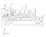
まず、本発明の一実施形態に係るインプリント装置の構成について説明する。図1は、本実施形態のインプリント装置の構成を示す図である。このインプリント装置は、半導体デバイス等のデバイスの製造に使用され、被処理体であるウエハ上(基板上)のインプリント材(典型的には未硬化樹脂)をモールド(型)で成形し、パターン(典型的には樹脂のパターン)を基板上に形成する装置である。なお、ここでは光硬化法を採用したインプリント装置としている。また、以下の図においては、基板上の樹脂に対して紫外線を照射する照明系の光軸に平行にZ軸を取り、Z軸に垂直な平面内に互いに直交するX軸およびY軸を取っている。このインプリント装置1は、照明系2と、モールド保持部3と、ウエハステージ4と、塗布部5と、ガス供給部6と、制御部7とを備える。
First, the configuration of an imprint apparatus according to an embodiment of the present invention will be described. FIG. 1 is a diagram illustrating a configuration of an imprint apparatus according to the present embodiment. This imprint apparatus is used for manufacturing a device such as a semiconductor device, and forms an imprint material (typically uncured resin) on a wafer (on a substrate), which is an object to be processed, with a mold (mold). An apparatus for forming a pattern (typically a resin pattern) on a substrate. Here, the imprint apparatus adopts a photocuring method. In the following figure, the Z axis is taken in parallel to the optical axis of the illumination system that irradiates the resin on the substrate with ultraviolet rays, and the X axis and the Y axis perpendicular to each other are taken in a plane perpendicular to the Z axis. ing. The
照明系2は、インプリント処理の際に、モールド8に対して紫外線を照射する照明手段である。この照明系2は、不図示であるが、光源と、該光源から射出された紫外線をインプリントに適切な光に調整するための光学素子とから構成される。また、モールド8は、ウエハ10に対向する面に所定のパターン(例えば、回路パターンに対応する凹凸パターン)が3次元状に形成された型である。なお、モールド8の材質は、石英等、紫外線を透過させることが可能な材料である。
The illumination system 2 is illumination means for irradiating the
モールド保持部3は、真空吸着力や静電力によりモールド8を引きつけて保持する保持部である。このモールド保持部3は、モールドチャック9と、ウエハ10上に塗布された紫外線硬化樹脂にモールド8を押し付けるためにモールド保持部3をZ軸方向に駆動する不図示のモールド駆動機構とを含む。なお、インプリント装置1における押型および離型動作は、このようにモールド8をZ方向に移動させることで実現してもよいが、例えば、ウエハステージ4(ウエハ10)をZ方向に移動させることで実現してもよく、または、その双方を移動させてもよい。
The mold holding unit 3 is a holding unit that attracts and holds the
ウエハステージ4は、ウエハ10を例えば真空吸着により保持し、かつ、XY平面内を可動とするウエハチャック11を備えた保持部である。ここで、ウエハ10は、例えば、単結晶シリコンからなる被処理体であり、この被処理面には、モールド8により成形される紫外線硬化樹脂(以下、単に「樹脂」と表記する)が塗布される。また、ウエハステージ4は、その周囲に、その6自由度(X、Y、Z、ωx、ωy、ωz)の位置を制御できるように複数の参照ミラー(反射部)13を備える。インプリント装置1は、これらの参照ミラー13にそれぞれビームを照射することでウエハステージ4の位置を測定する複数のレーザー干渉計(測定手段)14を備える。レーザー干渉計14は、ウエハステージ4の位置をリアルタイムで計測し、後述する制御部7は、この計測値に基づいてウエハ10(ウエハステージ4)の位置決め制御を実行する。
The wafer stage 4 is a holding unit including a
塗布部5は、ウエハ10上に樹脂12(未硬化樹脂)を塗布する塗布手段である。ここで、樹脂12は、紫外線を受光することにより硬化する性質を有する光硬化樹脂(インプリント材)であって、半導体デバイスの製造工程等により適宜選択される。
The
ガス供給部6は、モールド8とウエハ10上の樹脂12とを互いに押し付ける押型動作の際に、その押型位置に向かって混合ガスを供給する供給手段(供給部)である。このガス供給部6は、まず、モールド8、樹脂12、またはウエハ10の少なくとも1つに対して溶解または拡散する性質を有する透過性ガスを供給する透過性ガス供給部20を含む。また、ガス供給部6は、圧力を加えられること(圧力上昇)で凝縮し、液化する性質を有する凝縮性ガスを供給する凝縮性ガス供給部21を含む。ここで、透過性ガスとしては、ヘリウムや水素などのガスが採用可能である。ただし、透過性ガスとして可燃性の水素を使用する場合には、インプリント装置1内に防爆システムを別途設置し、火気に注意した構成とする必要がある。一方、凝縮性ガスとしては、HFC−245fa(1、1、1、3、3ペンタフルオロプロパン、CHF2CH2CF3)を代表とするHFC(ハイドロフルオロカーボン)が採用可能である。ただし、凝縮性ガスに採用するガスは、これに限らず、例えばHFE−245mc(CF3CF2OCH3)を代表とするHFE(ハイドロフルオロエーテル)などでもよい。また、ガス供給部6は、透過性ガス供給部20と凝縮性ガス供給部21とから供給されたそれぞれガスを混合するガス混合部22と、第1バルブ23と第2バルブ24とによりガス混合部22に供給する各ガスの供給量を制御するガス供給制御部25とを含む。ガス供給制御部25は、ガス混合部22にて各ガスを所望の成分比に混合し、生成された混合ガスを、第3バルブ26を制御することで供給量を調整しつつ、ガス供給ノズル27からモールド8とウエハ10とに挟まれた押型位置に供給させる調整部である。なお、このガス供給制御部25は、インプリント装置1内に単体で設置し、後述の制御部7と回線を介して接続される構成としてもよいし、または制御部7と一体で構成してもよい。
The gas supply unit 6 is a supply unit (supply unit) that supplies a mixed gas toward the mold position when performing a mold operation for pressing the
制御部7は、インプリント装置1の各構成要素の動作および調整等を制御しうる。制御部7は、例えば、コンピュータ等で構成され、インプリント装置1の各構成要素に回線を介して接続され、プログラム等にしたがって各構成要素の制御を実行しうる。本実施形態では、制御部7は、モールド保持部3やウエハステージ4などの動作に加え、少なくともレーザー干渉計14やガス供給制御部25の処理動作を制御する。なお、制御部7は、インプリント装置1の他の部分と一体で構成してもよいし、インプリント装置1の他の部分とは別の場所に設置してもよい。
The
次に、インプリント装置1によるインプリント処理について説明する。まず、制御部7は、不図示の基板搬送装置によりウエハステージ4にウエハ10を載置および固定させた後、ウエハステージ4を塗布部5の塗布位置へ移動させる。その後、塗布部5は、塗布工程としてウエハ10の所定のショット(インプリント領域)に樹脂(未硬化樹脂)12を塗布する。次に、制御部7は、ウエハ10上の当該ショットがモールド8の直下に位置するように、ウエハステージ4を移動させる。次に、制御部7は、モールド8とウエハ10上の当該ショットとの位置合わせ、および不図示の倍率補正機構によるモールド8の倍率補正などを実施した後、モールド駆動機構を駆動させ、ウエハ10上の樹脂12にモールド8を押し付ける(押型工程)。この押型により、樹脂12は、モールド8に形成された凹部に充填される。この状態で、照明系2は、硬化工程としてモールド8の背面(上面)から紫外線を照射し、モールド8を透過した紫外線により樹脂を硬化させる。そして、樹脂12が硬化した後、制御部7は、モールド駆動機構を再駆動させ、モールド8をウエハ10から引き離す(離型工程)。これにより、ウエハ10上のショットの表面には、凹凸パターンに倣った3次元形状の樹脂12の層が形成される。
Next, imprint processing by the
特に、本実施形態の押型工程では、制御部7は、ガス供給部6により押型位置に対して透過性ガスと凝縮性ガスとの混合ガスを供給させる。図2は、レーザー干渉計14の測定ビーム波長と、大気、透過性ガス、凝縮性ガス、および該透過性ガスと該凝縮性ガスとの混合ガスの各雰囲気の屈折率との関係を示すグラフである。なお、ここでは透過性ガスをヘリウムガスとし、凝縮性ガスをHFC−245faガスとしている。上述のとおり、透過性ガスは、分子径が小さい場合が一般的であり、屈折率が大気に比べて小さく、一方、凝縮性ガスの屈折率は、大気に比べて大きい。したがって、1気圧において、大気の屈折率をnairとし、透過性ガスの屈折率をn1とし、また、凝縮性ガスの屈折率をn2とすると、以下の式(1)に示す関係が成り立つ。
n1<nair<n2 (1)
さらに、1気圧における透過性ガスと凝縮性ガスとの混合ガスの屈折率をn3とした場合、透過性ガスと大気との屈折率差をΔn1とし、凝縮性ガスと大気との屈折率差をΔn2とし、また、混合ガスと大気との屈折率差をΔn3とする。ここで、押型位置に対して供給するガスとして透過性ガスのみを使用する場合に比べて、混合ガスを使用した方がその周囲の大気の屈折率との差異が小さくなり、干渉変位測定への影響を抑えることができるのは、以下の式(2)に示す関係が成り立つ場合である。
|Δn1|>|Δn3| (2)
一方、押型位置に対して供給するガスとして凝縮性ガスのみを使用する場合に比べて、混合ガスを使用した方がその周囲の大気の屈折率との差異が小さくなり、干渉変位測定への影響を抑えることができるのは、以下の式(3)に示す関係が成り立つ場合である。
|Δn2|>|Δn3| (3)
なお、式(2)および(3)では、各屈折率差は、絶対値とする。すなわち、式(1)の条件を満足する透過性ガスと凝縮性ガスとを使用すれば、必然的に式(2)および式(3)の条件を満足するので、この場合、透過性ガスまたは凝縮性ガスを単独で使用する場合に比べて、干渉変位測定への影響を抑えることができる。
In particular, in the stamping process of the present embodiment, the
n 1 <n air <n 2 (1)
Further, when the refractive index of the mixed gas of the permeable gas and the condensable gas at 1 atmosphere is n 3 , the refractive index difference between the permeable gas and the atmosphere is Δn 1 , and the refractive index between the condensable gas and the atmosphere is The difference is Δn 2 , and the refractive index difference between the mixed gas and the atmosphere is Δn 3 . Here, compared with the case where only permeable gas is used as the gas supplied to the pressing position, the difference between the refractive index of the surrounding atmosphere is smaller when the mixed gas is used, and the interference displacement measurement is reduced. The influence can be suppressed when the relationship shown in the following formula (2) is established.
| Δn 1 | >> | Δn 3 | (2)
On the other hand, compared to the case where only condensable gas is used as the gas to be supplied to the mold position, the difference in the refractive index of the surrounding atmosphere is smaller when the mixed gas is used, which affects the interference displacement measurement. Can be suppressed when the relationship shown in the following equation (3) holds.
| Δn 2 | >> | Δn 3 | (3)
In equations (2) and (3), each refractive index difference is an absolute value. That is, if a permeable gas and a condensable gas that satisfy the condition of the formula (1) are used, the conditions of the formula (2) and the formula (3) are inevitably satisfied. Compared to the case where a condensable gas is used alone, the influence on the interference displacement measurement can be suppressed.
また、このように透過性ガスと凝縮性ガスとの混合ガスを押型位置に供給する場合、インプリント装置1内に2箇所のガス回収ノズル30、31を設置してもよい。図1に示すように、レーザー干渉計14の光路は、ウエハチャック11の上面より低い位置にある。ここで、混合ガス中のHFC−245faは、ヘリウムと大気とに比べて比重が大きいので、混合ガスから分離して干渉変位測定領域(光路)に進入しやすい。そこで、ヘリウムの成分比率は、大気と同じ屈折率となる比率よりやや高くなるように設定してもよい。その場合、供給する混合ガスの屈折率は、大気のそれよりも小さい。また、インプリント装置1は、重力方向に押型位置よりも高い位置に第1ガス回収ノズル30を設置し、一方、押型位置よりも低い位置に第2ガス回収ノズル31を備える。ガス回収ノズル30、31は、それぞれ第1および第2ガス回収部32、33に接続される。この構成により、第1ガス回収部32で回収されたガスは、ヘリウムの存在比が高くなり、一方、第2ガス回収部33で回収されたガスは、HFC−245faの存在比が高くなる。したがって、インプリント装置1内で分離したヘリウムとHFC−245faとを効率良く回収することができるので、ガスのリサイクルに有利である。なお、例えば、レーザー干渉計14の光路がウエハチャック11の上面より高い位置にある場合には、HFC−245faの成分比率は、大気と同じ屈折率となる比率よりやや高くなるように設定してもよい。その場合、供給する混合ガスの屈折率は、大気のそれよりも大きい。
Further, when supplying a mixed gas of a permeable gas and a condensable gas to the stamping position in this way, two
さらに、制御部7は、ウエハステージ4を既知の位置に配置した状態でのレーザー干渉計14の出力に基づいて、混合ガスの成分比を調整させてもよい。例えば、制御部7は、混合ガスの供給時の測定値が、上記出力に基づいた許容範囲を超えた場合には、ガス供給制御部25に対して、混合ガスの成分比を変更させるように指示する。一方、測定ビームの光路雰囲気の気体成分を検出する検出器をインプリント装置1内に設置して、検出された気体成分において凝縮性ガスの成分値が許容範囲を超えた場合、制御部7がガス供給制御部25に対して混合ガスの成分比を変更させる構成としてもよい。この場合の検出器には、これと付随して気体成分を分析する分析装置を設置してもよい。ここで、上記許容範囲は、装置構成および寸法、またはこれまでのインプリント処理の実績など考慮して決定しうる。これにより、例えば、混合ガスの供給時に混合ガスから分離した凝縮性ガスなどが測定ビームの光路に進入し、レーザー干渉計14の出力に影響が出た場合でも、即座に対応することができる。
Further, the
以上のように、本実施形態によれば、モールド8と樹脂12との間に残留するガスを短時間で低減させつつ、レーザー干渉計14による測定を正確に実施することができる。したがって、正確なパターン形成とスループットとの両立に有利なインプリント装置を提供することができる。
As described above, according to the present embodiment, the measurement by the
(物品の製造方法)
物品としてのデバイス(半導体集積回路素子、液晶表示素子等)の製造方法は、上述したインプリント装置を用いて基板(ウエハ、ガラスプレート、フィルム状基板)にパターンを形成する工程を含む。さらに、該製造方法は、パターンを形成された基板をエッチングする工程を含みうる。なお、パターンドメディア(記録媒体)や光学素子等の他の物品を製造する場合には、該製造方法は、エッチングの代わりに、パターンを形成された基板を加工する他の処理を含みうる。本実施形態の物品の製造方法は、従来の方法に比べて、物品の性能・品質・生産性・生産コストの少なくとも1つにおいて有利である。
(Product manufacturing method)
A method for manufacturing a device (semiconductor integrated circuit element, liquid crystal display element, etc.) as an article includes a step of forming a pattern on a substrate (wafer, glass plate, film-like substrate) using the above-described imprint apparatus. Furthermore, the manufacturing method may include a step of etching the substrate on which the pattern is formed. In the case of manufacturing other articles such as patterned media (recording media) and optical elements, the manufacturing method may include other processing for processing a substrate on which a pattern is formed instead of etching. The method for manufacturing an article according to the present embodiment is advantageous in at least one of the performance, quality, productivity, and production cost of the article as compared with the conventional method.
以上、本発明の好ましい実施形態について説明したが、本発明は、これらの実施形態に限定されず、その要旨の範囲内で種々の変形および変更が可能である。 As mentioned above, although preferable embodiment of this invention was described, this invention is not limited to these embodiment, A various deformation | transformation and change are possible within the range of the summary.
1 インプリント装置
6 ガス供給部
8 モールド
10 ウエハ
12 樹脂
DESCRIPTION OF
Claims (9)
前記基板上の前記インプリント材と前記型との間にガスを供給する供給手段を有し、
前記供給手段は、前記型、前記インプリント材および前記基板の少なくとも1つを透過する透過性ガスと、前記成形により生じる圧力により液化する凝縮性ガスとを混合した混合ガスを供給する、
ことを特徴とするインプリント装置。 An imprint apparatus that molds and cures an imprint material on a substrate with a mold, and forms a pattern on the substrate,
Supply means for supplying gas between the imprint material on the substrate and the mold;
The supply means supplies a mixed gas obtained by mixing a permeable gas that passes through at least one of the mold, the imprint material, and the substrate, and a condensable gas that is liquefied by pressure generated by the molding.
An imprint apparatus characterized by that.
前記保持部に光を照射して前記保持部の位置を測定する測定手段と、を有し、
前記混合ガスの屈折率と大気の屈折率との差の絶対値は、前記透過性ガスの屈折率と大気の屈折率との差の絶対値より小さく、かつ、前記凝縮性ガスの屈折率と大気の屈折率との差の絶対値より小さい、
ことを特徴とする請求項1に記載のインプリント装置。 A holding unit movable to hold the substrate;
Measuring means for irradiating the holding part with light and measuring the position of the holding part,
The absolute value of the difference between the refractive index of the mixed gas and the refractive index of the atmosphere is smaller than the absolute value of the difference between the refractive index of the permeable gas and the refractive index of the atmosphere, and the refractive index of the condensable gas is Smaller than the absolute value of the difference from the refractive index of the atmosphere,
The imprint apparatus according to claim 1.
制御部と、有し、
前記制御部は、前記保持部を既知の位置に配置した状態での前記測定手段の出力に基づいて、前記混合ガスの成分比を前記調整部に調整させる、
ことを特徴とする請求項2に記載のインプリント装置。 An adjustment unit for adjusting a component ratio of the mixed gas;
A control unit;
The control unit causes the adjustment unit to adjust the component ratio of the mixed gas based on the output of the measurement unit in a state where the holding unit is arranged at a known position.
The imprint apparatus according to claim 2.
前記測定手段の光路の雰囲気の気体成分または屈折率を検出する検出器と、
制御部と、有し、
前記制御部は、前記検出器の出力に基づいて、前記混合ガスの成分比を前記調整部に調整させる、
ことを特徴とする請求項2に記載のインプリント装置。 An adjustment unit for adjusting a component ratio of the mixed gas;
A detector for detecting the gas component or refractive index of the atmosphere in the optical path of the measuring means;
A control unit;
The control unit causes the adjustment unit to adjust the component ratio of the mixed gas based on the output of the detector.
The imprint apparatus according to claim 2.
ことを特徴とする請求項1〜4のいずれか1項に記載のインプリント装置。 A recovery nozzle for recovering the mixed gas;
The imprint apparatus according to claim 1, wherein the apparatus is an imprint apparatus.
ことを特徴とする請求項5に記載のインプリント装置。 The recovery nozzle is disposed at a position higher than the upper surface of the holding unit and a position lower than the upper surface, respectively.
The imprint apparatus according to claim 5.
ことを特徴とする請求項1〜6のいずれか1項に記載のインプリント装置。 The permeable gas includes at least one of helium and hydrogen.
The imprint apparatus according to claim 1, wherein the apparatus is an imprint apparatus.
ことを特徴とする請求項1〜7のいずれか1項に記載のインプリント装置。 The condensable gas includes at least one of HFC (hydrofluorocarbon) and HFE (hydrofluoroether).
The imprint apparatus according to claim 1, wherein the apparatus is an imprint apparatus.
前記工程で前記パターンを形成された基板を加工する工程と、
を含むことを特徴とする物品の製造方法。 Forming a pattern on a substrate using the imprint apparatus according to claim 1;
Processing the substrate on which the pattern is formed in the step;
A method for producing an article comprising:
Priority Applications (4)
| Application Number | Priority Date | Filing Date | Title |
|---|---|---|---|
| JP2011023516A JP5679850B2 (en) | 2011-02-07 | 2011-02-07 | Imprint apparatus and article manufacturing method |
| US13/367,500 US8672663B2 (en) | 2011-02-07 | 2012-02-07 | Imprint apparatus and article manufacturing method |
| US14/171,909 US9636851B2 (en) | 2011-02-07 | 2014-02-04 | Imprint apparatus and article manufacturing method |
| US14/884,910 US20160031131A1 (en) | 2011-02-07 | 2015-10-16 | Imprint apparatus and article manufacturing method |
Applications Claiming Priority (1)
| Application Number | Priority Date | Filing Date | Title |
|---|---|---|---|
| JP2011023516A JP5679850B2 (en) | 2011-02-07 | 2011-02-07 | Imprint apparatus and article manufacturing method |
Related Child Applications (1)
| Application Number | Title | Priority Date | Filing Date |
|---|---|---|---|
| JP2014156831A Division JP2015005760A (en) | 2014-07-31 | 2014-07-31 | Imprint device, and article manufacturing method |
Publications (2)
| Publication Number | Publication Date |
|---|---|
| JP2012164785A true JP2012164785A (en) | 2012-08-30 |
| JP5679850B2 JP5679850B2 (en) | 2015-03-04 |
Family
ID=46600109
Family Applications (1)
| Application Number | Title | Priority Date | Filing Date |
|---|---|---|---|
| JP2011023516A Expired - Fee Related JP5679850B2 (en) | 2011-02-07 | 2011-02-07 | Imprint apparatus and article manufacturing method |
Country Status (2)
| Country | Link |
|---|---|
| US (3) | US8672663B2 (en) |
| JP (1) | JP5679850B2 (en) |
Cited By (18)
| Publication number | Priority date | Publication date | Assignee | Title |
|---|---|---|---|---|
| JP2013168645A (en) * | 2012-01-19 | 2013-08-29 | Canon Inc | Imprint method and imprint device |
| JP2014060385A (en) * | 2012-08-24 | 2014-04-03 | Canon Inc | Imprint device and imprint method, manufacturing method of article using the same |
| WO2014112495A1 (en) * | 2013-01-17 | 2014-07-24 | キヤノン株式会社 | Imprinting method and imprinting device |
| JP2014216254A (en) * | 2013-04-26 | 2014-11-17 | 株式会社アイ・ライティング・システム | Illumination led power supply circuit |
| WO2014208571A1 (en) * | 2013-06-26 | 2014-12-31 | Canon Kabushiki Kaisha | Imprint method and apparatus |
| WO2015030258A1 (en) | 2013-08-30 | 2015-03-05 | Canon Kabushiki Kaisha | Curable composition, film, and method of producing film |
| JP2015065308A (en) * | 2013-09-25 | 2015-04-09 | キヤノン株式会社 | Method for manufacturing film with pattern shape, method for manufacturing optical component, method for manufacturing circuit board, and method for manufacturing electronic apparatus |
| JP2015088708A (en) * | 2013-11-01 | 2015-05-07 | キヤノン株式会社 | Imprint device, and method for manufacturing article |
| JP2015099899A (en) * | 2012-11-30 | 2015-05-28 | キヤノン株式会社 | Imprint method and curable composition for imprint |
| JP2016028419A (en) * | 2014-07-08 | 2016-02-25 | キヤノン株式会社 | Cohesive layer composition, film manufacturing method by nanoimprint, manufacturing method of optical part, manufacturing method of circuit board, and manufacturing method of electronic device |
| JP2016111201A (en) * | 2014-12-05 | 2016-06-20 | キヤノン株式会社 | Imprint device and manufacturing method of material |
| JP2016162862A (en) * | 2015-02-27 | 2016-09-05 | キヤノン株式会社 | Pattern formation method, manufacturing method for processed substrate, manufacturing method for optical component, manufacturing method for circuit board, and manufacturing method for electronic component |
| KR101790460B1 (en) * | 2013-11-06 | 2017-10-25 | 캐논 가부시끼가이샤 | Pattern determination method for imprint mold, imprint method and device |
| JP2018006387A (en) * | 2016-06-27 | 2018-01-11 | キヤノン株式会社 | Discharge device, imprint device, detection method, determination method, and method of manufacturing article |
| KR101907280B1 (en) * | 2013-08-30 | 2018-10-11 | 캐논 가부시끼가이샤 | Curable composition for photoimprint and method of producing film, optical component, circuit board, or electronic component using the composition |
| KR101921018B1 (en) * | 2013-06-26 | 2018-11-21 | 캐논 가부시끼가이샤 | Photocurable composition and methods for optical component by using the same |
| US10293543B2 (en) | 2013-06-26 | 2019-05-21 | Canon Kabushiki Kaisha | Method of producing a patterned film |
| CN112764319A (en) * | 2019-10-21 | 2021-05-07 | 佳能株式会社 | Positioning device, exposure device, and method for manufacturing article |
Families Citing this family (15)
| Publication number | Priority date | Publication date | Assignee | Title |
|---|---|---|---|---|
| JP5679850B2 (en) * | 2011-02-07 | 2015-03-04 | キヤノン株式会社 | Imprint apparatus and article manufacturing method |
| JP5787691B2 (en) * | 2011-09-21 | 2015-09-30 | キヤノン株式会社 | Imprint apparatus and article manufacturing method using the same |
| JP6021365B2 (en) * | 2012-03-12 | 2016-11-09 | キヤノン株式会社 | Imprint apparatus and article manufacturing method using the same |
| JP6294679B2 (en) * | 2014-01-21 | 2018-03-14 | キヤノン株式会社 | Imprint apparatus and article manufacturing method |
| JP6445772B2 (en) * | 2014-03-17 | 2018-12-26 | キヤノン株式会社 | Imprint apparatus and article manufacturing method |
| JP6420571B2 (en) * | 2014-06-13 | 2018-11-07 | キヤノン株式会社 | Imprint apparatus, imprint method, and article manufacturing method |
| JP6525567B2 (en) * | 2014-12-02 | 2019-06-05 | キヤノン株式会社 | Imprint apparatus and method of manufacturing article |
| US20160158998A1 (en) * | 2014-12-08 | 2016-06-09 | Canon Kabushiki Kaisha | Imprint apparatus and method, and method of manufacturing article |
| US9597839B2 (en) * | 2015-06-16 | 2017-03-21 | Xerox Corporation | System for adjusting operation of a printer during three-dimensional object printing to compensate for errors in object formation |
| KR102021713B1 (en) * | 2015-10-29 | 2019-09-16 | 내셔날 인스티튜트 오브 어드밴스드 인더스트리얼 사이언스 앤드 테크놀로지 | Imprint device |
| JP6643048B2 (en) * | 2015-11-09 | 2020-02-12 | キヤノン株式会社 | Apparatus for processing substrate, method for manufacturing article, and gas supply path |
| JP6335948B2 (en) * | 2016-02-12 | 2018-05-30 | キヤノン株式会社 | Imprint apparatus and article manufacturing method |
| JP6761329B2 (en) * | 2016-11-22 | 2020-09-23 | キヤノン株式会社 | Imprint equipment, imprint method and article manufacturing method |
| US10895806B2 (en) * | 2017-09-29 | 2021-01-19 | Canon Kabushiki Kaisha | Imprinting method and apparatus |
| JP7171394B2 (en) * | 2018-11-29 | 2022-11-15 | キヤノン株式会社 | Molding Apparatus, Molding Method, and Article Manufacturing Method |
Citations (10)
| Publication number | Priority date | Publication date | Assignee | Title |
|---|---|---|---|---|
| JP2004103817A (en) * | 2002-09-10 | 2004-04-02 | National Institute Of Advanced Industrial & Technology | Imprint method and device |
| JP2005136263A (en) * | 2003-10-31 | 2005-05-26 | Nikon Corp | Aligner and gas supply method therefor |
| JP2006352121A (en) * | 2005-06-13 | 2006-12-28 | Asml Netherlands Bv | Imprint lithography |
| JP2007509769A (en) * | 2003-10-02 | 2007-04-19 | モレキュラー・インプリンツ・インコーポレーテッド | Single phase fluid imprint lithography |
| JP2009141190A (en) * | 2007-12-07 | 2009-06-25 | Nikon Corp | Exposure apparatus, exposure method, and method of manufacturing device |
| JP2009266841A (en) * | 2008-04-21 | 2009-11-12 | Toshiba Corp | Nano-imprint method |
| WO2009153925A1 (en) * | 2008-06-17 | 2009-12-23 | 株式会社ニコン | Nano-imprint method and apparatus |
| WO2010063504A2 (en) * | 2008-12-04 | 2010-06-10 | Asml Netherlands B.V. | Imprint lithography apparatus and method |
| JP2010199496A (en) * | 2009-02-27 | 2010-09-09 | Hitachi High-Technologies Corp | Fine-structure transfer apparatus and method |
| JP2014156831A (en) * | 2013-02-18 | 2014-08-28 | Sumitomo Heavy Ind Ltd | Cryopump, and operation method of cryopump |
Family Cites Families (4)
| Publication number | Priority date | Publication date | Assignee | Title |
|---|---|---|---|---|
| US20100096764A1 (en) * | 2008-10-20 | 2010-04-22 | Molecular Imprints, Inc. | Gas Environment for Imprint Lithography |
| WO2011064021A1 (en) | 2009-11-30 | 2011-06-03 | Asml Netherlands B.V. | Imprint lithography apparatus and method |
| JP5618588B2 (en) * | 2010-03-24 | 2014-11-05 | キヤノン株式会社 | Imprint method |
| JP5679850B2 (en) * | 2011-02-07 | 2015-03-04 | キヤノン株式会社 | Imprint apparatus and article manufacturing method |
-
2011
- 2011-02-07 JP JP2011023516A patent/JP5679850B2/en not_active Expired - Fee Related
-
2012
- 2012-02-07 US US13/367,500 patent/US8672663B2/en not_active Expired - Fee Related
-
2014
- 2014-02-04 US US14/171,909 patent/US9636851B2/en active Active
-
2015
- 2015-10-16 US US14/884,910 patent/US20160031131A1/en not_active Abandoned
Patent Citations (10)
| Publication number | Priority date | Publication date | Assignee | Title |
|---|---|---|---|---|
| JP2004103817A (en) * | 2002-09-10 | 2004-04-02 | National Institute Of Advanced Industrial & Technology | Imprint method and device |
| JP2007509769A (en) * | 2003-10-02 | 2007-04-19 | モレキュラー・インプリンツ・インコーポレーテッド | Single phase fluid imprint lithography |
| JP2005136263A (en) * | 2003-10-31 | 2005-05-26 | Nikon Corp | Aligner and gas supply method therefor |
| JP2006352121A (en) * | 2005-06-13 | 2006-12-28 | Asml Netherlands Bv | Imprint lithography |
| JP2009141190A (en) * | 2007-12-07 | 2009-06-25 | Nikon Corp | Exposure apparatus, exposure method, and method of manufacturing device |
| JP2009266841A (en) * | 2008-04-21 | 2009-11-12 | Toshiba Corp | Nano-imprint method |
| WO2009153925A1 (en) * | 2008-06-17 | 2009-12-23 | 株式会社ニコン | Nano-imprint method and apparatus |
| WO2010063504A2 (en) * | 2008-12-04 | 2010-06-10 | Asml Netherlands B.V. | Imprint lithography apparatus and method |
| JP2010199496A (en) * | 2009-02-27 | 2010-09-09 | Hitachi High-Technologies Corp | Fine-structure transfer apparatus and method |
| JP2014156831A (en) * | 2013-02-18 | 2014-08-28 | Sumitomo Heavy Ind Ltd | Cryopump, and operation method of cryopump |
Cited By (35)
| Publication number | Priority date | Publication date | Assignee | Title |
|---|---|---|---|---|
| JP2013168645A (en) * | 2012-01-19 | 2013-08-29 | Canon Inc | Imprint method and imprint device |
| JP2014060385A (en) * | 2012-08-24 | 2014-04-03 | Canon Inc | Imprint device and imprint method, manufacturing method of article using the same |
| US9957340B2 (en) | 2012-11-30 | 2018-05-01 | Canon Kabushiki Kaisha | Imprinting method and curable composition for imprinting |
| JP2015099899A (en) * | 2012-11-30 | 2015-05-28 | キヤノン株式会社 | Imprint method and curable composition for imprint |
| WO2014112495A1 (en) * | 2013-01-17 | 2014-07-24 | キヤノン株式会社 | Imprinting method and imprinting device |
| JP2014216254A (en) * | 2013-04-26 | 2014-11-17 | 株式会社アイ・ライティング・システム | Illumination led power supply circuit |
| US10386717B2 (en) | 2013-06-26 | 2019-08-20 | Canon Kabushiki Kaisha | Imprint method and apparatus |
| KR101967966B1 (en) | 2013-06-26 | 2019-04-10 | 캐논 가부시끼가이샤 | Imprint method and apparatus |
| WO2014208571A1 (en) * | 2013-06-26 | 2014-12-31 | Canon Kabushiki Kaisha | Imprint method and apparatus |
| JP2015029073A (en) * | 2013-06-26 | 2015-02-12 | キヤノン株式会社 | Imprint method and device |
| KR101921018B1 (en) * | 2013-06-26 | 2018-11-21 | 캐논 가부시끼가이샤 | Photocurable composition and methods for optical component by using the same |
| KR20160021274A (en) * | 2013-06-26 | 2016-02-24 | 캐논 가부시끼가이샤 | Imprint method and apparatus |
| US10456974B2 (en) | 2013-06-26 | 2019-10-29 | Canon Kabushiki Kaisha | Photocurable composition, methods for producing film, optical component, circuit board, and electronic component by using the same, and cured product |
| US10293543B2 (en) | 2013-06-26 | 2019-05-21 | Canon Kabushiki Kaisha | Method of producing a patterned film |
| EP3000120A4 (en) * | 2013-06-26 | 2017-03-15 | Canon Kabushiki Kaisha | Imprint method and apparatus |
| KR101907280B1 (en) * | 2013-08-30 | 2018-10-11 | 캐논 가부시끼가이샤 | Curable composition for photoimprint and method of producing film, optical component, circuit board, or electronic component using the composition |
| US10450389B2 (en) | 2013-08-30 | 2019-10-22 | Canon Kabushiki Kaisha | Curable composition for photoimprint and method of producing film, optical component, circuit board, or electronic component using the composition |
| KR101787924B1 (en) * | 2013-08-30 | 2017-10-18 | 캐논 가부시끼가이샤 | Curable composition, film, and method of producing film |
| CN105492468A (en) * | 2013-08-30 | 2016-04-13 | 佳能株式会社 | Curable composition, film, and method of producing film |
| US10208183B2 (en) | 2013-08-30 | 2019-02-19 | Canon Kabushiki Kaisha | Curable composition, film, and method of producing film |
| JP2015128134A (en) * | 2013-08-30 | 2015-07-09 | キヤノン株式会社 | Curable composition, film, manufacturing method of the same |
| WO2015030258A1 (en) | 2013-08-30 | 2015-03-05 | Canon Kabushiki Kaisha | Curable composition, film, and method of producing film |
| JP2015065308A (en) * | 2013-09-25 | 2015-04-09 | キヤノン株式会社 | Method for manufacturing film with pattern shape, method for manufacturing optical component, method for manufacturing circuit board, and method for manufacturing electronic apparatus |
| JP2015088708A (en) * | 2013-11-01 | 2015-05-07 | キヤノン株式会社 | Imprint device, and method for manufacturing article |
| US9835941B2 (en) | 2013-11-01 | 2017-12-05 | Canon Kabushiki Kaisha | Imprint apparatus, imprint method, and method of manufacturing article |
| US9829789B2 (en) | 2013-11-06 | 2017-11-28 | Canon Kabushiki Kaisha | Method for determining pattern of mold for imprint, imprint method, and apparatus |
| KR101790460B1 (en) * | 2013-11-06 | 2017-10-25 | 캐논 가부시끼가이샤 | Pattern determination method for imprint mold, imprint method and device |
| KR101900629B1 (en) * | 2014-07-08 | 2018-09-19 | 캐논 가부시끼가이샤 | Adhesion layer composition, method for forming photo-cured product pattern, methods for manufacturing optical component, circuit board, electronic apparatus and imprint mold, and device component |
| US10073341B2 (en) | 2014-07-08 | 2018-09-11 | Canon Kabushiki Kaisha | Adhesion layer composition, method for forming film by nanoimprinting, methods for manufacturing optical component, circuit board and electronic apparatus |
| JP2016028419A (en) * | 2014-07-08 | 2016-02-25 | キヤノン株式会社 | Cohesive layer composition, film manufacturing method by nanoimprint, manufacturing method of optical part, manufacturing method of circuit board, and manufacturing method of electronic device |
| JP2016111201A (en) * | 2014-12-05 | 2016-06-20 | キヤノン株式会社 | Imprint device and manufacturing method of material |
| JP2016162862A (en) * | 2015-02-27 | 2016-09-05 | キヤノン株式会社 | Pattern formation method, manufacturing method for processed substrate, manufacturing method for optical component, manufacturing method for circuit board, and manufacturing method for electronic component |
| US10395943B2 (en) | 2015-02-27 | 2019-08-27 | Canon Kabushiki Kaisha | Patterning method, method for producing processed substrate, method for producing optical component, method for producing circuit board, and method for producing electronic component |
| JP2018006387A (en) * | 2016-06-27 | 2018-01-11 | キヤノン株式会社 | Discharge device, imprint device, detection method, determination method, and method of manufacturing article |
| CN112764319A (en) * | 2019-10-21 | 2021-05-07 | 佳能株式会社 | Positioning device, exposure device, and method for manufacturing article |
Also Published As
| Publication number | Publication date |
|---|---|
| US20160031131A1 (en) | 2016-02-04 |
| JP5679850B2 (en) | 2015-03-04 |
| US20120199997A1 (en) | 2012-08-09 |
| US9636851B2 (en) | 2017-05-02 |
| US8672663B2 (en) | 2014-03-18 |
| US20140145370A1 (en) | 2014-05-29 |
Similar Documents
| Publication | Publication Date | Title |
|---|---|---|
| JP5679850B2 (en) | Imprint apparatus and article manufacturing method | |
| JP6818859B2 (en) | Imprinting equipment, imprinting method and manufacturing method of goods | |
| US11249394B2 (en) | Imprint methods for forming a pattern of an imprint material on a substrate-side pattern region of a substrate by using a mold, and related device manufacturing methods | |
| US10105892B2 (en) | Imprint apparatus and imprint method, and article manufacturing method | |
| JP6177346B2 (en) | Method for determining pattern of imprint mold, imprint method and apparatus | |
| JP6230041B2 (en) | Imprint apparatus and article manufacturing method using the same | |
| KR102011558B1 (en) | Imprint apparatus, imprint method, and method of manufacturing article | |
| JP5932500B2 (en) | Imprint method, imprint apparatus, and article manufacturing method using the same | |
| JP5995567B2 (en) | Imprint apparatus and article manufacturing method using the same | |
| JP5989177B2 (en) | Imprint apparatus and article manufacturing method | |
| JP6304921B2 (en) | Imprint method, imprint apparatus, and article manufacturing method using the same | |
| JP2017135369A (en) | Copying method of mold, imprint device, and method of manufacturing article | |
| JP2015005760A (en) | Imprint device, and article manufacturing method | |
| JP6250022B2 (en) | Imprint apparatus, article manufacturing method, and imprint method | |
| JP2019192821A (en) | Molding apparatus for molding composition on substrate using mold, molding method, and article manufacturing method |
Legal Events
| Date | Code | Title | Description |
|---|---|---|---|
| A621 | Written request for application examination |
Free format text: JAPANESE INTERMEDIATE CODE: A621 Effective date: 20140204 |
|
| A131 | Notification of reasons for refusal |
Free format text: JAPANESE INTERMEDIATE CODE: A131 Effective date: 20140916 |
|
| A977 | Report on retrieval |
Free format text: JAPANESE INTERMEDIATE CODE: A971007 Effective date: 20140917 |
|
| A521 | Request for written amendment filed |
Free format text: JAPANESE INTERMEDIATE CODE: A523 Effective date: 20141117 |
|
| TRDD | Decision of grant or rejection written | ||
| A01 | Written decision to grant a patent or to grant a registration (utility model) |
Free format text: JAPANESE INTERMEDIATE CODE: A01 Effective date: 20141209 |
|
| A61 | First payment of annual fees (during grant procedure) |
Free format text: JAPANESE INTERMEDIATE CODE: A61 Effective date: 20150106 |
|
| R151 | Written notification of patent or utility model registration |
Ref document number: 5679850 Country of ref document: JP Free format text: JAPANESE INTERMEDIATE CODE: R151 |
|
| LAPS | Cancellation because of no payment of annual fees |