JP2012164737A - Sub-mount, sub-mount assembly and sub-mount assembly method - Google Patents
Sub-mount, sub-mount assembly and sub-mount assembly method Download PDFInfo
- Publication number
- JP2012164737A JP2012164737A JP2011022540A JP2011022540A JP2012164737A JP 2012164737 A JP2012164737 A JP 2012164737A JP 2011022540 A JP2011022540 A JP 2011022540A JP 2011022540 A JP2011022540 A JP 2011022540A JP 2012164737 A JP2012164737 A JP 2012164737A
- Authority
- JP
- Japan
- Prior art keywords
- submount
- light emitting
- layer
- semiconductor
- semiconductor light
- Prior art date
- Legal status (The legal status is an assumption and is not a legal conclusion. Google has not performed a legal analysis and makes no representation as to the accuracy of the status listed.)
- Pending
Links
Images


Classifications
-
- H—ELECTRICITY
- H01—ELECTRIC ELEMENTS
- H01S—DEVICES USING THE PROCESS OF LIGHT AMPLIFICATION BY STIMULATED EMISSION OF RADIATION [LASER] TO AMPLIFY OR GENERATE LIGHT; DEVICES USING STIMULATED EMISSION OF ELECTROMAGNETIC RADIATION IN WAVE RANGES OTHER THAN OPTICAL
- H01S5/00—Semiconductor lasers
- H01S5/20—Structure or shape of the semiconductor body to guide the optical wave ; Confining structures perpendicular to the optical axis, e.g. index or gain guiding, stripe geometry, broad area lasers, gain tailoring, transverse or lateral reflectors, special cladding structures, MQW barrier reflection layers
- H01S5/22—Structure or shape of the semiconductor body to guide the optical wave ; Confining structures perpendicular to the optical axis, e.g. index or gain guiding, stripe geometry, broad area lasers, gain tailoring, transverse or lateral reflectors, special cladding structures, MQW barrier reflection layers having a ridge or stripe structure
-
- B—PERFORMING OPERATIONS; TRANSPORTING
- B82—NANOTECHNOLOGY
- B82Y—SPECIFIC USES OR APPLICATIONS OF NANOSTRUCTURES; MEASUREMENT OR ANALYSIS OF NANOSTRUCTURES; MANUFACTURE OR TREATMENT OF NANOSTRUCTURES
- B82Y20/00—Nanooptics, e.g. quantum optics or photonic crystals
-
- H—ELECTRICITY
- H01—ELECTRIC ELEMENTS
- H01S—DEVICES USING THE PROCESS OF LIGHT AMPLIFICATION BY STIMULATED EMISSION OF RADIATION [LASER] TO AMPLIFY OR GENERATE LIGHT; DEVICES USING STIMULATED EMISSION OF ELECTROMAGNETIC RADIATION IN WAVE RANGES OTHER THAN OPTICAL
- H01S5/00—Semiconductor lasers
- H01S5/02—Structural details or components not essential to laser action
- H01S5/022—Mountings; Housings
- H01S5/0235—Method for mounting laser chips
- H01S5/02375—Positioning of the laser chips
-
- H—ELECTRICITY
- H01—ELECTRIC ELEMENTS
- H01S—DEVICES USING THE PROCESS OF LIGHT AMPLIFICATION BY STIMULATED EMISSION OF RADIATION [LASER] TO AMPLIFY OR GENERATE LIGHT; DEVICES USING STIMULATED EMISSION OF ELECTROMAGNETIC RADIATION IN WAVE RANGES OTHER THAN OPTICAL
- H01S2301/00—Functional characteristics
- H01S2301/17—Semiconductor lasers comprising special layers
- H01S2301/176—Specific passivation layers on surfaces other than the emission facet
-
- H—ELECTRICITY
- H01—ELECTRIC ELEMENTS
- H01S—DEVICES USING THE PROCESS OF LIGHT AMPLIFICATION BY STIMULATED EMISSION OF RADIATION [LASER] TO AMPLIFY OR GENERATE LIGHT; DEVICES USING STIMULATED EMISSION OF ELECTROMAGNETIC RADIATION IN WAVE RANGES OTHER THAN OPTICAL
- H01S5/00—Semiconductor lasers
- H01S5/02—Structural details or components not essential to laser action
- H01S5/022—Mountings; Housings
- H01S5/0235—Method for mounting laser chips
- H01S5/02355—Fixing laser chips on mounts
- H01S5/0237—Fixing laser chips on mounts by soldering
-
- H—ELECTRICITY
- H01—ELECTRIC ELEMENTS
- H01S—DEVICES USING THE PROCESS OF LIGHT AMPLIFICATION BY STIMULATED EMISSION OF RADIATION [LASER] TO AMPLIFY OR GENERATE LIGHT; DEVICES USING STIMULATED EMISSION OF ELECTROMAGNETIC RADIATION IN WAVE RANGES OTHER THAN OPTICAL
- H01S5/00—Semiconductor lasers
- H01S5/02—Structural details or components not essential to laser action
- H01S5/026—Monolithically integrated components, e.g. waveguides, monitoring photo-detectors, drivers
- H01S5/0265—Intensity modulators
-
- H—ELECTRICITY
- H01—ELECTRIC ELEMENTS
- H01S—DEVICES USING THE PROCESS OF LIGHT AMPLIFICATION BY STIMULATED EMISSION OF RADIATION [LASER] TO AMPLIFY OR GENERATE LIGHT; DEVICES USING STIMULATED EMISSION OF ELECTROMAGNETIC RADIATION IN WAVE RANGES OTHER THAN OPTICAL
- H01S5/00—Semiconductor lasers
- H01S5/02—Structural details or components not essential to laser action
- H01S5/028—Coatings ; Treatment of the laser facets, e.g. etching, passivation layers or reflecting layers
- H01S5/0287—Facet reflectivity
-
- H—ELECTRICITY
- H01—ELECTRIC ELEMENTS
- H01S—DEVICES USING THE PROCESS OF LIGHT AMPLIFICATION BY STIMULATED EMISSION OF RADIATION [LASER] TO AMPLIFY OR GENERATE LIGHT; DEVICES USING STIMULATED EMISSION OF ELECTROMAGNETIC RADIATION IN WAVE RANGES OTHER THAN OPTICAL
- H01S5/00—Semiconductor lasers
- H01S5/04—Processes or apparatus for excitation, e.g. pumping, e.g. by electron beams
- H01S5/042—Electrical excitation ; Circuits therefor
- H01S5/0425—Electrodes, e.g. characterised by the structure
- H01S5/04252—Electrodes, e.g. characterised by the structure characterised by the material
-
- H—ELECTRICITY
- H01—ELECTRIC ELEMENTS
- H01S—DEVICES USING THE PROCESS OF LIGHT AMPLIFICATION BY STIMULATED EMISSION OF RADIATION [LASER] TO AMPLIFY OR GENERATE LIGHT; DEVICES USING STIMULATED EMISSION OF ELECTROMAGNETIC RADIATION IN WAVE RANGES OTHER THAN OPTICAL
- H01S5/00—Semiconductor lasers
- H01S5/06—Arrangements for controlling the laser output parameters, e.g. by operating on the active medium
- H01S5/065—Mode locking; Mode suppression; Mode selection ; Self pulsating
- H01S5/0657—Mode locking, i.e. generation of pulses at a frequency corresponding to a roundtrip in the cavity
-
- H—ELECTRICITY
- H01—ELECTRIC ELEMENTS
- H01S—DEVICES USING THE PROCESS OF LIGHT AMPLIFICATION BY STIMULATED EMISSION OF RADIATION [LASER] TO AMPLIFY OR GENERATE LIGHT; DEVICES USING STIMULATED EMISSION OF ELECTROMAGNETIC RADIATION IN WAVE RANGES OTHER THAN OPTICAL
- H01S5/00—Semiconductor lasers
- H01S5/10—Construction or shape of the optical resonator, e.g. extended or external cavity, coupled cavities, bent-guide, varying width, thickness or composition of the active region
- H01S5/14—External cavity lasers
- H01S5/141—External cavity lasers using a wavelength selective device, e.g. a grating or etalon
-
- H—ELECTRICITY
- H01—ELECTRIC ELEMENTS
- H01S—DEVICES USING THE PROCESS OF LIGHT AMPLIFICATION BY STIMULATED EMISSION OF RADIATION [LASER] TO AMPLIFY OR GENERATE LIGHT; DEVICES USING STIMULATED EMISSION OF ELECTROMAGNETIC RADIATION IN WAVE RANGES OTHER THAN OPTICAL
- H01S5/00—Semiconductor lasers
- H01S5/30—Structure or shape of the active region; Materials used for the active region
- H01S5/305—Structure or shape of the active region; Materials used for the active region characterised by the doping materials used in the laser structure
- H01S5/3086—Structure or shape of the active region; Materials used for the active region characterised by the doping materials used in the laser structure doping of the active layer
- H01S5/309—Structure or shape of the active region; Materials used for the active region characterised by the doping materials used in the laser structure doping of the active layer doping of barrier layers that confine charge carriers in the laser structure, e.g. the barriers in a quantum well structure
-
- H—ELECTRICITY
- H01—ELECTRIC ELEMENTS
- H01S—DEVICES USING THE PROCESS OF LIGHT AMPLIFICATION BY STIMULATED EMISSION OF RADIATION [LASER] TO AMPLIFY OR GENERATE LIGHT; DEVICES USING STIMULATED EMISSION OF ELECTROMAGNETIC RADIATION IN WAVE RANGES OTHER THAN OPTICAL
- H01S5/00—Semiconductor lasers
- H01S5/30—Structure or shape of the active region; Materials used for the active region
- H01S5/34—Structure or shape of the active region; Materials used for the active region comprising quantum well or superlattice structures, e.g. single quantum well [SQW] lasers, multiple quantum well [MQW] lasers or graded index separate confinement heterostructure [GRINSCH] lasers
- H01S5/342—Structure or shape of the active region; Materials used for the active region comprising quantum well or superlattice structures, e.g. single quantum well [SQW] lasers, multiple quantum well [MQW] lasers or graded index separate confinement heterostructure [GRINSCH] lasers containing short period superlattices [SPS]
-
- H—ELECTRICITY
- H01—ELECTRIC ELEMENTS
- H01S—DEVICES USING THE PROCESS OF LIGHT AMPLIFICATION BY STIMULATED EMISSION OF RADIATION [LASER] TO AMPLIFY OR GENERATE LIGHT; DEVICES USING STIMULATED EMISSION OF ELECTROMAGNETIC RADIATION IN WAVE RANGES OTHER THAN OPTICAL
- H01S5/00—Semiconductor lasers
- H01S5/30—Structure or shape of the active region; Materials used for the active region
- H01S5/34—Structure or shape of the active region; Materials used for the active region comprising quantum well or superlattice structures, e.g. single quantum well [SQW] lasers, multiple quantum well [MQW] lasers or graded index separate confinement heterostructure [GRINSCH] lasers
- H01S5/343—Structure or shape of the active region; Materials used for the active region comprising quantum well or superlattice structures, e.g. single quantum well [SQW] lasers, multiple quantum well [MQW] lasers or graded index separate confinement heterostructure [GRINSCH] lasers in AIIIBV compounds, e.g. AlGaAs-laser, InP-based laser
- H01S5/34333—Structure or shape of the active region; Materials used for the active region comprising quantum well or superlattice structures, e.g. single quantum well [SQW] lasers, multiple quantum well [MQW] lasers or graded index separate confinement heterostructure [GRINSCH] lasers in AIIIBV compounds, e.g. AlGaAs-laser, InP-based laser with a well layer based on Ga(In)N or Ga(In)P, e.g. blue laser
-
- H—ELECTRICITY
- H01—ELECTRIC ELEMENTS
- H01S—DEVICES USING THE PROCESS OF LIGHT AMPLIFICATION BY STIMULATED EMISSION OF RADIATION [LASER] TO AMPLIFY OR GENERATE LIGHT; DEVICES USING STIMULATED EMISSION OF ELECTROMAGNETIC RADIATION IN WAVE RANGES OTHER THAN OPTICAL
- H01S5/00—Semiconductor lasers
- H01S5/40—Arrangement of two or more semiconductor lasers, not provided for in groups H01S5/02 - H01S5/30
- H01S5/4006—Injection locking
-
- H—ELECTRICITY
- H01—ELECTRIC ELEMENTS
- H01S—DEVICES USING THE PROCESS OF LIGHT AMPLIFICATION BY STIMULATED EMISSION OF RADIATION [LASER] TO AMPLIFY OR GENERATE LIGHT; DEVICES USING STIMULATED EMISSION OF ELECTROMAGNETIC RADIATION IN WAVE RANGES OTHER THAN OPTICAL
- H01S5/00—Semiconductor lasers
- H01S5/50—Amplifier structures not provided for in groups H01S5/02 - H01S5/30
Abstract
Description
本発明は、半導体発光素子の組立に使用するサブマウント、係るサブマウントを用いたサブマウント組立体及びサブマウント組立方法に関する。 The present invention relates to a submount used for assembling a semiconductor light emitting device, a submount assembly using the submount, and a submount assembling method.
今日、パルス時間がアト秒台、フェムト秒台のレーザ光を利用した先端的科学領域の研究に、超短パルス・超高出力レーザが盛んに用いられている。そして、超短パルスレーザは、ピコ秒・フェムト秒といった超高速現象の解明という科学的な関心のみならず、高いピークパワーを活用して、微細加工や2光子イメージングといった実用化への応用研究が盛んに行われている。また、GaN系化合物半導体から成り、発光波長が405nm帯の高出力超短パルス半導体レーザ素子が、ブルーレイ(Blu−ray)光ディスクシステムの次の世代の光ディスクシステムとして期待されている体積型光ディスクシステムの光源として、また、医療分野やバイオイメージング分野等で要求される光源、可視光領域全域をカバーするコヒーレント光源として期待されている。 Today, ultra-short pulse and ultra-high-power lasers are actively used for research in advanced scientific fields using laser beams with pulse times in the attosecond range and femtosecond range. Ultrashort pulse lasers are not only scientifically focused on elucidating ultrafast phenomena such as picoseconds and femtoseconds, but also are applied to practical applications such as microfabrication and two-photon imaging using high peak power. It is actively done. In addition, a high-power ultrashort pulse semiconductor laser element composed of a GaN-based compound semiconductor and having an emission wavelength of 405 nm band is expected as a next generation optical disc system of a Blu-ray optical disc system. It is expected as a light source, a light source required in the medical field and bio-imaging field, and a coherent light source covering the entire visible light region.
超短パルス・超高出力レーザとして、例えば、チタン/サファイア・レーザが知られているが、係るチタン/サファイア・レーザは、高価で、大型の固体レーザ光源であり、この点が、技術の普及を阻害している主たる要因となっている。もしも超短パルス・超高出力レーザが半導体レーザあるいは半導体レーザ素子によって実現できれば、大幅な小型化、低価格化、低消費電力化、高安定性化がもたらされ、これらの分野における広汎な普及を促進させる上でのブレイクスルーになると考えられる。 For example, a titanium / sapphire laser is known as an ultra-short pulse / high-power laser, and the titanium / sapphire laser is an expensive and large-sized solid-state laser light source. It is the main factor that hinders If ultra-short pulse / high-power lasers can be realized with semiconductor lasers or semiconductor laser elements, it will lead to significant downsizing, low price, low power consumption, and high stability, and widespread use in these fields. It is considered to be a breakthrough in promoting
このような405nm帯における高ピークパワー・ピコ秒パルス光源としての全半導体構成を有する半導体レーザ装置組立体は、通常、MOPA(Master Oscillator and Power Amplifier) 構成を有する。具体的には、ピコ秒パルスを発生させる半導体レーザ、及び、発生したピコ秒パルスを増幅する半導体光増幅器(半導体レーザ増幅器,SOA,Semiconductor Optical Amplifier)から構成されている。ここで、光増幅器とは、光信号を電気信号に変換せず、直接光の状態で増幅するものであり、共振器の無いレーザ構造を有し、増幅器の光利得で入射光を増幅する。このMOPA構成におけるピコ秒パルスを発生するパルス光源の1つとして、具体的には、外部共振器を有するモード同期半導体レーザ装置組立体を挙げることができる。 Such a semiconductor laser device assembly having an entire semiconductor configuration as a high peak power / picosecond pulse light source in the 405 nm band usually has a MOPA (Master Oscillator and Power Amplifier) configuration. Specifically, it is composed of a semiconductor laser that generates a picosecond pulse, and a semiconductor optical amplifier (semiconductor laser amplifier, SOA, Semiconductor Optical Amplifier) that amplifies the generated picosecond pulse. Here, the optical amplifier does not convert an optical signal into an electric signal, but amplifies it in a direct light state, has a laser structure without a resonator, and amplifies incident light with the optical gain of the amplifier. One example of a pulse light source that generates a picosecond pulse in this MOPA configuration is a mode-locked semiconductor laser device assembly having an external resonator.
半導体光増幅器は、半導体レーザ素子の両端面の反射率を低減させることで実現することができる。ここで、反射率を低減させるには、端面に誘電体多層膜による無反射コートを施す手法が一般的であるが、端面に対して垂直な導波路を有する半導体レーザ素子の端面に無反射コートを施すだけでは、残留反射率が大きく、十分な光利得を有する半導体光増幅器を実現することは困難である。そこで、導波路を端面に対して傾けて配置した、即ち、斜め導波路を有する半導体光増幅器として、実効的な反射率を低減させる手法が用いられている。また、外部鏡を用いて構成するモード同期半導体レーザ素子組立体のように、半導体レーザ素子の端面の反射率を低減させたい場合にも、導波路を端面に対して傾けて配置する手法、即ち、斜め導波路を有する半導体レーザ素子を採用することが有効である。 The semiconductor optical amplifier can be realized by reducing the reflectance of both end faces of the semiconductor laser element. Here, in order to reduce the reflectivity, a method of applying a non-reflective coating with a dielectric multilayer film to the end face is generally used, but a non-reflective coat is applied to the end face of a semiconductor laser device having a waveguide perpendicular to the end face. It is difficult to realize a semiconductor optical amplifier having a large residual reflectance and a sufficient optical gain only by applying the above. Therefore, as a semiconductor optical amplifier in which the waveguide is inclined with respect to the end face, that is, the semiconductor optical amplifier has an oblique waveguide, a technique for reducing the effective reflectance is used. Also, in the case of reducing the reflectivity of the end face of the semiconductor laser element, such as a mode-locked semiconductor laser element assembly configured using an external mirror, a method of placing the waveguide inclined with respect to the end face, that is, It is effective to employ a semiconductor laser element having an oblique waveguide.
ところで、半導体レーザ素子や半導体光増幅器(以下、これらを総称して、『半導体発光素子』と呼ぶ)を実際に使用する場合、レンズや光学機器、光学素子、その他のデバイスと効率的に光結合させる必要がある。しかしながら、上述したとおり、導波路を端面に対して斜めに傾けた状態で半導体発光素子の軸線がシステムの光軸に平行になるように半導体発光素子を実装すると、スネルの法則により、半導体発光素子からの出射光がシステムの光軸に対して或る角度で傾いてしまう。従って、従来のシステムをそのまま活用できないという問題が生じる。また、半導体光増幅器にあっては、入射光との光結合効率が低下するという問題も生じる。 By the way, when a semiconductor laser element or a semiconductor optical amplifier (hereinafter collectively referred to as “semiconductor light emitting element”) is actually used, it is efficiently optically coupled with a lens, an optical device, an optical element, or other devices. It is necessary to let However, as described above, when the semiconductor light-emitting element is mounted so that the axis of the semiconductor light-emitting element is parallel to the optical axis of the system in a state where the waveguide is inclined with respect to the end surface, the semiconductor light-emitting element is obtained according to Snell's law. The light emitted from the system is inclined at an angle with respect to the optical axis of the system. Therefore, there arises a problem that the conventional system cannot be used as it is. Further, in the semiconductor optical amplifier, there arises a problem that the optical coupling efficiency with the incident light is lowered.
そこで、このような問題を解決する方法として、特開2007−088320にはヒートシンクのマウント部を傾ける技術が開示されており、特開平11−087840には半導体レーザ素子のp側コンタクト層にマーカー17,18を形成する技術が開示されている。
Therefore, as a method for solving such a problem, Japanese Patent Application Laid-Open No. 2007-088320 discloses a technique for inclining the mount portion of the heat sink, and Japanese Patent Application Laid-Open No. 11-087840 discloses a
半導体レーザ素子の設計変更の際、特開2007−088320に開示された技術にあっては、ヒートシンク自体の形状を変えなければならない。通常、ヒートシンクは金型を用いて作製される。それ故、設計変更する度に金型を作製し直さなければならず、半導体発光素子の製造コストが増加してしまう。また、特開平11−087840に開示された技術にあっては、マーカー17,18を形成するためにプロセス時間が長くなり、しかも、マーカー17,18を形成することに起因した歩留りや信頼性の低下といった問題が生じ得る。
When the design of the semiconductor laser element is changed, in the technique disclosed in Japanese Patent Application Laid-Open No. 2007-088320, the shape of the heat sink itself must be changed. Usually, the heat sink is manufactured using a mold. Therefore, the mold must be remanufactured each time the design is changed, which increases the manufacturing cost of the semiconductor light emitting device. In the technique disclosed in Japanese Patent Application Laid-Open No. 11-087840, the process time for forming the
従って、本発明の目的は、半導体発光素子の製造コストが増加したり、歩留りや信頼性の低下といった問題が生じ難い構成、構造を有し、斜め導波路を有する、半導体発光素子の組立に使用するサブマウント、係るサブマウントを用いたサブマウント組立体及びサブマウント組立方法を提供することにある。 Accordingly, an object of the present invention is to use for assembling a semiconductor light emitting device having a structure and a structure in which a manufacturing cost of the semiconductor light emitting device is not increased and a problem such as a decrease in yield and reliability is hardly generated, and an oblique waveguide is provided. A submount, a submount assembly using the submount, and a submount assembly method are provided.
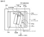
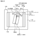
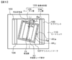
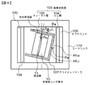
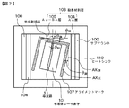
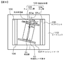
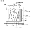
上記の目的を達成するための本発明のサブマウントは、光入出射端面の法線に対して軸線がθWG(度)傾き、屈折率nLEを有する半導体材料から成る導波路を備えた半導体発光素子を固定するためのサブマウントであって、
半導体発光素子を取り付ける第1面には、半導体発光素子を固定するための融着材料層が設けられており、
半導体発光素子の光入出射端面の外側近傍の光通過媒質の屈折率をn0としたとき、角度θSM=sin-1[nLE・sin(θWG)/n0]を識別できるアライメントマークが、融着材料層に形成されている。
In order to achieve the above object, a submount of the present invention is a semiconductor including a waveguide made of a semiconductor material having an axis tilted by θ WG (degrees) with respect to the normal of the light incident / exit end face and a refractive index n LE A submount for fixing the light emitting element,
The first surface to which the semiconductor light emitting element is attached is provided with a fusion material layer for fixing the semiconductor light emitting element.
An alignment mark that can identify the angle θ SM = sin −1 [n LE · sin (θ WG ) / n 0 ], where n 0 is the refractive index of the light passing medium near the outside of the light incident / exit end face of the semiconductor light emitting device. Is formed in the fusion material layer.
上記の目的を達成するための本発明の第1の態様に係るサブマウント組立体は、
光入出射端面の法線に対して軸線がθWG(度)傾き、屈折率nLEを有する半導体材料から成る導波路を備えた半導体発光素子、及び、
半導体発光素子を固定するためのサブマウント、
を具備したサブマウント組立体であって、
サブマウントの半導体発光素子を取り付ける第1面には、半導体発光素子を固定するための融着材料層が設けられており、
半導体発光素子の光入出射端面の外側近傍の光通過媒質の屈折率をn0としたとき、角度θSM=sin-1[nLE・sin(θWG)/n0]を識別できるアライメントマークが、融着材料層に形成されている。
In order to achieve the above object, a submount assembly according to the first aspect of the present invention comprises:
A semiconductor light emitting device including a waveguide made of a semiconductor material having an axis inclined by θ WG (degrees) with respect to the normal of the light incident / exit end face, and a refractive index n LE ;
A submount for fixing a semiconductor light emitting device,
A submount assembly comprising:
On the first surface to which the semiconductor light emitting element of the submount is attached, a fusion material layer for fixing the semiconductor light emitting element is provided,
An alignment mark that can identify the angle θ SM = sin −1 [n LE · sin (θ WG ) / n 0 ], where n 0 is the refractive index of the light passing medium near the outside of the light incident / exit end face of the semiconductor light emitting device. Is formed in the fusion material layer.
上記の目的を達成するための本発明の第2の態様に係るサブマウント組立体は、
光入出射端面の法線に対して軸線がθWG(度)傾き、屈折率nLEを有する半導体材料から成る導波路を備えた半導体発光素子を固定するためのサブマウント、及び、
サブマウントを取り付けるためのヒートシンク、
を具備したサブマウント組立体であって、
サブマウントの半導体発光素子を取り付ける第1面には、半導体発光素子を固定するための融着材料層が設けられており、
サブマウントの第1面と対向する第2面には、接着層が形成されており、
サブマウントは接着層を介してヒートシンクに取り付けられており、
半導体発光素子の光入出射端面の外側近傍の光通過媒質の屈折率をn0としたとき、角度θSM=sin-1[nLE・sin(θWG)/n0]を識別できるアライメントマークが、融着材料層に形成されている。
In order to achieve the above object, a submount assembly according to the second aspect of the present invention comprises:
A submount for fixing a semiconductor light emitting device having a waveguide made of a semiconductor material having an axis inclined by θ WG (degrees) relative to the normal line of the light incident / exit end face and a refractive index n LE ;
Heat sink for mounting submount,
A submount assembly comprising:
On the first surface to which the semiconductor light emitting element of the submount is attached, a fusion material layer for fixing the semiconductor light emitting element is provided,
An adhesive layer is formed on the second surface facing the first surface of the submount,
The submount is attached to the heat sink via an adhesive layer,
An alignment mark that can identify the angle θ SM = sin −1 [n LE · sin (θ WG ) / n 0 ], where n 0 is the refractive index of the light passing medium near the outside of the light incident / exit end face of the semiconductor light emitting device. Is formed in the fusion material layer.
上記の目的を達成するための本発明の第1の態様に係るサブマウント組立方法は、
光入出射端面の法線に対して軸線がθWG(度)傾き、屈折率nLEを有する半導体材料から成る導波路を備えた半導体発光素子、及び、
半導体発光素子を固定するためのサブマウント、
を具備し、
サブマウントの半導体発光素子を取り付ける第1面には、半導体発光素子を固定するための融着材料層が設けられており、
半導体発光素子の光入出射端面の外側近傍の光通過媒質の屈折率をn0としたとき、角度θSM=sin-1[nLE・sin(θWG)/n0]を識別できるアライメントマークが、融着材料層に形成されたサブマウント組立体の組立方法であって、
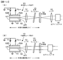
アライメントマークを基準として、サブマウントと半導体発光素子とを位置合わせした後、融着材料層を溶融・冷却させて、サブマウントに半導体発光素子を取り付ける。
In order to achieve the above object, a submount assembling method according to the first aspect of the present invention comprises:
A semiconductor light emitting device including a waveguide made of a semiconductor material having an axis inclined by θ WG (degrees) with respect to the normal of the light incident / exit end face, and a refractive index n LE ;
A submount for fixing a semiconductor light emitting device,
Comprising
On the first surface to which the semiconductor light emitting element of the submount is attached, a fusion material layer for fixing the semiconductor light emitting element is provided,
An alignment mark that can identify the angle θ SM = sin −1 [n LE · sin (θ WG ) / n 0 ], where n 0 is the refractive index of the light passing medium near the outside of the light incident / exit end face of the semiconductor light emitting device. Is a method of assembling the submount assembly formed in the fusion material layer,
After aligning the submount and the semiconductor light emitting element with the alignment mark as a reference, the fusion material layer is melted and cooled, and the semiconductor light emitting element is attached to the submount.
上記の目的を達成するための本発明の第2の態様に係るサブマウント組立方法は、
光入出射端面の法線に対して軸線がθWG(度)傾き、屈折率nLEを有する半導体材料から成る導波路を備えた半導体発光素子を固定するためのサブマウント、及び、
サブマウントを取り付けるためのヒートシンク、
を具備し、
サブマウントの半導体発光素子を取り付ける第1面には、半導体発光素子を固定するための融着材料層が設けられており、
半導体発光素子の光入出射端面の外側近傍の光通過媒質の屈折率をn0としたとき、角度θSM=sin-1[nLE・sin(θWG)/n0]を識別できるアライメントマークが、融着材料層に形成されたサブマウント組立体の組立方法であって、
アライメントマークを基準として、サブマウントとヒートシンクとを位置合わせした後、接着層を溶融・冷却させて、サブマウントをヒートシンクに取り付ける。
In order to achieve the above object, a submount assembling method according to the second aspect of the present invention comprises:
A submount for fixing a semiconductor light emitting device having a waveguide made of a semiconductor material having an axis inclined by θ WG (degrees) relative to the normal line of the light incident / exit end face and a refractive index n LE ;
Heat sink for mounting submount,
Comprising
On the first surface to which the semiconductor light emitting element of the submount is attached, a fusion material layer for fixing the semiconductor light emitting element is provided,
An alignment mark that can identify the angle θ SM = sin −1 [n LE · sin (θ WG ) / n 0 ], where n 0 is the refractive index of the light passing medium near the outside of the light incident / exit end face of the semiconductor light emitting device. Is a method of assembling the submount assembly formed in the fusion material layer,
After aligning the submount and the heat sink with the alignment mark as a reference, the adhesive layer is melted and cooled to attach the submount to the heat sink.
本発明の第1の態様に係るサブマウント組立方法と本発明の第2の態様に係るサブマウント組立方法とを組み合わせることができ、この場合、本発明の第1の態様に係るサブマウント組立方法を行い、次いで、本発明の第2の態様に係るサブマウント組立方法を後に行ってもよいし、本発明の第2の態様に係るサブマウント組立方法を行い、次いで、本発明の第1の態様に係るサブマウント組立方法を行ってもよい。あるいは又、本発明の第1の態様に係るサブマウント組立方法と本発明の第2の態様に係るサブマウント組立方法とを同時に行ってもよい。 The submount assembling method according to the first aspect of the present invention and the submount assembling method according to the second aspect of the present invention can be combined. In this case, the submount assembling method according to the first aspect of the present invention is combined. Then, the submount assembling method according to the second aspect of the present invention may be performed later, or the submount assembling method according to the second aspect of the present invention is performed, and then the first of the present invention You may perform the submount assembly method which concerns on an aspect. Alternatively, the submount assembling method according to the first aspect of the present invention and the submount assembling method according to the second aspect of the present invention may be performed simultaneously.
本発明のサブマウント、サブマウント組立体、サブマウント組立体の組立方法にあっては、角度θSM=sin-1[nLE・sin(θWG)/n0]を識別できるアライメントマークが、融着材料層に形成されている。それ故、斜め導波路を有する半導体発光素子において、組立コストが増加したり、歩留りや信頼性の低下といった問題が生じ難い。しかも、斜め導波路を有する半導体発光素子を従来のシステムに容易に組み込むことができるし、半導体発光素子の光結合効率を向上させることができ、システム全体の性能が向上する。また、現状の半導体発光素子やサブマウントの作製プロセスを大幅に変更する必要がないし、画像認識装置を用いて実装できるため、作製コスト、ランニングコストの大幅な低減が可能となる。 In the submount, the submount assembly, and the method of assembling the submount assembly of the present invention, an alignment mark that can identify the angle θ SM = sin −1 [n LE · sin (θ WG ) / n 0 ] It is formed in the fusion material layer. Therefore, in a semiconductor light emitting device having an oblique waveguide, problems such as an increase in assembly cost and a decrease in yield and reliability are unlikely to occur. In addition, a semiconductor light emitting device having an oblique waveguide can be easily incorporated into a conventional system, the optical coupling efficiency of the semiconductor light emitting device can be improved, and the performance of the entire system is improved. In addition, it is not necessary to significantly change the manufacturing process of the current semiconductor light emitting element and submount, and mounting can be performed using an image recognition device, so that manufacturing cost and running cost can be significantly reduced.
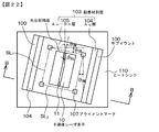
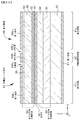
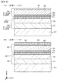
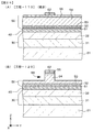
以下、図面を参照して、実施例に基づき本発明を説明するが、本発明は実施例に限定されるものではなく、実施例における種々の数値や材料は例示である。尚、説明は、以下の順序で行う。
1.本発明のサブマウント、本発明の第1の態様及び第2の態様に係るサブマウント組立体、並びに、本発明の第1の態様及び第2の態様に係るサブマウント組立方法、全般に関する説明
2.実施例1(本発明のサブマウント、本発明の第1の態様に係るサブマウント組立体、並びに、本発明の第1の態様に係るサブマウント組立方法)
3.実施例2(実施例1の変形)
4.実施例3(実施例2の変形)
5.実施例4(本発明のサブマウント、本発明の第2の態様に係るサブマウント組立体、並びに、本発明の第2の態様に係るサブマウント組立方法)、その他
Hereinafter, the present invention will be described based on examples with reference to the drawings. However, the present invention is not limited to the examples, and various numerical values and materials in the examples are examples. The description will be given in the following order.
1. Submount of the present invention, submount assembly according to the first and second aspects of the present invention, and submount assembling method according to the first and second aspects of the present invention,
3. Example 2 (Modification of Example 1)
4). Example 3 (Modification of Example 2)
5. Example 4 (submount of the present invention, submount assembly according to the second aspect of the present invention, and submount assembling method according to the second aspect of the present invention), etc.
本発明の第1の態様に係るサブマウント組立体にあっては、サブマウントを取り付けるためのヒートシンクを更に具備している形態とすることができる。 The submount assembly according to the first aspect of the present invention may further include a heat sink for attaching the submount.
本発明のサブマウント、上記の好ましい形態を含む本発明の第1の態様及び第2の態様に係るサブマウント組立体、並びに、本発明の第1の態様及び第2の態様に係るサブマウント組立方法において、半導体発光素子は、半導体レーザ素子から成る構成とすることができるし、あるいは又、半導体光増幅器(半導体レーザ増幅器,SOA)から成る構成とすることができる。 The submount of the present invention, the submount assembly according to the first and second aspects of the present invention including the above preferred embodiments, and the submount assembly according to the first and second aspects of the present invention In the method, the semiconductor light emitting element can be constituted by a semiconductor laser element, or can be constituted by a semiconductor optical amplifier (semiconductor laser amplifier, SOA).
上記の好ましい形態、構成を含む本発明のサブマウント、本発明の第1の態様及び第2の態様に係るサブマウント組立体、並びに、本発明の第1の態様及び第2の態様に係るサブマウント組立方法において、半導体発光素子をサブマウントに取り付けたとき、サブマウントの軸線と半導体発光素子の軸線とはθSM(度)を成して交わる構成とすることができる。そして、このような構成において、融着材料層には、少なくとも2つの点状のアライメントマークが設けられており、2つのアライメントマークを結ぶ直線は、サブマウントの軸線とθSM(度)又は(90−θSM)(度)を成して交わっている形態とすることができ、あるいは又、融着材料層には、少なくとも1つの帯状のアライメントマークが設けられており、アライメントマークの軸線は、サブマウントの軸線とθSM(度)又は(90−θSM)(度)を成して交わっている形態とすることができる。 The submount of the present invention including the above preferred embodiments and configurations, the submount assembly according to the first and second aspects of the present invention, and the submount according to the first and second aspects of the present invention. In the mount assembly method, when the semiconductor light emitting element is attached to the submount, the axis of the submount and the axis of the semiconductor light emitting element intersect each other at θ SM (degrees). In such a configuration, the fusion material layer is provided with at least two dot-like alignment marks, and the straight line connecting the two alignment marks is the submount axis and θ SM (degrees) or ( 90-θ SM ) (degrees), or the fusion material layer is provided with at least one strip-shaped alignment mark, and the axis of the alignment mark is The axis of the submount and θ SM (degrees) or (90−θ SM ) (degrees) may be crossed.
あるいは又、上記の好ましい形態、構成を含む本発明のサブマウント、本発明の第1の態様及び第2の態様に係るサブマウント組立体、並びに、本発明の第1の態様及び第2の態様に係るサブマウント組立方法において、第1面と対向する第2面には、接着層が形成されており、サブマウントは接着層を介してヒートシンクに取り付けられ、サブマウントをヒートシンクに取り付けたとき、サブマウントの軸線とヒートシンクの軸線とはθSM(度)を成して交わる構成とすることができる。そして、このような構成において、融着材料層には、少なくとも2つの点状のアライメントマークが設けられており、2つのアライメントマークを結ぶ直線は、サブマウントの軸線とθSM(度)又は(90−θSM)(度)を成して交わっている形態とすることができ、あるいは又、融着材料層には、少なくとも1つの帯状のアライメントマークが設けられており、アライメントマークの軸線は、サブマウントの軸線とθSM(度)又は(90−θSM)(度)を成して交わっている形態とすることができる。 Alternatively, the submount of the present invention including the above-mentioned preferred forms and configurations, the submount assembly according to the first and second aspects of the present invention, and the first and second aspects of the present invention. In the submount assembling method according to the present invention, an adhesive layer is formed on the second surface opposite to the first surface, the submount is attached to the heat sink via the adhesive layer, and when the submount is attached to the heat sink, The axis of the submount and the axis of the heat sink can be configured to intersect at θ SM (degrees). In such a configuration, the fusion material layer is provided with at least two dot-like alignment marks, and the straight line connecting the two alignment marks is the submount axis and θ SM (degrees) or ( 90-θ SM ) (degrees), or the fusion material layer is provided with at least one strip-shaped alignment mark, and the axis of the alignment mark is The axis of the submount and θ SM (degrees) or (90−θ SM ) (degrees) may be crossed.
融着材料層に2つの点状のアライメントマークを設ける場合、2つのアライメントマークを結ぶ直線がサブマウントの軸線とθSM(度)を成して交わるように2つのアライメントマークを配置してもよいし、2つのアライメントマークを結ぶ直線がサブマウントの軸線と(90−θSM)(度)を成して交わるように2つのアライメントマークを配置してもよい。また、融着材料層に3つの点状のアライメントマークを設ける場合、第1のアライメントマークと第2のアライメントマークを結ぶ直線がサブマウントの軸線とθSM(度)を成して交わり、第2のアライメントマークと第3のアライメントマークを結ぶ直線がサブマウントの軸線と(90−θSM)(度)を成して交わるように、3つのアライメントマークを配置すればよい。更には、融着材料層に4つの点状のアライメントマークを設ける場合、第1のアライメントマークと第2のアライメントマーク、第3のアライメントマークと第4のアライメントマークを結ぶ直線がサブマウントの軸線とθSM(度)を成して交わり、第1のアライメントマークと第4のアライメントマーク、第2のアライメントマークと第3のアライメントマークを結ぶ直線がサブマウントの軸線と(90−θSM)(度)を成して交わるように、4つのアライメントマークを配置すればよい。 When two dot-shaped alignment marks are provided on the fusion material layer, the two alignment marks may be arranged so that the straight line connecting the two alignment marks intersects the axis of the submount at θ SM (degrees). Alternatively, the two alignment marks may be arranged so that a straight line connecting the two alignment marks intersects the axis of the submount and forms (90−θ SM ) (degrees). Further, when three dot alignment marks are provided on the fusion material layer, the straight line connecting the first alignment mark and the second alignment mark intersects with the axis of the submount to form θ SM (degrees), The three alignment marks may be arranged so that the straight line connecting the second alignment mark and the third alignment mark intersects with the axis of the submount at (90−θ SM ) (degrees). Further, when four dot-shaped alignment marks are provided on the fusion material layer, the straight line connecting the first alignment mark and the second alignment mark, and the third alignment mark and the fourth alignment mark is the axis of the submount. And θ SM (degrees) intersect, and the straight line connecting the first alignment mark and the fourth alignment mark, and the second alignment mark and the third alignment mark is the axis of the submount (90−θ SM ) Four alignment marks may be arranged so as to intersect with each other.
融着材料層に1つの帯状のアライメントマークを設ける場合、アライメントマークの軸線が、サブマウントの軸線とθSM(度)を成して交わるように1つの帯状のアライメントマークを配置してもよいし、アライメントマークの軸線が、サブマウントの軸線と(90−θSM)(度)を成して交わるように1つの帯状のアライメントマークを配置してもよい。融着材料層に2つの帯状のアライメントマークを設ける場合、2つの帯状のアライメントマークの軸線が、サブマウントの軸線とθSM(度)を成して交わるように2つの帯状のアライメントマークを配置してもよいし、2つの帯状のアライメントマークの軸線が、サブマウントの軸線と(90−θSM)(度)を成して交わるように2つの帯状のアライメントマークを配置してもよいし、一方の帯状のアライメントマークの軸線がサブマウントの軸線とθSM(度)を成して交わり、他方の帯状のアライメントマークの軸線がサブマウントの軸線と(90−θSM)(度)を成して交わるように、2つの帯状のアライメントマークを配置してもよい。融着材料層に3つの帯状のアライメントマークを設ける場合、2つの帯状のアライメントマークの軸線が、サブマウントの軸線とθSM(度)を成して交わるように2つの帯状のアライメントマークを配置し、残りの1つの帯状のアライメントマークの軸線が、サブマウントの軸線と(90−θSM)(度)を成して交わるように、3つの帯状のアライメントマークを配置してもよいし、2つの帯状のアライメントマークの軸線が、サブマウントの軸線と(90−θSM)(度)を成して交わるように2つの帯状のアライメントマークを配置し、残りの1つの帯状のアライメントマークの軸線が、サブマウントの軸線とθSM(度)を成して交わるように、3つの帯状のアライメントマークを配置してもよい。融着材料層に4つの帯状のアライメントマークを設ける場合、第1の帯状のアライメントマーク及び第3の帯状のアライメントマークの軸線が、サブマウントの軸線とθSM(度)を成して交わり、第2の帯状のアライメントマーク及び第4の帯状のアライメントマークの軸線が、サブマウントの軸線と(90−θSM)(度)を成して交わるように、4つの帯状のアライメントマークを配置すればよい。 When providing one band-shaped alignment mark in the fusion material layer, one band-shaped alignment mark may be arranged so that the axis of the alignment mark intersects with the axis of the submount at θ SM (degrees). One alignment mark may be arranged so that the axis of the alignment mark intersects the axis of the submount so as to form (90−θ SM ) (degrees). When two belt-shaped alignment marks are provided on the fusion material layer, the two belt-shaped alignment marks are arranged so that the axis of the two belt-shaped alignment marks intersects the axis of the submount at θ SM (degrees). Alternatively, the two belt-like alignment marks may be arranged so that the axes of the two belt-like alignment marks intersect with the submount axis at (90−θ SM ) (degrees). The axis of one band-shaped alignment mark intersects the axis of the submount with θ SM (degrees), and the axis of the other band-shaped alignment mark intersects with the axis of the submount (90−θ SM ) (degrees). Two belt-shaped alignment marks may be arranged so as to cross each other. When three belt-like alignment marks are provided on the fusion material layer, the two belt-like alignment marks are arranged so that the axis of the two belt-like alignment marks intersects the axis of the submount at θ SM (degrees). The three belt-like alignment marks may be arranged so that the axis of the remaining one belt-like alignment mark intersects with the axis of the submount at (90−θ SM ) (degrees). Two belt-like alignment marks are arranged so that the axis of the two belt-like alignment marks intersects the axis of the submount so as to form (90-θ SM ) (degrees), and the remaining one of the belt-like alignment marks Three belt-shaped alignment marks may be arranged so that the axis intersects the axis of the submount at θ SM (degrees). When four belt-shaped alignment marks are provided on the fusion material layer, the axes of the first belt-shaped alignment mark and the third belt-shaped alignment mark intersect with the axis of the submount to form θ SM (degrees), The four belt-like alignment marks are arranged so that the axes of the second belt-like alignment mark and the fourth belt-like alignment mark intersect with the submount axis at (90-θ SM ) (degrees). That's fine.
以上に説明した各種の好ましい形態、構成を含む本発明のサブマウント、本発明の第1の態様及び第2の態様に係るサブマウント組立体、並びに、本発明の第1の態様及び第2の態様に係るサブマウント組立方法において、融着材料層は、第1面側から、Au層、及び、Au−Sn合金層(例えば、Au80Sn20合金層)の積層構造を有し、アライメントマークは、Au−Sn合金層に設けられた開口部から成り、開口部の底部にAu層が露出している構成とすることができる。このような構成とすることで、画像認識装置によってアライメントマークを容易に検出することができる。但し、融着材料層はこのような構成に限定するものではなく、融着材料層は、第1面側から、Au層、及び、Ag−Sn合金層の積層構造を有していてもよい。そして、このような2層構成の融着材料層にあっては、Au−Sn合金層の射影像はAu層の射影像に含まれる形態とすることが好ましく、これによって、例えば、Au層にボンディング法に基づき配線等を接続することができる。但し、融着材料層は、このような材料構成、層構成に限定されるものではない。融着材料層を構成する材料として、あるいは又、接着層を構成する材料として、所謂低融点金属(合金)材料や半田材料、ロウ材を用いることができ、例えば、In(インジウム:融点157゜C);インジウム−金系の低融点合金;Sn80Ag20(融点220〜370゜C)、Sn95Cu5(融点227〜370゜C)等の錫(Sn)系高温はんだ;Pb97.5Ag2.5(融点304゜C)、Pb94.5Ag5.5(融点304〜365゜C)、Pb97.5Ag1.5Sn1.0(融点309゜C)等の鉛(Pb)系高温はんだ;Zn95Al5(融点380゜C)等の亜鉛(Zn)系高温はんだ;Sn5Pb95(融点300〜314゜C)、Sn2Pb98(融点316〜322゜C)等の錫−鉛系標準はんだ;Au88Ga12(融点381゜C)等のろう材(以上の添字は全て原子%を表す)を例示することができる。尚、半導体発光素子とサブマウントを加熱して接合し、ヒートシンクとサブマウントを加熱して接合する場合、先の工程で加熱する融着材料層あるいは接着層を構成する材料の融点よりも、後の工程で加熱する接着層あるいは融着材料層を構成する材料の融点が低いことが必要とされる。半導体発光素子とサブマウントとヒートシンクとサブマウントを加熱して同時に接合する場合には、融着材料層と接着層を構成する材料として、同じ材料を用いることができる。融着材料層や接着層は、例えば、真空蒸着法やスパッタリング法等のPVD法にて成膜することができるし、アライメントマークは、例えば、エッチング法やリフトオフ法に基づき形成することができる。
The submount of the present invention including the various preferred embodiments and configurations described above, the submount assembly according to the first and second aspects of the present invention, and the first and second aspects of the present invention. In the submount assembling method according to the aspect, the fusion material layer has a laminated structure of an Au layer and an Au—Sn alloy layer (for example, Au 80 Sn 20 alloy layer) from the first surface side, and an alignment mark Can consist of an opening provided in the Au—Sn alloy layer, and the Au layer is exposed at the bottom of the opening. With such a configuration, the alignment mark can be easily detected by the image recognition apparatus. However, the fusion material layer is not limited to such a configuration, and the fusion material layer may have a laminated structure of an Au layer and an Ag—Sn alloy layer from the first surface side. . And in such a two-layered fusion material layer, it is preferable that the projected image of the Au—Sn alloy layer is included in the projected image of the Au layer. Wiring and the like can be connected based on the bonding method. However, the fusion material layer is not limited to such a material configuration and layer configuration. A so-called low melting point metal (alloy) material, a solder material, or a brazing material can be used as the material constituting the fusing material layer or the material constituting the adhesive layer. For example, In (indium: melting point 157 °). C); Indium-gold low melting point alloy; Sn 80 Ag 20 (melting point 220 to 370 ° C.), Sn 95 Cu 5 (melting point 227 to 370 ° C.) or other tin (Sn) high temperature solder; Pb 97.5 Ag Lead (Pb) -based high-temperature solder such as 2.5 (melting point 304 ° C.), Pb 94.5 Ag 5.5 (melting point 304 to 365 ° C.), Pb 97.5 Ag 1.5 Sn 1.0 (melting point 309 ° C.); Zn 95 Al 5 (melting point 380 ° C) zinc (Zn) -based high-temperature solder; Sn 5 Pb 95 (
サブマウントを構成する材料として、AlN、ダイアモンド、Si、SiCを例示することができるし、ヒートシンクを構成する材料として、銅、銅タングステン、銅合金、鉄、ステンレス鋼、アルミニウム、アルミニウム合金、タングステン、モリブデン、銅モリブデン、アルミニウム・シリコンカーバイトを例示することができる。サブマウントやヒートシンクは周知の方法で作製すればよい。 Examples of the material constituting the submount include AlN, diamond, Si, and SiC, and examples of the material constituting the heat sink include copper, copper tungsten, copper alloy, iron, stainless steel, aluminum, aluminum alloy, tungsten, Examples include molybdenum, copper molybdenum, and aluminum / silicon carbide. What is necessary is just to produce a submount and a heat sink by a well-known method.
更には、以上に説明した各種の好ましい形態、構成を含む本発明のサブマウント、本発明の第1の態様及び第2の態様に係るサブマウント組立体、並びに、本発明の第1の態様及び第2の態様に係るサブマウント組立方法において、アライメントマークは半導体発光素子と重なり得る形態とすることができるし、あるいは又、アライメントマークは半導体発光素子と重ならない形態とすることができる。前者の場合、半導体発光素子の上方から、半導体発光素子を通してアライメントマークが識別できるような材料から(例えば、GaN系化合物半導体)から半導体発光素子を構成すればよいし、あるいは又、アライメントマークの上方に位置する半導体発光素子の構成要素を透明な材料から構成すればよい。 Furthermore, the submount of the present invention including the various preferred embodiments and configurations described above, the submount assembly according to the first and second aspects of the present invention, and the first aspect of the present invention and In the submount assembling method according to the second aspect, the alignment mark can be configured to overlap with the semiconductor light emitting element, or the alignment mark can be configured not to overlap with the semiconductor light emitting element. In the former case, the semiconductor light emitting device may be formed from a material (for example, GaN-based compound semiconductor) from which the alignment mark can be identified through the semiconductor light emitting device, or from above the semiconductor light emitting device. What is necessary is just to comprise the component of the semiconductor light-emitting device located in a transparent material.
半導体発光素子をサブマウントに取り付けるには、後述する第2電極をサブマウントに取り付けてもよいし、後述する第1電極をサブマウントに取り付けてもよい。前者の場合、サブマウントの上に、化合物半導体層、基板がこの順に積層された構造となり、所謂ジャンクション・ダウン方式での半導体発光素子の取り付けとなる。一方、後者の場合、サブマウントの上に、基板、化合物半導体層がこの順に積層された構造となり、所謂ジャンクション・アップ方式での半導体発光素子の取り付けとなる。 In order to attach the semiconductor light emitting element to the submount, a second electrode described later may be attached to the submount, or a first electrode described later may be attached to the submount. In the former case, a compound semiconductor layer and a substrate are stacked in this order on the submount, and the semiconductor light emitting device is attached by a so-called junction down method. On the other hand, in the latter case, the substrate and the compound semiconductor layer are stacked in this order on the submount, and the semiconductor light emitting device is attached by a so-called junction-up method.
更には、以上に説明した各種の好ましい形態、構成を含む本発明のサブマウント、本発明の第1の態様及び第2の態様に係るサブマウント組立体、並びに、本発明の第1の態様及び第2の態様に係るサブマウント組立方法において、半導体発光素子の光入出射端面は、サブマウントから突出し得る形態とすることができ、これによって、所謂ジャンクション・ダウン方式での半導体発光素子の取り付けを行うことができ、ヒートシンクによる半導体発光素子の冷却効果を一層向上させることができる。 Furthermore, the submount of the present invention including the various preferred embodiments and configurations described above, the submount assembly according to the first and second aspects of the present invention, and the first aspect of the present invention and In the submount assembling method according to the second aspect, the light incident / exit end face of the semiconductor light emitting element can be protruded from the submount, and thereby mounting the semiconductor light emitting element in a so-called junction down system. The cooling effect of the semiconductor light emitting element by the heat sink can be further improved.
角度θWGとして、0.1度≦θWG≦10度、好ましくは、2度≦θWG≦6度を例示することができる。導波路の軸線とは、例えば、半導体発光素子がリッジストライプ構造を有する場合、リッジストライプ構造の幅方向に沿った両側面を結ぶ線分の二等分点を結ぶ直線あるいは線分の組合せである。また、光入出射端面の法線に対して軸線がθWG(度)傾いているが、半導体発光素子の構成、構造に依存して、光入射端面の法線に対して軸線がθWG(度)傾いている場合もあるし、光出射端面の法線に対して軸線がθWG(度)傾いている婆もあるし、2つの光入出射端面の法線に対して軸線がθWG(度)傾いている場合もある。 Examples of the angle θ WG include 0.1 degrees ≦ θ WG ≦ 10 degrees, preferably 2 degrees ≦ θ WG ≦ 6 degrees. For example, when the semiconductor light emitting device has a ridge stripe structure, the axis of the waveguide is a straight line or a combination of line segments connecting bisectors of line segments connecting both side surfaces along the width direction of the ridge stripe structure. . In addition, although the axis is inclined by θ WG (degrees) with respect to the normal line of the light incident / exit end face, depending on the configuration and structure of the semiconductor light emitting device, the axis line is θ WG ( it some cases even the tilted degrees), to some Baba axis is inclined theta WG (degrees) with respect to a normal to the light emitting end face, the axis with respect to the two normals of the light input and output end faces theta WG (Degree) may be inclined.
以上に説明した各種の好ましい形態、構成を含む本発明のサブマウント、本発明の第1の態様及び第2の態様に係るサブマウント組立体、並びに、本発明の第1の態様及び第2の態様に係るサブマウント組立方法(以下、これらを総称して、単に『本発明』と呼ぶ)において、半導体発光素子を半導体レーザ素子から構成する場合、周知の連続発振型の半導体レーザ素子とすることもできるし、パルス発振型の半導体レーザ素子とすることもできる。後者の場合、例えば、モード同期半導体レーザ素子を構成する半導体レーザ素子として、発光領域及び可飽和吸収領域を設けた半導体レーザ素子を挙げることができ、具体的には、発光領域及び可飽和吸収領域の配置状態から、半導体レーザ素子は、発光領域と可飽和吸収領域とを垂直方向に配置したSAL(Saturable Absorber Layer)型やWI(Weakly Index guide)型と、共振器(導波路)方向に発光領域と可飽和吸収領域とを並置した多電極型(Multi Section)型とに分類することができる。 The submount of the present invention including the various preferred embodiments and configurations described above, the submount assembly according to the first and second aspects of the present invention, and the first and second aspects of the present invention. In the submount assembling method according to the aspect (hereinafter collectively referred to simply as “the present invention”), when the semiconductor light emitting element is constituted by a semiconductor laser element, a known continuous oscillation type semiconductor laser element is used. Alternatively, a pulse oscillation type semiconductor laser element can be formed. In the latter case, for example, the semiconductor laser element constituting the mode-locked semiconductor laser element can include a semiconductor laser element provided with a light emitting region and a saturable absorption region. Specifically, the light emitting region and the saturable absorption region can be exemplified. Therefore, the semiconductor laser device emits light in the cavity (waveguide) direction and the SAL (Saturable Absorber Layer) type and WI (Weakly Index guide) type in which the light emitting region and the saturable absorption region are arranged vertically. It can be classified into a multi-electrode type in which the region and the saturable absorption region are juxtaposed.
ここで、多電極型半導体レーザ素子の一形態は、
(a)第1導電型を有し、GaN系化合物半導体から成る第1化合物半導体層、GaN系化合物半導体から成る発光領域及び可飽和吸収領域を構成する第3化合物半導体層(活性層)、並びに、第1導電型と異なる第2導電型を有し、GaN系化合物半導体から成る第2化合物半導体層が、順次、積層されて成る積層構造体、
(b)第2化合物半導体層上に形成された第2電極、並びに、
(c)第1化合物半導体層に電気的に接続された第1電極、
を備え、
第2電極は、発光領域を経由して第1電極に電流を流すことで順バイアス状態とするための第1部分と、可飽和吸収領域に電界を加えるための第2部分とに、分離溝によって分離されている、バイ・セクション型の形態とすることができる。尚、このような構成を有する半導体レーザ素子を、便宜上、『本発明における半導体レーザ素子』と呼ぶ場合がある。
Here, one form of the multi-electrode semiconductor laser element is:
(A) a first compound semiconductor layer having a first conductivity type and made of a GaN compound semiconductor, a third compound semiconductor layer (active layer) constituting a light emitting region and a saturable absorption region made of a GaN compound semiconductor, and A stacked structure in which second compound semiconductor layers having a second conductivity type different from the first conductivity type and made of a GaN-based compound semiconductor are sequentially stacked;
(B) a second electrode formed on the second compound semiconductor layer, and
(C) a first electrode electrically connected to the first compound semiconductor layer;
With
The second electrode has a separation groove formed between a first portion for making a forward bias state by passing a current through the first electrode through the light emitting region and a second portion for applying an electric field to the saturable absorption region. Can be in the form of a bi-section type, separated by The semiconductor laser element having such a configuration may be referred to as “semiconductor laser element in the present invention” for convenience.
そして、第2電極の第1部分と第2部分との間の電気抵抗値は、第2電極と第1電極との間の電気抵抗値の1×10倍以上、好ましくは1×10²倍以上、より好ましくは1×10³倍以上であることが望ましい。尚、このような本発明における半導体レーザ素子を、便宜上、『第1の構成の半導体レーザ素子』と呼ぶ。あるいは又、第2電極の第1部分と第2部分との間の電気抵抗値は、1×10²Ω以上、好ましくは1×10³Ω以上、より好ましくは1×10⁴Ω以上であることが望ましい。尚、このような本発明における半導体レーザ素子を、便宜上、『第2の構成の半導体レーザ素子』と呼ぶ。 The electrical resistance value between the first part and the second part of the second electrode is 1 × 10 times or more, preferably 1 × 10 2 times the electrical resistance value between the second electrode and the first electrode. As described above, it is desirable that the ratio is 1 × 10 3 times or more. Such a semiconductor laser device according to the present invention is referred to as “semiconductor laser device having the first configuration” for convenience. Alternatively, the electrical resistance value between the first portion and the second portion of the second electrode is 1 × 10 2 Ω or more, preferably 1 × 10 3 Ω or more, more preferably 1 × 10 4 Ω or more. It is desirable. Note that such a semiconductor laser element according to the present invention is referred to as a “second configuration semiconductor laser element” for convenience.
このような第1の構成あるいは第2の構成の半導体レーザ素子にあっては、第2電極の第1部分と第2部分との間の電気抵抗値は、第2電極と第1電極との間の電気抵抗値の10倍以上であり、あるいは又、1×10²Ω以上である。従って、第2電極の第1部分から第2部分への漏れ電流の流れを確実に抑制することができる。即ち、発光領域(キャリア注入領域、利得領域)に注入する電流を大きくできると同時に、可飽和吸収領域(キャリア非注入領域)へ印加する逆バイアス電圧Vsaを高くすることができるため、時間的に短いレーザ光を有するシングルモードのモード同期動作を実現できる。そして、第2電極の第1部分と第2部分との間のこのような高い電気抵抗値を、第2電極を第1部分と第2部分とに分離溝によって分離するだけで達成することができる。 In the semiconductor laser device having such a first configuration or the second configuration, the electrical resistance value between the first portion and the second portion of the second electrode is between the second electrode and the first electrode. The electrical resistance value between them is 10 times or more, or 1 × 10 2 Ω or more. Therefore, the leakage current flow from the first part to the second part of the second electrode can be reliably suppressed. That is, since the current injected into the light emitting region (carrier injection region, gain region) can be increased, the reverse bias voltage V sa applied to the saturable absorption region (carrier non-injection region) can be increased. It is possible to realize a single-mode mode synchronization operation with a short laser beam. And, such a high electrical resistance value between the first part and the second part of the second electrode can be achieved simply by separating the second electrode into the first part and the second part by the separation groove. it can.
第1の構成あるいは第2の構成の半導体レーザ素子にあっては、第2電極の第1部分から発光領域を経由して第1電極に電流を流して順バイアス状態とし、第1電極と第2電極の第2部分との間に電圧を印加することによって可飽和吸収領域に電界を加えることで、モード同期動作させることができる。また、第1電極と第2部分との間には、逆バイアス電圧を印加する構成(即ち、第1電極を正極、第2部分を負極とする構成)とすることが望ましい。尚、第2電極の第2部分には、第2電極の第1部分に印加するパルス電流あるいはパルス電圧と同期したパルス電流あるいはパルス電圧を印加してもよいし、直流バイアスを印加してもよい。また、第2電極から発光領域を経由して第1電極に電流を流し、且つ、第2電極から発光領域を経由して第1電極に外部電気信号を重畳させる形態とすることができる。そして、これによって、光パルスと外部電気信号との間の同期を取ることができる。あるいは又、積層構造体の光入射端面から光信号を入射させる形態とすることができる。そして、これによっても、光パルスと光信号との間の同期を取ることができる。 In the semiconductor laser device having the first configuration or the second configuration, a current is caused to flow from the first portion of the second electrode to the first electrode via the light emitting region so as to be in a forward bias state. A mode-locked operation can be performed by applying an electric field to the saturable absorption region by applying a voltage between the second part of the two electrodes. Further, it is desirable that a reverse bias voltage be applied between the first electrode and the second portion (that is, a configuration in which the first electrode is a positive electrode and the second portion is a negative electrode). A pulse current or pulse voltage synchronized with the pulse current or pulse voltage applied to the first part of the second electrode may be applied to the second part of the second electrode, or a DC bias may be applied. Good. Further, a current can be passed from the second electrode to the first electrode via the light emitting region, and an external electric signal can be superimposed on the first electrode from the second electrode via the light emitting region. Thus, synchronization between the optical pulse and the external electric signal can be achieved. Or it can be set as the form which enters an optical signal from the light-incidence end surface of a laminated structure. This also enables synchronization between the optical pulse and the optical signal.
また、本発明における半導体レーザ素子にあっては、限定するものではないが、
第3化合物半導体層は、井戸層及び障壁層を備えた量子井戸構造を有し、
井戸層の厚さは、1nm以上、10nm以下、好ましくは、1nm以上、8nm以下であり、
障壁層の不純物ドーピング濃度は、2×1018cm-3以上、1×1020cm-3以下、好ましくは、1×1019cm-3以上、1×1020cm-3以下である形態とすることができる。尚、このような本発明における半導体レーザ素子を、便宜上、『第3の構成の半導体レーザ素子』と呼ぶ場合がある。
Further, in the semiconductor laser device in the present invention, although not limited,
The third compound semiconductor layer has a quantum well structure including a well layer and a barrier layer,
The thickness of the well layer is 1 nm or more and 10 nm or less, preferably 1 nm or more and 8 nm or less,
The impurity doping concentration of the barrier layer is 2 × 10 18 cm −3 or more and 1 × 10 20 cm −3 or less, preferably 1 × 10 19 cm −3 or more and 1 × 10 20 cm −3 or less. can do. Such a semiconductor laser element according to the present invention may be referred to as a “third configuration semiconductor laser element” for convenience.
このように、第3化合物半導体層を構成する井戸層の厚さを1nm以上、10nm以下と規定し、更には、第3化合物半導体層を構成する障壁層の不純物ドーピング濃度を2×1018cm-3以上、1×1020cm-3以下と規定することで、即ち、井戸層の厚さを薄くし、しかも、第3化合物半導体層のキャリアの増加を図ることで、ピエゾ分極の影響を低減させることができ、時間幅が短く、サブパルス成分の少ない単峰化された光パルスを発生させ得るレーザ光源を得ることができる。また、出来るだけ低い逆バイアス電圧でモード同期駆動を達成することが可能となるし、外部信号(電気信号及び光信号)と同期が取れた光パルス列を発生させることが可能となる。障壁層にドーピングされた不純物はシリコン(Si)である構成することができるが、これに限定するものではなく、その他、酸素(O)とすることもできる。 Thus, the thickness of the well layer constituting the third compound semiconductor layer is defined as 1 nm or more and 10 nm or less, and the impurity doping concentration of the barrier layer constituting the third compound semiconductor layer is 2 × 10 18 cm. -3 or more and 1 × 10 20 cm -3 or less, that is, by reducing the thickness of the well layer and increasing the number of carriers in the third compound semiconductor layer, It is possible to obtain a laser light source that can generate a unimodal light pulse that can be reduced, has a short time width, and has few sub-pulse components. In addition, mode-synchronized driving can be achieved with a reverse bias voltage as low as possible, and an optical pulse train synchronized with external signals (electrical signals and optical signals) can be generated. The impurity doped in the barrier layer can be silicon (Si), but is not limited to this, and oxygen (O) can also be used.
ここで、第1の構成〜第3の構成の半導体レーザ素子は、リッジストライプ型の分離閉じ込めヘテロ構造(SCH構造、Separate Confinement Heterostructure)を有する半導体レーザ素子である形態とすることができる。 Here, the semiconductor laser device having the first to third configurations can be a semiconductor laser device having a ridge stripe type separate confinement heterostructure (SCH structure, separate confinement heterostructure).
また、本発明における半導体レーザ素子において、
第2電極の幅は、0.5μm以上、50μm以下、好ましくは1μm以上、5μm以下、
リッジストライプ構造の高さは、0.1μm以上、10μm以下、好ましくは0.2μm以上、1μm以下、
第2電極を第1部分と第2部分とに分離する分離溝の幅は、1μm以上、共振器長の50%以下、好ましくは10μm以上、共振器長の10%以下であることが望ましい。共振器長として、0.6mmを例示することができるが、これに限定するものではない。また、リッジストライプ構造の幅として2μm以下を例示することができ、リッジストライプ構造の幅の下限値として、例えば、0.8μmを挙げることができるが、これに限定するものではない。リッジストライプ構造の両側面よりも外側に位置する第2化合物半導体層の部分の頂面から第3化合物半導体層(活性層)までの距離(D)は1.0×10⁻⁷m(0.1μm)以上であることが好ましい。距離(D)をこのように規定することによって、第3化合物半導体層の両脇(Y方向と呼ぶ)に可飽和吸収領域を確実に形成することができる。距離(D)の上限は、閾値電流の上昇、温度特性、長期駆動時の電流上昇率の劣化等に基づき決定すればよい。尚、以下の説明において、共振器長方向あるいは導波路の延びる方向をX方向と呼び、積層構造体の厚さ方向をZ方向と呼ぶ。
In the semiconductor laser device of the present invention,
The width of the second electrode is 0.5 μm or more and 50 μm or less, preferably 1 μm or more and 5 μm or less,
The height of the ridge stripe structure is 0.1 μm or more and 10 μm or less, preferably 0.2 μm or more and 1 μm or less,
The width of the separation groove for separating the second electrode into the first part and the second part is preferably 1 μm or more and 50% or less of the resonator length, preferably 10 μm or more and 10% or less of the resonator length. An example of the resonator length is 0.6 mm, but is not limited thereto. Further, the width of the ridge stripe structure can be exemplified as 2 μm or less, and the lower limit of the width of the ridge stripe structure can be exemplified as 0.8 μm, but is not limited thereto. The distance (D) from the top surface of the portion of the second compound semiconductor layer located outside the both side surfaces of the ridge stripe structure to the third compound semiconductor layer (active layer) is 1.0 × 10 −7 m (0. 1 μm) or more is preferable. By defining the distance (D) in this way, a saturable absorption region can be reliably formed on both sides (referred to as the Y direction) of the third compound semiconductor layer. The upper limit of the distance (D) may be determined based on an increase in threshold current, temperature characteristics, deterioration in current increase rate during long-term driving, and the like. In the following description, the resonator length direction or the direction in which the waveguide extends is referred to as the X direction, and the thickness direction of the laminated structure is referred to as the Z direction.
更には、上記の好ましい形態を含む本発明における半導体レーザ素子において、あるいは又、本発明における半導体発光素子を構成する半導体光増幅器(以下、便宜上、『本発明における半導体光増幅器』と呼ぶ場合がある)において、第2電極は、パラジウム(Pd)単層、ニッケル(Ni)単層、白金(Pt)単層、パラジウム層が第2化合物半導体層に接するパラジウム層/白金層の積層構造、又は、パラジウム層が第2化合物半導体層に接するパラジウム層/ニッケル層の積層構造から成る形態とすることができる。尚、下層金属層をパラジウムから構成し、上層金属層をニッケルから構成する場合、上層金属層の厚さを、0.1μm以上、好ましくは0.2μm以上とすることが望ましい。あるいは又、第2電極を、パラジウム(Pd)単層から成る構成とすることが好ましく、この場合、厚さを、20nm以上、好ましくは50nm以上とすることが望ましい。あるいは又、第2電極を、パラジウム(Pd)単層、ニッケル(Ni)単層、白金(Pt)単層、又は、下層金属層が第2化合物半導体層に接する下層金属層と上層金属層の積層構造(但し、下層金属層は、パラジウム、ニッケル及び白金から成る群から選択された1種類の金属から構成され、上層金属層は、後述する工程(D)において第2電極に分離溝を形成する際のエッチングレートが、下層金属層のエッチングレートと同じ、あるいは同程度、あるいは、下層金属層のエッチングレートよりも高い金属から構成されている)から成る構成とすることが好ましい。また、後述する工程(D)において第2電極に分離溝を形成する際のエッチング液を、王水、硝酸、硫酸、塩酸、又は、これらの酸の内の少なくとも2種類の混合液(具体的には、硝酸と硫酸の混合液、硫酸と塩酸の混合液)とすることが望ましい。第2電極の幅は、0.5μm以上、50μm以下、好ましくは1μm以上、5μm以下であることが望ましい。 Furthermore, in the semiconductor laser device according to the present invention including the above preferred embodiments, or alternatively, a semiconductor optical amplifier constituting the semiconductor light emitting device according to the present invention (hereinafter sometimes referred to as “semiconductor optical amplifier according to the present invention” for convenience). ), The second electrode is a palladium (Pd) single layer, a nickel (Ni) single layer, a platinum (Pt) single layer, a palladium layer / platinum layer laminated structure in which the palladium layer is in contact with the second compound semiconductor layer, or The palladium layer may have a laminated structure of a palladium layer / nickel layer in contact with the second compound semiconductor layer. When the lower metal layer is made of palladium and the upper metal layer is made of nickel, the thickness of the upper metal layer is desirably 0.1 μm or more, preferably 0.2 μm or more. Alternatively, the second electrode is preferably composed of a single layer of palladium (Pd). In this case, the thickness is preferably 20 nm or more, and preferably 50 nm or more. Alternatively, the second electrode may be a palladium (Pd) single layer, a nickel (Ni) single layer, a platinum (Pt) single layer, or a lower metal layer and an upper metal layer in which the lower metal layer is in contact with the second compound semiconductor layer. Laminated structure (however, the lower metal layer is composed of one kind of metal selected from the group consisting of palladium, nickel and platinum, and the upper metal layer forms a separation groove in the second electrode in step (D) described later. The etching rate is preferably made of a metal that is the same as or similar to the etching rate of the lower metal layer, or higher than the etching rate of the lower metal layer. In addition, an etching solution for forming the separation groove in the second electrode in the step (D) described later is aqua regia, nitric acid, sulfuric acid, hydrochloric acid, or a mixture of at least two of these acids (specifically Are preferably a mixed solution of nitric acid and sulfuric acid, a mixed solution of sulfuric acid and hydrochloric acid). The width of the second electrode is 0.5 μm or more and 50 μm or less, preferably 1 μm or more and 5 μm or less.
以上に説明した好ましい構成、形態を含む本発明における半導体レーザ素子において、可飽和吸収領域の長さは発光領域の長さよりも短い構成とすることができる。あるいは又、第2電極の長さ(第1部分と第2部分の総計の長さ)は第3化合物半導体層(活性層)の長さよりも短い構成とすることができる。第2電極の第1部分と第2部分の配置状態として、具体的には、
(1)1つの第2電極の第1部分と1つの第2電極の第2部分とが設けられ、第2電極の第1部分と、第2電極の第2部分とが、分離溝を挟んで配置されている状態
(2)1つの第2電極の第1部分と2つの第2電極の第2部分とが設けられ、第1部分の一端が、一方の分離溝を挟んで、一方の第2部分と対向し、第1部分の他端が、他方の分離溝を挟んで、他方の第2部分と対向している状態
(3)2つの第2電極の第1部分と1つの第2電極の第2部分とが設けられ、第2部分の端部が、一方の分離溝を挟んで、一方の第1部分と対向し、第2部分の他端が、他方の分離溝を挟んで、他方の第1部分と対向している状態(即ち、第2電極は、第2部分を第1部分で挟んだ構造)
を挙げることができる。また、広くは、
(4)N個の第2電極の第1部分と(N−1)個の第2電極の第2部分とが設けられ、第2電極の第1部分が第2電極の第2部分を挟んで配置されている状態
(5)N個の第2電極の第2部分と(N−1)個の第2電極の第1部分とが設けられ、第2電極の第2部分が第2電極の第1部分を挟んで配置されている状態
(6)N個の第2電極の第2部分とN個の第2電極の第1部分とが設けられ、第2電極の第2部分と第2電極の第1部分が並んで配置されている状態
を挙げることができる。尚、(4)及び(5)の状態は、云い換えれば、
(4’)N個の発光領域[キャリア注入領域、利得領域]と(N−1)個の可飽和吸収領域[キャリア非注入領域]とが設けられ、発光領域が可飽和吸収領域を挟んで配置されている状態
(5’)N個の可飽和吸収領域[キャリア非注入領域]と(N−1)個の発光領域[キャリア注入領域、利得領域]とが設けられ、可飽和吸収領域が発光領域を挟んで配置されている状態
である。尚、(3)、(5)、(5’)の構造を採用することで、第1の構成〜第3の構成の半導体レーザ素子の光出射端面における損傷が発生し難くなる。
In the semiconductor laser device according to the present invention including the preferable configuration and configuration described above, the length of the saturable absorption region can be shorter than the length of the light emitting region. Alternatively, the length of the second electrode (the total length of the first portion and the second portion) can be shorter than the length of the third compound semiconductor layer (active layer). As the arrangement state of the first part and the second part of the second electrode, specifically,
(1) A first portion of one second electrode and a second portion of one second electrode are provided, and the first portion of the second electrode and the second portion of the second electrode sandwich the separation groove. (2) The first part of one second electrode and the second part of two second electrodes are provided, and one end of the first part is sandwiched by one separation groove, Opposite to the second part, the other end of the first part is opposed to the other second part across the other separation groove. (3) The first part of the two second electrodes and one first part A second portion of the two electrodes, an end of the second portion sandwiching one separation groove and facing one first portion, and the other end of the second portion sandwiching the other separation groove In the state facing the other first part (that is, the second electrode has a structure in which the second part is sandwiched between the first parts)
Can be mentioned. And broadly,
(4) A first portion of N second electrodes and a second portion of (N-1) second electrodes are provided, and the first portion of the second electrode sandwiches the second portion of the second electrode. (5) The second part of the N second electrodes and the first part of the (N-1) second electrodes are provided, and the second part of the second electrode is the second electrode. (6) The second portion of the N second electrodes and the first portion of the N second electrodes are provided, and the second portion of the second electrode and the second portion of the second electrode A state where the first portions of the two electrodes are arranged side by side can be mentioned. The states (4) and (5) are, in other words,
(4 ′) N light emitting regions [carrier injection region, gain region] and (N−1) saturable absorption regions [carrier non-injection region] are provided, and the light emitting region sandwiches the saturable absorption region. (5 ′) N saturable absorption regions [carrier non-injection region] and (N−1) light emitting regions [carrier injection region, gain region] are provided, and the saturable absorption region is In this state, the light emitting areas are arranged. By adopting the structures (3), (5), and (5 ′), damage to the light emitting end faces of the semiconductor laser elements having the first to third configurations is unlikely to occur.
本発明における半導体レーザ素子は、例えば、以下の方法で製造することができる。即ち、
(A)基体上に、第1導電型を有し、GaN系化合物半導体から成る第1化合物半導体層、GaN系化合物半導体から成る発光領域及び可飽和吸収領域を構成する第3化合物半導体層、並びに、第1導電型と異なる第2導電型を有し、GaN系化合物半導体から成る第2化合物半導体層が、順次、積層されて成る積層構造体を形成した後、
(B)第2化合物半導体層上に第2電極を形成し、次いで、
(C)第2電極をエッチング用マスクとして、少なくとも第2化合物半導体層の一部分をエッチングして、リッジストライプ構造を形成した後、
(D)分離溝を第2電極に形成するためのレジスト層を形成し、次いで、レジスト層をウエットエッチング用マスクとして、第2電極に分離溝をウエットエッチング法にて形成し、以て、第2電極を第1部分と第2部分とに分離溝によって分離する、
各工程を具備した製造方法に基づき製造することができる。
The semiconductor laser device in the present invention can be manufactured, for example, by the following method. That is,
(A) a first compound semiconductor layer having a first conductivity type and made of a GaN-based compound semiconductor, a light-emitting region made of a GaN-based compound semiconductor, and a third compound semiconductor layer constituting a saturable absorption region on the substrate; A second compound semiconductor layer having a second conductivity type different from the first conductivity type, and a second compound semiconductor layer made of a GaN-based compound semiconductor is sequentially stacked to form a stacked structure,
(B) forming a second electrode on the second compound semiconductor layer;
(C) Using the second electrode as an etching mask, etching at least a portion of the second compound semiconductor layer to form a ridge stripe structure;
(D) forming a resist layer for forming the separation groove on the second electrode, and then forming the separation groove on the second electrode by a wet etching method using the resist layer as a mask for wet etching; The two electrodes are separated into a first part and a second part by a separation groove,
It can manufacture based on the manufacturing method which comprised each process.
そして、このような製造方法を採用することで、即ち、第2電極をエッチング用マスクとして、少なくとも第2化合物半導体層の一部分をエッチングして、リッジストライプ構造を形成することで、即ち、パターニングされた第2電極をエッチング用マスクとして用いてセルフアライン方式にてリッジストライプ構造を形成することで、第2電極とリッジストライプ構造との間に合わせずれが生じることがない。また、第2電極に分離溝をウエットエッチング法にて形成することが好ましい。このように、ドライエッチング法と異なり、ウエットエッチング法を採用することで、第2化合物半導体層に光学的、電気的特性の劣化が生じることを抑制することができる。それ故、発光特性に劣化が生じることを、確実に防止することができる。 By adopting such a manufacturing method, that is, by using the second electrode as an etching mask, at least a part of the second compound semiconductor layer is etched to form a ridge stripe structure, that is, patterned. By forming the ridge stripe structure by the self-alignment method using the second electrode as an etching mask, there is no misalignment between the second electrode and the ridge stripe structure. Moreover, it is preferable to form a separation groove in the second electrode by a wet etching method. As described above, unlike the dry etching method, by adopting the wet etching method, it is possible to suppress the deterioration of the optical and electrical characteristics in the second compound semiconductor layer. Therefore, it is possible to reliably prevent the light emission characteristics from being deteriorated.
尚、製造すべき半導体レーザ素子の構成、構造にも依るが、工程(C)にあっては、第2化合物半導体層を厚さ方向に一部分、エッチングしてもよいし、第2化合物半導体層を厚さ方向に全部、エッチングしてもよいし、第2化合物半導体層及び第3化合物半導体層を厚さ方向にエッチングしてもよいし、第2化合物半導体層及び第3化合物半導体層、更には、第1化合物半導体層を厚さ方向に一部分、エッチングしてもよい。 Although depending on the configuration and structure of the semiconductor laser device to be manufactured, in the step (C), the second compound semiconductor layer may be partially etched in the thickness direction, or the second compound semiconductor layer may be etched. May be etched in the thickness direction, the second compound semiconductor layer and the third compound semiconductor layer may be etched in the thickness direction, the second compound semiconductor layer and the third compound semiconductor layer, The first compound semiconductor layer may be partially etched in the thickness direction.
更には、前記工程(D)において、第2電極に分離溝を形成する際の、第2電極のエッチングレートをER0、積層構造体のエッチングレートをER1としたとき、ER0/ER1≧1×10、好ましくは、ER0/ER1≧1×102を満足することが望ましい。ER0/ER1がこのような関係を満足することで、積層構造体をエッチングすること無く(あるいは、エッチングされても僅かである)、第2電極を確実にエッチングすることができる。 Furthermore, in the step (D), in forming the separation groove in the second electrode, the etching rate of the second electrode ER 0, when the etching rate of the laminated structure was ER 1, ER 0 / ER 1 It is desirable to satisfy ≧ 1 × 10, preferably ER 0 / ER 1 ≧ 1 × 10 2 . When ER 0 / ER 1 satisfies such a relationship, the second electrode can be reliably etched without etching the laminated structure (or even if it is etched slightly).
本発明における半導体光増幅器は、透過型半導体光増幅器から構成されている形態とすることができるが、これに限定するものではなく、例えば、反射型半導体光増幅器や、共振型半導体光増幅器、モノリシック型半導体光増幅器から構成されている形態とすることもできる。 The semiconductor optical amplifier according to the present invention can be configured as a transmissive semiconductor optical amplifier, but is not limited to this. For example, a reflective semiconductor optical amplifier, a resonant semiconductor optical amplifier, or a monolithic is used. It is also possible to adopt a configuration comprising a type semiconductor optical amplifier.
ここで、透過型半導体光増幅器は、
(a)第1導電型を有し、GaN系化合物半導体から成る第1化合物半導体層、GaN系化合物半導体から成る光増幅領域(キャリア注入領域、利得領域)を有する第3化合物半導体層、並びに、第1導電型と異なる第2導電型を有し、GaN系化合物半導体から成る第2化合物半導体層が、順次、積層されて成る積層構造体、
(b)第2化合物半導体層上に形成された第2電極、並びに、
(c)第1化合物半導体層に電気的に接続された第1電極、
を備えている形態とすることができる。
Here, the transmissive semiconductor optical amplifier is
(A) a first compound semiconductor layer having a first conductivity type and made of a GaN compound semiconductor, a third compound semiconductor layer having a light amplification region (carrier injection region, gain region) made of a GaN compound semiconductor, and A laminated structure in which a second compound semiconductor layer having a second conductivity type different from the first conductivity type and made of a GaN-based compound semiconductor is sequentially laminated;
(B) a second electrode formed on the second compound semiconductor layer, and
(C) a first electrode electrically connected to the first compound semiconductor layer;
It can be set as the form provided with.
ここで、このような半導体光増幅器において、積層構造体はリッジストライプ構造を有する形態とすることができる。また、半導体光増幅器の軸線に沿って光出射端面から積層構造体の内側の領域にはキャリア非注入領域が設けられている構成とすることができ、半導体光増幅器の軸線に沿ったキャリア非注入領域の長さ(キャリア非注入領域の幅)LNCとして、0.1μm乃至100μmを例示することができる。また、半導体光増幅器の軸線に沿って光入射端面から積層構造体の内側の領域にも、キャリア非注入領域が設けられている構成とすることもできる。 Here, in such a semiconductor optical amplifier, the laminated structure may have a ridge stripe structure. In addition, a carrier non-injection region can be provided along the axis of the semiconductor optical amplifier from the light emitting end face to the inner region of the stacked structure, and carrier non-injection along the axis of the semiconductor optical amplifier can be achieved. Examples of the region length (width of the carrier non-injection region) L NC include 0.1 μm to 100 μm. In addition, a carrier non-injection region may be provided in a region inside the laminated structure from the light incident end surface along the axis of the semiconductor optical amplifier.
本発明における半導体光増幅器の光入射端面及び光出射端面には、また、本発明における半導体レーザ素子の光出射端面には、酸化チタン層、酸化タンタル層、酸化ジルコニア層、酸化シリコン層及び酸化アルミニウム層から成る群から選択された少なくとも2種類の層の積層構造から成る低反射コート層が形成されている構成とすることができる。 A titanium oxide layer, a tantalum oxide layer, a zirconia layer, a silicon oxide layer, and an aluminum oxide are formed on the light incident end surface and the light emitting end surface of the semiconductor optical amplifier in the present invention and on the light emitting end surface of the semiconductor laser element in the present invention. It can be set as the structure in which the low reflection coating layer which consists of a laminated structure of the at least 2 type of layer selected from the group which consists of layers is formed.
本発明における半導体光増幅器は、その形態に依存するものの、実質的に、上述した本発明における半導体レーザ素子の各種構成を適用することができる。また、本発明における半導体光増幅器は、その形態に依存するものの、実質的に、上述した本発明における半導体レーザ素子の製造方法と同様の製造方法で製造することができるが、これに限定するものではない。 Although the semiconductor optical amplifier according to the present invention depends on its form, various configurations of the semiconductor laser element according to the present invention described above can be substantially applied. The semiconductor optical amplifier according to the present invention can be manufactured by a manufacturing method substantially similar to the above-described manufacturing method of the semiconductor laser device according to the present invention, although it depends on the form, but the present invention is not limited to this. is not.
本発明における半導体光増幅器において、レーザ光源は、上述した本発明における半導体レーザ素子から成り、この半導体レーザ素子が出射するパルスレーザ光が半導体光増幅器に入射する形態とすることができ、この場合、レーザ光源は、モード同期動作に基づきパルスレーザ光を出射する構成とすることができる。但し、レーザ光源はこのような形態に限定するものではなく、連続発振型の周知のレーザ光源、利得スイッチング方式、損失スイッチング方式(Qスイッチング方式)等を含む種々の方式・形式の周知のパルス発振型のレーザ光源、チタン/サファイア・レーザといったレーザ光源を用いることもできる。尚、本発明における半導体光増幅器は、光信号を電気信号に変換せず、直接光の状態で増幅するものであり、共振器効果を極力排除したレーザ構造を有し、半導体光増幅器の光利得で入射光を増幅する。即ち、本発明における半導体光増幅器は、例えば、前述したとおり、本発明における半導体レーザ素子と実質的に同じ構成、構造を有する形態とすることができるし、異なる構成、構造を有する形態とすることもできる。 In the semiconductor optical amplifier according to the present invention, the laser light source is composed of the semiconductor laser element according to the present invention described above, and the pulsed laser light emitted from the semiconductor laser element can enter the semiconductor optical amplifier. The laser light source can be configured to emit pulsed laser light based on a mode synchronization operation. However, the laser light source is not limited to such a form, and known pulse oscillations of various methods and types including a well-known continuous-wave laser light source, a gain switching method, a loss switching method (Q switching method), and the like. A laser light source such as a type laser light source or a titanium / sapphire laser can also be used. The semiconductor optical amplifier in the present invention does not convert an optical signal into an electrical signal, but amplifies it in the state of direct light, has a laser structure that eliminates the resonator effect as much as possible, and has an optical gain of the semiconductor optical amplifier. To amplify the incident light. That is, the semiconductor optical amplifier according to the present invention can be configured to have substantially the same configuration and structure as the semiconductor laser device according to the present invention as described above, or can be configured to have a different configuration and structure. You can also.
以上に説明した好ましい構成、形態を含む本発明における半導体発光素子において、積層構造体は、具体的には、AlGaInN系化合物半導体から成る構成とすることができる。ここで、AlGaInN系化合物半導体として、より具体的には、GaN、AlGaN、GaInN、AlGaInNを挙げることができる。更には、これらの化合物半導体に、所望に応じて、ホウ素(B)原子やタリウム(Tl)原子、ヒ素(As)原子、リン(P)原子、アンチモン(Sb)原子が含まれていてもよい。また、光増幅領域あるいは発光領域(利得領域)及び可飽和吸収領域を構成する第3化合物半導体層(活性層)は、量子井戸構造を有することが望ましい。具体的には、単一量子井戸構造[QW構造]を有していてもよいし、多重量子井戸構造[MQW構造]を有していてもよい。量子井戸構造を有する第3化合物半導体層(活性層)は、井戸層及び障壁層が、少なくとも1層、積層された構造を有するが、(井戸層を構成する化合物半導体,障壁層を構成する化合物半導体)の組合せとして、(InyGa(1-y)N,GaN)、(InyGa(1-y)N,InzGa(1-z)N)[但し、y>z]、(InyGa(1-y)N,AlGaN)を例示することができる。 In the semiconductor light-emitting device according to the present invention including the preferable configurations and forms described above, the laminated structure can be specifically configured from an AlGaInN-based compound semiconductor. Here, more specifically, examples of the AlGaInN-based compound semiconductor include GaN, AlGaN, GaInN, and AlGaInN. Furthermore, these compound semiconductors may contain boron (B) atoms, thallium (Tl) atoms, arsenic (As) atoms, phosphorus (P) atoms, and antimony (Sb) atoms as desired. . Further, it is desirable that the third compound semiconductor layer (active layer) constituting the light amplification region or the light emitting region (gain region) and the saturable absorption region has a quantum well structure. Specifically, it may have a single quantum well structure [QW structure] or a multiple quantum well structure [MQW structure]. The third compound semiconductor layer (active layer) having a quantum well structure has a structure in which at least one well layer and a barrier layer are stacked, but the compound semiconductor constituting the well layer and the compound constituting the barrier layer As a combination of (semiconductor), (In y Ga (1-y) N, GaN), (In y Ga (1-y) N, In z Ga (1-z) N) [where y> z], ( In y Ga (1-y) N, AlGaN) can be exemplified.
更には、上記の好ましい構成、形態を含む本発明における半導体発光素子において、第2化合物半導体層は、p型GaN層及びp型AlGaN層が交互に積層された超格子構造を有し;超格子構造の厚さは0.7μm以下である構造とすることができる。このような超格子構造の構造を採用することで、クラッド層として必要な高屈折率を維持しながら、半導体発光素子の直列抵抗成分を下げることができ、半導体発光素子の低動作電圧化につながる。尚、超格子構造の厚さの下限値として、限定するものではないが、例えば、0.3μmを挙げることができるし、超格子構造を構成するp型GaN層の厚さとして1nm乃至5nmを例示することができるし、超格子構造を構成するp型AlGaN層の厚さとして1nm乃至5nmを例示することができるし、p型GaN層及びp型AlGaN層の層数合計として、60層乃至300層を例示することができる。また、第3化合物半導体層から第2電極までの距離は1μm以下、好ましくは、0.6μm以下である構成とすることができる。このように第3化合物半導体層から第2電極までの距離を規定することで、抵抗の高いp型の第2化合物半導体層の厚さを薄くし、半導体発光素子の動作電圧の低減化を達成することができる。尚、第3化合物半導体層から第2電極までの距離の下限値として、限定するものではないが、例えば、0.3μmを挙げることができる。また、第2化合物半導体層には、Mgが、1×1019cm-3以上、ドーピングされており;第3化合物半導体層からの波長405nmの光に対する第2化合物半導体層の吸収係数は、少なくとも50cm-1である構成とすることができる。このMgの原子濃度は、2×1019cm-3の値で最大の正孔濃度を示すという材料物性に由来しており、最大の正孔濃度、即ち、この第2化合物半導体層の比抵抗が最小になるように設計された結果である。第2化合物半導体層の吸収係数は、半導体発光素子の抵抗を出来るだけ下げるという観点で規定されているものであり、その結果、第3化合物半導体層の光の吸収係数が、50cm-1となるのが一般的である。しかし、この吸収係数を上げるために、Mgドープ量を故意に2×1019cm-3以上の濃度に設定することも可能である。この場合には、実用的な正孔濃度が得られる上での上限のMgドープ量は、例えば8×1019cm-3である。また、第2化合物半導体層は、第3化合物半導体層側から、ノンドープ化合物半導体層、及び、p型化合物半導体層を有しており;第3化合物半導体層からp型化合物半導体層までの距離は、1.2×10-7m以下である構成とすることができる。このように第3化合物半導体層からp型化合物半導体層までの距離を規定することで、内部量子効率が低下しない範囲で、内部損失を抑制することができ、これにより、レーザ発振が開始される閾値電流Ithを低減させることができる。尚、第3化合物半導体層からp型化合物半導体層までの距離の下限値として、限定するものではないが、例えば、5×10-8mを挙げることができる。また、リッジストライプ構造の両側面には、SiO2/Si積層構造から成る積層絶縁膜が形成されており;リッジストライプ構造の有効屈折率と積層絶縁膜の有効屈折率との差は、5×10-3乃至1×10-2である構成とすることができる。このような積層絶縁膜を用いることで、100ミリワットを超える高出力動作であっても、単一基本横モードを維持することができる。また、第2化合物半導体層は、第3化合物半導体層側から、例えば、ノンドープGaInN層(p側光ガイド層)、ノンドープAlGaN層(p側クラッド層)、MgドープAlGaN層(電子障壁層)、GaN層(Mgドープ)/AlGaN層の超格子構造(超格子クラッド層)、及び、MgドープGaN層(p側コンタクト層)が積層されて成る構造とすることができる。第3化合物半導体層における井戸層を構成する化合物半導体のバンドギャップは、2.4eV以上であることが望ましい。また、第3化合物半導体層(活性層)から出射されるレーザ光の波長は、360nm乃至500nm、好ましくは400nm乃至410nmであることが望ましい。ここで、以上に説明した各種の構成を、適宜、組み合わせることができることは云うまでもない。 Furthermore, in the semiconductor light-emitting device according to the present invention including the above-described preferred configurations and forms, the second compound semiconductor layer has a superlattice structure in which p-type GaN layers and p-type AlGaN layers are alternately stacked; The thickness of the structure may be 0.7 μm or less. By adopting such a superlattice structure, the series resistance component of the semiconductor light emitting device can be lowered while maintaining the high refractive index necessary for the cladding layer, leading to a lower operating voltage of the semiconductor light emitting device. . The lower limit value of the thickness of the superlattice structure is not limited, but for example, 0.3 μm can be mentioned, and the thickness of the p-type GaN layer constituting the superlattice structure is 1 nm to 5 nm. The thickness of the p-type AlGaN layer constituting the superlattice structure can be 1 to 5 nm, and the total number of the p-type GaN layer and the p-type AlGaN layer can be 60 to 300 layers can be exemplified. Further, the distance from the third compound semiconductor layer to the second electrode may be 1 μm or less, preferably 0.6 μm or less. Thus, by defining the distance from the third compound semiconductor layer to the second electrode, the thickness of the p-type second compound semiconductor layer having high resistance is reduced, and the operating voltage of the semiconductor light emitting device is reduced. can do. The lower limit of the distance from the third compound semiconductor layer to the second electrode is not limited, but can be 0.3 μm, for example. The second compound semiconductor layer is doped with Mg of 1 × 10 19 cm −3 or more; the absorption coefficient of the second compound semiconductor layer with respect to light having a wavelength of 405 nm from the third compound semiconductor layer is at least It can be set as the structure which is 50 cm < -1 >. The atomic concentration of Mg is derived from the material physical property of showing the maximum hole concentration at a value of 2 × 10 19 cm −3 , and the maximum hole concentration, that is, the specific resistance of the second compound semiconductor layer. This is a result designed to minimize. The absorption coefficient of the second compound semiconductor layer is defined from the viewpoint of reducing the resistance of the semiconductor light emitting device as much as possible. As a result, the light absorption coefficient of the third compound semiconductor layer is 50 cm −1. It is common. However, in order to increase the absorption coefficient, the Mg doping amount can be intentionally set to a concentration of 2 × 10 19 cm −3 or more. In this case, the upper limit Mg doping amount for obtaining a practical hole concentration is, for example, 8 × 10 19 cm −3 . The second compound semiconductor layer has a non-doped compound semiconductor layer and a p-type compound semiconductor layer from the third compound semiconductor layer side; the distance from the third compound semiconductor layer to the p-type compound semiconductor layer is 1.2 × 10 −7 m or less. By defining the distance from the third compound semiconductor layer to the p-type compound semiconductor layer in this way, internal loss can be suppressed within a range in which the internal quantum efficiency does not decrease, thereby starting laser oscillation. The threshold current I th can be reduced. The lower limit value of the distance from the third compound semiconductor layer to the p-type compound semiconductor layer is not limited, but may be 5 × 10 −8 m, for example. In addition, a laminated insulating film having a SiO 2 / Si laminated structure is formed on both side surfaces of the ridge stripe structure; the difference between the effective refractive index of the ridge stripe structure and the effective refractive index of the laminated insulating film is 5 × The configuration may be 10 −3 to 1 × 10 −2 . By using such a laminated insulating film, a single fundamental transverse mode can be maintained even with a high output operation exceeding 100 milliwatts. The second compound semiconductor layer is, for example, a non-doped GaInN layer (p-side light guide layer), a non-doped AlGaN layer (p-side cladding layer), a Mg-doped AlGaN layer (electron barrier layer), from the third compound semiconductor layer side. A superlattice structure (superlattice clad layer) of GaN layer (Mg-doped) / AlGaN layer and a Mg-doped GaN layer (p-side contact layer) may be laminated. The band gap of the compound semiconductor constituting the well layer in the third compound semiconductor layer is desirably 2.4 eV or more. The wavelength of the laser light emitted from the third compound semiconductor layer (active layer) is 360 nm to 500 nm, preferably 400 nm to 410 nm. Here, it goes without saying that the various configurations described above can be appropriately combined.
上述したとおり、第2化合物半導体層において、第3化合物半導体層と電子障壁層との間には、ノンドープ化合物半導体層(例えば、ノンドープGaInN層、あるいは、ノンドープAlGaN層)を形成してもよい。更には、第3化合物半導体層とノンドープ化合物半導体層との間に、光ガイド層としてのノンドープGaInN層を形成してもよい。第2化合物半導体層の最上層を、MgドープGaN層(p側コンタクト層)が占めている構造とすることもできる。 As described above, in the second compound semiconductor layer, a non-doped compound semiconductor layer (for example, a non-doped GaInN layer or a non-doped AlGaN layer) may be formed between the third compound semiconductor layer and the electron barrier layer. Furthermore, a non-doped GaInN layer as a light guide layer may be formed between the third compound semiconductor layer and the non-doped compound semiconductor layer. The uppermost layer of the second compound semiconductor layer may be structured to be occupied by the Mg-doped GaN layer (p-side contact layer).
本発明における半導体発光素子を構成する各種のGaN系化合物半導体層を基板に順次形成するが、ここで、基板として、サファイア基板の他にも、GaAs基板、GaN基板、SiC基板、アルミナ基板、ZnS基板、ZnO基板、AlN基板、LiMgO基板、LiGaO2基板、MgAl2O4基板、InP基板、Si基板、これらの基板の表面(主面)に下地層やバッファ層が形成されたものを挙げることができる。主に、GaN系化合物半導体層を基板に形成する場合、GaN基板が欠陥密度の少なさから好まれるが、GaN基板は成長面によって、極性/無極性/半極性と特性が変わることが知られている。また、本発明における半導体発光素子を構成する各種のGaN系化合物半導体層の形成方法として、有機金属化学的気相成長法(MOCVD法,MOVPE法)や分子線エピタキシー法(MBE法)、ハロゲンが輸送あるいは反応に寄与するハイドライド気相成長法等を挙げることができる。 Various GaN-based compound semiconductor layers constituting the semiconductor light emitting device in the present invention are sequentially formed on a substrate. Here, in addition to a sapphire substrate, a GaAs substrate, a GaN substrate, a SiC substrate, an alumina substrate, ZnS A substrate, a ZnO substrate, an AlN substrate, a LiMgO substrate, a LiGaO 2 substrate, a MgAl 2 O 4 substrate, an InP substrate, a Si substrate, and those having a base layer or a buffer layer formed on the surface (main surface) of these substrates. Can do. Mainly, when a GaN-based compound semiconductor layer is formed on a substrate, the GaN substrate is preferred because of its low defect density, but it is known that the characteristics of the GaN substrate change from polar / nonpolar / semipolar depending on the growth surface. ing. In addition, as a method for forming various GaN-based compound semiconductor layers constituting the semiconductor light emitting device in the present invention, metal organic chemical vapor deposition (MOCVD method, MOVPE method), molecular beam epitaxy method (MBE method), halogen are used. Examples thereof include a hydride vapor phase growth method that contributes to transportation or reaction.
ここで、MOCVD法における有機ガリウム源ガスとして、トリメチルガリウム(TMG)ガスやトリエチルガリウム(TEG)ガスを挙げることができるし、窒素源ガスとして、アンモニアガスやヒドラジンガスを挙げることができる。また、n型の導電型を有するGaN系化合物半導体層の形成においては、例えば、n型不純物(n型ドーパント)としてケイ素(Si)を添加すればよいし、p型の導電型を有するGaN系化合物半導体層の形成においては、例えば、p型不純物(p型ドーパント)としてマグネシウム(Mg)を添加すればよい。また、GaN系化合物半導体層の構成原子としてアルミニウム(Al)あるいはインジウム(In)が含まれる場合、Al源としてトリメチルアルミニウム(TMA)ガスを用いればよいし、In源としてトリメチルインジウム(TMI)ガスを用いればよい。更には、Si源としてモノシランガス(SiH4ガス)を用いればよいし、Mg源としてシクロペンタジエニルマグネシウムガスやメチルシクロペンタジエニルマグネシウム、ビスシクロペンタジエニルマグネシウム(Cp2Mg)を用いればよい。尚、n型不純物(n型ドーパント)として、Si以外に、Ge、Se、Sn、C、Te、S、O、Pd、Poを挙げることができるし、p型不純物(p型ドーパント)として、Mg以外に、Zn、Cd、Be、Ca、Ba、C、Hg、Srを挙げることができる。 Here, trimethylgallium (TMG) gas and triethylgallium (TEG) gas can be exemplified as the organic gallium source gas in the MOCVD method, and ammonia gas and hydrazine gas can be exemplified as the nitrogen source gas. In forming a GaN-based compound semiconductor layer having an n-type conductivity, for example, silicon (Si) may be added as an n-type impurity (n-type dopant), or a GaN-based compound having a p-type conductivity. In forming the compound semiconductor layer, for example, magnesium (Mg) may be added as a p-type impurity (p-type dopant). Further, when aluminum (Al) or indium (In) is included as a constituent atom of the GaN-based compound semiconductor layer, trimethylaluminum (TMA) gas may be used as the Al source, and trimethylindium (TMI) gas is used as the In source. Use it. Furthermore, monosilane gas (SiH 4 gas) may be used as the Si source, and cyclopentadienyl magnesium gas, methylcyclopentadienyl magnesium, or biscyclopentadienyl magnesium (Cp 2 Mg) may be used as the Mg source. . In addition to Si, examples of n-type impurities (n-type dopants) include Ge, Se, Sn, C, Te, S, O, Pd, and Po. As p-type impurities (p-type dopants), In addition to Mg, Zn, Cd, Be, Ca, Ba, C, Hg, and Sr can be mentioned.
第1導電型をn型とするとき、n型の導電型を有する第1化合物半導体層に電気的に接続された第1電極は、金(Au)、銀(Ag)、パラジウム(Pd)、Al(アルミニウム)、Ti(チタン)、タングステン(W)、Cu(銅)、Zn(亜鉛)、錫(Sn)及びインジウム(In)から成る群から選択された少なくとも1種類の金属を含む、単層構成又は多層構成を有することが望ましく、例えば、Ti/Au、Ti/Al、Ti/Pt/Auを例示することができる。第1電極は第1化合物半導体層に電気的に接続されているが、第1電極が第1化合物半導体層上に形成された形態、第1電極が導電材料層や導電性の基板を介して第1化合物半導体層に接続された形態が包含される。第1電極や第2電極は、例えば、真空蒸着法やスパッタリング法等のPVD法にて成膜することができる。 When the first conductivity type is n-type, the first electrode electrically connected to the first compound semiconductor layer having the n-type conductivity type is gold (Au), silver (Ag), palladium (Pd), A single element comprising at least one metal selected from the group consisting of Al (aluminum), Ti (titanium), tungsten (W), Cu (copper), Zn (zinc), tin (Sn), and indium (In). It is desirable to have a layer structure or a multilayer structure, and examples thereof include Ti / Au, Ti / Al, and Ti / Pt / Au. The first electrode is electrically connected to the first compound semiconductor layer. The first electrode is formed on the first compound semiconductor layer, and the first electrode is interposed through a conductive material layer or a conductive substrate. A form connected to the first compound semiconductor layer is included. The first electrode and the second electrode can be formed by, for example, a PVD method such as a vacuum evaporation method or a sputtering method.
第1電極や第2電極上に、外部の電極あるいは回路と電気的に接続するために、パッド電極を設けてもよい。パッド電極は、Ti(チタン)、アルミニウム(Al)、Pt(白金)、Au(金)、Ni(ニッケル)から成る群から選択された少なくとも1種類の金属を含む、単層構成又は多層構成を有することが望ましい。あるいは又、パッド電極を、Ti/Pt/Auの多層構成、Ti/Auの多層構成に例示される多層構成とすることもできる。 A pad electrode may be provided on the first electrode or the second electrode for electrical connection with an external electrode or circuit. The pad electrode has a single-layer configuration or a multi-layer configuration including at least one metal selected from the group consisting of Ti (titanium), aluminum (Al), Pt (platinum), Au (gold), and Ni (nickel). It is desirable to have. Alternatively, the pad electrode may have a multilayer configuration exemplified by a multilayer configuration of Ti / Pt / Au and a multilayer configuration of Ti / Au.
本発明における半導体レーザ素子は、更に、外部反射鏡を備えている形態とすることができる。即ち、外部共振器型の半導体レーザ素子とすることができる。あるいは又、モノリシック型の半導体レーザ素子とすることもできる。尚、外部共振器型の半導体レーザ素子は、集光型であってもよいし、コリメート型であってもよい。外部共振器型の半導体レーザ素子にあっては、光パルスが出射される積層構造体の光出射端面の光反射率は0.5%以下であることが好ましい。尚、この光反射率の値は、従来の半導体レーザ素子において光パルスが出射される積層構造体の光出射端面の光反射率(通常、5%乃至10%)よりも格段に低い値である。外部共振器型の半導体レーザ素子にあっては、外部共振器長さ(X’,単位:mm)の値は、
0<X’<1500
好ましくは、
30≦X’≦150
であることが望ましい。
The semiconductor laser device according to the present invention may further include an external reflecting mirror. That is, an external resonator type semiconductor laser element can be obtained. Alternatively, it may be a monolithic semiconductor laser element. The external resonator type semiconductor laser element may be a condensing type or a collimating type. In the external resonator type semiconductor laser element, it is preferable that the light reflectance of the light emitting end face of the laminated structure from which the light pulse is emitted is 0.5% or less. Note that the value of this light reflectance is much lower than the light reflectance (usually 5% to 10%) of the light emitting end face of the laminated structure from which the light pulse is emitted in the conventional semiconductor laser element. . In an external resonator type semiconductor laser element, the value of the external resonator length (X ′, unit: mm) is
0 <X '<1500
Preferably,
30 ≦ X ′ ≦ 150
It is desirable that
本発明を、例えば、光ディスクシステム、通信分野、光情報分野、光電子集積回路、非線形光学現象を応用した分野、光スイッチ、レーザ計測分野や種々の分析分野、超高速分光分野、多光子励起分光分野、質量分析分野、多光子吸収を利用した顕微分光の分野、化学反応の量子制御、ナノ3次元加工分野、多光子吸収を応用した種々の加工分野、医療分野、バイオイメージング分野といった分野に適用することができる。 The present invention is applied to, for example, an optical disc system, a communication field, an optical information field, an optoelectronic integrated circuit, a field applying a nonlinear optical phenomenon, an optical switch, a laser measurement field, various analysis fields, an ultrafast spectroscopy field, a multiphoton excitation spectroscopy field. , Mass spectrometric field, field of microspectroscopy using multiphoton absorption, quantum control of chemical reaction, nano 3D processing field, various processing fields applying multiphoton absorption, medical field, bio-imaging field be able to.
実施例1は、本発明のサブマウント、本発明の第1の態様に係るサブマウント組立体及び本発明の第1の態様に係るサブマウント組立方法に関する。実施例1のサブマウント組立体の模式的な平面図を図1の(A)に示し、図1の(A)の矢印B−Bに沿った模式的な端面図を図1の(B)に示す。更には、実施例1における半導体レーザ素子の導波路の軸線を含む仮想垂直面で半導体レーザ素子を切断したときの模式的な端面図を図10に示し、実施例1における半導体レーザ素子の導波路の軸線と直交する仮想垂直面で半導体レーザ素子を切断したときの模式的な端面図を図11に示す。尚、図10は、図11の矢印I−Iに沿った模式的な端面図であり、図11は、図10の矢印II−IIに沿った模式的な断面図である。 Example 1 relates to a submount of the present invention, a submount assembly according to the first aspect of the present invention, and a submount assembly method according to the first aspect of the present invention. A schematic plan view of the submount assembly of Example 1 is shown in FIG. 1A, and a schematic end view taken along arrow BB in FIG. 1A is shown in FIG. Shown in Furthermore, FIG. 10 shows a schematic end view when the semiconductor laser element is cut along a virtual vertical plane including the axis of the waveguide of the semiconductor laser element in the first embodiment, and the waveguide of the semiconductor laser element in the first embodiment is shown in FIG. FIG. 11 shows a schematic end view when the semiconductor laser element is cut along a virtual vertical plane orthogonal to the axis of the line. 10 is a schematic end view along the arrow II in FIG. 11, and FIG. 11 is a schematic cross-sectional view along the arrow II-II in FIG.
実施例1のサブマウント100は、光入出射端面(実施例1にあっては、具体的には、光出射端面)の法線に対して軸線がθWG(度)傾き、屈折率nLEを有する半導体材料から成る導波路11を備えた半導体発光素子を固定するためのサブマウントであり、AlNから成る。そして、半導体発光素子を取り付ける第1面101には、半導体発光素子を固定するための融着材料層103が設けられており、半導体発光素子の光入出射端面の外側近傍の光通過媒質の屈折率をn0としたとき、角度θSM=sin-1[nLE・sin(θWG)/n0]を識別できるアライメントマーク107が、融着材料層103に形成されている。更には、第2面102には接着層108が設けられている。
In the
実施例1のサブマウント組立体は、実施例1の半導体発光素子、及び、半導体発光素子を固定するための実施例1のサブマウント100を具備している。そして、実施例1のサブマウント組立体は、サブマウント100を取り付けるためのヒートシンク110を更に具備しており、サブマウント100は、ヒートシンク110に接着層108を介して取り付けられている。ヒートシンク110はアルミニウムから成る。
The submount assembly of Example 1 includes the semiconductor light emitting element of Example 1 and the
実施例1にあっては、半導体発光素子は、半導体レーザ素子10から構成されており、より具体的には、導波路(共振器)の軸線に発光領域と可飽和吸収領域とを並置した多電極型(具体的には、バイ・セクション型)のモード同期半導体レーザ素子から構成されている。半導体レーザ素子10は、所謂ジャンクション・アップ方式でサブマウント100に取り付けられる。
In the first embodiment, the semiconductor light emitting element is composed of the
発光波長405nm帯の実施例1あるいは後述する実施例4における半導体レーザ素子10は、第1の構成〜第3の構成の半導体レーザ素子から成り、
(a)第1導電型(各実施例においては、具体的には、n型導電型)を有し、GaN系化合物半導体から成る第1化合物半導体層30、GaN系化合物半導体から成る発光領域(利得領域)41及び可飽和吸収領域42を構成する第3化合物半導体層(活性層)40、並びに、第1導電型と異なる第2導電型(各実施例においては、具体的には、p型導電型)を有し、GaN系化合物半導体から成る第2化合物半導体層50が、順次、積層されて成る積層構造体、
(b)第2化合物半導体層50上に形成された第2電極62、並びに、
(c)第1化合物半導体層30に電気的に接続された第1電極61、
を備えている。
The
(A) a first
(B) a
(C) a
It has.
そして、実施例1における半導体レーザ素子10は、具体的には、リッジストライプ型の分離閉じ込めヘテロ構造(SCH構造)を有する半導体レーザ素子である。より具体的には、この半導体レーザ素子10は、ブルーレイ光ディスクシステム用に開発されたインデックスガイド型のAlGaInNから成るGaN系半導体レーザ素子であり、斜め導波路を有し、且つ、リッジストライプ構造を有する。そして、第1化合物半導体層30、第3化合物半導体層40、及び、第2化合物半導体層50は、具体的には、AlGaInN系化合物半導体から成り、より具体的には、実施例1にあっては、以下の表1に示す層構成を有する。ここで、表1において、下方に記載した化合物半導体層ほど、n型GaN基板21に近い層である。第3化合物半導体層40における井戸層を構成する化合物半導体のバンドギャップは3.06eVである。実施例1における半導体レーザ素子10は、n型GaN基板21の(0001)面上に設けられており、第3化合物半導体層40は量子井戸構造を有する。n型GaN基板21の(0001)面は、『C面』とも呼ばれ、極性を有する結晶面である。
The
[表1]
第2化合物半導体層50
p型GaNコンタクト層(Mgドープ)55
p型GaN(Mgドープ)/AlGaN超格子クラッド層54
p型AlGaN電子障壁層(Mgドープ)53
ノンドープAlGaNクラッド層52
ノンドープGaInN光ガイド層51
第3化合物半導体層40
GaInN量子井戸活性層
(井戸層:Ga0.92In0.08N/障壁層:Ga0.98In0.02N)
第1化合物半導体層30
n型GaNクラッド層32
n型AlGaNクラッド層31
但し、
井戸層(2層) 10.5nm ノン・ドープ
障壁層(3層) 14nm ノン・ドープ
[Table 1]
Second
p-type GaN contact layer (Mg doped) 55
p-type GaN (Mg doped) / AlGaN
p-type AlGaN electron barrier layer (Mg-doped) 53
Non-doped
Non-doped GaInN
Third
GaInN quantum well active layer (well layer: Ga 0.92 In 0.08 N / barrier layer: Ga 0.98 In 0.02 N)
First
n-type
n-type
However,
Well layer (2 layers) 10.5 nm Non-doped barrier layer (3 layers) 14 nm Non-doped
また、p型GaNコンタクト層55及びp型GaN/AlGaN超格子クラッド層54の一部は、RIE法にて除去されており、リッジストライプ構造56が形成されている。リッジストライプ構造56の両側にはSiO2/Siから成る積層絶縁膜57が形成されている。尚、SiO2層が下層であり、Si層が上層である。ここで、リッジストライプ構造56の有効屈折率と積層絶縁膜57の有効屈折率との差は、5×10-3乃至1×10-2、具体的には、7×10-3である。そして、リッジストライプ構造56の頂面に相当するp型GaNコンタクト層55上には、第2電極(p側オーミック電極)62が形成されている。一方、n型GaN基板21の裏面には、Ti/Pt/Auから成る第1電極(n側オーミック電極)61が形成されている。具体的には、積層絶縁膜57をSiO2/Si積層構造とし、リッジストライプ構造の幅を1.5μmとした。
Further, a part of the p-type
実施例1における半導体レーザ素子10にあっては、第3化合物半導体層40及びその近傍から発生した光密度分布に、Mgドープした化合物半導体層である、p型AlGaN電子障壁層53、p型GaN/AlGaN超格子クラッド層54及びp型GaNコンタクト層55が出来るだけ重ならないようにすることで、内部量子効率が低下しない範囲で、内部損失を抑制している。そして、これにより、レーザ発振が開始される閾値電流密度を低減させている。具体的には、第3化合物半導体層40からp型AlGaN電子障壁層53までの距離dを0.10μm、リッジストライプ構造56の高さを0.30μm、第2電極62と第3化合物半導体層40との間に位置する第2化合物半導体層50の厚さを0.50μm、第2電極62の下方に位置するp型GaN/AlGaN超格子クラッド層54の部分の厚さを0.40μmとした。
In the
そして、実施例1における半導体レーザ素子10において、第2電極62は、発光領域(利得領域)41を経由して第1電極61に直流電流を流すことで順バイアス状態とするための第1部分62Aと、可飽和吸収領域42に電界を加えるための第2部分62B(可飽和吸収領域42に逆バイアス電圧Vsaを加えるための第2部分62B)とに、分離溝62Cによって分離されている。ここで、第2電極62の第1部分62Aと第2部分62Bとの間の電気抵抗値(『分離抵抗値』と呼ぶ場合がある)は、第2電極62と第1電極61との間の電気抵抗値の1×10倍以上、具体的には1.5×10³倍である。また、第2電極62の第1部分62Aと第2部分62Bとの間の電気抵抗値(分離抵抗値)は、1×10²Ω以上、具体的には、1.5×10⁴Ωである。
In the
実施例1における半導体レーザ素子10において、レンズ12と対向する光出射端面には、例えば、反射率(r2)0.5%以下、好ましくは反射率0.3%以下の無反射コート層(AR)あるいは低反射コート層が形成されている。一方、半導体レーザ素子10における光出射端面と対向する端面には、反射率(r1)85%以上、好ましくは反射率95%以上の高反射コート層(HR)が形成されている。可飽和吸収領域42は、半導体レーザ素子10における光出射端面と対向する端面の側に設けられている。無反射コート層(低反射コート層)として、酸化チタン層、酸化タンタル層、酸化ジルコニア層、酸化シリコン層及び酸化アルミニウム層から成る群から選択された少なくとも2種類の層の積層構造を挙げることができる。
In the
実施例1における半導体レーザ素子10のパルス繰返し周波数を1GHzとした。ここで、半導体レーザ素子10の光出射端面に対向する端面と外部共振器との間の距離(X’)は150mmである。外部共振器長さX’によって光パルス列の繰り返し周波数fが決定され、次式で表される。ここで、cは光速であり、nは導波路の屈折率である。
f=c/(2n・X’)
The pulse repetition frequency of the
f = c / (2n · X ′)
半導体レーザ素子10の共振器長を600μm、第2電極62の第1部分62A、第2部分62B、分離溝62Cのそれぞれの長さを、550μm、30μm、20μmとした。このような半導体レーザ素子10において、第2電極62の第1部分62Aに流す電流を100ミリアンペア、第2電極62の第1部分62Aに印加する逆バイアス電圧を18ボルト(−18ボルト)としたとき、動作温度25゜Cにおいて、9.0ミリワットの平均パワーが得られた。
The resonator length of the
実施例1にあっては、図1の(A)、図2〜図9に示すように、半導体発光素子をサブマウント100に取り付けたとき、サブマウント100の軸線AXSMと半導体発光素子の軸線AXLEとはθSM(度)を成して交わる。尚、図面においては、一点鎖線で、軸線AXSM及び軸線AXLEの方向のみを示した。実際の軸線AXSM及び軸線AXLEの位置は図面で示した位置とは異なる。そして、融着材料層103には、少なくとも2つの点状のアライメントマーク107が設けられており、2つのアライメントマーク107を結ぶ直線は、サブマウント100の軸線とθSM(度)又は(90−θSM)(度)を成して交わっている。あるいは又、融着材料層103には、少なくとも1つの帯状のアライメントマーク107が設けられており、アライメントマーク107の軸線は、サブマウント100の軸線とθSM(度)又は(90−θSM)(度)を成して交わっている。
In Example 1, of FIG. 1 (A), as shown in FIGS. 2-9, when fitted with a semiconductor light-emitting element to the
具体的には、図1の(A)に示すように、融着材料層103に4つの点状のアライメントマーク107が設けられており、第1のアライメントマーク107と第2のアライメントマーク107、第3のアライメントマーク107と第4のアライメントマーク107を結ぶ直線がサブマウント100の軸線とθSM(度)を成して交わり、第1のアライメントマーク107と第4のアライメントマーク107、第2のアライメントマーク107と第3のアライメントマーク107を結ぶ直線がサブマウント100の軸線と(90−θSM)(度)を成して交わるように、4つのアライメントマーク107が配置されている。
Specifically, as shown in FIG. 1A, four dot-shaped alignment marks 107 are provided on the fusion material layer 103, and the
あるいは又、図2に示すように、融着材料層103に3つの点状のアライメントマーク107が設けられており、第1のアライメントマーク107と第2のアライメントマーク107を結ぶ直線がサブマウント100の軸線とθSM(度)を成して交わり、第2のアライメントマーク107と第3のアライメントマーク107を結ぶ直線がサブマウント100の軸線と(90−θSM)(度)を成して交わるように、3つのアライメントマーク107が配置されている。
Alternatively, as shown in FIG. 2, three dotted alignment marks 107 are provided on the fusion material layer 103, and a straight line connecting the
あるいは又、図3及び図4に示すように、融着材料層103に2つの点状のアライメントマーク107が設けられており、2つのアライメントマーク107を結ぶ直線がサブマウント100の軸線と(90−θSM)(度)を成して交わるように2つのアライメントマーク107が配置されており(図3参照)、あるいは又、2つのアライメントマーク107を結ぶ直線がサブマウント100の軸線とθSM(度)を成して交わるように2つのアライメントマーク107が配置されている。
Alternatively, as shown in FIGS. 3 and 4, two dot-shaped alignment marks 107 are provided in the fusion material layer 103, and a straight line connecting the two
あるいは又、図5に示すように、融着材料層103に4つの帯状のアライメントマーク107が設けられており、第1の帯状のアライメントマーク107及び第3の帯状のアライメントマーク107の軸線が、サブマウント100の軸線とθSM(度)を成して交わり、第2の帯状のアライメントマーク107及び第4の帯状のアライメントマーク107の軸線が、サブマウント100の軸線と(90−θSM)(度)を成して交わるように、4つの帯状のアライメントマーク107が配置されている。
Alternatively, as shown in FIG. 5, four band-shaped alignment marks 107 are provided on the fusion material layer 103, and the axis lines of the first band-shaped
あるいは又、図6に示すように、融着材料層103に3つの帯状のアライメントマーク107が設けられており、2つの帯状のアライメントマーク107の軸線が、サブマウント100の軸線と(90−θSM)(度)を成して交わるように2つの帯状のアライメントマーク107が配置され、残りの1つの帯状のアライメントマーク107の軸線が、サブマウント100の軸線とθSM(度)を成して交わるように、3つの帯状のアライメントマーク107が配置されている。あるいは又、図7に示すように、2つの帯状のアライメントマーク107の軸線が、サブマウント100の軸線とθSM(度)を成して交わように2つの帯状のアライメントマーク107が配置され、残りの1つの帯状のアライメントマーク107の軸線が、サブマウント100の軸線と(90−θSM)(度)を成して交わるように、3つの帯状のアライメントマーク107が配置されている。
Alternatively, as shown in FIG. 6, three band-shaped alignment marks 107 are provided on the fusion material layer 103, and the axis of the two band-shaped alignment marks 107 is aligned with the axis of the submount 100 (90−θ Two band-shaped alignment marks 107 are arranged so as to intersect each other at SM ) (degrees), and the axis of the remaining one band-shaped
あるいは又、図8及び図9に示すように、融着材料層103に2つの帯状のアライメントマーク107が設けられており、2つの帯状のアライメントマーク107の軸線が、サブマウント100の軸線と(90−θSM)(度)を成して交わるように2つの帯状のアライメントマーク107が配置されており、あるいは又、2つの帯状のアライメントマーク107の軸線が、サブマウント100の軸線とθSM(度)を成して交わるように2つの帯状のアライメントマーク107が配置されている。
Alternatively, as shown in FIGS. 8 and 9, two band-shaped alignment marks 107 are provided on the fusion material layer 103, and the axis of the two band-shaped alignment marks 107 is the axis of the submount 100 ( 90−θ SM ) (degrees) and two belt-like alignment marks 107 are arranged so as to cross each other, or the axis of the two belt-like alignment marks 107 is aligned with the axis of the
尚、図示しないが、一方の帯状のアライメントマーク107の軸線がサブマウント100の軸線とθSM(度)を成して交わり、他方の帯状のアライメントマーク107の軸線がサブマウント100の軸線と(90−θSM)(度)を成して交わるように、2つの帯状のアライメントマーク107を配置してもよい。また、融着材料層103に1つの帯状のアライメントマーク107が設けられており、アライメントマーク107の軸線が、サブマウント100の軸線とθSM(度)を成して交わるように1つの帯状のアライメントマーク107が配置され、あるいは又、アライメントマーク107の軸線が、サブマウント100の軸線と(90−θSM)(度)を成して交わるように1つの帯状のアライメントマーク107が配置されてもよい。
Although not shown, the axis of one strip-shaped
実施例1にあっては、融着材料層103は、第1面側から、Au層104、及び、Au−Sn(Au80Sn20)合金層105の積層構造を有し、アライメントマーク107は、Au−Sn合金層105に設けられた開口部106から成り、開口部106の底部にAu層104が露出している。そして、このような2層構成の融着材料層103にあっては、Au−Sn合金層105の射影像はAu層104の射影像に含まれており、これによって、Au層104にボンディング法に基づき配線等を接続することができる。尚、Au層104及びAu−Sn合金層105は、例えば、真空蒸着法に基づき形成されている。また、開口部106(アライメントマーク107)は、例えば、リフトオフ法に基づき形成することができる。
In Example 1, the fusion material layer 103 has a laminated structure of an
図示した実施例1のサブマウント組立体にあっては、アライメントマーク107は半導体発光素子と重なっていない。但し、このような形態に限定するものではなく、アライメントマーク107は半導体発光素子と重なり合っていてもよい。但し、この場合には、半導体発光素子の上方から、半導体発光素子を通してアライメントマーク107が識別できるような材料から(例えば、GaN系化合物半導体)から半導体発光素子を構成する必要があり、あるいは又、アライメントマーク107の上方に位置する半導体発光素子の構成要素を透明な材料から構成する必要がある。
In the illustrated submount assembly of Example 1, the
角度θWGとして、0.1度≦θWG≦10度、好ましくは、2度≦θWG≦6度を例示することができる。実施例1にあっては、具体的には、
θWG=5.0度
とした。尚、
nLE=2.5
n0 =1.0
としたとき、
角度θSM=12.6度
である。
Examples of the angle θ WG include 0.1 degrees ≦ θ WG ≦ 10 degrees, preferably 2 degrees ≦ θ WG ≦ 6 degrees. Specifically, in Example 1,
θ WG = 5.0 degrees. still,
n LE = 2.5
n 0 = 1.0
When
The angle θ SM = 12.6 degrees.
ところで、上述したとおり、第2化合物半導体層50上に、1×10²Ω以上の分離抵抗値を有する2電極62を形成することが望ましい。GaN系半導体レーザ素子の場合、従来のGaAs系半導体レーザ素子とは異なり、p型導電型を有する化合物半導体における移動度が小さいために、p型導電型を有する第2化合物半導体層50をイオン注入等によって高抵抗化することなく、その上に形成される第2電極62を分離溝62Cで分離することで、第2電極62の第1部分62Aと第2部分62Bとの間の電気抵抗値を第2電極62と第1電極61との間の電気抵抗値の10倍以上とし、あるいは又、第2電極62の第1部分62Aと第2部分62Bとの間の電気抵抗値を1×10²Ω以上とすることが可能となる。
Incidentally, as described above, it is desirable to form the two
ここで、第2電極62に要求される特性は、以下のとおりである。即ち、
(1)第2化合物半導体層50をエッチングするときのエッチング用マスクとしての機能を有すること。
(2)第2化合物半導体層50の光学的、電気的特性に劣化を生じさせることなく、第2電極62はウエットエッチング可能であること。
(3)第2化合物半導体層50上に成膜したとき、10-2Ω・cm2以下のコンタクト比抵抗値を示すこと。
(4)積層構造とする場合、下層金属層を構成する材料は、仕事関数が大きく、第2化合物半導体層50に対して低いコンタクト比抵抗値を示し、しかも、ウエットエッチング可能であること。
(5)積層構造とする場合、上層金属層を構成する材料は、リッジストライプ構造を形成する際のエッチングに対して(例えば、RIE法において使用されるCl2ガス)に対して耐性があり、しかも、ウエットエッチング可能であること。
Here, the characteristics required for the
(1) It has a function as an etching mask when the second
(2) The
(3) When a film is formed on the second
(4) In the case of a laminated structure, the material constituting the lower metal layer has a large work function, exhibits a low contact specific resistance value with respect to the second
(5) In the case of a laminated structure, the material constituting the upper metal layer is resistant to etching (for example, Cl 2 gas used in the RIE method) when forming the ridge stripe structure, In addition, wet etching is possible.
実施例1における半導体レーザ素子10にあっては、第2電極62を厚さ0.1μmのPd単層から構成した。
In the
尚、p型GaN層及びp型AlGaN層が交互に積層された超格子構造を有するp型GaN/AlGaN超格子クラッド層54の厚さは0.7μm以下、具体的には、0.4μmであり、超格子構造を構成するp型GaN層の厚さは2.5nmであり、超格子構造を構成するp型AlGaN層の厚さは2.5nmであり、p型GaN層及びp型AlGaN層の層数合計は160層である。また、第3化合物半導体層40から第2電極62までの距離は1μm以下、具体的には0.5μmである。更には、第2化合物半導体層50を構成するp型AlGaN電子障壁層53、p型GaN/AlGaN超格子クラッド層54、p型GaNコンタクト層55には、Mgが、1×1019cm-3以上(具体的には、2×1019cm-3)、ドーピングされており、波長405nmの光に対する第2化合物半導体層50の吸収係数は、少なくとも50cm-1、具体的には、65cm-1である。また、第2化合物半導体層50は、第3化合物半導体層側から、ノンドープ化合物半導体層(ノンドープGaInN光ガイド層51及びノンドープAlGaNクラッド層52)、並びに、p型化合物半導体層を有しているが、第3化合物半導体層40からp型化合物半導体層(具体的には、p型AlGaN電子障壁層53)までの距離(d)は1.2×10-7m以下、具体的には100nmである。
The p-type GaN / AlGaN
以下、図25の(A)、(B)、図26の(A)、(B)、図27を参照して、実施例1におけるモード同期半導体レーザ素子の製造方法を説明する。尚、図25の(A)、(B)、図26の(A)、(B)は、基板等を略YZ平面にて切断したときの模式的な一部断面図であり、図27は、基板等を略XZ平面にて切断したときの模式的な一部端面図である。 Hereinafter, with reference to FIGS. 25A and 25B, FIGS. 26A and 26B, and FIG. 27, a method of manufacturing a mode-locked semiconductor laser device in Example 1 will be described. 25A and 25B and FIGS. 26A and 26B are schematic partial cross-sectional views when the substrate or the like is cut along a substantially YZ plane. FIG. It is a typical partial end view when a board | substrate etc. are cut | disconnected by the substantially XZ plane.
[工程−100]
先ず、基体上、具体的には、n型GaN基板21の(0001)面上に、周知のMOCVD法に基づき、第1導電型(n型導電型)を有し、GaN系化合物半導体から成る第1化合物半導体層30、GaN系化合物半導体から成る発光領域(利得領域)41及び可飽和吸収領域42を構成する第3化合物半導体層(活性層40)、並びに、第1導電型と異なる第2導電型(p型導電型)を有し、GaN系化合物半導体から成る第2化合物半導体層50が、順次、積層されて成る積層構造体を形成する(図25の(A)参照)。
[Step-100]
First, on the base, specifically, on the (0001) plane of the n-
[工程−110]
その後、第2化合物半導体層50上に第2電極62を形成する。具体的には、真空蒸着法に基づきPd層63を全面に成膜した後(図25の(B)参照)、Pd層63上に、フォトリソグラフィ技術に基づきエッチング用レジスト層を形成する。そして、王水を用いて、エッチング用レジスト層に覆われていないPd層63を除去した後、エッチング用レジスト層を除去する。こうして、図26の(A)に示す構造を得ることができる。尚、リフトオフ法に基づき、第2化合物半導体層50上に第2電極62を形成してもよい。
[Step-110]
Thereafter, the
[工程−120]
次いで、第2電極62をエッチング用マスクとして、少なくとも第2化合物半導体層50の一部分をエッチングして(具体的には、第2化合物半導体層50の一部分をエッチングして)、リッジストライプ構造56を形成する。具体的には、Cl2ガスを用いたRIE法に基づき、第2電極62をエッチング用マスクとして用いて、第2化合物半導体層50の一部分をエッチングする。こうして、図26の(B)に示す構造を得ることができる。このように、帯状にパターニングされた第2電極62をエッチング用マスクとして用いてセルフアライン方式にてリッジストライプ構造56を形成するので、第2電極62とリッジストライプ構造56との間に合わせずれが生じることがない。
[Step-120]
Next, using the
[工程−130]
その後、分離溝を第2電極62に形成するためのレジスト層64を形成する(図27参照)。尚、参照番号65は、分離溝を形成するために、レジスト層64に設けられた開口部である。次いで、レジスト層64をウエットエッチング用マスクとして、第2電極62に分離溝62Cをウエットエッチング法にて形成し、以て、第2電極62を第1部分62Aと第2部分62Bとに分離溝62Cによって分離する。具体的には、王水をエッチング液として用い、王水に約10秒、全体を浸漬することで、第2電極62に分離溝62Cを形成する。そして、その後、レジスト層64を除去する。こうして、図10及び図11に示す構造を得ることができる。このように、ドライエッチング法と異なり、ウエットエッチング法を採用することで、第2化合物半導体層50の光学的、電気的特性に劣化が生じることがない。それ故、半導体レーザ素子の発光特性に劣化が生じることがない。尚、ドライエッチング法を採用した場合、第2化合物半導体層50の内部損失αiが増加し、閾値電圧が上昇したり、光出力の低下を招く虞がある。ここで、第2電極62のエッチングレートをER0、積層構造体のエッチングレートをER1としたとき、
ER0/ER1≒1×102
である。このように、第2電極62と第2化合物半導体層50との間に高いエッチング選択比が存在するが故に、積層構造体をエッチングすること無く(あるいは、エッチングされても僅かである)、第2電極62を確実にエッチングすることができる。尚、ER0/ER1≧1×10、好ましくは、ER0/ER1≧1×102を満足することが望ましい。
[Step-130]
Thereafter, a resist
ER 0 / ER 1 ≒ 1 × 10 2
It is. As described above, since a high etching selection ratio exists between the
第2電極62を、厚さ20nmのパラジウム(Pd)から成る下層金属層と、厚さ200nmのニッケル(Ni)から成る上層金属層の積層構造としてもよい。ここで、王水によるウエットエッチングにあっては、ニッケルのエッチングレートは、パラジウムのエッチングレートの約1.25倍である。
The
[工程−140]
その後、n側電極の形成、基板の劈開等を行う。
[Step-140]
Thereafter, formation of an n-side electrode, cleavage of the substrate, and the like are performed.
[工程−150]
次に、実施例1のサブマウント組立体の組立方法を実行する。具体的には、アライメントマーク107を基準として、サブマウント100と半導体発光素子(半導体レーザ素子10)とを位置合わせした後、融着材料層103を溶融・冷却させて、サブマウント100に半導体発光素子(半導体レーザ素子10)を取り付ける。より具体的には、画像認識装置によってアライメントマーク107を検出し、各アライメントマーク107を結ぶ直線SL1及び直線SL2を求める。開口部106の底部にAu層104が露出しているので、画像認識装置によってアライメントマーク107を容易に検出することができる。そして、ロボットアームによって把持された半導体レーザ素子10を、半導体レーザ素子10の対向する2辺が直線SL1と平行になり、且つ、半導体レーザ素子10の他の対向する2辺が直線SL2と平行になり、更には、半導体レーザ素子10の中心がサブマウント100の中心と一致するように、ロボットアームを移動、回転させ、次いで、ロボットアームを下降させて、サブマウント100上に半導体レーザ素子10を載置する。より具体的には、第1電極61と融着材料層103とを接触させる。そして、ヒータで融着材料層103を加熱することで融着材料層103を溶融させ、その後、ヒータの動作を中止することで融着材料層103を冷却させ、サブマウント100に半導体レーザ素子10を取り付ける。
[Step-150]
Next, the assembling method of the submount assembly of Example 1 is executed. Specifically, after aligning the
[工程−160]
その後、サブマウント100の各辺とヒートシンク110の対応する辺とが平行になるように、サブマウント100とヒートシンク110とを位置合わせし、ヒータで接着層108を加熱することで接着層108を溶融させ、その後、ヒータの動作を中止することで接着層108を冷却させ、サブマウント100をヒートシンク110に取り付ける。更に、パッケージ化を行うことで、サブマウント組立体を得ることができる。
[Step-160]
Thereafter, the
尚、[工程−150]と[工程−160]とを同時に行ってもよいし、[工程−160]を行った後、[工程−150]を行ってもよい。 [Step-150] and [Step-160] may be performed simultaneously, or after [Step-160], [Step-150] may be performed.
一般に、半導体層の抵抗R(Ω)は、半導体層を構成する材料の比抵抗値ρ(Ω・m)、半導体層の長さX0(m)、半導体層の断面積S(m2)、キャリア密度n(cm-3)、電荷量e(C)、移動度μ(m2/V秒)を用いて以下のように表される。 In general, the resistance R (Ω) of the semiconductor layer is the specific resistance value ρ (Ω · m) of the material constituting the semiconductor layer, the length X 0 (m) of the semiconductor layer, and the cross-sectional area S (m 2 ) of the semiconductor layer. , The carrier density n (cm −3 ), the charge amount e (C), and the mobility μ (m 2 / V second) are expressed as follows.
R=(ρ・X0)/S
=X0/(n・e・μ・S)
R = (ρ · X 0 ) / S
= X 0 / (n · e · μ · S)
p型GaN系半導体の移動度は、p型GaAs系半導体に比べて、2桁以上小さいため、電気抵抗値が高くなり易い。よって、幅1.5μm、高さ0.30μmといった断面積が小さいリッジストライプ構造を有する半導体レーザ素子の電気抵抗値は、上式から、大きな値となることが判る。 Since the mobility of the p-type GaN-based semiconductor is two orders of magnitude smaller than that of the p-type GaAs-based semiconductor, the electric resistance value tends to be high. Therefore, it can be seen from the above formula that the electrical resistance value of the semiconductor laser element having a ridge stripe structure with a small cross-sectional area such as a width of 1.5 μm and a height of 0.30 μm is a large value.
製作した半導体レーザ素子10の第2電極62の第2部分62Aと第2部分62Bとの間の電気抵抗値を4端子法にて測定した結果、分離溝62Cの幅が20μmのとき、第2電極62の第1部分62Aと第2部分62Bとの間の電気抵抗値は15kΩであった。また、製作した半導体レーザ素子10において、第2電極62の第1部分62Aから発光領域41を経由して第1電極61に直流電流を流して順バイアス状態とし、第1電極61と第2電極62の第2部分62Bとの間に逆バイアス電圧Vsaを印加することによって可飽和吸収領域42に電界を加えることで、モード同期動作させることができた。即ち、第2電極62の第1部分62Aと第2部分62Bとの間の電気抵抗値は、第2電極62と第1電極61との間の電気抵抗値の10倍以上であり、あるいは又、1×10²Ω以上である。従って、第2電極62の第1部分62Aから第2部分62Bへの漏れ電流の流れを確実に抑制することができる結果、発光領域41を順バイアス状態とし、しかも、可飽和吸収領域42を確実に逆バイアス状態とすることができ、確実にシングルモードのセルフ・パルセーション動作を生じさせることができた。
As a result of measuring the electric resistance value between the
実施例1の半導体レーザ素子を用いて集光型の外部共振器を構成して、モード同期動作する光出力装置を、図12の(A)及び(B)に示す。これらの光出力装置において、レーザ光源は、モード同期半導体レーザ素子10、レンズ12、光学フィルター13、外部鏡14、及び、レンズ15から構成されている。そして、レーザ光源から出射されたレーザ光は、光アイソレータ16を介して外部に出射される。そして、図12の(A)に示す集光型の外部共振器にあっては、可飽和吸収領域側に高反射コート層(HR)が形成された半導体レーザ素子の端面と外部鏡14とで外部共振器が構成され、外部鏡14から光パルスを取り出す。半導体レーザ素子の光出射端面には無反射コート層(AR)が形成されている。光学フィルターには、主にバンドパスフィルターが用いられ、レーザの発振波長の制御のために挿入される。尚、モード同期は、発光領域に印加する直流電流と可飽和吸収領域に印加する逆バイアス電圧Vsaとによって決定される。あるいは又、図12の(B)に示すコリメート型の外部共振器にあっても、可飽和吸収領域側に高反射コート層(HR)が形成された半導体レーザ素子の端面と外部鏡14とで外部共振器を構成し、外部鏡14から光パルスを取り出す。発光領域(利得領域)側の半導体レーザ素子の端面(光出射端面)には無反射コート層(AR)が形成されている。
FIGS. 12A and 12B show an optical output device that forms a concentrating external resonator using the semiconductor laser element of Example 1 and performs mode-locking operation. In these light output devices, the laser light source includes a mode-locked
図13の(A)及び(B)に示す外部共振器にあっては、可飽和吸収領域側(光出射端面)に反射コート層(R)が形成された半導体レーザ素子の端面と外部鏡とで外部共振器を構成し、可飽和吸収領域42から光パルスを取り出す。発光領域(利得領域)側のモード同期半導体レーザ素子の端面には低反射コート層(AR)が形成されている。尚、図13の(A)に示す例は集光型であり、図13の(B)に示す例はコリメート型である。あるいは又、図13の(C)に示すように、半導体レーザ素子をモノリシック型とすることもできる。
In the external resonator shown in FIGS. 13A and 13B, the end face of the semiconductor laser element having the reflective coating layer (R) formed on the saturable absorption region side (light emitting end face), the external mirror, Constitutes an external resonator, and an optical pulse is extracted from the
実施例2は、実施例1の変形である。実施例2にあっては、半導体発光素子は、半導体光増幅器(半導体レーザ増幅器,SOA)200から構成されている。実施例2のサブマウント組立体の模式的な平面図を図14に示し、半導体光増幅器の概念図を含む実施例2の光出力装置の概念図を図15に示し、半導体光増幅器の軸線(導波路の延びる方向であり、X方向)を含む仮想垂直面で半導体光増幅器を切断したときの半導体光増幅器の模式的な断面図を図16に示し、半導体光増幅器の軸線と直交する仮想垂直面で半導体光増幅器を切断したときの半導体光増幅器の模式的な断面図を図17に示す。尚、図16は、図17の矢印I−Iに沿った模式的な断面図であり、図17は、図16の矢印II−IIに沿った模式的な断面図である。 The second embodiment is a modification of the first embodiment. In the second embodiment, the semiconductor light emitting element is configured by a semiconductor optical amplifier (semiconductor laser amplifier, SOA) 200. A schematic plan view of the submount assembly of Example 2 is shown in FIG. 14, a conceptual diagram of the optical output device of Example 2 including a conceptual diagram of the semiconductor optical amplifier is shown in FIG. 15, and the axis ( FIG. 16 is a schematic cross-sectional view of the semiconductor optical amplifier when the semiconductor optical amplifier is cut along a virtual vertical plane including the direction in which the waveguide extends and the X direction), and the virtual vertical perpendicular to the axis of the semiconductor optical amplifier is shown in FIG. FIG. 17 is a schematic cross-sectional view of the semiconductor optical amplifier when the semiconductor optical amplifier is cut along the plane. 16 is a schematic cross-sectional view taken along the arrow II in FIG. 17, and FIG. 17 is a schematic cross-sectional view taken along the arrow II-II in FIG.
具体的には、半導体光増幅器200は、透過型半導体光増幅器から構成されており、
(a)第1導電型(実施例2においては、具体的には、n型導電型)を有し、GaN系化合物半導体から成る第1化合物半導体層230、GaN系化合物半導体から成る光増幅領域(キャリア注入領域、利得領域)241を有する第3化合物半導体層(活性層)240、並びに、第1導電型と異なる第2導電型(実施例2においては、具体的には、p型導電型)を有し、GaN系化合物半導体から成る第2化合物半導体層250が、順次、積層されて成る積層構造体、
(b)第2化合物半導体層250上に形成された第2電極262、並びに、
(c)第1化合物半導体層230に電気的に接続された第1電極261、
を備えている。
Specifically, the semiconductor
(A) First
(B) a
(C) a
It has.
そして、半導体光増幅器200の光入射端面201、及び、光入射端面201に対向する光出射端面203には、低反射コート層(AR)202,204(図16、図20、図21には図示せず)が形成されている。ここで、低反射コート層は、例えば、酸化チタン層、酸化タンタル層、酸化ジルコニア層、酸化シリコン層及び酸化アルミニウム層から成る群から選択された少なくとも2種類の層の積層構造から成る。そして、光入力端面201側から入射されたレーザ光が半導体光増幅器200の内部で光増幅され、反対側の光出射端面203から出力される。レーザ光は基本的に一方向にのみ導波される。また、実施例2にあっては、レーザ光源は、実施例1にて説明したモード同期半導体レーザ素子10から成り、モード同期半導体レーザ素子10が出射するパルスレーザ光が半導体光増幅器200に入射する。ここで、レーザ光源は、モード同期動作に基づきパルスレーザ光を出射する。実施例2における半導体光増幅器200は、実施例1におけるモード同期半導体レーザ素子10と第2電極及び光入出射端面の構成、構造を除き、実質的に同じ構成、構造を有する。半導体光増幅器200においては、第2電極262には分離溝は設けられていない。ここで、実施例2〜実施例3の半導体光増幅器200における構成要素であって、実施例1において説明した半導体レーザ素子における構成要素と同じ構成要素には、実施例1において説明した半導体レーザ素子における構成要素の参照番号に「200」を加えた参照番号を付した。
The light
半導体発光素子の構成が実施例1と異なる点を除き、実施例2におけるサブマウント、サブマウント組立体、サブマウント組立体の組立方法は、実施例1にて説明したサブマウント、サブマウント組立体、サブマウント組立体の組立方法と同様とすることができるので、詳細な説明は省略する。 Except for the point that the configuration of the semiconductor light emitting device is different from that of the first embodiment, the submount, the submount assembly, and the assembly method of the submount assembly in the second embodiment are the same as the submount and the submount assembly described in the first embodiment. Since it can be the same as the assembling method of the submount assembly, detailed description is omitted.
図15に示す実施例2の光出力装置において、レーザ光源は、実施例1にて説明したように、モード同期半導体レーザ素子10、レンズ12、光学フィルター13、外部鏡14、及び、レンズ15から構成されている。そして、レーザ光源から出射されたレーザ光は、光アイソレータ16、反射ミラー17を介して、反射ミラー18Aに入射する。反射ミラー18Aによって反射されたレーザ光は、半波長板(λ/2波長板)18B、レンズ18Cを通過して、半導体光増幅器200に入射する。尚、半波長板(λ/2波長板)18Bは、半導体光増幅器200からの戻り光が、レーザ光源に向かうことを防止するために配置されている。そして、半導体光増幅器200において光増幅され、レンズ19を介して系外に出射される。
In the light output device of the second embodiment shown in FIG. 15, the laser light source includes the mode-locked
半導体光増幅器200の基本的特性を図18の(A)及び(B)に示す。ここで、図18の(A)及び(B)には、第2電極262から第1電極261に電流I0を流したときの光出力(図18の(A)においては、曲線「B」で示す)を示し、図18の(A)には、更に、第2電極262から第1電極261に電流I0を流したときに、第2電極262と第1電極261との間の印加される電圧V0(図18の(A)においては、曲線「A」で示す)を示す。尚、横軸は、第2電極262から第1電極261に流す電流I0の値(単位:ミリアンペア)であり、縦軸は、第2電極262と第1電極261との間の印加される電圧V(単位:ボルト)及び光出力(単位:ミリワット)である。また、図18の(A)は、半導体光増幅器200にレーザ光源からレーザ光を入射させていない状態におけるグラフであり、図18の(B)は、半導体光増幅器200にレーザ光源からレーザ光(光出力:2ミリワット)を入射させている状態におけるグラフである。図18の(A)及び(B)から、第2電極262から第1電極261に300ミリアンペアの電流I0を流している状態において、半導体光増幅器200にレーザ光源からレーザ光を入射させていないとき、半導体光増幅器200からの光出力は2.6ミリワットであったものが、半導体光増幅器200にレーザ光源からレーザ光を入射させたとき、半導体光増幅器200からの光出力は8.5ミリワットとなり、半導体光増幅器200への入射レーザ光が、半導体光増幅器200によって約3倍、増幅されている。尚、半導体光増幅器200において、レーザ発振はしていない。また、図18の(B)から、第2電極262から第1電極261に流す電流I0を増加させると、半導体光増幅器200への入射レーザ光が、半導体光増幅器200によって飛躍的に増幅されていることが判る。
The basic characteristics of the semiconductor
実施例2においては、半導体光増幅器を透過型半導体光増幅器から構成したが、これに限定するものではなく、図19の(A)、(B)、(B)に概念図を示すように、反射型半導体光増幅器や、共振型半導体光増幅器、モノリシック型半導体光増幅器から構成することもできる。反射型半導体光増幅器にあっては、図19の(A)に示すように、半導体光増幅器200の一方の端面(光入出射端面)206には低反射コート層(AR)207が形成され、対向する他方の端面208には高反射コート層(HR)209が形成されている。そして、一方の端面206から入射されたレーザ光が半導体光増幅器200の内部で光増幅され、反対側の端面208で反射され、半導体光増幅器200の内部を再び通過して光増幅され、一方の端面206から出射される。この半導体光増幅器200から出射されたレーザ光は、半導体光増幅器200に入射するレーザ光と適切な光学部品(例えば、ビームスプリッタやハーフミラー)によって分離される。同じデバイス長の半導体光増幅器においては、透過型半導体光増幅器よりも反射型半導体光増幅器の方が増幅パスが2倍となり、より高い増幅が可能になるが、入力レーザ光と出力レーザ光を分離する光学部品が必要となる。共振型半導体光増幅器にあっては、図19の(B)に示すように、両端面に適度な反射率を有するコーティングが施されており、レーザ光が共振型半導体光増幅器の内部を共振して増幅される。コーティングの反射率が高すぎると、レーザ発振してしまうため、光増幅器として機能させるには反射率の調整が必要である。モノリシック型半導体光増幅器は、図19の(C)に示すように、半導体レーザ素子と半導体光増幅器とが一体になったものである。
In the second embodiment, the semiconductor optical amplifier is composed of a transmissive semiconductor optical amplifier. However, the present invention is not limited to this, and as shown in conceptual diagrams in FIGS. 19A, 19B, and 19B, A reflective semiconductor optical amplifier, a resonant semiconductor optical amplifier, or a monolithic semiconductor optical amplifier can also be used. In the reflective semiconductor optical amplifier, as shown in FIG. 19A, a low reflection coating layer (AR) 207 is formed on one end face (light incident / exit end face) 206 of the semiconductor
実施例3は実施例2の変形である。実施例3の半導体光増幅器の軸線(導波路の延びる方向)を含む仮想垂直面で半導体光増幅器を切断したときの半導体光増幅器の模式的な断面図を図20に示す。 The third embodiment is a modification of the second embodiment. FIG. 20 shows a schematic cross-sectional view of the semiconductor optical amplifier when the semiconductor optical amplifier is cut along a virtual vertical plane including the axis (the direction in which the waveguide extends) of the semiconductor optical amplifier according to the third embodiment.
実施例3にあっては、半導体光増幅器200の軸線に沿って光出射端面203から積層構造体の内側の領域には、キャリア非注入領域205が設けられている。ここで、半導体光増幅器200の軸線に沿ったキャリア非注入領域205の長さ(キャリア非注入領域205の幅)をLNCとしたとき、
LNC =5μm
である。キャリア非注入領域205には第2電極262が設けられていない。半導体光増幅器全体の長さは2.0mmである。尚、半導体光増幅器200の軸線に沿って光入射端面201から積層構造体の内側の領域にも、キャリア非注入領域が設けられている。
In the third embodiment, a
L NC = 5μm
It is. The
このように、半導体光増幅器200の軸線に沿って光出射端面203から積層構造体の内側の領域には、キャリア非注入領域205が設けられている。それ故、光出射端面203から出射されるレーザ光の幅を広げることができるので、より一層高い光出力を達成することができるし、信頼性の向上を図ることができる。
As described above, the
あるいは又、半導体光増幅器の軸線(X方向)を含む仮想垂直面で半導体光増幅器を切断したときの半導体光増幅器の模式的な断面図を図21に示すように、第2電極262は、分離溝262Cで分離された第1部分262A及び第2部分262Bから構成され、キャリア非注入領域205には第2電極の第2部分262Bが設けられている。そして、第2電極の第2部分262Bには、ビルトイン電圧以下の電圧、具体的には、0ボルトが印加される。このように、第2電極の第2部分に第1部分よりも低い電圧を印加することで、第2部分が含まれたキャリア非注入領域が存在するので、入射レーザ光の光強度が高くなっても、化合物半導体層の相対的な屈折率が高くなるといった現象の発生を抑制することができ、半導体光増幅器の光出射端面から出射されるレーザ光が幅方向に広がり易い。そして、レーザ光が半導体光増幅器から出射される領域の光出射端面を占める面積が大きいが故に、半導体光増幅器の高出力化を図ることができる。
Alternatively, as shown in FIG. 21, a schematic cross-sectional view of the semiconductor optical amplifier when the semiconductor optical amplifier is cut at a virtual vertical plane including the axis (X direction) of the semiconductor optical amplifier, the
実施例4は、本発明のサブマウント、本発明の第2の態様に係るサブマウント組立体、並びに、本発明の第2の態様に係るサブマウント組立方法に関する。実施例4のサブマウント組立体の模式的な平面図を図22に示す。尚、図22の矢印B−Bに沿った模式的な端面図は、実質的に図1の(B)と同じである。実施例4のサブマウント組立体は、
光入出射端面の法線に対して軸線がθWG(度)傾き、屈折率nLEを有する半導体材料から成る導波路11を備えた半導体発光素子(例えば、実施例1において説明した半導体レーザ素子10や、実施例2〜実施例3において説明した半導体光増幅器200)を固定するためのサブマウント100、及び、
サブマウント100を取り付けるためのヒートシンク110、
を具備したサブマウント組立体である。そして、
サブマウント100の半導体発光素子を取り付ける第1面101には、半導体発光素子を固定するための融着材料層103が設けられており、
サブマウント100の第1面101と対向する第2面102には、接着層108が形成されており、
サブマウント100は接着層108を介してヒートシンク110に取り付けられており、
半導体発光素子の光入出射端面の外側近傍の光通過媒質の屈折率をn0としたとき、角度θSM=sin-1[nLE・sin(θWG)/n0]を識別できるアライメントマーク107が、融着材料層103に形成されている。
Example 4 relates to the submount of the present invention, the submount assembly according to the second aspect of the present invention, and the submount assembling method according to the second aspect of the present invention. A schematic plan view of the submount assembly of Example 4 is shown in FIG. Note that the schematic end view along the arrow BB in FIG. 22 is substantially the same as FIG. The submount assembly of Example 4 is
Semiconductor light emitting device (for example, the semiconductor laser device described in the first embodiment) provided with a
A
A submount assembly comprising: And
The
An
The
An alignment mark that can identify the angle θ SM = sin −1 [n LE · sin (θ WG ) / n 0 ], where n 0 is the refractive index of the light passing medium near the outside of the light incident / exit end face of the semiconductor light emitting device. 107 is formed on the fusion material layer 103.
尚、実施例4にあっても、実施例1と同様に、第1面101と対向する第2面102には接着層108が形成されており、サブマウント100は接着層108を介してヒートシンク110に取り付けられ、サブマウント100をヒートシンク110に取り付けたとき、サブマウント100の軸線とヒートシンク110の軸線とはθSM(度)を成して交わる。そして、図1〜図9を参照して実施例1において説明したと同様に、融着材料層103には、少なくとも2つの点状のアライメントマーク107が設けられており、2つのアライメントマーク107を結ぶ直線は、サブマウント100の軸線とθSM(度)又は(90−θSM)(度)を成して交わっている形態とすることができ、あるいは又、融着材料層103には、少なくとも1つの帯状のアライメントマーク107が設けられており、アライメントマーク107の軸線は、サブマウント100の軸線とθSM(度)又は(90−θSM)(度)を成して交わっている形態とすることができる。
Even in the fourth embodiment, as in the first embodiment, the
実施例4のサブマウント組立体の組立方法にあっては、実施例1の[工程−150]と同様の工程において、アライメントマーク107を基準として、サブマウント100とヒートシンク110とを位置合わせした後、接着層108を溶融・冷却させて、サブマウント100をヒートシンク110に取り付ける。具体的には、画像認識装置によってアライメントマーク107を検出し、各アライメントマーク107を結ぶ直線SL1及び直線SL2を求める。そして、ロボットアームによって把持されたサブマウント100を、ヒートシンク110の対向する2辺が直線SL1とθSM(度)を成して交わり、且つ、ヒートシンク110の他の対向する2辺が直線SL2と(90−θSM)(度)を成して交わるように、更には、サブマウント100の中心がヒートシンク110の中心と一致するように、ロボットアームを移動、回転させ、次いで、ロボットアームを下降させて、ヒートシンク110上にサブマウント100を載置する。より具体的には、接着層108とヒートシンク110とを接触させる。そして、ヒータで接着層108を加熱することで接着層108を溶融させ、その後、ヒータの動作を中止することで接着層108を冷却させ、ヒートシンク110にサブマウント100を取り付ける。
In the assembling method of the submount assembly of the fourth embodiment, after the
その後、サブマウント100の各辺と半導体レーザ素子10の対応する辺とが平行になるように、サブマウント100と半導体レーザ素子10とを位置合わせし、ヒータで融着材料層103を加熱することで融着材料層103を溶融させ、その後、ヒータの動作を中止することで融着材料層103を冷却させ、半導体レーザ素子10をサブマウント100に取り付ける。更に、パッケージ化を行うことで、サブマウント組立体を得ることができる。
Thereafter, the
尚、ヒートシンク110へのサブマウント100の取付け、サブマウント100への半導体レーザ素子10の取付けを同時に行ってもよいし、サブマウント100への半導体レーザ素子10の取付けの後、ヒートシンク110へのサブマウント100の取付けを行ってもよい。
The mounting of the
以上、本発明を好ましい実施例に基づき説明したが、本発明はこれらの実施例に限定するものではない。実施例において説明した半導体発光素子、半導体レーザ素子、半導体光増幅器、光出力装置、レーザ光源の構成、構造の構成は例示であり、適宜、変更することができる。また、実施例においては、種々の値を示したが、これらも例示であり、例えば、使用する半導体発光素子、半導体レーザ素子、半導体光増幅器、光出力装置、レーザ光源の仕様が変われば、変わることは当然である。実施例においては、専ら、半導体レーザ素子として、パルス発振型の半導体レーザ素子を例に挙げ、説明を行ったが、半導体レーザ素子を連続発振型の半導体レーザ素子とすることができることは云うまでもない。 As mentioned above, although this invention was demonstrated based on the preferable Example, this invention is not limited to these Examples. The configurations and structures of the semiconductor light emitting device, semiconductor laser device, semiconductor optical amplifier, optical output device, and laser light source described in the embodiments are examples, and can be changed as appropriate. In the examples, various values are shown, but these are also exemplifications. For example, they change if the specifications of the semiconductor light emitting element, semiconductor laser element, semiconductor optical amplifier, optical output device, and laser light source to be used change. It is natural. In the embodiment, a pulse oscillation type semiconductor laser element has been described as an example exclusively as a semiconductor laser element. However, it goes without saying that the semiconductor laser element can be a continuous oscillation type semiconductor laser element. Absent.
実施例1においては、第1電極とサブマウントとを接触させた状態でサブマウント組立体を組み立てたが、代替的に、第2電極とサブマウントとを接触させた状態でサブマウント組立体を組み立ててもよい。即ち、所謂ジャンクション・ダウン方式での半導体発光素子の取付けを採用してもよい。但し、この場合には、レーザ光の進行が基板及びサブマウントによって妨害されないように、半導体発光素子の光入出射端面がサブマウントから突出した状態とすることが好ましい。そして、このような構成とすることで、ヒートシンクによる半導体発光素子の冷却効果を一層向上させることができる。 In the first embodiment, the submount assembly is assembled with the first electrode and the submount being in contact with each other. Alternatively, the submount assembly is assembled with the second electrode and the submount being in contact with each other. It may be assembled. That is, a semiconductor light emitting element may be attached by a so-called junction down system. However, in this case, it is preferable that the light incident / exit end face of the semiconductor light emitting element protrudes from the submount so that the progress of the laser light is not disturbed by the substrate and the submount. And by setting it as such a structure, the cooling effect of the semiconductor light-emitting device by a heat sink can be improved further.
また、第2電極を、厚さ20nmのパラジウム(Pd)から成る下層金属層と、厚さ200nmのニッケル(Ni)から成る上層金属層の積層構造としてもよい。尚、王水によるウエットエッチングにあっては、ニッケルのエッチングレートは、パラジウムのエッチングレートの約1.25倍である。 Alternatively, the second electrode may have a laminated structure of a lower metal layer made of palladium (Pd) having a thickness of 20 nm and an upper metal layer made of nickel (Ni) having a thickness of 200 nm. In wet etching with aqua regia, the nickel etching rate is about 1.25 times the palladium etching rate.
実施例においては、半導体発光素子を、n型GaN基板の極性面であるC面,{0001}面上に設けた。ところで、このような場合、第3化合物半導体層にピエゾ分極及び自発分極に起因した内部電界によるQCSE効果(量子閉じ込めシュタルク効果)によって、電気的に可飽和吸収が制御し難くなる場合がある。即ち、場合によっては、セルフ・パルセーション動作及びモード同期動作を得るために第1電極に流す直流電流の値及び可飽和吸収領域に印加する逆バイアス電圧の値を高くする必要が生じたり、メインパルスに付随したサブパルス成分が発生したり、外部信号と光パルスとの間での同期が取り難くなることがある。このような現象の発生を抑制するためには、{11−20}面であるA面、{1−100}面であるM面、{1−102}面といった無極性面上、あるいは又、{11−24}面や{11−22}面を含む{11−2n}面、{10−11}面、{10−12}面といった半極性面上に、半導体発光素子を設ければよい。これによって、半導体発光素子の第3化合物半導体層にたとえピエゾ分極及び自発分極が生じた場合であっても、第3化合物半導体層の厚さ方向にピエゾ分極が生じることは無く、第3化合物半導体層の厚さ方向とは略直角の方向にピエゾ分極が生じるので、ピエゾ分極及び自発分極に起因した悪影響を排除することができる。尚、{11−2n}面とは、ほぼC面に対して40度を成す無極性面を意味する。また、無極性面上あるいは半極性面上に半導体発光素子を設ける場合、井戸層の厚さの制限(1nm以上、10nm以下)及び障壁層の不純物ドーピング濃度の制限(2×1018cm-3以上、1×1020cm-3以下)を無くすことが可能である。 In the example, the semiconductor light emitting device was provided on the C-plane, {0001} plane, which is the polar plane of the n-type GaN substrate. By the way, in such a case, it may be difficult to electrically control saturable absorption due to the QCSE effect (quantum confined Stark effect) due to an internal electric field caused by piezoelectric polarization and spontaneous polarization in the third compound semiconductor layer. That is, in some cases, in order to obtain the self-pulsation operation and the mode synchronization operation, it is necessary to increase the value of the direct current applied to the first electrode and the value of the reverse bias voltage applied to the saturable absorption region, A sub-pulse component accompanying a pulse may be generated, or synchronization between an external signal and an optical pulse may be difficult. In order to suppress the occurrence of such a phenomenon, a non-polar surface such as an A-plane that is a {11-20} plane, an M-plane that is a {1-100} plane, a {1-102} plane, or A semiconductor light-emitting element may be provided on a semipolar plane such as a {11-2n} plane, a {10-11} plane, a {10-12} plane including a {11-24} plane or a {11-22} plane. . As a result, even if piezo polarization and spontaneous polarization occur in the third compound semiconductor layer of the semiconductor light emitting device, piezo polarization does not occur in the thickness direction of the third compound semiconductor layer. Since piezo polarization occurs in a direction substantially perpendicular to the thickness direction of the layer, adverse effects caused by piezo polarization and spontaneous polarization can be eliminated. Note that the {11-2n} plane means a nonpolar plane that forms 40 degrees with respect to the C plane. Further, when a semiconductor light emitting device is provided on a nonpolar plane or a semipolar plane, the well layer thickness limit (1 nm or more and 10 nm or less) and the barrier layer impurity doping concentration limit (2 × 10 18 cm −3). As described above, it is possible to eliminate 1 × 10 20 cm −3 or less.
発光領域41や可飽和吸収領域42の数は1に限定されない。1つの第2電極の第1部分62Aと2つの第2電極の第2部分62B1,62B2とが設けられた半導体レーザ素子の模式的な端面図を図23に示す。この半導体レーザ素子にあっては、第1部分62Aの一端が、一方の分離溝62C1を挟んで、一方の第2部分62B1と対向し、第1部分62Aの他端が、他方の分離溝62C2を挟んで、他方の第2部分62B2と対向している。そして、1つの発光領域41が、2つの可飽和吸収領域421,422によって挟まれている。あるいは又、2つの第2電極の第1部分62A1,62A2と1つの第2電極の第2部分62Bとが設けられたモード同期半導体レーザ素子の模式的な端面図を図24に示す。このモード同期半導体レーザ素子にあっては、第2部分62Bの端部が、一方の分離溝62C1を挟んで、一方の第1部分62A1と対向し、第2部分62Bの他端が、他方の分離溝62C2を挟んで、他方の第1部分62A2と対向している。そして、1つの可飽和吸収領域42が、2つの発光領域411,412によって挟まれている。
The number of
100・・・サブマウント、101・・・サブマウントの第1面、102・・・サブマウントの第2面、103・・・融着材料層、104・・・Au層、105・・・Au−Sn合金層、106・・・開口部、107・・・アライメントマーク、108・・・接着層、110・・・ヒートシンク、10・・・半導体レーザ素子、11・・・導波路、200・・・半導体光増幅器、12,15,18C,19・・・レンズ、13・・・光学フィルター、14・・・外部鏡、16・・・光アイソレータ、17,18A・・・反射ミラー、18B・・・半波長板(λ/2波長板)、21,221・・・n型GaN基板、30,230・・・第1化合物半導体層、31,231・・・n型AlGaNクラッド層、32,232・・・n型GaNクラッド層、40,240・・・第3化合物半導体層、41,411,412・・・発光領域、42,421,422・・・可飽和吸収領域、241・・・光増幅領域(キャリア注入領域)、201・・・光入射端面、203・・・光出射端面、202,204・・・低反射コート層(AR)、205・・・キャリア非注入領域、206,208・・・光入出射端面、207・・・低反射コート層(AR)、209・・・高反射コート層(HR)、50,250・・・第2化合物半導体層、51,251・・・ノンドープGaInN光ガイド層、52,252・・・ノンドープAlGaNクラッド層、53,253・・・p型AlGaN電子障壁層(Mgドープ)、54,254・・・p型GaN(Mgドープ)/AlGaN超格子クラッド層、55,255・・・p型GaNコンタクト層(Mgドープ)、56,256・・・リッジストライプ構造、57,257・・・積層絶縁膜、61,261・・・第1電極、62,262・・・第2電極、62A,62A1,62A2,262A・・・第2電極の第1部分、62B,62B1,62B2,262B・・・第2電極の第2部分、62C,62C1,62C2,262C・・・分離溝、63・・・Pd単層、64・・・レジスト層、65・・・開口部
DESCRIPTION OF
Claims (19)
半導体発光素子を取り付ける第1面には、半導体発光素子を固定するための融着材料層が設けられており、
半導体発光素子の光入出射端面の外側近傍の光通過媒質の屈折率をn0としたとき、角度θSM=sin-1[nLE・sin(θWG)/n0]を識別できるアライメントマークが、融着材料層に形成されているサブマウント。 A submount for fixing a semiconductor light emitting device including a waveguide made of a semiconductor material having an axis inclined by θ WG (degrees) with respect to the normal line of the light incident / exit end face and a refractive index n LE ,
The first surface to which the semiconductor light emitting element is attached is provided with a fusion material layer for fixing the semiconductor light emitting element.
An alignment mark that can identify the angle θ SM = sin −1 [n LE · sin (θ WG ) / n 0 ], where n 0 is the refractive index of the light passing medium near the outside of the light incident / exit end face of the semiconductor light emitting device. The submount is formed on the fusion material layer.
2つのアライメントマークを結ぶ直線は、サブマウントの軸線とθSM(度)又は(90−θSM)(度)を成して交わっている請求項2に記載のサブマウント。 The fusion material layer is provided with at least two dotted alignment marks,
The submount according to claim 2, wherein a straight line connecting the two alignment marks intersects with the axis of the submount so as to form θ SM (degrees) or (90−θ SM ) (degrees).
アライメントマークの軸線は、サブマウントの軸線とθSM(度)又は(90−θSM)(度)を成して交わっている請求項2に記載のサブマウント。 The fusion material layer is provided with at least one strip-shaped alignment mark,
The submount according to claim 2, wherein the axis of the alignment mark intersects with the axis of the submount at θ SM (degrees) or (90−θ SM ) (degrees).
サブマウントは接着層を介してヒートシンクに取り付けられ、
サブマウントをヒートシンクに取り付けたとき、サブマウントの軸線とヒートシンクの軸線とはθSM(度)を成して交わる請求項1に記載のサブマウント。 An adhesive layer is formed on the second surface facing the first surface,
The submount is attached to the heat sink via an adhesive layer,
The submount according to claim 1, wherein when the submount is attached to the heat sink, the axis of the submount and the axis of the heatsink form an angle θ SM (degrees).
2つのアライメントマークを結ぶ直線は、サブマウントの軸線とθSM(度)又は(90−θSM)(度)を成して交わっている請求項5に記載のサブマウント。 The fusion material layer is provided with at least two dotted alignment marks,
The submount according to claim 5, wherein the straight line connecting the two alignment marks intersects the axis of the submount so as to form θ SM (degrees) or (90−θ SM ) (degrees).
アライメントマークの軸線は、サブマウントの軸線とθSM(度)又は(90−θSM)(度)を成して交わっている請求項5に記載のサブマウント。 The fusion material layer is provided with at least one strip-shaped alignment mark,
The submount according to claim 5, wherein the axis of the alignment mark intersects with the axis of the submount so as to form θ SM (degrees) or (90−θ SM ) (degrees).
アライメントマークは、Au−Sn合金層に設けられた開口部から成り、
開口部の底部にAu層が露出している請求項1乃至請求項7のいずれか1項に記載のサブマウント。 The fusion material layer has a laminated structure of an Au layer and an Au—Sn alloy layer from the first surface side,
The alignment mark consists of an opening provided in the Au-Sn alloy layer,
The submount according to any one of claims 1 to 7, wherein an Au layer is exposed at a bottom of the opening.
半導体発光素子を固定するためのサブマウント、
を具備したサブマウント組立体であって、
サブマウントの半導体発光素子を取り付ける第1面には、半導体発光素子を固定するための融着材料層が設けられており、
半導体発光素子の光入出射端面の外側近傍の光通過媒質の屈折率をn0としたとき、角度θSM=sin-1[nLE・sin(θWG)/n0]を識別できるアライメントマークが、融着材料層に形成されているサブマウント組立体。 A semiconductor light emitting device including a waveguide made of a semiconductor material having an axis inclined by θ WG (degrees) with respect to the normal of the light incident / exit end face, and a refractive index n LE ;
A submount for fixing a semiconductor light emitting device,
A submount assembly comprising:
On the first surface to which the semiconductor light emitting element of the submount is attached, a fusion material layer for fixing the semiconductor light emitting element is provided,
An alignment mark that can identify the angle θ SM = sin −1 [n LE · sin (θ WG ) / n 0 ], where n 0 is the refractive index of the light passing medium near the outside of the light incident / exit end face of the semiconductor light emitting device. Is a submount assembly formed in the fusion material layer.
サブマウントを取り付けるためのヒートシンク、
を具備したサブマウント組立体であって、
サブマウントの半導体発光素子を取り付ける第1面には、半導体発光素子を固定するための融着材料層が設けられており、
サブマウントの第1面と対向する第2面には、接着層が形成されており、
サブマウントは接着層を介してヒートシンクに取り付けられており、
半導体発光素子の光入出射端面の外側近傍の光通過媒質の屈折率をn0としたとき、角度θSM=sin-1[nLE・sin(θWG)/n0]を識別できるアライメントマークが、融着材料層に形成されているサブマウント組立体。 A submount for fixing a semiconductor light emitting device having a waveguide made of a semiconductor material having an axis inclined by θ WG (degrees) relative to the normal line of the light incident / exit end face and a refractive index n LE ;
Heat sink for mounting submount,
A submount assembly comprising:
On the first surface to which the semiconductor light emitting element of the submount is attached, a fusion material layer for fixing the semiconductor light emitting element is provided,
An adhesive layer is formed on the second surface facing the first surface of the submount,
The submount is attached to the heat sink via an adhesive layer,
An alignment mark that can identify the angle θ SM = sin −1 [n LE · sin (θ WG ) / n 0 ], where n 0 is the refractive index of the light passing medium near the outside of the light incident / exit end face of the semiconductor light emitting device. Is a submount assembly formed in the fusion material layer.
半導体発光素子を固定するためのサブマウント、
を具備し、
サブマウントの半導体発光素子を取り付ける第1面には、半導体発光素子を固定するための融着材料層が設けられており、
半導体発光素子の光入出射端面の外側近傍の光通過媒質の屈折率をn0としたとき、角度θSM=sin-1[nLE・sin(θWG)/n0]を識別できるアライメントマークが、融着材料層に形成されたサブマウント組立体の組立方法であって、
アライメントマークを基準として、サブマウントと半導体発光素子とを位置合わせした後、融着材料層を溶融・冷却させて、サブマウントに半導体発光素子を取り付けるサブマウント組立方法。 A semiconductor light emitting device including a waveguide made of a semiconductor material having an axis inclined by θ WG (degrees) with respect to the normal of the light incident / exit end face, and a refractive index n LE ;
A submount for fixing a semiconductor light emitting device,
Comprising
On the first surface to which the semiconductor light emitting element of the submount is attached, a fusion material layer for fixing the semiconductor light emitting element is provided,
An alignment mark that can identify the angle θ SM = sin −1 [n LE · sin (θ WG ) / n 0 ], where n 0 is the refractive index of the light passing medium near the outside of the light incident / exit end face of the semiconductor light emitting device. Is a method of assembling the submount assembly formed in the fusion material layer,
A submount assembling method for attaching a semiconductor light emitting element to a submount by aligning the submount and the semiconductor light emitting element with reference to an alignment mark, and then melting and cooling a fusion material layer.
サブマウントを取り付けるためのヒートシンク、
を具備し、
サブマウントの半導体発光素子を取り付ける第1面には、半導体発光素子を固定するための融着材料層が設けられており、
半導体発光素子の光入出射端面の外側近傍の光通過媒質の屈折率をn0としたとき、角度θSM=sin-1[nLE・sin(θWG)/n0]を識別できるアライメントマークが、融着材料層に形成されたサブマウント組立体の組立方法であって、
アライメントマークを基準として、サブマウントとヒートシンクとを位置合わせした後、接着層を溶融・冷却させて、サブマウントをヒートシンクに取り付けるサブマウント組立方法。 A submount for fixing a semiconductor light emitting device having a waveguide made of a semiconductor material having an axis inclined by θ WG (degrees) relative to the normal line of the light incident / exit end face and a refractive index n LE ;
Heat sink for mounting submount,
Comprising
On the first surface to which the semiconductor light emitting element of the submount is attached, a fusion material layer for fixing the semiconductor light emitting element is provided,
An alignment mark that can identify the angle θ SM = sin −1 [n LE · sin (θ WG ) / n 0 ], where n 0 is the refractive index of the light passing medium near the outside of the light incident / exit end face of the semiconductor light emitting device. Is a method of assembling the submount assembly formed in the fusion material layer,
A submount assembling method in which the submount and the heat sink are aligned with respect to the alignment mark, and then the adhesive layer is melted and cooled to attach the submount to the heat sink.
Priority Applications (5)
| Application Number | Priority Date | Filing Date | Title |
|---|---|---|---|
| JP2011022540A JP2012164737A (en) | 2011-02-04 | 2011-02-04 | Sub-mount, sub-mount assembly and sub-mount assembly method |
| TW101102725A TW201234643A (en) | 2011-02-04 | 2012-01-20 | Submount, submount assembly, and submount assembling method |
| IN237DE2012 IN2012DE00237A (en) | 2011-02-04 | 2012-01-27 | |
| CN201210020425.XA CN102629732B (en) | 2011-02-04 | 2012-01-29 | Submount, submount assembly, and submount assembling method |
| US13/364,957 US8982920B2 (en) | 2011-02-04 | 2012-02-02 | Submount, submount assembly, and submount assembling method |
Applications Claiming Priority (1)
| Application Number | Priority Date | Filing Date | Title |
|---|---|---|---|
| JP2011022540A JP2012164737A (en) | 2011-02-04 | 2011-02-04 | Sub-mount, sub-mount assembly and sub-mount assembly method |
Publications (2)
| Publication Number | Publication Date |
|---|---|
| JP2012164737A true JP2012164737A (en) | 2012-08-30 |
| JP2012164737A5 JP2012164737A5 (en) | 2014-03-06 |
Family
ID=46587929
Family Applications (1)
| Application Number | Title | Priority Date | Filing Date |
|---|---|---|---|
| JP2011022540A Pending JP2012164737A (en) | 2011-02-04 | 2011-02-04 | Sub-mount, sub-mount assembly and sub-mount assembly method |
Country Status (5)
| Country | Link |
|---|---|
| US (1) | US8982920B2 (en) |
| JP (1) | JP2012164737A (en) |
| CN (1) | CN102629732B (en) |
| IN (1) | IN2012DE00237A (en) |
| TW (1) | TW201234643A (en) |
Cited By (5)
| Publication number | Priority date | Publication date | Assignee | Title |
|---|---|---|---|---|
| JP2014090097A (en) * | 2012-10-30 | 2014-05-15 | Nippon Telegr & Teleph Corp <Ntt> | Optical semiconductor device |
| JP2014135312A (en) * | 2013-01-08 | 2014-07-24 | Ricoh Co Ltd | Optical package, optical unit, optical scanner, and image forming apparatus |
| WO2018117251A1 (en) * | 2016-12-22 | 2018-06-28 | 古河電気工業株式会社 | Semiconductor laser module and production method for semiconductor laser module |
| JP2020136659A (en) * | 2019-02-15 | 2020-08-31 | 日亜化学工業株式会社 | Method of manufacturing light emitting device, light emitting device or base |
| EP3706262A2 (en) | 2019-02-15 | 2020-09-09 | Nichia Corporation | Method of manufacturing light emitting device, light emitting device, and base member |
Families Citing this family (13)
| Publication number | Priority date | Publication date | Assignee | Title |
|---|---|---|---|---|
| JP2010027935A (en) * | 2008-07-23 | 2010-02-04 | Sony Corp | Semiconductor laser, optical disk device and optical pickup |
| TW201428905A (en) * | 2013-01-04 | 2014-07-16 | 矽品精密工業股份有限公司 | Semiconductor package substrate and method of forming the same |
| JP2014165328A (en) * | 2013-02-25 | 2014-09-08 | Sony Corp | Semiconductor light emitting element and display device |
| JP2014220404A (en) * | 2013-05-09 | 2014-11-20 | ソニー株式会社 | Semiconductor laser device assembly |
| CN103779783A (en) * | 2014-02-10 | 2014-05-07 | 中国科学院半导体研究所 | Z-shaped self-alignment semiconductor optical amplifier heat sink |
| CN104518425A (en) * | 2014-12-17 | 2015-04-15 | 中国科学院半导体研究所 | Coupling method of oblique cavity semiconductor optical amplifier |
| EP3273551A4 (en) * | 2015-03-19 | 2018-11-14 | Sony Corporation | Semiconductor light emitting element and semiconductor light emitting element assembly |
| US20170146793A1 (en) * | 2015-11-20 | 2017-05-25 | Innovative Micro Technology | Microfabricated optical apparatus with integrated turning surface |
| JPWO2017138649A1 (en) * | 2016-02-12 | 2018-12-13 | 古河電気工業株式会社 | Laser module |
| JP6665666B2 (en) * | 2016-04-28 | 2020-03-13 | 日亜化学工業株式会社 | Method for manufacturing light emitting device, method for manufacturing laser module, and light emitting device |
| US11389895B2 (en) * | 2019-03-14 | 2022-07-19 | Mitsubishi Electric Corporation | Laser device and laser processing machine |
| CN112968118B (en) * | 2020-11-13 | 2022-05-13 | 重庆康佳光电技术研究院有限公司 | Display backboard manufacturing method and display backboard |
| CN113300211B (en) * | 2021-06-24 | 2022-07-15 | 西安嘉合超亿光电科技有限公司 | Semiconductor laser packaging structure and preparation method thereof |
Citations (7)
| Publication number | Priority date | Publication date | Assignee | Title |
|---|---|---|---|---|
| JPS577989A (en) * | 1980-06-17 | 1982-01-16 | Matsushita Electric Ind Co Ltd | Mount for semiconductor laser |
| JPS59110185A (en) * | 1982-12-16 | 1984-06-26 | Toshiba Corp | Formation of protection film for semiconductor laser device end surface |
| JPS6284950U (en) * | 1985-11-15 | 1987-05-30 | ||
| JP2003017794A (en) * | 2001-06-29 | 2003-01-17 | Ricoh Co Ltd | Submount structure and light source unit manufacturing method |
| JP2006269846A (en) * | 2005-03-25 | 2006-10-05 | Anritsu Corp | Sub-mount and optical semiconductor device using same |
| JP2007088320A (en) * | 2005-09-26 | 2007-04-05 | Fujifilm Corp | Light source device and optical semiconductor device |
| JP2010087209A (en) * | 2008-09-30 | 2010-04-15 | Oki Electric Ind Co Ltd | Integrated semiconductor laser, manufacturing method of the same, and mounting method |
Family Cites Families (6)
| Publication number | Priority date | Publication date | Assignee | Title |
|---|---|---|---|---|
| JPS60176355A (en) | 1984-02-22 | 1985-09-10 | Fujitsu Ltd | Privacy line interrupting system |
| US5354695A (en) * | 1992-04-08 | 1994-10-11 | Leedy Glenn J | Membrane dielectric isolation IC fabrication |
| JP3754995B2 (en) * | 1997-09-11 | 2006-03-15 | 三菱電機株式会社 | Semiconductor optical device |
| US6091755A (en) * | 1997-11-21 | 2000-07-18 | Sdl, Inc. | Optically amplifying semiconductor diodes with curved waveguides for external cavities |
| JP3235571B2 (en) * | 1998-09-03 | 2001-12-04 | 日本電気株式会社 | Measurement method for measuring relative position between active layer and positioning mark |
| JP2002094168A (en) * | 2000-09-19 | 2002-03-29 | Toshiba Corp | Semiconductor laser device and its manufacturing method |
-
2011
- 2011-02-04 JP JP2011022540A patent/JP2012164737A/en active Pending
-
2012
- 2012-01-20 TW TW101102725A patent/TW201234643A/en unknown
- 2012-01-27 IN IN237DE2012 patent/IN2012DE00237A/en unknown
- 2012-01-29 CN CN201210020425.XA patent/CN102629732B/en not_active Expired - Fee Related
- 2012-02-02 US US13/364,957 patent/US8982920B2/en not_active Expired - Fee Related
Patent Citations (7)
| Publication number | Priority date | Publication date | Assignee | Title |
|---|---|---|---|---|
| JPS577989A (en) * | 1980-06-17 | 1982-01-16 | Matsushita Electric Ind Co Ltd | Mount for semiconductor laser |
| JPS59110185A (en) * | 1982-12-16 | 1984-06-26 | Toshiba Corp | Formation of protection film for semiconductor laser device end surface |
| JPS6284950U (en) * | 1985-11-15 | 1987-05-30 | ||
| JP2003017794A (en) * | 2001-06-29 | 2003-01-17 | Ricoh Co Ltd | Submount structure and light source unit manufacturing method |
| JP2006269846A (en) * | 2005-03-25 | 2006-10-05 | Anritsu Corp | Sub-mount and optical semiconductor device using same |
| JP2007088320A (en) * | 2005-09-26 | 2007-04-05 | Fujifilm Corp | Light source device and optical semiconductor device |
| JP2010087209A (en) * | 2008-09-30 | 2010-04-15 | Oki Electric Ind Co Ltd | Integrated semiconductor laser, manufacturing method of the same, and mounting method |
Cited By (11)
| Publication number | Priority date | Publication date | Assignee | Title |
|---|---|---|---|---|
| JP2014090097A (en) * | 2012-10-30 | 2014-05-15 | Nippon Telegr & Teleph Corp <Ntt> | Optical semiconductor device |
| JP2014135312A (en) * | 2013-01-08 | 2014-07-24 | Ricoh Co Ltd | Optical package, optical unit, optical scanner, and image forming apparatus |
| WO2018117251A1 (en) * | 2016-12-22 | 2018-06-28 | 古河電気工業株式会社 | Semiconductor laser module and production method for semiconductor laser module |
| JPWO2018117251A1 (en) * | 2016-12-22 | 2019-10-31 | 古河電気工業株式会社 | Semiconductor laser module and method for manufacturing semiconductor laser module |
| US11545814B2 (en) | 2016-12-22 | 2023-01-03 | Furukawa Electric Co., Ltd. | Semiconductor laser module and method of manufacturing semiconductor laser module |
| JP2020136659A (en) * | 2019-02-15 | 2020-08-31 | 日亜化学工業株式会社 | Method of manufacturing light emitting device, light emitting device or base |
| EP3706262A2 (en) | 2019-02-15 | 2020-09-09 | Nichia Corporation | Method of manufacturing light emitting device, light emitting device, and base member |
| US11303095B2 (en) | 2019-02-15 | 2022-04-12 | Nichia Corporation | Method of manufacturing light emitting device, light emitting device, and base member |
| JP7206494B2 (en) | 2019-02-15 | 2023-01-18 | 日亜化学工業株式会社 | Method for manufacturing light-emitting device, light-emitting device |
| US11664638B2 (en) | 2019-02-15 | 2023-05-30 | Nichia Corporation | Light emitting device |
| US11962121B2 (en) | 2019-02-15 | 2024-04-16 | Nichia Corporation | Light emitting device |
Also Published As
| Publication number | Publication date |
|---|---|
| IN2012DE00237A (en) | 2015-06-26 |
| TW201234643A (en) | 2012-08-16 |
| US20120201259A1 (en) | 2012-08-09 |
| US8982920B2 (en) | 2015-03-17 |
| CN102629732B (en) | 2017-04-12 |
| CN102629732A (en) | 2012-08-08 |
Similar Documents
| Publication | Publication Date | Title |
|---|---|---|
| JP2012164737A (en) | Sub-mount, sub-mount assembly and sub-mount assembly method | |
| JP5710935B2 (en) | Semiconductor optical amplifier assembly | |
| JP5623159B2 (en) | Semiconductor optical amplifier alignment method and optical output device | |
| JP5743624B2 (en) | Semiconductor laser device assembly and driving method thereof | |
| JP2012015266A (en) | Semiconductor optical amplifier | |
| JP5138023B2 (en) | Semiconductor laser element | |
| JP5631692B2 (en) | Semiconductor laser device assembly | |
| JP6391904B2 (en) | Semiconductor laser device assembly | |
| JP2011187579A (en) | Mode-locked semiconductor laser element and driving method thereof | |
| JP2010251712A (en) | Bi-section semiconductor laser device, method for manufacturing the same, and method for driving the same | |
| JPWO2013153999A1 (en) | Semiconductor laser device assembly | |
| JP2011187580A (en) | Self-oscillation type semiconductor laser element and driving method of the same | |
| JP2013074002A (en) | Light-emitting element and manufacturing method of the same | |
| JP5948776B2 (en) | Light emitting device and manufacturing method thereof | |
| WO2012098965A1 (en) | Semiconductor laser element | |
| JP5868480B2 (en) | Semiconductor laser device assembly | |
| JP6080798B2 (en) | Semiconductor optical amplifier, semiconductor laser device assembly, and semiconductor optical amplifier position adjusting method | |
| JP5536132B2 (en) | Semiconductor laser element | |
| WO2016063605A1 (en) | Optical semiconductor element and laser device assembly | |
| JP6934129B2 (en) | How to drive a semiconductor light emitting device assembly | |
| JP6973480B2 (en) | Laser device assembly | |
| JP5848390B2 (en) | Semiconductor laser device assembly | |
| JP2018121074A (en) | Semiconductor laser device assembly | |
| JP2014078753A (en) | Mode-lock semiconductor laser element and semiconductor laser device assembly | |
| JP2014007434A (en) | Mode-locked semiconductor laser element and semiconductor laser device assembly |
Legal Events
| Date | Code | Title | Description |
|---|---|---|---|
| A521 | Request for written amendment filed |
Free format text: JAPANESE INTERMEDIATE CODE: A523 Effective date: 20140120 |
|
| A621 | Written request for application examination |
Free format text: JAPANESE INTERMEDIATE CODE: A621 Effective date: 20140120 |
|
| A977 | Report on retrieval |
Free format text: JAPANESE INTERMEDIATE CODE: A971007 Effective date: 20140528 |
|
| A131 | Notification of reasons for refusal |
Free format text: JAPANESE INTERMEDIATE CODE: A131 Effective date: 20140708 |
|
| A02 | Decision of refusal |
Free format text: JAPANESE INTERMEDIATE CODE: A02 Effective date: 20141104 |