JP2012156458A - Laser diode drive circuit and optical time-domain reflection measurement instrument - Google Patents
Laser diode drive circuit and optical time-domain reflection measurement instrument Download PDFInfo
- Publication number
- JP2012156458A JP2012156458A JP2011016585A JP2011016585A JP2012156458A JP 2012156458 A JP2012156458 A JP 2012156458A JP 2011016585 A JP2011016585 A JP 2011016585A JP 2011016585 A JP2011016585 A JP 2011016585A JP 2012156458 A JP2012156458 A JP 2012156458A
- Authority
- JP
- Japan
- Prior art keywords
- laser diode
- pulse
- signal
- pulse signal
- amplifier
- Prior art date
- Legal status (The legal status is an assumption and is not a legal conclusion. Google has not performed a legal analysis and makes no representation as to the accuracy of the status listed.)
- Pending
Links
Images
Landscapes
- Testing Of Optical Devices Or Fibers (AREA)
- Semiconductor Lasers (AREA)
Abstract
Description
本発明は、一様な光出力レベルの高速光パルス列を生成し得るレーザダイオード駆動回路、並びに、レーザダイオードの温度依存性による光出力レベルのバラツキを抑制して高精度測定を可能とした光時間領域反射測定器に関する。 The present invention provides a laser diode driving circuit capable of generating a high-speed optical pulse train having a uniform optical output level, and an optical time enabling high-accuracy measurement by suppressing variations in the optical output level due to temperature dependency of the laser diode. The present invention relates to an area reflection measuring instrument.
光信号によってデータ通信等を行なう光通信システムでは、光信号を伝送する光ファイバを監視することが重要になっており、光ファイバの敷設、保守等において、光時間領域反射測定器(OTDR:Optical Time-Domain Reflect-meter)が用いられている。この光時間領域反射測定器は、測定コネクタを介して測定対象の光ファイバに対してパルス光を入力し、光ファイバからの反射光および後方散乱光のレベルおよび受光時間を測定することで、光ファイバの断線、損失等の状態を測定するものである。 In an optical communication system that performs data communication using an optical signal, it is important to monitor an optical fiber that transmits the optical signal, and an optical time domain reflectometer (OTDR: Optical) is used for laying and maintaining the optical fiber. Time-Domain Reflect-meter) is used. This optical time domain reflectometer inputs pulsed light to the optical fiber to be measured via the measurement connector, measures the level of light reflected and backscattered from the optical fiber, and the light reception time. It measures the state of fiber breakage, loss, etc.
また、近年においては、符号変調した光パルス列を光ファイバに入射させ、光ファイバからの反射光または散乱光を受光して得られる受光信号に対して復調(逆拡散処理)を行うことで、SN比(信号対雑音比)を改善すると共に、ダイナミックレンジを向上させる光時間領域反射測定器も実現されている。 In recent years, a code-modulated optical pulse train is made incident on an optical fiber, and a received light signal obtained by receiving reflected light or scattered light from the optical fiber is demodulated (despreading processing). An optical time domain reflectometer that improves the dynamic range as well as improving the ratio (signal to noise ratio) has also been realized.
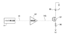
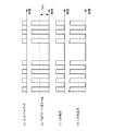
このような光時間領域反射測定器において、光ファイバに入射させるべきパルス光を出力するパルス光源として、例えば図8に示すようなものがある。図8は所謂レーザダイオード駆動回路の構成であり、パルス信号VIを生成するパルス発生器11と、パルス信号VIを増幅する増幅器92と、レーザダイオード98と、レーザダイオード98の駆動電流を調整する抵抗96と、レーザダイオード98の駆動電流をオンオフ制御するFET(電界効果トランジスタ)97と、を備えた構成である。
In such an optical time domain reflectometer, as a pulsed light source that outputs pulsed light to be incident on an optical fiber, there is, for example, one as shown in FIG. FIG. 8 shows a configuration of a so-called laser diode drive circuit, which includes a
この従来のレーザダイオード駆動回路では、図9に示すように、パルス発生器11でパルス列(図9(a)参照)が生成され、増幅器92で増幅された信号がFET97のゲート電極に印加される(図9(b)参照)。これによりFET97がオンオフ制御され、FET97がオン時にレーザダイオード98に駆動電流が流れ(図9(c)参照)、レーザダイオード98が発光して、図9(d)に示すような光パルスが得られる。
In this conventional laser diode drive circuit, as shown in FIG. 9, a pulse train (see FIG. 9A) is generated by the
ところで、レーザダイオードには温度依存性があることが知られている。つまり、レーザダイオードに流れる電流によりレーザダイオード素子自体が自己発熱し、例えば図9(d)に示すように、先行の光パルスの出力レベルに比べて後続の光パルスの出力レベルが下がってしまうこととなる。特に、光時間領域反射測定器において符号変調した光パルス列を用いる場合には、各光パルスの出力レベルが異なってしまうと、復調(逆拡散処理)において誤差が生じ、結果として測定精度が低下するという事情があった。 Incidentally, it is known that a laser diode has temperature dependency. That is, the laser diode element itself self-heats due to the current flowing through the laser diode, and the output level of the subsequent light pulse is lowered as compared with the output level of the preceding light pulse, for example, as shown in FIG. It becomes. In particular, when an optical pulse train that is code-modulated in an optical time domain reflectometer is used, if the output level of each optical pulse differs, an error occurs in demodulation (despreading processing), resulting in a decrease in measurement accuracy. There was a circumstance.
このようなレーザダイオードの温度依存性に対処する従来手法として、例えば、ペルチェ素子を用いてレーザダイオードの温度自体を一定に保つよう温度補償を行うことが一般的に知られている。しかしながら、光時間領域反射測定器では高速光パルス列(符号変調光パルス列の周期は概ね数十[ナノ秒])を使用するので、このペルチェ素子による温度補償だけでは応答が追いつかない。 As a conventional method for dealing with such temperature dependency of the laser diode, for example, it is generally known to perform temperature compensation using a Peltier element so that the temperature of the laser diode itself is kept constant. However, since the optical time domain reflectometer uses a high-speed optical pulse train (the period of the code-modulated optical pulse train is approximately several tens of nanoseconds), the response cannot be caught up only by temperature compensation using this Peltier element.
また、特開平8−236849号公報にも開示されているように、レーザダイオード駆動回路において、光出力を一定にするためのAPC回路を用いる構成もあるが、APC回路は光出力のモニタ信号に基づくフィードバック制御であることから応答が遅く、その結果、高速光パルス列の出力レベルがばらついてしまうという事情があった。 In addition, as disclosed in Japanese Patent Laid-Open No. 8-236849, there is a configuration in which an APC circuit for making the optical output constant is used in the laser diode driving circuit, but the APC circuit is used as a monitor signal for optical output. Since the feedback control is based, the response is slow, and as a result, the output level of the high-speed optical pulse train varies.
本発明は、上記従来の事情に鑑みてなされたものであって、一様な光出力レベルの高速光パルス列を生成し得るレーザダイオード駆動回路を提供することを目的としている。 The present invention has been made in view of the above-described conventional circumstances, and an object thereof is to provide a laser diode drive circuit capable of generating a high-speed optical pulse train having a uniform optical output level.
また、本発明の他の目的は、レーザダイオードの温度依存性による光出力レベルのバラツキを抑制して高精度測定を可能とした光時間領域反射測定器を提供することにある。 Another object of the present invention is to provide an optical time domain reflectometer capable of performing high-accuracy measurement by suppressing variations in light output level due to temperature dependency of a laser diode.
上記課題を解決するために、本発明に係るレーザダイオード駆動回路は、レーザダイオードの駆動電流をオンオフ制御するスイッチング素子と、パルス信号を積分して前記スイッチング素子の制御電極に供給する積分回路と、を備えたことを特徴とする。 In order to solve the above problems, a laser diode driving circuit according to the present invention includes a switching element that controls on / off of a driving current of a laser diode, an integration circuit that integrates a pulse signal and supplies the pulse signal to a control electrode of the switching element, It is provided with.
また、上記発明において、前記パルス信号を出力するパルス発生器と、前記パルス信号を増幅する増幅器と、を備え、前記積分回路は、前記増幅器で増幅されたパルス信号を積分して前記スイッチング素子の制御電極に供給することを特徴とする。 Further, in the above invention, a pulse generator that outputs the pulse signal and an amplifier that amplifies the pulse signal, and the integration circuit integrates the pulse signal amplified by the amplifier to It supplies to a control electrode, It is characterized by the above-mentioned.
また、上記発明において、前記パルス信号を出力するパルス発生器と、入力信号を増幅して前記スイッチング素子の制御電極に供給する増幅器と、を備え、前記積分回路は、前記パルス信号を積分して前記増幅器に供給することを特徴とする。 Further, in the above invention, a pulse generator that outputs the pulse signal and an amplifier that amplifies the input signal and supplies the amplified signal to the control electrode of the switching element, and the integrating circuit integrates the pulse signal. The amplifier is supplied to the amplifier.
また、上記発明において、前記パルス信号を出力するパルス発生器と、入力信号を増幅する増幅器と、を備え、前記積分回路は、前記パルス信号を積分して前記増幅器に供給する第1積分回路と、前記増幅器で増幅されたパルス信号を積分して前記スイッチング素子の制御電極に供給する第2積分回路と、を備えたことを特徴とする。 Further, in the above invention, a pulse generator that outputs the pulse signal and an amplifier that amplifies the input signal, and the integration circuit integrates the pulse signal and supplies the pulse signal to the amplifier; And a second integration circuit that integrates the pulse signal amplified by the amplifier and supplies the pulse signal to the control electrode of the switching element.
また、上記発明において、前記積分回路または第1積分回路および第2積分回路、並びに前記スイッチング素子を持つ組を複数組並列接続したことを特徴とする。 In the above invention, a plurality of sets each including the integration circuit or the first integration circuit and the second integration circuit, and the switching element are connected in parallel.
また、上記発明において、前記積分回路、第1積分回路または第2積分回路は、一端に積分すべき信号が入力される第1抵抗と、一端が前記第1抵抗の他端と接続される第2抵抗と、一端が前記第2抵抗の他端と接続され、他端が電源電位と接続されるキャパシタと、を備え、前記第1抵抗の他端から積分信号を出力することを特徴とする。 In the above invention, the integration circuit, the first integration circuit, or the second integration circuit includes a first resistor to which a signal to be integrated is input at one end and a first resistor connected to the other end of the first resistor. And a capacitor having one end connected to the other end of the second resistor and the other end connected to a power supply potential, and outputting an integration signal from the other end of the first resistor. .
さらに、測定対象に入射させるべきパルス光を出力するパルス光源と、前記パルス光源から出力されるパルス光を前記測定対象に入射させて得られる後方散乱光を受光する受光手段と、を備え、前記受光手段から出力される受光信号に基づき前記測定対象の長さ方向における所定物理量を測定する光時間領域反射測定器であって、請求項1〜請求項6の何れか1項に記載のレーザダイオード駆動回路により駆動されるレーザダイオードを前記パルス光源として備えたことを特徴とする。 Furthermore, a pulse light source that outputs a pulsed light to be incident on the measurement object, and a light receiving unit that receives backscattered light obtained by making the pulsed light output from the pulse light source incident on the measurement object, and The laser diode according to any one of claims 1 to 6, wherein the laser diode is an optical time domain reflectometer that measures a predetermined physical quantity in a length direction of the measurement object based on a light reception signal output from a light receiving means. A laser diode driven by a drive circuit is provided as the pulse light source.
本発明に係るレーザダイオード駆動回路によれば、一様な光出力レベルの高速光パルス列を生成し得るレーザダイオード駆動回路を提供することができる。また、本発明に係る光時間領域反射測定器によれば、レーザダイオードの温度依存性による光出力レベルのバラツキを抑制して高精度測定を可能とした光時間領域反射測定器を提供することができる。 The laser diode driving circuit according to the present invention can provide a laser diode driving circuit capable of generating a high-speed optical pulse train having a uniform optical output level. In addition, according to the optical time domain reflectometer according to the present invention, it is possible to provide an optical time domain reflectometer capable of performing high-accuracy measurement by suppressing variation in the optical output level due to the temperature dependence of the laser diode. it can.
以下、本発明に係る好適な実施の形態について、図面を参照しながら詳細に説明する。 DESCRIPTION OF EMBODIMENTS Hereinafter, preferred embodiments according to the present invention will be described in detail with reference to the drawings.
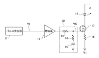
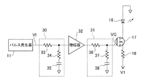
図1は本発明の一実施例に係るレーザダイオード駆動回路の構成図であり、図2は本実施例のレーザダイオード駆動回路における各種信号波形を例示する説明図である。なお、図1において図8(従来例)と重複する部分には同一の符号を附する。 FIG. 1 is a configuration diagram of a laser diode driving circuit according to an embodiment of the present invention, and FIG. 2 is an explanatory diagram illustrating various signal waveforms in the laser diode driving circuit of the present embodiment. 1 that are the same as those in FIG. 8 (conventional example) are denoted by the same reference numerals.
図1において、本実施例のレーザダイオード駆動回路は、パルス信号VIを生成するパルス発生器11と、パルス信号VIを増幅する増幅器12と、レーザダイオード18と、レーザダイオード18の駆動電流を調整する抵抗16と、レーザダイオード18の駆動電流をオンオフ制御するFET(電界効果トランジスタ)17と、増幅器12で増幅されたパルス信号を積分してFET17のゲート電極に供給する積分回路10と、を備えて構成されている。
In FIG. 1, the laser diode drive circuit of this embodiment adjusts the drive current of the
なお本実施例では、特許請求範囲にいうスイッチング素子としてn型MOS−FET(電界効果トランジスタ)を使用しており、制御電極はゲート電極となる。したがって、レーザダイオード18のアノードは接地電位に、カソードはFET17のドレイン電極にそれぞれ接続される。また、積分回路10は、一端に積分すべき信号(増幅器12で増幅されたパルス信号)が入力される第1抵抗13と、一端が第1抵抗13の他端と接続される第2抵抗14と、一端が第2抵抗14の他端と接続され、他端が電源電位(接地電位)と接続されるキャパシタ15と、を備えた構成である。
In this embodiment, an n-type MOS-FET (field effect transistor) is used as a switching element in the claims, and the control electrode is a gate electrode. Therefore, the anode of the
本実施例のレーザダイオード駆動回路では、図2に示すように、パルス発生器11でパルス列(図2(a)参照)が生成され、増幅器12で増幅された信号が積分回路10に供給される(図9(b)の破線参照)。積分回路10では、第1抵抗13のインピーダンスと第2抵抗14およびキャパシタ15の直列インピーダンスとで分配された電圧が出力される。すなわち、パルスの立ち上がり時には、第1抵抗13と第2抵抗14とで分配された電圧が出力され、その後積分回路10の時定数に従って徐々に増加していき、積分回路10の出力、即ちFET17のゲート電圧VGは図2(b)に示す如くなる。
In the laser diode driving circuit of the present embodiment, as shown in FIG. 2, a pulse train (see FIG. 2A) is generated by the
また、FET17のゲート電圧VGがFET97のスレッショルド電圧Vthを超えた時点でFET97がオンし、ゲート電圧VGがスレッショルド電圧Vthを下回った時点でFET97がオフとなり、レーザダイオード18の駆動電流は図2(c)に示す如くなる。さらに、レーザダイオード18からは、図2(d)に示すように、駆動電流に応じた光出力レベルの光パルスが発せられることとなる。
Further, when the gate voltage VG of the
なお、積分回路10を構成する各素子のパラメータはレーザダイオード18の種別に応じて定まり、予め行われる(シミュレーション)実験によって、光パルス列の光出力レベルが一様となるように第1抵抗13、第2抵抗14およびキャパシタ15の値が設定されているものとする。つまり、レーザダイオード18の温度依存性(レーザダイオード18に流れる駆動電流による自己発熱)による光出力レベルの低下分が積分回路10の積分動作によって相殺されるように各素子のパラメータが設定される。具体的数値を例示すれば、例えば光パルス列の周期が約20[ナノ秒]の場合、第1抵抗13および第2抵抗14はそれぞれ10〜数百[Ω]程度の値に、キャパシタ15の容量値は100[pF]程度の値にそれぞれ設定される。
The parameters of each element constituting the integrating
以上説明したように、本実施例のレーザダイオード駆動回路では、レーザダイオード18の駆動電流をオンオフ制御するスイッチング素子(FET17)と、増幅器12で増幅されたパルス信号を積分してスイッチング素子の制御電極(FET17のゲート電極)に供給する積分回路10と、を備え、レーザダイオード18の温度依存性による光出力レベルの低下分を積分回路10の積分動作によって相殺するようにしたので、一様な光出力レベルの高速光パルス列を生成し得るレーザダイオード駆動回路を実現することができる。
As described above, in the laser diode drive circuit of the present embodiment, the switching element (FET 17) that controls on / off of the drive current of the
なお、レーザダイオード18の温度依存性による光出力レベルの低下をキャンセルする他の手法として、例えば、パルス発生器11の出力側にDA変換器を付加して、パルス信号VIの1つ1つのパルスの振幅を調整して光出力レベルの低下分を補う構成も考えられる。しかしながら、この構成では高速動作のDA変換器を必要とし、また付随回路も必要となるため、回路部品が増えると共に装置コストも上昇してしまう。これに対して、本実施例のレーザダイオード駆動回路では、積分回路10の追加のみで済むことから、より簡単な構成で装置コストを抑制しつつ、一様な光出力レベルの高速光パルス列を生成し得るレーザダイオード駆動回路を実現することができる。
As another method for canceling the decrease in the optical output level due to the temperature dependency of the
次に、以上説明した実施例のレーザダイオード駆動回路を備えた光時間領域反射測定器について説明する。本発明に係る光時間領域反射測定器は、上記レーザダイオード駆動回路により駆動されるレーザダイオード18をパルス光源として備え、該パルス光源から出力される高速光パルス列を測定対象である光ファイバ112に入射させ、得られる反射光または散乱光を受光して、該受光信号に基づき光ファイバ112の長さ方向における所定物理量(損失量等)を測定するものである。
Next, an optical time domain reflectometer equipped with the laser diode drive circuit of the embodiment described above will be described. An optical time domain reflection measuring instrument according to the present invention includes a
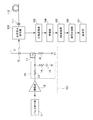
図3は本発明の実施例に係る光時間領域反射測定器の構成図である。同図において、パルス発生器11、レーザダイオード駆動回路101、光方向性結合器102、光電変換器103、増幅器104、AD変換器105、信号処理部106および表示部107を備えた構成である。
FIG. 3 is a block diagram of an optical time domain reflectometer according to an embodiment of the present invention. In the figure, a
ここで、パルス発生器11は、例えばゴーレイ符号(Golay code)やバーカー符号(Barker code)等で符号変調したパルス信号を出力する。そして、上述したレーザダイオード駆動回路101の構成により、レーザダイオード18からは、符号変調した一様な光出力レベルの高速光パルス列が発せられる。
Here, the
また、光方向性結合器102は、測定コネクタ111を介して光パルス列を光ファイバ112に向けて透過させるとともに、光ファイバ112からの戻り光を光電変換器103に向けて射出する。なお、光ファイバ112からの戻り光には、後方レイリー散乱光、フレネル反射光等が含まれる。
The optical
また、光電変換器103は、光方向性結合器102を介した光ファイバ112からの戻り光を電気信号に変換して増幅器104に出力する。ここで、光ファイバ112からの戻り光、特に後方レイリー散乱光は極めて微弱なため、光電変換器103には高感度のAPD(アバランシェ・フォトダイオード)を用いることが多い。APDに対する印加電圧(逆バイアス)を増加させることで増倍度を高くすることができ、これにより受光手段を高感度にすることができる。
Further, the
また、増幅器104は、光電変換器103から出力される電気信号(受光信号)を所定の増幅率で増幅してAD変換器105に出力する。AD変換器105は、増幅器104から出力される受光信号(アナログ信号)をサンプリングしてディジタル信号(受光データ)に変換して信号処理部106に出力する。なお、AD変換器105から出力される受光データは、光ファイバ112からの戻り光の強度変化を示す時系列データとなる。
The
また、信号処理部106は、AD変換器105から出力される受光データに対して復調(逆拡散)処理、平均化処理、レベル補正処理、並びにその他の演算処理を施すことにより光ファイバ112の長さ方向における所定物理量(損失量等)およびその分布を求める。また、表示部107は、CRTまたは液晶表示装置等で具現され、信号処理部106で求められた光ファイバ112の長さ方向における所定物理量の分布等を表示する。
In addition, the
上記構成において、パルス光源(レーザダイオード18)から出力された高速光パルス列は、光方向性結合器102を介して光ファイバ112に入射され光ファイバ112中を伝播する。光パルスが光ファイバ112中を伝播することによって後方レイリー散乱光が発生し、光パルスが光ファイバ112の他端に至るとフレネル反射光が発生する。これら後方レイリー散乱光およびフレネル反射光を含む戻り光は、光方向性結合器102を介して光電変換器103に入射して受光信号に変換される。
In the above configuration, the high-speed optical pulse train output from the pulse light source (laser diode 18) enters the
光電変換器103から出力された受光信号は増幅器104で増幅された後に、AD変換器105に入力され、所定タイミング信号に同期したサンプリングによりディジタル信号の受光データに変換される。AD変換器105で変換された受光データは、信号処理部106に入力され、復調(逆拡散)処理、平均化処理、レベル補正処理、並びにその他の演算処理が施され、これにより、光ファイバ112の長さ方向における所定物理量(損失量等)およびその分布が求められて表示部107に表示されることとなる。
The light reception signal output from the
以上説明したように、本実施例の光時間領域反射測定器においては、パルス光源(レーザダイオード18)から一様な光出力レベルの高速光パルス列が発せられるので、復調(逆拡散)処理における誤差や歪みを抑制することができ、結果として高精度に損失量等の測定が可能な光時間領域反射測定器を実現することができる。 As described above, in the optical time domain reflectometer of the present embodiment, a high-speed optical pulse train having a uniform optical output level is emitted from the pulse light source (laser diode 18), and therefore an error in demodulation (despreading) processing. As a result, it is possible to realize an optical time domain reflectometer capable of measuring a loss amount and the like with high accuracy.
なお、本実施例では光時間領域反射測定器(OTDR)の基本的な構成について例示したが、これに限定されることなく種々の変形、変更が可能である。例えば、光ファイバのブリルアン散乱光の周波数シフト量が歪みに比例して変化することを利用して、光ファイバの歪み分布を測定するB−OTDR(Brillouin Optical Time-Domain Reflect-meter)に適用した場合には、光ファイバ内に発生する歪みとその位置を光ファイバ片端から連続的に測定して、光ファイバの歪み量を高精度に測定することができる。 In addition, although the present Example illustrated about the basic structure of the optical time domain reflection measuring device (OTDR), various deformation | transformation and a change are possible, without being limited to this. For example, the present invention is applied to a B-OTDR (Brillouin Optical Time-Domain Reflect-meter) that measures the strain distribution of an optical fiber by utilizing the fact that the frequency shift amount of the Brillouin scattered light of the optical fiber changes in proportion to the strain. In this case, the strain generated in the optical fiber and its position can be continuously measured from one end of the optical fiber, and the strain amount of the optical fiber can be measured with high accuracy.
また、ラマン散乱光を構成する2成分、つまり入射光よりも低い周波数側へシフトしたストークス成分と入射光よりも高い周波数側へシフトした反ストークス成分との各強度の相対関係(例えば、強度比等)が光ファイバの温度に依存することを利用して、光ファイバの温度分布を測定するR−OTDR(Raman Optical-Time Domain Reflect-meter)に適用した場合には、戻り光の戻り時間から光ファイバの長手方向における位置を検出して、光ファイバの長手方向における温度分布を検出することで、光ファイバの温度を高精度に測定することができる。
(変形例1)
Also, the relative relationship between the two components constituting the Raman scattered light, that is, the Stokes component shifted to the lower frequency side than the incident light and the anti-Stokes component shifted to the higher frequency side than the incident light (for example, the intensity ratio) Etc.) is applied to an R-OTDR (Raman Optical-Time Domain Reflect-meter) that measures the temperature distribution of the optical fiber by utilizing the dependence on the temperature of the optical fiber. By detecting the position in the longitudinal direction of the optical fiber and detecting the temperature distribution in the longitudinal direction of the optical fiber, the temperature of the optical fiber can be measured with high accuracy.
(Modification 1)
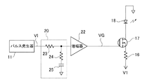
次に、本発明に係るレーザダイオード駆動回路の種々の変形について説明する。図4は本発明の変形例1に係るレーザダイオード駆動回路の構成図である。なお、図4において図1(実施例)と重複する部分には同一の符号を附する。図4において、本変形例のレーザダイオード駆動回路は、パルス信号VIを生成するパルス発生器11と、パルス信号VIを積分して出力する積分回路20と、積分回路20の出力を増幅する増幅器22と、レーザダイオード18と、抵抗16と、FET17と、を備えて構成されている。また、積分回路20は、一端にパルス信号VIが入力される第1抵抗23と、一端が第1抵抗23の他端と接続される第2抵抗24と、一端が第2抵抗24の他端と接続され、他端が電源電位(接地電位)と接続されるキャパシタ25と、を備えた構成である。
Next, various modifications of the laser diode drive circuit according to the present invention will be described. FIG. 4 is a configuration diagram of a laser diode drive circuit according to the first modification of the present invention. 4 that are the same as those in FIG. 1 (the embodiment) are denoted by the same reference numerals. In FIG. 4, the laser diode drive circuit of the present modification includes a
実施例では積分回路10を増幅器12とFET17との間に挿入した構成(図1)としたのに対し、本変形例では積分回路10をパルス発生器11とFET17との間に挿入した構成としている。本変形例の構成によっても、実施例と同様に、レーザダイオード18の温度依存性による光出力レベルの低下分が積分回路20の積分動作によって相殺されるように積分回路20の各素子のパラメータを設定することで、レーザダイオード18から一様な光出力レベルの高速光パルス列が発せられるようにすることができる。
(変形例2)
In the embodiment, the
(Modification 2)
次に、図5は本発明の変形例2に係るレーザダイオード駆動回路の構成図である。なお、図5において図1(実施例)と重複する部分には同一の符号を附する。図5において、本変形例のレーザダイオード駆動回路は、パルス信号VIを生成するパルス発生器11と、パルス信号VIを積分して出力する第1積分回路30と、積分回路20の出力を増幅する増幅器32と、増幅器32の出力を積分してFET17のゲート電極に供給する第2積分回路31と、レーザダイオード18と、抵抗16と、FET17と、を備えて構成されている。
Next, FIG. 5 is a block diagram of a laser diode driving circuit according to the second modification of the present invention. 5 that are the same as those in FIG. 1 (the embodiment) are denoted by the same reference numerals. In FIG. 5, the laser diode drive circuit of this modification example amplifies the output of the
また、第1積分回路30は、一端にパルス信号VIが入力される第1抵抗33と、一端が第1抵抗33の他端と接続される第2抵抗34と、一端が第2抵抗34の他端と接続され、他端が電源電位(接地電位)と接続されるキャパシタ35と、を備えた構成であり、第2積分回路31は、一端に増幅器32の出力が入力される第1抵抗36と、一端が第1抵抗36の他端と接続される第2抵抗37と、一端が第2抵抗37の他端と接続され、他端が電源電位(接地電位)と接続されるキャパシタ38と、を備えた構成である。
The first integrating
本変形例では、第1積分回路30をパルス発生器11と増幅器32との間に挿入し、第2積分回路31を増幅器32とFET17との間に挿入した構成としている。本変形例の構成によっても、レーザダイオード18の温度依存性による光出力レベルの低下分が第1積分回路30および第2積分回路31の積分動作によって相殺されるように第1積分回路30および第2積分回路31の各素子のパラメータを設定することで、レーザダイオード18から一様な光出力レベルの高速光パルス列が発せられるようにすることができる。なお、実施例および変形例1と比較して調整可能な回路パラメータが倍に増えることにより、きめ細かく調整することができ、レーザダイオード18から発せられる光出力レベルのバラツキをより低減することができる。
(変形例3)
In this modification, the
(Modification 3)
次に、図6は本発明の変形例3に係るレーザダイオード駆動回路の構成図である。なお、図6において図1(実施例)と重複する部分には同一の符号を附する。図6において、本変形例のレーザダイオード駆動回路は、パルス信号VIを生成するパルス発生器11と、パルス信号VIを増幅する増幅器42と、増幅器42の出力を積分して出力する第1積分回路41および第2積分回路51と、レーザダイオード18と、第1電流調整用抵抗46および第2電流調整用抵抗56と、第1FET47および第2FET57と、を備えて構成されている。
Next, FIG. 6 is a block diagram of a laser diode drive circuit according to the third modification of the present invention. 6 that are the same as those in FIG. 1 (the embodiment) are denoted by the same reference numerals. In FIG. 6, the laser diode drive circuit of the present modification includes a
また、第1積分回路41は、一端にパルス信号VIが入力される第1抵抗43と、一端が第1抵抗43の他端と接続される第2抵抗44と、一端が第2抵抗44の他端と接続され、他端が電源電位(接地電位)と接続されるキャパシタ45と、を備えた構成であり、第2積分回路51は、一端にパルス信号VIが入力される第1抵抗53と、一端が第1抵抗53の他端と接続される第2抵抗54と、一端が第2抵抗54の他端と接続され、他端が電源電位(接地電位)と接続されるキャパシタ55と、を備えた構成である。
The
本変形例では、積分回路、FETおよび電流調整用抵抗を2組並列接続した構成としている。本変形例の構成によっても、レーザダイオード18の温度依存性による光出力レベルの低下分が第1積分回路41および第2積分回路51の積分動作によって相殺されるように第1積分回路41および第2積分回路51の各素子のパラメータを設定することで、レーザダイオード18から一様な光出力レベルの高速光パルス列が発せられるようにすることができる。なお、実施例および変形例1と比較して調整可能な回路パラメータが倍に増えることにより、きめ細かく調整することができ、レーザダイオード18から発せられる光出力レベルのバラツキをより低減することができる。
(変形例4)
In this modification, two sets of integrating circuits, FETs, and current adjusting resistors are connected in parallel. Even in the configuration of this modification, the
(Modification 4)
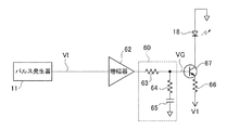
次に、図7は本発明の変形例4に係るレーザダイオード駆動回路の構成図である。なお、図7において図1(実施例)と重複する部分には同一の符号を附する。図7において、本変形例のレーザダイオード駆動回路は、パルス信号VIを生成するパルス発生器11と、パルス信号VIを増幅する増幅器62と、増幅器62の出力を積分して出力する積分回路60と、レーザダイオード18と、抵抗66と、バイポーラトランジスタ67と、を備えて構成されている。
Next, FIG. 7 is a block diagram of a laser diode driving circuit according to the fourth modification of the present invention. 7 that are the same as those in FIG. 1 (the embodiment) are denoted by the same reference numerals. In FIG. 7, the laser diode drive circuit according to the present modification includes a
本変形例では、特許請求範囲にいうスイッチング素子としてバイポーラトランジスタを使用しており、制御電極はベース電極となる。また、積分回路60は、一端に増幅器62で増幅されたパルス信号が入力される第1抵抗63と、一端が第1抵抗63の他端と接続される第2抵抗64と、一端が第2抵抗64の他端と接続され、他端が電源電位(接地電位)と接続されるキャパシタ65と、を備えた構成である。
In this modification, a bipolar transistor is used as the switching element in the claims, and the control electrode serves as a base electrode. The integrating
本変形例の構成によっても、レーザダイオード18の温度依存性による光出力レベルの低下分が積分回路60の積分動作によって相殺されるように積分回路60の各素子のパラメータを設定することで、レーザダイオード18から一様な光出力レベルの高速光パルス列が発せられるようにすることができる。
Even in the configuration of this modification, the parameters of each element of the
また、上述した変形例1〜変形例4のレーザダイオード駆動回路により駆動されるレーザダイオード18をパルス光源として、光時間領域反射測定器を構成した場合には、実施例と同様に、レーザダイオード18から一様な光出力レベルの高速光パルス列が発せられるので、復調(逆拡散)処理における誤差や歪みを抑制することができ、結果として高精度に物理量(損失、歪みまたは温度等)の測定が可能な光時間領域反射測定器を実現することができる。
(その他の変形)
Further, in the case where the optical time domain reflection measuring device is configured by using the
(Other variations)
以上、本発明の好ましい実施例および変形例について詳述したが、本発明に係るレーザダイオード駆動回路および光時間領域反射測定器は、上述した実施例および変形例に限定されるものではなく、特許請求の範囲に記載された本発明の要旨の範囲内において、種々の変形、変更が可能である。 The preferred embodiments and modifications of the present invention have been described in detail above. However, the laser diode driving circuit and the optical time domain reflectometer according to the present invention are not limited to the above-described embodiments and modifications, and are patented. Various modifications and changes are possible within the scope of the gist of the present invention described in the claims.
例えば、実施例および変形例1〜変形例3では、スイッチング素子としてn型MOS−FETを使用したが、p型MOS−FETで代替しても良い。この場合、パルス信号VIの極性は逆となり、レーザダイオード18のアノードはFET17のドレイン電極に、カソードは接地電位にそれぞれ接続される。また、変形例4ではnpnトランジスタを使用したが、pnpトランジスタで代替しても良い。この場合、パルス信号VIの極性は逆となり、レーザダイオード18のアノードはpnpトランジスタのコレクタ電極に、カソードは接地電位にそれぞれ接続される。さらに、スイッチング素子としては、MOS−FETやバイポーラトランジスタに限定されることなく、他のスイッチング素子を使用することも可能である。
For example, in the embodiment and the first to third modifications, an n-type MOS-FET is used as a switching element, but a p-type MOS-FET may be used instead. In this case, the polarity of the pulse signal VI is reversed, and the anode of the
10,20,30,31,41,51,60 積分回路
11 パルス発生器
12,22,32,42,62 増幅器
13,23,33,36,43,53,63 第1抵抗
14,24,34,37,44,54,64 第2抵抗
15,25,35,38,45,55,65 キャパシタ
16,46,56,66 (電流調整用)抵抗
17,47,57 FET(電界効果トランジスタ)
67 バイポーラトランジスタ
101 レーザダイオード駆動回路
102 光方向性結合器
103 光電変換器
104 増幅器
105 AD変換器
106 信号処理部
107 表示部
112 光ファイバ
10, 20, 30, 31, 41, 51, 60
67
Claims (7)
パルス信号を積分して前記スイッチング素子の制御電極に供給する積分回路と、
を備えたことを特徴とするレーザダイオード駆動回路。 A switching element that controls on / off of the drive current of the laser diode;
An integration circuit that integrates a pulse signal and supplies it to the control electrode of the switching element;
A laser diode driving circuit comprising:
前記積分回路は、前記増幅器で増幅されたパルス信号を積分して前記スイッチング素子の制御電極に供給することを特徴とする請求項1に記載のレーザダイオード駆動回路。 A pulse generator that outputs the pulse signal; and an amplifier that amplifies the pulse signal,
2. The laser diode driving circuit according to claim 1, wherein the integrating circuit integrates the pulse signal amplified by the amplifier and supplies the integrated pulse signal to a control electrode of the switching element.
前記積分回路は、前記パルス信号を積分して前記増幅器に供給することを特徴とする請求項1に記載のレーザダイオード駆動回路。 A pulse generator that outputs the pulse signal, and an amplifier that amplifies the input signal and supplies the amplified signal to the control electrode of the switching element,
The laser diode driving circuit according to claim 1, wherein the integrating circuit integrates the pulse signal and supplies the integrated pulse signal to the amplifier.
前記積分回路は、
前記パルス信号を積分して前記増幅器に供給する第1積分回路と、
前記増幅器で増幅されたパルス信号を積分して前記スイッチング素子の制御電極に供給する第2積分回路と、
を備えることを特徴とする請求項1に記載のレーザダイオード駆動回路。 A pulse generator for outputting the pulse signal, and an amplifier for amplifying the input signal,
The integration circuit includes:
A first integrating circuit for integrating the pulse signal and supplying the integrated signal to the amplifier;
A second integrating circuit for integrating the pulse signal amplified by the amplifier and supplying the pulse signal to the control electrode of the switching element;
The laser diode driving circuit according to claim 1, further comprising:
一端に積分すべき信号が入力される第1抵抗と、
一端が前記第1抵抗の他端と接続される第2抵抗と、
一端が前記第2抵抗の他端と接続され、他端が電源電位と接続されるキャパシタと、
を備え、前記第1抵抗の他端から積分信号を出力することを特徴とする請求項1〜請求項5の何れか1項に記載のレーザダイオード駆動回路。 The integrating circuit, the first integrating circuit or the second integrating circuit is:
A first resistor to which a signal to be integrated is input at one end;
A second resistor having one end connected to the other end of the first resistor;
A capacitor having one end connected to the other end of the second resistor and the other end connected to a power supply potential;
The laser diode drive circuit according to claim 1, further comprising: an integrated signal output from the other end of the first resistor.
請求項1〜請求項6の何れか1項に記載のレーザダイオード駆動回路により駆動されるレーザダイオードを前記パルス光源として備えることを特徴とする光時間領域反射測定器。 A pulse light source that outputs a pulsed light to be incident on the measurement object; and a light receiving unit that receives reflected light or scattered light obtained by making the pulse light output from the pulse light source incident on the measurement object, and An optical time domain reflectometer for measuring a predetermined physical quantity in the length direction of the measurement object based on a light reception signal output from a light receiving means,
An optical time domain reflectometer comprising a laser diode driven by the laser diode driving circuit according to claim 1 as the pulse light source.
Priority Applications (1)
| Application Number | Priority Date | Filing Date | Title |
|---|---|---|---|
| JP2011016585A JP2012156458A (en) | 2011-01-28 | 2011-01-28 | Laser diode drive circuit and optical time-domain reflection measurement instrument |
Applications Claiming Priority (1)
| Application Number | Priority Date | Filing Date | Title |
|---|---|---|---|
| JP2011016585A JP2012156458A (en) | 2011-01-28 | 2011-01-28 | Laser diode drive circuit and optical time-domain reflection measurement instrument |
Publications (1)
| Publication Number | Publication Date |
|---|---|
| JP2012156458A true JP2012156458A (en) | 2012-08-16 |
Family
ID=46837841
Family Applications (1)
| Application Number | Title | Priority Date | Filing Date |
|---|---|---|---|
| JP2011016585A Pending JP2012156458A (en) | 2011-01-28 | 2011-01-28 | Laser diode drive circuit and optical time-domain reflection measurement instrument |
Country Status (1)
| Country | Link |
|---|---|
| JP (1) | JP2012156458A (en) |
Cited By (4)
| Publication number | Priority date | Publication date | Assignee | Title |
|---|---|---|---|---|
| CN106707262A (en) * | 2016-11-18 | 2017-05-24 | 常州大地测绘科技有限公司 | Laser pulse transmission circuit |
| WO2019087524A1 (en) * | 2017-11-02 | 2019-05-09 | ソニー株式会社 | Semiconductor laser drive circuit, semiconductor laser drive circuit driving method, distance measuring device and electronic machine |
| CN110190505A (en) * | 2019-05-30 | 2019-08-30 | 苏州贝林激光有限公司 | The burst pulse drive system and its method of pulse laser |
| KR20200035733A (en) * | 2018-09-27 | 2020-04-06 | 엘지전자 주식회사 | Emitting ligth drive curcuit of laser diode and driving method thereof, a robot cleaner comprising the emitting ligth drive curcuit |
-
2011
- 2011-01-28 JP JP2011016585A patent/JP2012156458A/en active Pending
Cited By (9)
| Publication number | Priority date | Publication date | Assignee | Title |
|---|---|---|---|---|
| CN106707262A (en) * | 2016-11-18 | 2017-05-24 | 常州大地测绘科技有限公司 | Laser pulse transmission circuit |
| CN106707262B (en) * | 2016-11-18 | 2019-06-18 | 常州大地测绘科技有限公司 | Laser pulse emission circuit |
| WO2019087524A1 (en) * | 2017-11-02 | 2019-05-09 | ソニー株式会社 | Semiconductor laser drive circuit, semiconductor laser drive circuit driving method, distance measuring device and electronic machine |
| JPWO2019087524A1 (en) * | 2017-11-02 | 2020-11-26 | ソニー株式会社 | Semiconductor laser drive circuit, drive method of semiconductor laser drive circuit, distance measuring device and electronic equipment |
| JP7160045B2 (en) | 2017-11-02 | 2022-10-25 | ソニーグループ株式会社 | Semiconductor laser drive circuit, distance measuring device and electronic device |
| US11594855B2 (en) | 2017-11-02 | 2023-02-28 | Sony Corporation | Semiconductor laser drive circuit, method for driving semiconductor laser drive circuit, distance measuring apparatus, and electronic apparatus |
| KR20200035733A (en) * | 2018-09-27 | 2020-04-06 | 엘지전자 주식회사 | Emitting ligth drive curcuit of laser diode and driving method thereof, a robot cleaner comprising the emitting ligth drive curcuit |
| KR102521942B1 (en) * | 2018-09-27 | 2023-04-14 | 엘지전자 주식회사 | Emitting ligth drive curcuit of laser diode and driving method thereof, a robot cleaner comprising the emitting ligth drive curcuit |
| CN110190505A (en) * | 2019-05-30 | 2019-08-30 | 苏州贝林激光有限公司 | The burst pulse drive system and its method of pulse laser |
Similar Documents
| Publication | Publication Date | Title |
|---|---|---|
| JP6766815B2 (en) | Correction device, correction method and distance measuring device | |
| WO2007030700A3 (en) | Power monitor for monitoring input optical power incident on avalanche photodiodes | |
| TWI505588B (en) | Laser diode automatic stabilized optical power pulse driving device | |
| US20160003687A1 (en) | Optical fiber temperature distribution measuring device | |
| CN103875181B (en) | Optical power monitoring device and method | |
| JP2012156458A (en) | Laser diode drive circuit and optical time-domain reflection measurement instrument | |
| US9952104B2 (en) | Optical fiber temperature distribution measuring device | |
| US20130039663A1 (en) | Circuits, Architectures, Apparatuses, Methods and Algorithms for Determining a DC Bias in an AC or AC-Coupled Signal | |
| CN113203886A (en) | Method for controlling gain and sensitivity of electro-optical probe | |
| US20110222867A1 (en) | Optical Receiver Using Single Ended Voltage Offset Measurement | |
| JP2016014535A (en) | Distance measuring system | |
| CN101241025A (en) | Optical energy measuring device and optical signal receiving device equipped with the device | |
| JP5432885B2 (en) | Optical pulse tester having automatic adjustment function of APD or method thereof | |
| Kurtti et al. | An integrated receiver channel for a laser scanner | |
| JP5061981B2 (en) | Optical pulse tester and optical power stabilization method for optical pulse tester | |
| JP5273409B2 (en) | Optical receiver and light receiving current monitoring method | |
| US10495517B2 (en) | Method for noncontact, radiation thermometric temperature measurement | |
| JP5515199B2 (en) | Optical pulse test apparatus and adjustment method thereof | |
| JP2019105603A (en) | Temperature measuring device | |
| US7038187B2 (en) | Circuit for measuring photo-current level in fiber optic links | |
| CN102645764A (en) | Liquid crystal display (LCD) transmissivity testing method and device | |
| JP5748934B2 (en) | Optical pulse generator and optical pulse tester | |
| JP5118601B2 (en) | Optical pulse tester | |
| US20180074197A1 (en) | Distance measuring device | |
| JP5305032B2 (en) | Optical fiber distributed temperature measuring device |