JP2012156035A - Electron emission element, electron beam device, image display device and method of manufacturing the same - Google Patents

Electron emission element, electron beam device, image display device and method of manufacturing the same Download PDF

Info

Publication number
JP2012156035A
JP2012156035A JP2011014827A JP2011014827A JP2012156035A JP 2012156035 A JP2012156035 A JP 2012156035A JP 2011014827 A JP2011014827 A JP 2011014827A JP 2011014827 A JP2011014827 A JP 2011014827A JP 2012156035 A JP2012156035 A JP 2012156035A
Authority
JP
Japan
Prior art keywords
material layer
electron
conductive material
gate
emitting device
Prior art date
Legal status (The legal status is an assumption and is not a legal conclusion. Google has not performed a legal analysis and makes no representation as to the accuracy of the status listed.)
Withdrawn
Application number
JP2011014827A
Other languages
Japanese (ja)
Inventor
Katsushi Danjo
桂志 壇上
Toshiji Sumiya
利治 住谷
Current Assignee (The listed assignees may be inaccurate. Google has not performed a legal analysis and makes no representation or warranty as to the accuracy of the list.)
Canon Inc
Original Assignee
Canon Inc
Priority date (The priority date is an assumption and is not a legal conclusion. Google has not performed a legal analysis and makes no representation as to the accuracy of the date listed.)
Filing date
Publication date
Application filed by Canon Inc filed Critical Canon Inc
Priority to JP2011014827A priority Critical patent/JP2012156035A/en
Publication of JP2012156035A publication Critical patent/JP2012156035A/en
Withdrawn legal-status Critical Current

Links

Images

Abstract

PROBLEM TO BE SOLVED: To provide an electron emission element which has an insulating member which is disposed on a substrate and has at least one side surface portion rising from the surface of the substrate, a gate provided to the upper surface of the insulating member, a recess portion formed just below the gate of the side surface portion, and a cathode which projects upwards from the lower edge of the recess portion and has a projecting portion having plural apex portions formed in the length direction of the lower edge, and is enhanced in electron emission characteristic.SOLUTION: A cathode 6 is formed by using a first conductive material layer 6a formed by a sputtering method under a full pressure lower than 1.0 Pa, a second conductive material layer is formed by a sputtering method under a full pressure from 1.0 Pa to 2.8 Pa, the second conductive material layer is etched, and an auxiliary apex portion 9 is formed by using the second conductive material layer left on the inner slant surface of the apex portion 8 of the projecting portion, thereby increasing the number of electron emission points.

Description

本発明は、電界放出型の電子放出素子、この電子放出素子を用いた電子線装置、この電子線装置を用いた画像表示装置及びこれらの製造方法に関する。   The present invention relates to a field emission type electron-emitting device, an electron beam device using the electron-emitting device, an image display device using the electron beam device, and a manufacturing method thereof.

従来、電界放出型の電子放出素子として、特許文献1に示される電子放出素子が知られている。即ち、この特許文献1に示される電子放出素子は、基板上に配置され、基板の表面から立ち上がる少なくとも一の側面部を有する絶縁部材と、この絶縁部材の上面に設けられたゲートとを備えている。そして、上記側面部におけるゲートの直下には凹部が形成されており、この凹部の下縁から上方へ突起した突起部を有するカソードを備えている。また、特許文献1は、カソードの突起部が高さ分布を有していることを開示しており、しかもこの高さ分布を有する突起部とゲートとの距離を調整することで均一な電子放出特性の電子放出素子が得られることを開示している。   Conventionally, an electron-emitting device disclosed in Patent Document 1 is known as a field-emission electron-emitting device. That is, the electron-emitting device disclosed in Patent Document 1 includes an insulating member that is disposed on a substrate and has at least one side surface that rises from the surface of the substrate, and a gate that is provided on the upper surface of the insulating member. Yes. A concave portion is formed immediately below the gate in the side surface portion, and a cathode having a protruding portion protruding upward from the lower edge of the concave portion is provided. Patent Document 1 discloses that the protrusions of the cathode have a height distribution, and uniform electron emission by adjusting the distance between the protrusions having the height distribution and the gate. It is disclosed that a characteristic electron-emitting device can be obtained.

特開2010−262892号公報JP 2010-262892 A

特許文献1に示されるような電子放出素子は、突起部が高さ分布を有することで複数の頂部を備えており、この頂部に電界が集中しやすいことから、頂部から電子が放出されることになる。このため、突起部の頂部とゲートの距離を適切に調整することで良好な電子放出特性を得ることができる。   The electron-emitting device as shown in Patent Document 1 has a plurality of top portions because the protrusion has a height distribution, and the electric field tends to concentrate on the top portions, so that electrons are emitted from the top portions. become. Therefore, good electron emission characteristics can be obtained by appropriately adjusting the distance between the top of the protrusion and the gate.

しかしながら、例えばより性能の良い画像表示装置を得るためには更なる電子放出特性の向上が求められるが、突起部の頂部とゲートの距離調整だけでは電子放出特性の向上に限度があり、これに応じきれない問題がある。   However, for example, in order to obtain an image display device with higher performance, further improvement in electron emission characteristics is required. However, there is a limit to improvement in electron emission characteristics only by adjusting the distance between the top of the protrusion and the gate. There is a problem that cannot be met.

本発明は、上記従来の問題点に鑑みてなされたもので、ゲートと、このゲートと対向する突起部を有するカソードとを備え、突起部が複数の頂部を有する電子放出素子について、更なる電子放出特性の向上を計ることを目的とする。また、併せて、性能のよい電子源装置及び画像表示装置を得ることを目的とする。   The present invention has been made in view of the above-described conventional problems. An electron-emitting device including a gate and a cathode having a protrusion facing the gate, the protrusion having a plurality of apexes, further electrons. The purpose is to improve the release characteristics. In addition, another object is to obtain an electron source device and an image display device with good performance.

本発明の第一は、基板の上に配置され、該基板の表面から立ち上がる少なくとも一の側面部を有する絶縁部材と、該絶縁部材の上面に設けられたゲートと、前記側面部の前記ゲートの直下に形成された凹部と、該凹部の下縁から上方へ突起し、該下縁の長さ方向に複数の頂部が形成された突起部を有するカソードとを備えた電子放出素子の製造方法において、全圧が1.0Paよりも低い圧力下のスパッタリング法で形成した第一の導電材料層で前記カソードを形成した後、全圧が1.0Pa以上2.8Pa以下の圧力下のパッタリング法によって少なくとも前記突起部に第二の導電性材料層を形成し、該第二の導電性材料層をエッチングして、前記突起部の頂部の内側斜面に残留させた第二の導電材料層で副頂部を形成することを特徴とする電子放出素子の製造方法を提供するものである。   According to a first aspect of the present invention, there is provided an insulating member disposed on a substrate and having at least one side surface rising from the surface of the substrate, a gate provided on an upper surface of the insulating member, and the gate of the side surface portion. In a method of manufacturing an electron-emitting device, comprising: a concave portion formed immediately below; and a cathode having a plurality of top portions protruding upward from a lower edge of the concave portion and having a plurality of top portions formed in a length direction of the lower edge. After the cathode is formed with the first conductive material layer formed by a sputtering method under a pressure lower than 1.0 Pa in total pressure, a patterning method under a pressure of 1.0 Pa to 2.8 Pa in total pressure A second conductive material layer is formed at least on the protrusions by etching, and the second conductive material layer is etched so that the second conductive material layer is left on the inner slope of the top of the protrusions. Characterized by forming the top There is provided a method of manufacturing an electron-emitting device.

本発明の第二は、上記電子放出素子の製造方法で製造した電子放出素子を用いた電子線装置の製造方法を提供するもので、本発明の第三は、この電子線装置の製造方法で製造した電子線装置を用いた画像表示装置の製造方法を提供するものである。   The second aspect of the present invention provides a method for manufacturing an electron beam apparatus using the electron emitting element manufactured by the above method for manufacturing an electron emitting element, and the third aspect of the present invention is a method for manufacturing the electron beam apparatus. The present invention provides a method of manufacturing an image display device using the manufactured electron beam apparatus.

本発明の第四は、基板上に配置され、該基板の表面から立ち上がる少なくとも一の側面部を有する絶縁部材と、該絶縁部材の上面に設けられたゲートと、前記側面部の前記ゲートの直下に形成された凹部と、該凹部の下縁から上方へ突起し、該下縁の長さ方向に複数の頂部が形成された突起部を有するカソードとを備えた電子放出素子において、前記突起部の頂部の内側斜面に副頂部が形成されていることを特徴とする電子放出素子を提供するものである。   According to a fourth aspect of the present invention, there is provided an insulating member that is disposed on the substrate and has at least one side surface rising from the surface of the substrate, a gate provided on the upper surface of the insulating member, and a portion of the side surface portion directly below the gate. In the electron-emitting device, the protrusion includes a recess formed in the recess, and a cathode that protrudes upward from the lower edge of the recess and has a plurality of apexes formed in the length direction of the lower edge. An electron-emitting device characterized in that a sub-top is formed on the inner slope of the top.

本発明の第五は、上記電子放出素子を用いた電子線装置を提供するもので、本発明の第六は、この電子線装置を用いた画像表示装置を提供するものである。   A fifth aspect of the present invention provides an electron beam apparatus using the electron-emitting device, and a sixth aspect of the present invention provides an image display apparatus using the electron beam apparatus.

本発明に係る電子放出素子は、カソードの突起部に形成された頂部の内側斜面に副頂部が形成されてたものとなっている。この副頂部は、頂部と共に電解が集中しやすい凸部を構成し、電子放出点となる。このため、本発明に係る電子放出素子は、副頂部を有さない頂部のみの電子放出素子に比して、副頂部の数だけ電子放出点が多くなり、電子放出特性が向上されたものとなる。   The electron-emitting device according to the present invention is such that a sub-top is formed on the inner slope of the top formed on the projection of the cathode. This sub-top portion forms a convex portion where electrolysis tends to concentrate together with the top portion, and serves as an electron emission point. For this reason, the electron-emitting device according to the present invention has an electron emission point that is increased by the number of sub-tops, as compared with an electron-emitting device having only the top, which does not have a sub-top, and has improved electron emission characteristics. Become.

一方、本発明の製造方法によれば、第二の導電材料層は、第一の導電材料層に比して高い全圧下でのスパッタリングにより形成されていることにより、第一の導電材料層に比してエッチングされやすい状態とすることができる。このため、第一の導電材料層で形成したカソードの溶解を抑制しながら、第二の導電材料層を取り除くエッチング処理が可能である。ところで、カソードの突起部とゲートの間隔の中でも、特に突起部の頂部とゲートの間隔は狭く、この頂部の内側斜面はエッチングされにくい。その結果、第二の導電材料層のエッチング時に、頂部の内側斜面に第二の導電材料層が残留して副頂部を形成することができ、電子放出点を増やして、放出電流を増加させることができる。また、副頂部の形成時にゲートとの間隔を電子放出点として好ましい間隔に制御しやすくし、その結果、電子放出素子の均一性を向上させることができる。   On the other hand, according to the manufacturing method of the present invention, the second conductive material layer is formed by sputtering under a total pressure higher than that of the first conductive material layer. In contrast, it can be in a state where it is more easily etched. For this reason, the etching process which removes a 2nd conductive material layer is possible, suppressing melt | dissolution of the cathode formed with the 1st conductive material layer. By the way, among the gaps between the projections of the cathode and the gates, the gaps between the tops of the projections and the gates are particularly narrow, and the inner slopes of the tops are difficult to etch. As a result, when etching the second conductive material layer, the second conductive material layer can remain on the inner slope of the top to form a sub-top, increasing the electron emission point and increasing the emission current. Can do. In addition, when the sub-top portion is formed, the distance from the gate can be easily controlled as a preferable distance as an electron emission point, and as a result, the uniformity of the electron-emitting device can be improved.

上記本発明の電子放出素子又は本発明の製造方法で得た電子放出素子を用いて電子線装置を構成すると、上記のように電子放出特性の優れた電子放出素子を用いて電子線装置を構成することができ、性能の優れた電子線装置を製造することができる。また、この本発明の電子線装置を用いて画像表示装置を構成すると、より性能の良い画像表示装置とすることができる。   When an electron beam device is configured using the electron-emitting device of the present invention or the electron-emitting device obtained by the manufacturing method of the present invention, the electron beam device is configured using the electron-emitting device having excellent electron-emitting characteristics as described above. Therefore, an electron beam apparatus with excellent performance can be manufactured. Further, when an image display apparatus is configured using the electron beam apparatus of the present invention, an image display apparatus with better performance can be obtained.

本発明に係る電子放出素子の一例を示す模式図で、(a)は平面図、(b)は(a)におけるA−A断面図、(c)は正面図である。It is a schematic diagram which shows an example of the electron emission element which concerns on this invention, (a) is a top view, (b) is AA sectional drawing in (a), (c) is a front view. 図1に示す電子放出素子の部分拡大模式図で、(a)は凹部周りの拡大断面図、(b)は凹部周りの拡大正面図、(d)突起部の頂部付近の拡大断面図である。FIGS. 2A and 2B are partially enlarged schematic views of the electron-emitting device shown in FIG. 1, in which FIG. 1A is an enlarged sectional view around a concave portion, FIG. 1B is an enlarged front view around the concave portion, and FIG. . 本発明に係る電子放出素子の製造方法の工程の一例を示す説明図で、左側が断面図、右側が正面図である。It is explanatory drawing which shows an example of the process of the manufacturing method of the electron emission element which concerns on this invention, The left side is sectional drawing, The right side is a front view. 本発明に係る電子放出素子の製造方法の工程の一例を示す説明図で、左側が断面図、右側が正面図である。It is explanatory drawing which shows an example of the process of the manufacturing method of the electron emission element which concerns on this invention, The left side is sectional drawing, The right side is a front view. 本発明に係る電子放出素子の製造方法の工程の一例を示す説明図で、左側が断面図、右側が正面図である。It is explanatory drawing which shows an example of the process of the manufacturing method of the electron emission element which concerns on this invention, The left side is sectional drawing, The right side is a front view. 成膜時の圧力(成膜圧力)と得られる膜の密度との関係を示すグラフである。It is a graph which shows the relationship between the pressure at the time of film-forming (film-forming pressure), and the density of the film | membrane obtained. 導電性の膜における結晶粒部分と結晶粒界部分についての模式図で、(a)は低い圧力下で成膜した場合、(b)は高い圧力下で成膜した場合を示す。FIG. 4 is a schematic diagram of crystal grain portions and crystal grain boundary portions in a conductive film, where (a) shows a case where the film is formed under a low pressure, and (b) shows a case where the film is formed under a high pressure. スパッタリング時の全圧を変えた導電性膜についての、エッチング時間とエッチング量の関係を示すグラフである。It is a graph which shows the relationship between the etching time and the etching amount about the electroconductive film which changed the total pressure at the time of sputtering. スパッタリング時の全圧を変えた導電性膜についての、エッチング時間と間隔dの標準偏差σの変化を示すグラフである。It is a graph which shows the change of the standard deviation (sigma) of the etching time and the space | interval d about the electroconductive film which changed the total pressure at the time of sputtering. Moの第一の導電材料層をエッチングした時の変化の説明図である。It is explanatory drawing of the change when the 1st electrically-conductive material layer of Mo is etched. 第二の導電材料層のエッチング時の変化の説明図である。It is explanatory drawing of the change at the time of the etching of a 2nd conductive material layer. 電子線装置及び電子放出特性の測定系の説明図である。It is explanatory drawing of the measuring system of an electron beam apparatus and an electron emission characteristic. ディスプレィパネル、画像表示装置及びテレビジョン装置の説明図である。It is explanatory drawing of a display panel, an image display apparatus, and a television apparatus.

以下、図面を参照して、好適な実施の形態を例示的に詳しく説明する。ただし、この実施の形態に記載されている構成部品の寸法、材質、形状、その相対配置等は、特に特定的な記載がない限りは、本発明の範囲をそれらのみに限定する趣旨のものではない。また、以下に説明する図面において、同じ符号は同様の構成要素を示す。   Hereinafter, exemplary embodiments will be described in detail with reference to the drawings. However, the dimensions, materials, shapes, relative arrangements, etc. of the components described in this embodiment are not intended to limit the scope of the present invention only to those unless otherwise specified. Absent. In the drawings described below, the same reference numerals denote the same components.

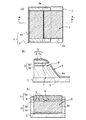
まず、本発明に係る電子放出素子の一例を図1及び図2を用いて説明する。本電子放出素子は、基板1の表面上に積層された絶縁部材3と、基板1との間に絶縁部材3を挟むように、絶縁部材3の上面に設けられたゲート5とを備えている。本例のゲート5は、絶縁部材3上に積層されたゲート5用の導電材料層4と、カソード6用の第一の導電材料層6aとが一体となって構成している。また、絶縁部材3は、順次積層された第一の絶縁材料層3aと第二の絶縁材料層3bとから構成されている。絶縁部材3は、基板1の表面から立ち上がる少なくとも一の側面部を有しており、この絶縁部材3の側面部を構成する第二の絶縁材料層3bの側面部はエッチングにより後退させられて、ゲート5の直下に凹部7が形成されている。また、上記絶縁部材3の側面部を構成する第一の絶縁材料層3aの側面部には、第一の導電材料層6aで形成されたカソード6が設けられている。カソード6の先端部は、凹部7の下縁から上方へ突起し、凹部7の下縁の長さ方向に複数の頂部(ピーク)8が形成された突起部となっている。また、上記頂部8の内側斜面(凹部7の内側に向いた斜面)には、第二の導電材料層6bで形成された副頂部9が設けられている。   First, an example of the electron-emitting device according to the present invention will be described with reference to FIGS. The electron-emitting device includes an insulating member 3 stacked on the surface of the substrate 1 and a gate 5 provided on the upper surface of the insulating member 3 so as to sandwich the insulating member 3 between the substrate 1 and the insulating member 3. . In the gate 5 of this example, the conductive material layer 4 for the gate 5 laminated on the insulating member 3 and the first conductive material layer 6a for the cathode 6 are integrally formed. The insulating member 3 includes a first insulating material layer 3a and a second insulating material layer 3b that are sequentially stacked. The insulating member 3 has at least one side part rising from the surface of the substrate 1, and the side part of the second insulating material layer 3b constituting the side part of the insulating member 3 is retracted by etching, A recess 7 is formed immediately below the gate 5. Further, the cathode 6 formed of the first conductive material layer 6a is provided on the side surface portion of the first insulating material layer 3a constituting the side surface portion of the insulating member 3. The tip of the cathode 6 protrudes upward from the lower edge of the recess 7 and is a protrusion having a plurality of peaks (peaks) 8 formed in the length direction of the lower edge of the recess 7. A sub-top portion 9 formed of the second conductive material layer 6b is provided on the inner slope of the top portion 8 (the slope facing the inner side of the recess 7).

上記電子放出素子は、カソード6とゲート5との間に、ゲート5の電位がカソード6の電位よりも高くなるように電圧を印加することで、カソード6の複数の頂部8と副頂部9とから電子が電界放出される。本発明は、電子放出点として機能する頂部8と共に、この頂部8の内側斜面に更に副頂部9を設けることで電子放出点を増やしているので、アノードへ到達する放出電流を増加させることができる。ゲート5を構成している第一の導電材料層6aと副頂部9との間には、図2(a)に示すように、間隔d′の隙間が形成されている。特に副頂部9の形成は、電子放出点として好ましい間隔d′に制御しやすくし、その結果、電子放出素子の均一性を向上させることができる。   The electron-emitting device applies a voltage between the cathode 6 and the gate 5 such that the potential of the gate 5 is higher than the potential of the cathode 6, thereby providing a plurality of top portions 8 and sub-top portions 9 of the cathode 6. Electrons are emitted from the field. In the present invention, the electron emission point is increased by providing the sub-top part 9 on the inner slope of the top part 8 together with the top part 8 functioning as an electron emission point, so that the emission current reaching the anode can be increased. . A gap d ′ is formed between the first conductive material layer 6a constituting the gate 5 and the sub-top 9 as shown in FIG. In particular, the formation of the sub-top portion 9 can be easily controlled to a distance d ′ preferable as an electron emission point, and as a result, the uniformity of the electron-emitting device can be improved.

なお、ゲート5の配置位置は、図1(a)〜(c)に示す形態に限られるものではない。即ち、電子放出部である複数の頂部8と副頂部9に電界放出可能な電界を印加することができるように、カソード6と所定の間隔を置いて配置されればよい。また、本例におけるゲート5は、ゲート5用の導電材料層4と、カソード6用の第一の導電材料層6aが積層されて構成されているが、導電材料層4単独で構成することもできる。更に、本例における絶縁部材3は、第一の絶縁材料層3aと第二の絶縁材料層3bの積層体で構成されているが、絶縁部材3を一つの絶縁層で構成したり、三つ以上の複数の絶縁層で構成することもできる。   In addition, the arrangement position of the gate 5 is not limited to the form shown in FIGS. That is, the cathode 6 may be arranged at a predetermined interval so that an electric field capable of field emission can be applied to the plurality of top portions 8 and sub-top portions 9 which are electron emission portions. In addition, the gate 5 in this example is configured by laminating the conductive material layer 4 for the gate 5 and the first conductive material layer 6a for the cathode 6, but may be configured by the conductive material layer 4 alone. it can. Furthermore, although the insulating member 3 in this example is composed of a laminate of the first insulating material layer 3a and the second insulating material layer 3b, the insulating member 3 may be composed of one insulating layer, A plurality of insulating layers as described above can also be used.

次に、上記電子放出素子の製造方法における各工程の概要を図3〜図5を用いて説明した後、各工程について詳述する。   Next, the outline of each step in the method for manufacturing the electron-emitting device will be described with reference to FIGS.
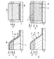
(工程1の概要)
第一の絶縁材料層3aを基板1の表面に形成し、続いて第二の絶縁材料層3bを第一の絶縁材料層3aの上面に積層する。そして、第二の絶縁材料層3bの上面にゲート5となる導電材料層4を積層する〔図3(a)〕。第二の絶縁材料層3bの構成材料は、第一の絶縁材料層3aの材料に比して、後述する工程3で用いるエッチング液(エッチャント)に対するエッチング量が多くなるように、第一の絶縁材料層3aの構成材料とは異なる材料が選択される。
(Outline of process 1)
The first insulating material layer 3a is formed on the surface of the substrate 1, and then the second insulating material layer 3b is laminated on the upper surface of the first insulating material layer 3a. Then, a conductive material layer 4 to be the gate 5 is laminated on the upper surface of the second insulating material layer 3b [FIG. 3 (a)]. The constituent material of the second insulating material layer 3b is such that the amount of etching with respect to an etching solution (etchant) used in step 3 to be described later is larger than that of the first insulating material layer 3a. A material different from the constituent material of the material layer 3a is selected.

(工程2の概要)
次に、導電材料層4、第一の絶縁材料層3a、第二の絶縁材料層3bに対するエッチング処理(第一のエッチング処理)を行う〔図3(b)〕。第一のエッチング処理は、具体的には、フォトリソグラフィー技術等により、導電材料層4上にレジストパターンを形成した後、導電材料層4、第二の絶縁材料層3b、第一の絶縁層3aをエッチングする処理である。この第二のエッチング処理を行う工程2により、上面に導電材料層4が積層され、少なくとも一の側面部を有する絶縁部材3が形成される。なお、図3(b)に示す様に、上記絶縁部材3の側面部を構成する第一の絶縁材料層3aの側面部〔図4(a)に示す第一の導電材料層6aが付設される面〕と、基板1の表面とがなす傾斜角θを90度よりも小さくすることが好ましい。この傾斜角θは、後述するように、50度から60度がより好ましい。更に、上記絶縁部材3の側面部の上方のゲート5の側面部(第一の絶縁材料層3aの上記側面部の上方の面)と、基板1の表面と平行な面とがなす角度を上記傾斜角θよりも小さくすることが好ましい。
(Outline of process 2)
Next, an etching process (first etching process) is performed on the conductive material layer 4, the first insulating material layer 3a, and the second insulating material layer 3b [FIG. 3B]. Specifically, in the first etching process, a resist pattern is formed on the conductive material layer 4 by a photolithography technique or the like, and then the conductive material layer 4, the second insulating material layer 3b, and the first insulating layer 3a. Is a process of etching. By the step 2 of performing the second etching process, the conductive material layer 4 is laminated on the upper surface, and the insulating member 3 having at least one side surface portion is formed. As shown in FIG. 3B, the side surface portion of the first insulating material layer 3a constituting the side surface portion of the insulating member 3 [the first conductive material layer 6a shown in FIG. The inclination angle θ formed by the surface of the substrate 1 and the surface of the substrate 1 is preferably smaller than 90 degrees. The inclination angle θ is more preferably 50 to 60 degrees as will be described later. Furthermore, the angle formed by the side surface portion of the gate 5 above the side surface portion of the insulating member 3 (the surface above the side surface portion of the first insulating material layer 3a) and the surface parallel to the surface of the substrate 1 is as described above. It is preferable to make it smaller than the inclination angle θ.

(工程3の概要)
続いて、第二の絶縁材料層3bに対するエッチング処理(第二のエッチング処理)を行う〔図3(c)〕。第二のエッチング処理は、第二の絶縁材料層3bを選択的にエッチングする処理である。この第二のエッチング処理を行う工程3により、第二の絶縁材料層3bの側面部が後退し、前記絶縁部材3の側面部における導電材料層4直下に、第一絶縁材料層3aと導電材料層4に挟まれた状態の凹部7が形成される。この工程3により、第一の絶縁材料層3aの上面部の一部が凹部7内に露出する。この露出した第一の絶縁材料層3aの上面部の一部と、第一の絶縁材料層3aの前記側面部との間のコーナー部が凹部7の下縁である。
(Outline of process 3)
Subsequently, an etching process (second etching process) is performed on the second insulating material layer 3b [FIG. 3C]. The second etching process is a process of selectively etching the second insulating material layer 3b. By the step 3 in which the second etching process is performed, the side surface portion of the second insulating material layer 3b is retreated, and the first insulating material layer 3a and the conductive material are directly below the conductive material layer 4 in the side surface portion of the insulating member 3. A recess 7 sandwiched between the layers 4 is formed. By this step 3, a part of the upper surface portion of the first insulating material layer 3 a is exposed in the recess 7. A corner portion between the part of the exposed upper surface portion of the first insulating material layer 3 a and the side surface portion of the first insulating material layer 3 a is the lower edge of the recess 7.

(工程4の概要)
第一の導電材料層6aをスパッタリング法により堆積させる〔図4(a)〕。第一の導電材料層6aの堆積は、全圧が1.0Pa以下の条件下で、スパッタリング法により行われる。この全圧下で成膜することで、後述する工程5のエッチングによって、有意な頂部8〔図4(b)参照〕を形成するのに適した第一の導電材料層6aを形成することができる。また、後述する工程7のエッチングに耐える第一の導電材料層6aとすることができる。第一の導電材料層6aは、第一の絶縁材料層3aの側面部から、凹部7内に露出した第一の絶縁材料層3aの上面にかけて延在するように成膜されると共に、凹部7の下縁から上方へ突起した突起部を形成する。同時に、導電材料層4上及び基板1の表面上にも堆積する。本例において導電材料層4上の第一の導電材料層6aは、導電材料層4と一体となってゲート5を構成する。図4(a)には、第一の絶縁材料層3aの側面部側の第一の導電材料層6aと、導電材料層4上の第一の導電材料層6aとが、凹部7部分で離れて接触しないように成膜した例を示している。しかし、両者が接触するように成膜する場合もある。
(Outline of process 4)
The first conductive material layer 6a is deposited by sputtering [FIG. 4 (a)]. The deposition of the first conductive material layer 6a is performed by a sputtering method under the condition that the total pressure is 1.0 Pa or less. By forming the film under this total pressure, the first conductive material layer 6a suitable for forming a significant top 8 [see FIG. 4B] can be formed by etching in step 5 described later. . Moreover, it can be set as the 1st conductive material layer 6a which can endure the etching of the process 7 mentioned later. The first conductive material layer 6a is formed so as to extend from the side surface portion of the first insulating material layer 3a to the upper surface of the first insulating material layer 3a exposed in the concave portion 7, and the concave portion 7 is also formed. Protrusions projecting upward from the lower edge are formed. At the same time, it is also deposited on the conductive material layer 4 and the surface of the substrate 1. In this example, the first conductive material layer 6 a on the conductive material layer 4 is integrated with the conductive material layer 4 to form the gate 5. In FIG. 4A, the first conductive material layer 6a on the side surface side of the first insulating material layer 3a and the first conductive material layer 6a on the conductive material layer 4 are separated at the recess 7 portion. In this example, the film is formed so as not to come into contact. However, the film may be formed so that both are in contact with each other.

(工程5の概要)
続いて、少なくとも第一の導電材料層6aに対してエッチング処理(第三のエッチング処理)を行い、カソード6を形成する〔図4(b)〕。第三のエッチング処理は、電子放出部である複数の頂部8を形成することを主眼とした処理である。この第三のエッチング処理では第一の導電材料層6aの露出している表面全てが、エッチング液に曝されることになる。なお、工程4で第一の絶縁材料層3aの側面部側の第一の導電材料層6aと、導電材料層4上の第一の導電材料層6aとを接触するように成膜した場合には、本工程で両者間に間隙を形成する。また、工程4で第一の絶縁材料層3aの側面部側の第一の導電材料層6aと、導電材料層4上の第一の導電材料層6aとを接触しないように成膜した場合には、本工程で両者間の間隔dが広げられる。工程5により、図4(b)に示すように、凹部7の下縁から上に向かって突起した突起部に、凹部7の下縁の長さ方向に沿って複数の頂部8が形成される。また、工程5により、凹部7内に付着している余計な第一の導電材料層6aの構成材料を除去することもできる。
(Outline of process 5)
Subsequently, at least the first conductive material layer 6a is subjected to an etching process (third etching process) to form the cathode 6 (FIG. 4B). The third etching process is a process whose main purpose is to form a plurality of top portions 8 which are electron emission portions. In the third etching process, the entire exposed surface of the first conductive material layer 6a is exposed to the etching solution. In Step 4, when the first conductive material layer 6a on the side surface side of the first insulating material layer 3a and the first conductive material layer 6a on the conductive material layer 4 are formed so as to be in contact with each other. In this step, a gap is formed between the two. Further, when the first conductive material layer 6a on the side surface side of the first insulating material layer 3a and the first conductive material layer 6a on the conductive material layer 4 are formed in step 4 so as not to contact each other. In this step, the distance d between the two is widened. In step 5, as shown in FIG. 4B, a plurality of top portions 8 are formed along the length direction of the lower edge of the recess 7 in the protrusion protruding upward from the lower edge of the recess 7. . Further, in step 5, the extra constituent material of the first conductive material layer 6a adhering in the recess 7 can be removed.

(工程6の概要)
カソード6上から、少なくともその突起部を覆って第二の導電材料層6bを堆積する〔図5(a)〕。この第二の導電材料層6bの形成は、詳しくは後述するが、全圧が1.0Pa以上2.8Pa以下の条件下で、スパッタリング法により行う。この条件で成膜することで、後述する工程7におけるエッチングによって有意な副頂部9〔図5(b)参照〕を形成するのに適した第二の導電材料層6bを形成できる。第二の導電材料層6bは、第一の絶縁材料層3aの側面部上のカソード6部分から、凹部7の下縁から突起した突起部にかけて延在するように成膜されると共に、ゲート5上に成膜される。図5(a)には、カソード6側の第二の導電材料層6bと、ゲート5側の第二の導電材料層6bとが接触するように成膜した例を示しているが、両者が接触しないように成膜する場合もある。
(Outline of process 6)
A second conductive material layer 6b is deposited from above the cathode 6 so as to cover at least the projections (FIG. 5A). Although the formation of the second conductive material layer 6b will be described later in detail, the second conductive material layer 6b is formed by a sputtering method under a condition where the total pressure is 1.0 Pa or more and 2.8 Pa or less. By forming the film under these conditions, it is possible to form the second conductive material layer 6b suitable for forming a significant sub-top 9 [see FIG. 5B] by etching in step 7 described later. The second conductive material layer 6b is formed so as to extend from the cathode 6 portion on the side surface portion of the first insulating material layer 3a to the protruding portion protruding from the lower edge of the recess 7, and the gate 5 A film is formed on top. FIG. 5A shows an example in which the second conductive material layer 6b on the cathode 6 side and the second conductive material layer 6b on the gate 5 side are in contact with each other. In some cases, the film is formed so as not to contact.

(工程7の概要)
続いて、第二の導電材料層6bに対してエッチング処理(第四のエッチング処理)を行い、副頂部9を形成する〔図5(b)〕。全圧が1.0Pa以上2.8Pa以下の条件下でスパッタリング法により形成された第二の導電材料層6bは、工程4で1.0Pa以下の条件下でスパッタリング法により形成された第一の導電材料層6aよりもエッチング液への溶解性が大きい。エッチング処理後、第二の導電材料層6bの大部分が溶解除去されても、第一の導電材料層6aは大きくエッチングされることなく、カソード6として残すことができる。特にカソード6の先端部分に形成されている頂部8はゲート5との間に狭い隙間を形成する。カソード6の先端部分に形成された突起部とゲート5間の隙間のうち、頂部8とゲート5との間の隙間は他の隙間より狭く、頂部8の内側斜面の第二の導電材料層6bはエッチング処理で溶解しにくく、結果として残留して副頂部9を形成する。
(Outline of process 7)
Subsequently, an etching process (fourth etching process) is performed on the second conductive material layer 6b to form the sub-top portion 9 [FIG. 5B]. The second conductive material layer 6b formed by the sputtering method under the condition where the total pressure is 1.0 Pa or more and 2.8 Pa or less is the first conductive material layer 6b formed by the sputtering method under the condition of 1.0 Pa or less in Step 4. It is more soluble in the etching solution than the conductive material layer 6a. Even after most of the second conductive material layer 6b is dissolved and removed after the etching process, the first conductive material layer 6a can be left as the cathode 6 without being largely etched. In particular, the top 8 formed at the tip of the cathode 6 forms a narrow gap with the gate 5. Among the gaps between the protrusions formed at the tip of the cathode 6 and the gate 5, the gap between the top 8 and the gate 5 is narrower than the other gaps, and the second conductive material layer 6 b on the inner slope of the top 8. Is difficult to dissolve in the etching process, and as a result, it remains to form the sub-top 9.

基本的には、以上の工程1〜工程7により、図1に示した電子放出素子を製造することができる。以下、各工程について詳細に説明する。   Basically, the electron-emitting device shown in FIG. 1 can be manufactured by the steps 1 to 7 described above. Hereinafter, each step will be described in detail.

(工程1の詳細)
工程1は、概要を図3(a)で説明した積層工程である。基板1は、電子放出素子を支持するためのベースである。石英ガラス,Na等の不純物含有量を減少させたガラス、青板ガラス等を用いることができる。基板1に必要な機能としては、機械的強度が高いだけでなく、ドライエッチング、ウェットエッチング、現像液等のアルカリや酸に対して耐性があることが挙げられる。また、画像表示装置に用いる場合は、加熱工程等を経るので、積層する部材との熱膨張率の差が小さいものが好ましい。また、処理を考慮すると、ガラス内部からのアルカリ元素等が電子放出素子に拡散しづらい材料が好ましい。
(Details of process 1)
Step 1 is the stacking step whose outline has been described with reference to FIG. The substrate 1 is a base for supporting the electron-emitting device. Quartz glass, glass with reduced impurity content such as Na, blue plate glass, and the like can be used. Functions necessary for the substrate 1 include not only high mechanical strength but also resistance to alkalis and acids such as dry etching, wet etching, and developer. Moreover, when using for an image display apparatus, since a heating process etc. are passed, the thing with a small difference of a thermal expansion coefficient with the member to laminate | stack is preferable. In consideration of the treatment, a material in which an alkali element or the like from the inside of the glass is difficult to diffuse into the electron-emitting device is preferable.

第一の絶縁材料層3aと第二の絶縁材料層3bを構成する材料は、加工性に優れる材料からなり、例えば窒化シリコン(典型的にはSi34)や酸化シリコン(典型的にはSiO2)を用いることができる。第一の絶縁材料層3aと第二の絶縁材料層3bは、スパッタリング法等の一般的な真空成膜法、CVD法、真空蒸着法で形成することができる。また、第一の絶縁材料層3aの厚さは、数nmから数十μmの範囲で設定され、好ましくは数十nmから数百nmの範囲に選択される。第二の絶縁材料層3bの厚さは、第一の絶縁材料層3aよりも薄く、数nmから数百nmの範囲で設定され、好ましくは数nmから数十nmの範囲で選択される。 The material constituting the first insulating material layer 3a and the second insulating material layer 3b is made of a material excellent in workability, for example, silicon nitride (typically Si 3 N 4 ) or silicon oxide (typically SiO 2 ) can be used. The first insulating material layer 3a and the second insulating material layer 3b can be formed by a general vacuum film forming method such as a sputtering method, a CVD method, or a vacuum evaporation method. The thickness of the first insulating material layer 3a is set in the range of several nm to several tens of μm, and is preferably selected in the range of several tens of nm to several hundreds of nm. The thickness of the second insulating material layer 3b is thinner than the first insulating material layer 3a, is set in the range of several nm to several hundred nm, and is preferably selected in the range of several nm to several tens of nm.

第一の絶縁材料層3aと第二の絶縁材料層3bを基板1上に積層した後に工程3にて凹部7を形成する場合は、上記第二のエッチング処理に対して、第一の絶縁材料層3aよりも第二の絶縁材料層3bの方がよりエッチング量が多い関係に設定する。望ましくは、第一の絶縁材料層3aと第二の絶縁材料層3bとの間のエッチング量の比は、10以上であることが好ましく、50以上であることが更に好ましい。このようなエッチング量の比を得るためには、例えば、第一の絶縁材料層3aを窒化シリコン膜で形成し、第二の絶縁材料層3bを酸化シリコン膜やリン濃度の高いPSGやホウ素濃度の高いBSG膜等で構成すれば良い。なお、PSGはリンシリケートガラスであり、BSGはボロンシリケートガラスである。   When the recess 7 is formed in step 3 after laminating the first insulating material layer 3a and the second insulating material layer 3b on the substrate 1, the first insulating material is used for the second etching process. The second insulating material layer 3b is set to have a larger etching amount than the layer 3a. Desirably, the ratio of the etching amount between the first insulating material layer 3a and the second insulating material layer 3b is preferably 10 or more, and more preferably 50 or more. In order to obtain such a ratio of etching amounts, for example, the first insulating material layer 3a is formed of a silicon nitride film, and the second insulating material layer 3b is formed of a silicon oxide film, a high phosphorus concentration of PSG, or a boron concentration. A high BSG film or the like may be used. Note that PSG is phosphorus silicate glass and BSG is boron silicate glass.

ゲート5を構成する導電材料層4は導電性を有しており、蒸着法、スパッタリング法等の一般的真空成膜技術により形成されるものである。導電材料層4の構成材料は、導電性に加えて高い熱伝導率があり、融点が高い材料が望ましい。例えば、Be,Mg,Ti,Zr,Hf,V,Nb,Ta,Mo,W,Al,Cu,Ni,Cr,Au,Pt,Pd等の金属又はこれらの合金材料が使用できる。炭化物や硼化物や窒化物も使用できる。また、導電材料層4の厚さは、数nmから数百nmの範囲で設定され、好ましくは数十nmから数百nmの範囲で選択される。   The conductive material layer 4 constituting the gate 5 has conductivity, and is formed by a general vacuum film forming technique such as vapor deposition or sputtering. The constituent material of the conductive material layer 4 is preferably a material having high thermal conductivity and high melting point in addition to conductivity. For example, metals such as Be, Mg, Ti, Zr, Hf, V, Nb, Ta, Mo, W, Al, Cu, Ni, Cr, Au, Pt, and Pd, or alloy materials thereof can be used. Carbides, borides and nitrides can also be used. The thickness of the conductive material layer 4 is set in the range of several nm to several hundred nm, and preferably selected in the range of several tens nm to several hundred nm.

(工程2の詳細)
工程2は、概要を図3(b)で説明した第一のエッチング処理を施す工程である。第一のエッチング処理では、エッチングガスをプラズマ化して材料に照射することで材料の精密なエッチング加工が可能な、RIE(Reactive Ion Etching)を用いることが好ましい。RIEに用いるガスとしては、加工する対象部材がフッ化物を作る材料である場合には、CF4やCHF3やSF6等のフッ素系ガスが選ばれる。加工する対象部材がSiやAlのような塩化物を形成する材料である場合には、Cl2、BCl3等の塩素系ガスが選ばれる。また、レジストとの選択比を取るためや、エッチング面の平滑性の確保、更にはエッチングスピードを上げるため、水素、酸素、アルゴンガスの少なくともいずれかをエッチングガスに添加することが好ましい。
(Details of process 2)
Step 2 is a step of performing the first etching process whose outline has been described with reference to FIG. In the first etching process, it is preferable to use RIE (Reactive Ion Etching), in which a material can be precisely etched by irradiating the material with an etching gas. As the gas used for RIE, a fluorine-based gas such as CF 4 , CHF 3, or SF 6 is selected when the target member to be processed is a material that produces fluoride. When the target member to be processed is a material that forms a chloride such as Si or Al, a chlorine-based gas such as Cl 2 or BCl 3 is selected. Further, it is preferable to add at least one of hydrogen, oxygen, and argon gas to the etching gas in order to obtain a selection ratio with the resist, to ensure the smoothness of the etching surface, and to increase the etching speed.

工程2により、図1に示した絶縁部材3及びゲート5の基本形状が形成される。但し、工程3以降で行われる各種のエッチング処理で、絶縁部材3及びゲート5を構成する導電材料層4が全くエッチングされないことを意味する訳ではない。   In step 2, the basic shapes of the insulating member 3 and the gate 5 shown in FIG. 1 are formed. However, it does not mean that the insulating material 3 and the conductive material layer 4 constituting the gate 5 are not etched at all by various etching processes performed in the process 3 and subsequent steps.

絶縁部材3の側面部を構成する第一の絶縁材料層3aの側面部の傾斜角θ(該側面部と基板1の表面とがなす角度)は、ガス種、圧力等の条件を制御することで所望の値に制御可能である。θは、90度よりも小さい角度とすることが好ましい。θを90度よりも小さい角度に設定することで、結果として導電材料層4の側面部を第一の絶縁材料層3aの側面部よりも後退させることができる。また、導電材料層4の側面部の傾斜角(該側面部と基板1の表面と平行な面とがなす角度)を、第一の絶縁材料層3aの側面部の傾斜角θよりも小さくすることが好ましい。なお、θは、絶縁部材3の側面部において、第一の絶縁材料層3aと第二の絶縁材料層3bとの境界部から基板1方向へ接線を引いたときに、この接線と基板1の表面とがなす角度で表すことができる。   The inclination angle θ (angle formed by the side surface portion and the surface of the substrate 1) of the side surface portion of the first insulating material layer 3a constituting the side surface portion of the insulating member 3 controls conditions such as gas type and pressure. Can be controlled to a desired value. θ is preferably an angle smaller than 90 degrees. By setting θ to an angle smaller than 90 degrees, as a result, the side surface portion of the conductive material layer 4 can be made to recede from the side surface portion of the first insulating material layer 3a. Further, the inclination angle of the side surface portion of the conductive material layer 4 (angle formed by the side surface portion and a surface parallel to the surface of the substrate 1) is made smaller than the inclination angle θ of the side surface portion of the first insulating material layer 3a. It is preferable. In addition, when θ is drawn from the boundary between the first insulating material layer 3a and the second insulating material layer 3b toward the substrate 1 in the side surface portion of the insulating member 3, the tangent and the substrate 1 It can be expressed by the angle formed by the surface.

(工程3の詳細)
工程3は、概要を図3(c)で説明した第二のエッチング処理を施す工程である。工程3のエッチング液は、第二の絶縁材料層3bがエッチングされる量に対して、第一の絶縁材料層3aのエッチングされる量が十分に低くなるように選択される。第二のエッチング処理は、例えば第二の絶縁材料層3bが酸化シリコンで形成され、第一の絶縁材料層3aが窒化シリコンで形成されている場合、エッチング液としてバッファードフッ酸(BHF)を用いればよい。BHFはフッ化アンモニウムとフッ酸との混合溶液である。また、第二の絶縁材料層3bが窒化シリコンで形成され、第一の絶縁材料層3aが酸化シリコンで形成されている場合、エッチング液は熱リン酸系エッチング液を使用すればよい。この工程3により、図1に示した凹部7を備えたパターンが形成される。しかしながら、工程3以降に行われるエッチング処理で、第二の絶縁材料層3bが全くエッチングされないことを意味する訳ではない。
(Details of process 3)
Step 3 is a step of performing the second etching process whose outline has been described with reference to FIG. The etching solution in step 3 is selected so that the amount of etching of the first insulating material layer 3a is sufficiently lower than the amount of etching of the second insulating material layer 3b. In the second etching process, for example, when the second insulating material layer 3b is formed of silicon oxide and the first insulating material layer 3a is formed of silicon nitride, buffered hydrofluoric acid (BHF) is used as an etching solution. Use it. BHF is a mixed solution of ammonium fluoride and hydrofluoric acid. Further, when the second insulating material layer 3b is formed of silicon nitride and the first insulating material layer 3a is formed of silicon oxide, a hot phosphoric acid-based etching solution may be used. By this step 3, a pattern having the recesses 7 shown in FIG. 1 is formed. However, this does not mean that the second insulating material layer 3b is not etched at all in the etching process performed after the step 3.

凹部7の深さ(奥行き方向の距離)は、電子放出素子のリーク電流に深く関わる。凹部7を深く形成するほどリーク電流の値は小さくなる。しかし、あまり凹部7を深くするとゲート5が変形する等の問題が発生する。このため、凹部7の深さは実用的には30nm以上200nm以下に設定される。なお、凹部7の深さは、凹部7の下縁である第一の絶縁材料層3aの端部から、第二の絶縁材料層3bの後退した側面部までの距離と言い換えることもできる。凹部7の下縁である第一の絶縁材料層3aの側面部と上面部間は、角で接続された形態に限定されるものではなく、所定の曲率をもって接続された形態でもよい。   The depth (distance in the depth direction) of the recess 7 is deeply related to the leakage current of the electron-emitting device. The deeper the recess 7, the smaller the leak current value. However, if the recess 7 is made too deep, problems such as deformation of the gate 5 occur. For this reason, the depth of the recess 7 is practically set to 30 nm or more and 200 nm or less. In addition, the depth of the recessed part 7 can also be called the distance from the edge part of the 1st insulating material layer 3a which is the lower edge of the recessed part 7 to the side part which the 2nd insulating material layer 3b retreated. The shape between the side surface portion and the upper surface portion of the first insulating material layer 3a, which is the lower edge of the concave portion 7, is not limited to the form connected at the corners, but may be the form connected with a predetermined curvature.

(工程4の詳細)
工程4は、概要を図4(a)で説明した第一の導電材料層6aを形成する工程である。第一の導電材料層6aは、カソード6を構成する材料をスパッタリング法により成膜することで形成される。第一の導電材料層6aの構成材料は、導電性があり、電子を電界放出することのできる材料であればよく、好ましくは、2000℃以上の高融点の材料から選択される。また、第一の導電材料層6aの構成材料は、5eV以下の仕事関数材料であり、その酸化物が簡易にエッチング可能な材料であることが好ましい。このような材料の好適な例として、例えば、Hf,V,Nb,Ta,Mo,W,Au,Pt,Pd等の金属又はこれらの合金材料が挙げられる。工程5においてエッチング処理を行うことを考慮すると、第一の導電材料層6aの構成材料としては、Mo又はWを用いることが特に好ましい。
(Details of step 4)
Step 4 is a step of forming the first conductive material layer 6a whose outline has been described with reference to FIG. The first conductive material layer 6a is formed by depositing the material constituting the cathode 6 by sputtering. The constituent material of the first conductive material layer 6a may be any material that is conductive and capable of field emission of electrons, and is preferably selected from materials having a high melting point of 2000 ° C. or higher. The constituent material of the first conductive material layer 6a is a work function material of 5 eV or less, and the oxide is preferably a material that can be easily etched. Suitable examples of such materials include metals such as Hf, V, Nb, Ta, Mo, W, Au, Pt, and Pd, or alloy materials thereof. In consideration of performing the etching process in step 5, it is particularly preferable to use Mo or W as the constituent material of the first conductive material layer 6a.

第一の導電材料層6aの構成材料のスパッタリング法による成膜は、2.8Pa以下の全圧下で行う。特に、第一の導電材料層6aは、次の工程のエッチングで頂部8〔図4(b)参照〕を形成する時、更に工程7のエッチングで副頂部9〔図5(b)参照〕を形成する時、エッチング液に曝されても、カソード6としてエッチング液に耐え残る安定な膜であることが必要である。このため、第一の導電材料層6aとしては、1.0Pa以下の全圧下でスパッタリングを行って得られる、膜密度が高い(結晶粒部分が多い)膜を用いる。   Film formation of the constituent material of the first conductive material layer 6a by the sputtering method is performed under a total pressure of 2.8 Pa or less. In particular, when the first conductive material layer 6a forms the top portion 8 [see FIG. 4B] by etching in the next step, the sub-top portion 9 [see FIG. 5B] is further etched in step 7. When forming, the cathode 6 needs to be a stable film that can withstand the etching solution even when exposed to the etching solution. For this reason, as the first conductive material layer 6a, a film having a high film density (a large number of crystal grain portions) obtained by performing sputtering under a total pressure of 1.0 Pa or less is used.

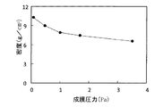
スパッタ時の全圧が膜質及びエッチング特性へ与える影響について説明する。図6に示すように、スパッタ時の全圧を変化させて導電性膜の成膜を行ったところ、1.0Paを境に、膜密度の減少率が急激に低下することがわかった。このように、1.0Paよりも低い圧力下で成膜した場合は得られる導電性膜の膜密度が高く(結晶粒部分が多くなる)、1.0Paよりも高い圧力下で成膜した場合は導電性膜の膜密度が低くなる(結晶粒界部分が多くなる)。図7に導電性の膜における結晶粒部分と結晶粒界部分についての模式図を示す。結晶粒部分と結晶粒界部分との間にはエッチングの選択比がある。このため、導電性の膜に対して工程5のエッチング処理を行うと、結晶粒界部分が結晶粒部分に比べて優先的にエッチングされると考えられる。この結果、図8に示すように、スパッタ時の全圧の差で、エッチング処理のレート(エッチングレート)に大きな差が生じる。グラフの中でA−1で示す曲線は1.7Paの全圧下で成膜した導電性膜の場合を示し、B−1で示す曲線は、0.1Paの全圧下で成膜した導電性膜の場合を示す。成膜圧力が低いときはエッチングレートが遅く、高いときはエッチングレートが速い。この結果はエッチング処理をTMAH(水酸化テトラメチルアンモニウム)の0.3wt%濃度のエッチング液(40℃)で行ったときのものである。   The influence of the total pressure during sputtering on the film quality and etching characteristics will be described. As shown in FIG. 6, when the conductive film was formed by changing the total pressure at the time of sputtering, it was found that the rate of decrease in the film density suddenly decreased at 1.0 Pa. As described above, when the film is formed under a pressure lower than 1.0 Pa, the obtained conductive film has a high film density (the number of crystal grains increases), and when the film is formed under a pressure higher than 1.0 Pa. Decreases the density of the conductive film (the number of crystal grain boundaries increases). FIG. 7 shows a schematic diagram of crystal grain portions and crystal grain boundary portions in a conductive film. There is an etching selectivity between the crystal grain part and the crystal grain boundary part. For this reason, it is considered that when the conductive film is subjected to the etching process in step 5, the crystal grain boundary portion is preferentially etched as compared with the crystal grain portion. As a result, as shown in FIG. 8, there is a large difference in the etching process rate (etching rate) due to the difference in total pressure during sputtering. In the graph, the curve indicated by A-1 indicates the case of a conductive film formed under a total pressure of 1.7 Pa, and the curve indicated by B-1 indicates a conductive film formed under a total pressure of 0.1 Pa. This case is shown. When the deposition pressure is low, the etching rate is slow, and when it is high, the etching rate is fast. This result is obtained when the etching treatment is performed with an etching solution (40 ° C.) of TMAH (tetramethylammonium hydroxide) having a concentration of 0.3 wt%.

図9はスパッタリング時の全圧を変えた時に、エッチング時間の経過による間隔d〔図4(b)参照〕の変化を示すグラフである。この間隔dは、カソード6(カソード6を構成する第一の導電材料層6a)とゲート5(ゲート5の上層を構成する第一の導電材料層6a)間の隙間の距離である。横軸はエッチング時間を表しており、縦軸はカソード6とゲート5との間の間隔dの標準偏差σを表している。図9において、A−2で示す曲線は、第一の導電材料層6aを1.7Paの全圧下で成膜した場合を示しており、全圧が1.0Pa以上2.8Pa以下の範囲ではこのA−2と似通った曲線となる。A−3で示す曲線は、第一の導電材料層6aを3.0Paの全圧下で成膜した場合を示しており、全圧が2.8Paよりも高い範囲ではこのA−3と似通った曲線となる。B−2で示す曲線は、第一の導電材料層6aを0.1Paの全圧下で成膜した場合を示しており、全圧が1.0Paよりも低い範囲ではこのB−2と似通った曲線となる。図7からすると、A−2で代表される、全圧が1.0Pa以上2.8Pa以下の圧力範囲で成膜した場合、エッチング時間によってはこの圧力範囲とは異なる圧力で成膜した場合に比べて大きなσになる。A−3で代表される、2.8Pa以上の大きな全圧下で成膜した場合は、σの変化がエッチング時間に対してより敏感になり、上述した他の圧力範囲で成膜した場合に比べて、制御性が劣る傾向が顕著になる。これは、上述した圧力範囲で成膜した場合に比べて、結晶粒界部分が多く形成されるためと考えられ、また得られるσの最大値も、上述した圧力範囲で成膜した場合に比べて小さな値となる。   FIG. 9 is a graph showing changes in the distance d (see FIG. 4B) with the lapse of etching time when the total pressure during sputtering is changed. This distance d is the distance between the cathode 6 (first conductive material layer 6a constituting the cathode 6) and the gate 5 (first conductive material layer 6a constituting the upper layer of the gate 5). The horizontal axis represents the etching time, and the vertical axis represents the standard deviation σ of the distance d between the cathode 6 and the gate 5. In FIG. 9, the curve indicated by A-2 shows the case where the first conductive material layer 6a is formed under a total pressure of 1.7 Pa. In the range where the total pressure is 1.0 Pa or more and 2.8 Pa or less. It becomes a curve similar to this A-2. A curve indicated by A-3 shows a case where the first conductive material layer 6a is formed under a total pressure of 3.0 Pa, and is similar to A-3 in a range where the total pressure is higher than 2.8 Pa. It becomes a curve. The curve indicated by B-2 shows a case where the first conductive material layer 6a is formed under a total pressure of 0.1 Pa, and is similar to B-2 in a range where the total pressure is lower than 1.0 Pa. It becomes a curve. According to FIG. 7, when the film is formed in a pressure range represented by A-2 and the total pressure is 1.0 Pa or more and 2.8 Pa or less, depending on the etching time, the film is formed at a pressure different from this pressure range. Compared to a large σ. When the film is formed under a large total pressure of 2.8 Pa or more, represented by A-3, the change in σ becomes more sensitive to the etching time, compared with the case where the film is formed in the other pressure range described above. Thus, the tendency of poor controllability becomes remarkable. This is considered to be because more crystal grain boundaries are formed compared to the case where the film is formed in the pressure range described above, and the maximum value of σ obtained is also higher than that in the case where the film is formed within the pressure range described above. And a small value.

一方、B−2で代表される、1.0Paよりも小さな全圧下で成膜した場合は、工程5のエッチング時間を増やしても、σはほとんど変化しない傾向が顕著になる。これは、上述した他の圧力範囲で成膜した場合に比べて、結晶粒部分が多く形成されるためである。結晶粒部分と結晶粒界部分の差は、金属と金属酸化物の差を意味する。Moを例に挙げると、結晶粒部分に金属的なMoが存在している。一方、結晶粒界部分ではMoOx、MoO2等のMo酸化物が混在しており、特に最表面でMoO3が局在化している。TMAH等のアルカリ水溶液をエッチング液として用いた場合、Mo酸化物がエッチングされやすい。金属Moは、液中の溶存酸素により酸化が進まない限り、容易にエッチングが進まない。よって、カソード6を構成する第一の導電材料層6aとして好ましいのは、1.0Pa以下の圧力下でスパッタリングされた導電性膜であり、この膜はエッチング液に耐えて残る安定な膜である。しかし、第一の導電材料層6aのもうひとつの機能である複数の頂部8を形成する目的に対して、1.0Pa以下の圧力下でスパッタリングされた導電性膜は、頂部8を形成する有意なエッチングが実質的に行われない。この課題への対処は、後述するエッチング工程で説明する。 On the other hand, when the film is formed under a total pressure smaller than 1.0 Pa, represented by B-2, the tendency that σ hardly changes even when the etching time in step 5 is increased becomes significant. This is because more crystal grain portions are formed than in the case where the film is formed in the other pressure range described above. The difference between the crystal grain part and the crystal grain boundary part means a difference between the metal and the metal oxide. Taking Mo as an example, metallic Mo exists in the crystal grain portion. On the other hand, in the grain boundary portion MoOx, and Mo oxide such as MoO 2 are mixed, the MoO 3 in particular the outermost surface is localized. When an alkaline aqueous solution such as TMAH is used as an etchant, the Mo oxide is easily etched. Etching of the metal Mo does not proceed easily unless the oxidation proceeds due to dissolved oxygen in the liquid. Accordingly, the first conductive material layer 6a constituting the cathode 6 is preferably a conductive film sputtered under a pressure of 1.0 Pa or less, and this film is a stable film that can withstand etching liquid. . However, for the purpose of forming the plurality of top portions 8 which is another function of the first conductive material layer 6 a, the conductive film sputtered under a pressure of 1.0 Pa or less is significant in forming the top portions 8. Etching is substantially not performed. The coping with this problem will be described in the etching process described later.

導電性膜の密度や組成の測定は、一般にはXRR、XPS等が用いられるが、実際の電子放出素子では測定が困難な場合がある。そのような場合には、密度や組成の測定手法として、例えば以下の方法を採用することができる。即ち、TEM(透過電子顕微鏡)とEELS(電子エネルギー損失分光)を組み合わせた高分解能電子エネルギー損失分光電子顕微鏡で元素の定量分析を行い、密度や組成を算出することができる。また、カソード6とゲート5側の第一の導電材料層6aとの間隔dの標準偏差σは、例えばSEMにて、カソード6とゲート5との間の隙間の長さ方向に沿って順次間隔dを測定し、測定した複数のdから算出することができる。スパッタ時の全圧が導電性膜の膜質、エッチング特性へ与える影響については、第一の導電材料層6aとして好適な導電性膜であれば同様の傾向を示す。また、スパッタリング時のパワーや、基板1とスパッタターゲットとの距離等が一般的な範囲であれば、特段の依存性は見られない。   In general, XRR, XPS, or the like is used to measure the density and composition of the conductive film, but it may be difficult to measure with an actual electron-emitting device. In such a case, for example, the following method can be adopted as a method for measuring density and composition. That is, the element can be quantitatively analyzed with a high-resolution electron energy loss spectroscopic electron microscope combining TEM (transmission electron microscope) and EELS (electron energy loss spectroscopy), and the density and composition can be calculated. The standard deviation σ of the distance d between the cathode 6 and the first conductive material layer 6a on the gate 5 side is, for example, in SEM, sequentially along the length direction of the gap between the cathode 6 and the gate 5 d can be measured and calculated from a plurality of measured d. About the influence which the total pressure at the time of sputtering has on the film quality and etching characteristics of the conductive film, the same tendency is shown as long as the conductive film is suitable as the first conductive material layer 6a. In addition, if the power during sputtering, the distance between the substrate 1 and the sputtering target, and the like are in a general range, no particular dependency is observed.

スパッタガスとしては、アルゴン(Ar)ガス、クリプトン(Kr)ガス、キセノン(Xe)ガス等を用いることができるが、特にアルゴンガスが製造コストの面から好ましい。スパッタ電源としては、DC電源、13.56MHz等の工業用電源周波数のRF電源が使用できる。スパッタリング時のパワーは、放電電力をターゲットの面積で除した値であり、一般的範囲としては、例えば、1W/cm2以上5W/cm2以下とすることができる。また、スパッタターゲットと基板1との距離は、一般的範囲としては、例えば50mm以上200mm以下とすることができる。 As a sputtering gas, argon (Ar) gas, krypton (Kr) gas, xenon (Xe) gas, or the like can be used, and argon gas is particularly preferable from the viewpoint of manufacturing cost. As the sputtering power source, a DC power source, an RF power source with an industrial power source frequency such as 13.56 MHz can be used. The power at the time of sputtering is a value obtained by dividing the discharge power by the area of the target, and the general range can be, for example, 1 W / cm 2 or more and 5 W / cm 2 or less. Moreover, the distance between the sputtering target and the substrate 1 can be set to, for example, 50 mm or more and 200 mm or less as a general range.

カソード6を構成する第一の導電材料層6aとゲート5の上層を構成する第一の導電材料層6aは、同一材料でも良いし、異なる材料でも良い。しかしながら、製造の容易性、エッチングの制御性から、カソード6を構成する第一の導電材料層6aとゲート5の上層を構成する第一の導電材料層6aは同一材料で同時に成膜することが好ましい。これらの膜厚は、10nmから40nmの範囲で設定され、好ましくは15nmから30nmの範囲で選択される。また、本工程では、カソード6を構成する第一の導電材料層6aとゲート5の上層を構成する第一の導電材料層6aとを接触させて形成しても良いし、接触せずに形成しても良い。接触させて形成した場合には、工程5によって、両者間に隙間を形成することができる。   The first conductive material layer 6a constituting the cathode 6 and the first conductive material layer 6a constituting the upper layer of the gate 5 may be the same material or different materials. However, the first conductive material layer 6a constituting the cathode 6 and the first conductive material layer 6a constituting the upper layer of the gate 5 can be simultaneously formed of the same material because of ease of manufacture and controllability of etching. preferable. These film thicknesses are set in the range of 10 nm to 40 nm, and preferably selected in the range of 15 nm to 30 nm. In this step, the first conductive material layer 6a constituting the cathode 6 and the first conductive material layer 6a constituting the upper layer of the gate 5 may be formed in contact with each other, or formed without contact. You may do it. When formed by contact, a gap can be formed between them by the step 5.

図1に示す態様の電子放出素子を形成する場合、凹部7の下縁から上方へ突起した突起部を形成する必要がある。このため、第一の導電材料層6aの成膜は基板1の表面に対して垂直方向から成膜材料を供給する指向性スパッタリング法を用いることが好ましい。指向性スパッタでは、例えば、基板1とスパッタターゲットとの角度を設定した上で、基板1とターゲットの間に遮蔽板を設ける。また、成膜材料であるスパッタ粒子(スパッタされた原子又はスパッタされた粒子)に指向性を与えるコリメータを用いる、いわゆるコリメーションスパッタリング法も上記指向性スパッタリング法の範疇である。このようにして、限られた角度のスパッタ粒子のみが被成膜面に入射されるようにする。通常、凹部7内に露出した第一の絶縁材料層3aの上面部に対するスパッタ粒子の入射角は、0度近くに設定することが好ましい。スパッタ粒子の第一の絶縁材料層3aの側面部に対する入射角は、第一の絶縁材料層3aの側面部に持たせた傾斜角θ〔図3(b)参照〕で調整することができる。   When forming the electron-emitting device of the aspect shown in FIG. 1, it is necessary to form a protrusion that protrudes upward from the lower edge of the recess 7. For this reason, the first conductive material layer 6a is preferably formed by a directional sputtering method in which the film forming material is supplied from the direction perpendicular to the surface of the substrate 1. In directional sputtering, for example, after setting the angle between the substrate 1 and the sputtering target, a shielding plate is provided between the substrate 1 and the target. In addition, a so-called collimation sputtering method using a collimator that gives directivity to sputtered particles (sputtered atoms or sputtered particles) that are film forming materials is also a category of the directional sputtering method. In this way, only sputtered particles with a limited angle are incident on the film formation surface. Usually, it is preferable to set the incident angle of the sputtered particles with respect to the upper surface portion of the first insulating material layer 3a exposed in the recess 7 to be close to 0 degrees. The incident angle of the sputtered particles with respect to the side surface portion of the first insulating material layer 3a can be adjusted by an inclination angle θ (see FIG. 3B) given to the side surface portion of the first insulating material layer 3a.

(工程5の詳細)
第5の工程は、概要を図4(b)で説明した第三のエッチング処理を施す工程である。第三のエッチング処理としてはドライエッチング、ウェットエッチングの何れでも構わないが、他材料とのエッチング選択比の設定の容易さを考慮して、ウェットエッチングを選択することが好ましい。第一の導電材料層6aの材料と第三のエッチング処理に用いるエッチング液の組み合わせは、特に限定されるものではない。しかしながら、例えば、第一の導電材料層6aの材料がモリブデン(Mo)であれば、エッチング液はTMAH(水酸化テトラメチルアンモニウム)やアンモニア水等のアルカリ溶液を用いることが好ましい。また、エッチング液として、2(2−n−ブトキシエトキシ)エタノールとアルカノールアミンの混合物等も用いることもできる。更に、Moのエッチング液として一般的な酸化剤を含む混合液でも良い。酸化剤を含む混合液としては希釈した過酸化水素水を用いることが好ましい。第一の導電材料層6aの材料がタングステン(W)の場合は、硝酸やフッ酸や水酸化ナトリウム溶液等をエッチング液として用いることが好ましい。
(Details of step 5)
The fifth step is a step of performing the third etching process whose outline has been described with reference to FIG. The third etching process may be either dry etching or wet etching, but it is preferable to select wet etching in consideration of the ease of setting the etching selectivity with other materials. The combination of the material of the first conductive material layer 6a and the etchant used for the third etching process is not particularly limited. However, for example, if the material of the first conductive material layer 6a is molybdenum (Mo), it is preferable to use an alkaline solution such as TMAH (tetramethylammonium hydroxide) or aqueous ammonia as the etching solution. Further, a mixture of 2 (2-n-butoxyethoxy) ethanol and alkanolamine can also be used as an etching solution. Furthermore, a mixed solution containing a general oxidizing agent as an etching solution for Mo may be used. It is preferable to use diluted hydrogen peroxide as the mixed solution containing the oxidizing agent. When the material of the first conductive material layer 6a is tungsten (W), it is preferable to use nitric acid, hydrofluoric acid, sodium hydroxide solution, or the like as an etching solution.

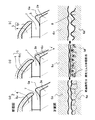
前述したように、TMAH等のアルカリ液中における第一の導電材料層6aのエッチング処理では、第一の導電材料層6aの膜密度が高いほどエッチングレートが遅い。工程4で形成した1.0Pa以下の圧力下でスパッタされた第一の導電材料層6aに対しては、例えば高濃度のTMAH水溶液を用いることで、第一の導電材料層6aに有意な頂部8を形成することができる。図10にMoの第一の導電材料層6aをエッチングした時の変化を示す。エッチング液に浸漬した初期の段階ではMoの酸化が進行する。まず、MoはMoOxに酸化され、膜の体積膨張が起きる。更に酸化が進行し、MoOxはMoO42-として液中へ溶解する。図10(a)はエッチング前の凹部7周りの断面図と正面図である。図10(b)は、エッチングの初期段階の凹部7周りの断面図と正面図で、Moの第一の導電材料層6aの表面が酸化により体積膨張し、MoとMo酸化物が混在した表面となった状態を示す。また、図10(b)に示されるように、同じMo膜であっても、その中で電位が卑な部位と貴な部位がそれぞれ存在した状態となっている。エッチングの完了時の凹部7周りの断面図と正面図である図10(c)に示すように、エッチングの進行と共に卑な部位のMoはイオン化して溶解し、貴な部位はそのまま残る。つまり第一の導電材料層6aの突起部では、図10(b)に示されるように、溶解した部位と残された部分とが生じ、残された部位が複数の頂部8を形成する。 As described above, in the etching process of the first conductive material layer 6a in an alkaline solution such as TMAH, the higher the film density of the first conductive material layer 6a, the slower the etching rate. For the first conductive material layer 6a sputtered under a pressure of 1.0 Pa or less formed in step 4, for example, by using a high-concentration TMAH aqueous solution, a significant top portion of the first conductive material layer 6a is obtained. 8 can be formed. FIG. 10 shows a change when the first conductive material layer 6a of Mo is etched. At the initial stage of immersion in the etching solution, Mo oxidation proceeds. First, Mo is oxidized to MoOx, and the volume expansion of the film occurs. Further, the oxidation proceeds, and MoOx is dissolved into the liquid as MoO4 2− . FIG. 10A is a cross-sectional view and a front view around the recess 7 before etching. FIG. 10B is a cross-sectional view and a front view of the periphery of the recess 7 in the initial stage of etching, and the surface of the Mo first conductive material layer 6a is volume-expanded by oxidation, and the surface is a mixture of Mo and Mo oxide. This shows the state. Further, as shown in FIG. 10B, even in the same Mo film, there are a portion having a low potential and a noble portion in the same Mo film. As shown in FIG. 10C, which is a cross-sectional view and a front view of the periphery of the recess 7 when etching is completed, the base portion of Mo is ionized and dissolved with the progress of etching, and the precious portion remains as it is. That is, as shown in FIG. 10B, a melted portion and a remaining portion are generated in the protruding portion of the first conductive material layer 6 a, and the remaining portions form a plurality of top portions 8.

頂部8は、先行文献に示されるように、第一の導電材料層6aのスパッタリング法による成膜時にスパッタ圧力の制御で高さを調整しながら形成することもできる。しかし、上記のようにして頂部8を形成すると、高さの揃った頂部8を多数形成しやすいことから好ましい。   As shown in the prior art, the top portion 8 can also be formed while adjusting the height by controlling the sputtering pressure when the first conductive material layer 6a is formed by sputtering. However, it is preferable to form the top portion 8 as described above because a large number of top portions 8 having the same height can be easily formed.

(工程6の詳細)
工程6は、概要を図5(a)で説明した第二の導電材料層6bを設ける工程である。第二の導電材料層6bは、副頂部9〔図5(b)参照〕を構成するもので、全圧が1.0Pa以上2.8Pa以下の圧力範囲で、第一の導電材料層6aの上にスパッタリング法により堆積する。このようにして図5(a)に示すように第二の導電材料層6bが形成され、詳しくは後述するが、エッチングにより、副頂部9が形成される。第二の導電材料層6bの膜厚は5nmから50nmの範囲で設定され、好ましくは10nmから25nmの範囲で選択される。また、図5(a)に示すように、第二の導電材料層6bは、カソード6上及びゲート5上に形成され、本例においては、カソード6上の第二の導電材料層6bと、ゲート5上の第二の導電材料層6bとは接凹部7付近で接点を有するものとなっている。
(Details of step 6)
Step 6 is a step of providing the second conductive material layer 6b whose outline has been described with reference to FIG. The second conductive material layer 6b constitutes the sub-top 9 (see FIG. 5B), and the total pressure of the first conductive material layer 6a is within a pressure range of 1.0 Pa to 2.8 Pa. Deposited by sputtering. In this way, the second conductive material layer 6b is formed as shown in FIG. 5A. As will be described in detail later, the sub-top portion 9 is formed by etching. The film thickness of the second conductive material layer 6b is set in the range of 5 nm to 50 nm, and preferably selected in the range of 10 nm to 25 nm. Also, as shown in FIG. 5A, the second conductive material layer 6b is formed on the cathode 6 and the gate 5, and in this example, the second conductive material layer 6b on the cathode 6; The second conductive material layer 6 b on the gate 5 has a contact in the vicinity of the contact recess 7.

前述したように、全圧が1.0Pa以上2.8Pa以下の圧力範囲でスパッタリング法により堆積された導電性膜は、結晶粒界部分が多く、膜密度は低い。エッチングレートは、全圧1.0Pa以下のスパッタリングで形成した導電性膜よりも著しく速く、同一条件のエッチングで30〜40倍速い。これは、これは次工程の第四のエッチング処理で第二の導電材料層6bをエッチングしたときに、先に説明した第一の導電性材料層6aであるカソード6を残すことができるエッチングレート比である。なお、図5(a)では、カソード6上の第二の導電材料層6bと、ゲート5上の第二の導電材料層6bとが接触するように成膜した例を示している。しかし、カソード6上の第二の導電材料層6bと、ゲート5上の第二の導電材料層6bとが接触しないように成膜する場合もある。また、第二の導電材料層6bをカソード6の先端部に形成された頂部8の内側斜面をも含む領域に堆積させるためには、工程4と同様に、指向性スパッタリング法を用いることが好ましい。   As described above, the conductive film deposited by the sputtering method in the pressure range of 1.0 Pa or more and 2.8 Pa or less has many crystal grain boundary portions and the film density is low. The etching rate is significantly faster than the conductive film formed by sputtering with a total pressure of 1.0 Pa or less, and is 30 to 40 times faster when etching under the same conditions. This is an etching rate that can leave the cathode 6 that is the first conductive material layer 6a described above when the second conductive material layer 6b is etched in the fourth etching process of the next step. Is the ratio. FIG. 5A shows an example in which the second conductive material layer 6b on the cathode 6 and the second conductive material layer 6b on the gate 5 are in contact with each other. However, the second conductive material layer 6b on the cathode 6 and the second conductive material layer 6b on the gate 5 may be formed so as not to contact each other. Further, in order to deposit the second conductive material layer 6 b in a region including the inner slope of the top 8 formed at the tip of the cathode 6, it is preferable to use a directional sputtering method as in Step 4. .

(工程7の詳細)
工程7は、概要を図5(b)で説明した第四のエッチング処理を行う工程である。本工程では、第二の導電材料層6bに対して第四のエッチング処理を行い、副頂部9を形成する。図11(a)はエッチング初期の凹部7周りの断面図と正面図、図11(b)エッチング中期の凹部7周りの断面図と正面図、図11(c)はエッチング完了時の凹部7周りの断面図と正面図である。図11(a)から(b)の変化として示すように、カソード6上の第二の導電材料層6bと、ゲート5上の第二の導電材料層6bとの接触点の部分は、エッチングの過程でエッチングされにくい部分としてブリッジを生じる。更にエッチングが進行すると、ブリッジを形成していた第二の導電材料層6bは溶解し始める。そして、頂部8の内側斜面の第二の導電材料層6bはエッチング処理で溶解しにくく、その結果として図11(c)に示すように副頂部9として残すことができる。
(Details of step 7)
Step 7 is a step of performing the fourth etching process whose outline has been described with reference to FIG. In this step, a fourth etching process is performed on the second conductive material layer 6 b to form the sub-top portion 9. 11A is a cross-sectional view and a front view around the recess 7 in the initial stage of etching, FIG. 11B is a cross-sectional view and a front view around the recess 7 in the middle of etching, and FIG. It is sectional drawing and front view. As shown in FIG. 11 (a) to FIG. 11 (b), the portion of the contact point between the second conductive material layer 6b on the cathode 6 and the second conductive material layer 6b on the gate 5 is etched. In the process, a bridge is formed as a portion that is difficult to be etched. As the etching further proceeds, the second conductive material layer 6b forming the bridge starts to dissolve. The second conductive material layer 6b on the inner slope of the top 8 is hardly dissolved by the etching process, and as a result, can be left as a sub-top 9 as shown in FIG.

上述したブリッジを経て形成される副頂部9は、ゲート5とカソード6間の間隔が狭くなっている箇所のカソード6の表面に位置する。また、副頂部9は、頂部8の内側斜面から斜め凹部7の内側向きに形成される。副頂部9が突出する方向は、頂部8の内側斜面からゲート5への最短方向となる。副頂部9の位置は、工程2で第一の絶縁層3aの側面部の傾斜角θが50〜60度と小さくなるようにエッチングしておくと、ゲート5が凹部7の下縁より後退するために、頂部8の内側斜面の下方寄りとなり、結果として頂部8から離れる。第一の絶縁層3aの側面部の傾斜角θが90度に近いと、頂部8の内側斜面の上方寄りとなり、結果として頂部8に近付く。頂部8と頂部9がある程度離れていた方が両者を共に電子得放出点として機能させやすいので、第一の絶縁層3aの側面部の傾斜角θは50〜60度であることが好ましい。また、後退したゲート5が得やすいことから、ゲート5を構成する導電材料層4の側面部の傾斜角は第一の絶縁層3aの側面部の傾斜角より小さいことが好ましい。   The sub-top portion 9 formed through the bridge described above is located on the surface of the cathode 6 where the distance between the gate 5 and the cathode 6 is narrow. The sub-top portion 9 is formed from the inner slope of the top portion 8 toward the inner side of the oblique recess portion 7. The direction in which the sub-top portion 9 protrudes is the shortest direction from the inner slope of the top portion 8 to the gate 5. If the sub-top portion 9 is etched in step 2 so that the inclination angle θ of the side surface portion of the first insulating layer 3a is as small as 50 to 60 degrees, the gate 5 recedes from the lower edge of the concave portion 7. For this reason, it becomes closer to the lower side of the inner slope of the top 8, and as a result, moves away from the top 8. When the inclination angle θ of the side surface portion of the first insulating layer 3a is close to 90 degrees, the first insulating layer 3a approaches the top portion 8 as a result of being closer to the upper side of the inner slope of the top portion 8. Since it is easier for both the top portion 8 and the top portion 9 to function as electron emission and emission points when the top portion 8 and the top portion 9 are separated from each other, the inclination angle θ of the side surface portion of the first insulating layer 3a is preferably 50 to 60 degrees. In addition, since the receded gate 5 is easily obtained, the inclination angle of the side surface portion of the conductive material layer 4 constituting the gate 5 is preferably smaller than the inclination angle of the side surface portion of the first insulating layer 3a.

図11では、カソード6上の第二の導電材料層6bと、ゲート5上の第二の導電材料層6bとが接触するようにスパッタリングされた状態からのエッチング処理の態様を示している。しかし、カソード6上の第二の導電材料層6bと、ゲート5上の第二の導電材料層6bとが接触しないように成膜されている場合でも、エッチング液に浸漬された初期の段階で両者が酸化されて体積膨張を起こすことで接点が生じるようにすることもできる。   FIG. 11 shows an aspect of the etching process from a state in which the second conductive material layer 6b on the cathode 6 and the second conductive material layer 6b on the gate 5 are sputtered so as to be in contact with each other. However, even when the second conductive material layer 6b on the cathode 6 and the second conductive material layer 6b on the gate 5 are formed so as not to come into contact with each other, at the initial stage of being immersed in the etching solution. It is also possible to generate a contact point by causing volume expansion by oxidizing both.

次に、上記製造方法により形成される電子放出素子の頂部9とその周辺構造について説明する。   Next, the top part 9 of the electron-emitting device formed by the above manufacturing method and its peripheral structure will be described.

図2に示すように、カソード6は、凹部7の下縁の長さ方向に沿って並んで設けられた複数の頂部8を備えている。副頂部9はこの頂部8の内側斜面とゲート5の最短間隔部に形成される。そして、副頂部9のような微小突起が、頂部8と共に凹部7の下縁の長さ方向に複数並んでいることになる。頂部8は凹部7の下縁から上方へ突起しており、後述するアノード18(図12参照)に向かって突出した形態となる。一方、副頂部9は、上述したカソード6の頂部8の内側斜面に形成され、頂部10の突出する方向はゲート5との最短方向へ向かっているのが特徴である。   As shown in FIG. 2, the cathode 6 includes a plurality of top portions 8 provided side by side along the length direction of the lower edge of the recess 7. The sub-top 9 is formed at the shortest distance between the inner slope of the top 8 and the gate 5. Then, a plurality of minute projections such as the sub-top portion 9 are arranged in the length direction of the lower edge of the concave portion 7 together with the top portion 8. The top 8 protrudes upward from the lower edge of the recess 7 and protrudes toward an anode 18 (see FIG. 12) described later. On the other hand, the sub-top portion 9 is formed on the inner slope of the top portion 8 of the cathode 6 described above, and the projecting direction of the top portion 10 is directed to the shortest direction with the gate 5.

なお、図2ではゲート5を構成する導電材料層4の側面部から第一の導電材料層6aが垂れ下がった態様で図示しているが、第一の導電材料層6aの膜厚が薄い場合は、導電材料層4がカソード6との狭部を形成することもある。この場合、副頂部9は、頂部8の内側斜面と導電材料層4との間で生じる狭部のうち、最も近接した部位に形成され、副頂部9の突出する方向は導電材料層4との最短部に向かう方向ということになる。   In FIG. 2, the first conductive material layer 6 a is illustrated as hanging from the side surface portion of the conductive material layer 4 constituting the gate 5. However, when the first conductive material layer 6 a is thin, The conductive material layer 4 may form a narrow portion with the cathode 6. In this case, the sub-top portion 9 is formed in the closest portion among the narrow portions generated between the inner slope of the top portion 8 and the conductive material layer 4, and the direction in which the sub-top portion 9 protrudes from the conductive material layer 4. That is the direction toward the shortest part.

頂部8の内側斜面に突出して、副頂部9は設けられている。副頂部9の周囲とゲート5との距離は、副頂部9とゲート5との距離よりも広くなる。副頂部9から放出された電子はゲート5で等方的に散乱するが、散乱した電子のうち、副頂部9の両脇に散乱した電子は、ゲート5との間隔が広い部分を抜けてアノード18(図12参照)に到達することができる。これも放出特性を向上させる原因の一つである。   A sub-top portion 9 is provided so as to protrude from the inner slope of the top portion 8. The distance between the periphery of the sub-top portion 9 and the gate 5 is larger than the distance between the sub-top portion 9 and the gate 5. Electrons emitted from the sub-top portion 9 are isotropically scattered at the gate 5, but among the scattered electrons, electrons scattered on both sides of the sub-top portion 9 pass through a portion having a wide interval with the gate 5 and become the anode. 18 (see FIG. 12). This is one of the reasons for improving the release characteristics.

図2に示されるように、副頂部9を拡大すると、その先端部は曲率半径rで代表される形状を有する。この曲率半径rに依存して、先端部の電界強度が変化する。rが小さいほど電気力線の集中が生じるため、副頂部9の先端に高い電界を形成することが可能となる。実用的にはrは2nm以上12nm以下でより好ましくは2nm以上5nm以下である。ゲート5と副頂部9との間隔d′は、ゲート5での電子の散乱回数の違いに影響するため、d′が大きいほど電子放出効率を高くすることができる。また、放出電流量を向上させることができる。電子を放出させるのに必要な駆動電圧は、d′が10nmより大きいと大きくなりすぎる。また、駆動時の安定性の観点から、d′が1nm以上となることが好ましい。1nmより小さいと、電界蒸発や放電、短絡等により副頂部9が駆動時に破壊される可能性がある。そのため、実用的にはd′は1nm以上10nm以下で、より好ましくは4nm以上8nm以下である。また、副頂部9の高さは、2nm以上10nm以下であることが好ましい。   As shown in FIG. 2, when the sub-top portion 9 is enlarged, the tip portion has a shape represented by a curvature radius r. Depending on the radius of curvature r, the electric field strength at the tip changes. As r is smaller, the lines of electric force are concentrated, so that a high electric field can be formed at the tip of the sub-top portion 9. Practically, r is 2 nm or more and 12 nm or less, more preferably 2 nm or more and 5 nm or less. Since the distance d ′ between the gate 5 and the sub-top portion 9 affects the difference in the number of electron scattering at the gate 5, the larger the d ′, the higher the electron emission efficiency. In addition, the amount of emission current can be improved. The drive voltage required to emit electrons becomes too large when d 'is greater than 10 nm. In addition, d ′ is preferably 1 nm or more from the viewpoint of stability during driving. If it is smaller than 1 nm, the sub-top portion 9 may be destroyed during driving due to field evaporation, discharge, short circuit, or the like. Therefore, practically, d ′ is 1 nm or more and 10 nm or less, more preferably 4 nm or more and 8 nm or less. Moreover, it is preferable that the height of the sub-top part 9 is 2 nm or more and 10 nm or less.

従来の電子放出素子では、頂部8をカソードに形成し、この頂部8を電子放出点として機能させていたが、更に副頂部9を、前述した製造方法により、頂部8の内側斜面に形成したことにより、電子放出点を増やすことができる。また、ゲート5とカソード6の頂部8間の最短部に副頂部9を形成することが可能で、これにより、副頂部9の先端とゲート5との距離を、好ましい範囲である1nm以上10nm以下に制御することが容易となる。その結果、電子放出効率が高く、放出電流量がより向上する電子放出素子を形成することができる。また、そのような電子放出素子を大面積に形成することが可能となる。   In the conventional electron-emitting device, the top 8 is formed on the cathode, and this top 8 functions as an electron emission point, but the sub-top 9 is further formed on the inner slope of the top 8 by the manufacturing method described above. As a result, the number of electron emission points can be increased. Further, it is possible to form the sub-top portion 9 at the shortest portion between the gate 5 and the top portion 8 of the cathode 6, whereby the distance between the tip of the sub-top portion 9 and the gate 5 is a preferable range of 1 nm to 10 nm. It becomes easy to control. As a result, it is possible to form an electron-emitting device with high electron emission efficiency and a further improved emission current amount. In addition, such an electron-emitting device can be formed in a large area.

次に、本発明の製造方法によって製造された電子放出素子を用いた電子線装置の一例を図12で説明する。この電子線装置は、電子放出素子の電子放出特性の測定装置として用いることもできる。この電子線装置は、本発明の製造方法によって製造された電子放出素子のカソード6を、駆動のための配線2に接続し、前記頂部8及び副頂部に対向させて、ゲート5を介してアノード18を配置することで得ることができる。この装置において、カソード6から放出された電子のアノード18への到達効率である電子放出効率(η)は、電子放出素子の駆動時に検出される素子電流Ifと、真空中を介してアノード18へ到達する電流である放出電流Ieを用いて求められる。即ち、η=Ie/(If+Ie)で与えられる。電子放出特性の測定は図12に示す構成で行うことができる。図12において、Vfはゲート5とカソード6の間に印加する電圧であり、IfはVfをゲート5とカソード6の間に印加した際にゲート5とカソード6の間に流れる素子電流である。また、Vaはカソード6とアノード18の間に印加される電圧であり、Ieは放出電流である。なお、ここでは、Vaをカソード6とアノード18の間に印加する例を示したが、アノード18に電位を印加する電源と、カソード6に電位を印加する電源とを別々に設けても良い。図12に示すように、電子放出素子が設けられた基板1の上方に、ゲート5およびカソード6よりも高電位に規定されるアノード18を設けることで、複数の頂部8及び副頂部9から放出された電子をアノード18に到達させる電子線装置が構成される。   Next, an example of an electron beam apparatus using the electron-emitting device manufactured by the manufacturing method of the present invention will be described with reference to FIG. This electron beam apparatus can also be used as a measuring apparatus for electron emission characteristics of an electron-emitting device. In this electron beam apparatus, the cathode 6 of the electron-emitting device manufactured by the manufacturing method of the present invention is connected to the wiring 2 for driving, and is opposed to the top 8 and the sub-top, and the anode is connected through the gate 5. It can be obtained by arranging 18. In this device, the electron emission efficiency (η), which is the arrival efficiency of electrons emitted from the cathode 6 to the anode 18, is the device current If detected when the electron-emitting device is driven and the anode 18 through the vacuum. It is obtained using the emission current Ie which is the current that reaches. That is, η = Ie / (If + Ie). The electron emission characteristics can be measured with the configuration shown in FIG. In FIG. 12, Vf is a voltage applied between the gate 5 and the cathode 6, and If is an element current flowing between the gate 5 and the cathode 6 when Vf is applied between the gate 5 and the cathode 6. Va is a voltage applied between the cathode 6 and the anode 18, and Ie is an emission current. Although an example in which Va is applied between the cathode 6 and the anode 18 is shown here, a power source that applies a potential to the anode 18 and a power source that applies a potential to the cathode 6 may be provided separately. As shown in FIG. 12, an anode 18 defined at a higher potential than the gate 5 and the cathode 6 is provided above the substrate 1 on which the electron-emitting devices are provided, thereby emitting light from the plurality of top portions 8 and sub-top portions 9. An electron beam apparatus is configured to cause the electrons to reach the anode 18.

次に、上記のような電子線装置を用いた画像表示装置について、図13を用いて説明する。   Next, an image display apparatus using the above electron beam apparatus will be described with reference to FIG.

図13(a)は電子放出素子をマトリクス状に配置した電子源を用いて構成したディスプレイパネル77の一例を示す模式図であり、内部がわかるように一部を切り欠いて示している。図13(a)において、61は電子源基板、62はX方向配線、63はY方向配線であり、電子源基板61は先に説明した電子放出素子の基板1に相当する。また、64は上記した電子放出素子群を模式的に示している。なお、X方向配線62は、上述のカソード6を共通に接続する配線であり、Y方向配線63は上述のゲート5を共通に接続する配線である。ここでは、電子放出素子が、X方向配線62とY方向配線63の交差部に設けた例を模式的に示しているが、電子放出素子は、X方向配線62とY方向配線63の交差部の脇の電子源基板61上に設けることができる。   FIG. 13A is a schematic view showing an example of a display panel 77 configured using an electron source in which electron-emitting devices are arranged in a matrix, and a part thereof is cut away so that the inside can be seen. In FIG. 13A, 61 is an electron source substrate, 62 is an X direction wiring, and 63 is a Y direction wiring. The electron source substrate 61 corresponds to the substrate 1 of the electron-emitting device described above. Reference numeral 64 schematically represents the above-described electron-emitting device group. The X-direction wiring 62 is a wiring that commonly connects the cathodes 6 described above, and the Y-direction wiring 63 is a wiring that commonly connects the gates 5 described above. Here, an example in which the electron-emitting device is provided at the intersection of the X-direction wiring 62 and the Y-direction wiring 63 is shown schematically, but the electron-emitting device is an intersection of the X-direction wiring 62 and the Y-direction wiring 63. Can be provided on the electron source substrate 61 on the side.

X方向配線62には、X方向に配列した電子放出素子64の行を選択するための走査信号を印加する、不図示の走査信号印加手段が接続される。一方、Y方向配線63には、Y方向に配列した電子放出素子64の各列を入力信号に応じて変調するための、不図示の変調信号発生手段が接続される。各電子放出素子に印加される駆動電圧は、当該素子に印加される走査信号と変調信号の差電圧として供給される。この構成においては、単純なマトリクス配線を用いて、個別の電子放出素子64を選択して、独立に駆動可能とすることができる。   The X-direction wiring 62 is connected to a scanning signal applying unit (not shown) that applies a scanning signal for selecting a row of the electron-emitting devices 64 arranged in the X direction. On the other hand, the Y direction wiring 63 is connected to a modulation signal generating means (not shown) for modulating each column of the electron-emitting devices 64 arranged in the Y direction according to an input signal. The drive voltage applied to each electron-emitting device is supplied as a difference voltage between the scanning signal and the modulation signal applied to the device. In this configuration, individual electron-emitting devices 64 can be selected and driven independently using simple matrix wiring.

図13(a)において、電子源基板61はリアプレート71に固定されている。また、ガラス基板73の内面に、電子放出素子から放出された電子が照射されることで発光する例えば蛍光体からなる発光体74と、前述したアノード18に相当するメタルバック75と、を積層してフェースプレート76を構成している。また、リアプレート71とフェースプレート76が、リアプレート71とフェースプレート76との間に設けられた支持枠72と、フリットガラス等の接合部材を介して、気密に接合されて、ディスプレィパネル77が構成されている。ディスプレィパネル77は、上述の如く、フェースプレート76、支持枠72、リアプレート71で構成される。ここで、リアプレート71は主に電子源基板61の強度を補強する目的で設けられるため、電子源基板61自体で十分な強度を持つ場合には、別体のリアプレート71は不要とすることができる。一方、フェースプレート76とリアプレート71との間に、スペーサーとよばれる不図示の支持体を設置することにより、大気圧に対して十分な強度を持たせた構成とすることもできる。   In FIG. 13A, the electron source substrate 61 is fixed to the rear plate 71. Further, on the inner surface of the glass substrate 73, a light emitting body 74 made of, for example, a phosphor that emits light when irradiated with electrons emitted from the electron emitting element, and a metal back 75 corresponding to the anode 18 described above are laminated. The face plate 76 is configured. Further, the rear plate 71 and the face plate 76 are hermetically joined via a support frame 72 provided between the rear plate 71 and the face plate 76 and a joining member such as frit glass, and the display panel 77 is thereby joined. It is configured. The display panel 77 includes the face plate 76, the support frame 72, and the rear plate 71 as described above. Here, since the rear plate 71 is provided mainly for the purpose of reinforcing the strength of the electron source substrate 61, if the electron source substrate 61 itself has sufficient strength, the separate rear plate 71 is not required. Can do. On the other hand, by providing a support (not shown) called a spacer between the face plate 76 and the rear plate 71, it is possible to provide a structure with sufficient strength against atmospheric pressure.

次に、図13b)のブロック図を用いて、上述したディスプレィパネル77を備えた画像表示装置25並びにテレビジョン装置27について説明する。   Next, the image display device 25 and the television device 27 including the display panel 77 will be described with reference to the block diagram of FIG.

受信回路20は、チューナーやデコーダ等からなり、衛星放送や地上波等のテレビ信号、ネットワークを介したデータ放送等の各種の信号を受信し、復号化した映像データを画像処理部21に出力する。尚、上記した「受信した信号」は「入力された信号」と言い換えることができる。画像処理部21はγ補正回路や解像度変換回路やI/F回路等を含み、画像処理された映像データをディスプレイ(画像表示装置)25の表示フォーマットに変換して画像表示装置25に画像信号として出力する。   The receiving circuit 20 includes a tuner, a decoder, and the like, receives various signals such as satellite broadcasting and terrestrial television signals, and data broadcasting via a network, and outputs decoded video data to the image processing unit 21. . The above-mentioned “received signal” can be rephrased as “input signal”. The image processing unit 21 includes a γ correction circuit, a resolution conversion circuit, an I / F circuit, and the like. The image processing unit 21 converts the image-processed video data into a display format of a display (image display device) 25 and sends it to the image display device 25 as an image signal. Output.

画像表示装置25は、前述したディスプレィパネル77を少なくとも含み、さらに、駆動回路及び駆動回路を制御する制御回路22をも含む。制御回路22は、入力した画像信号に補正処理等の信号処理を施すとともに、駆動回路に画像信号及び各種制御信号を出力する。制御回路22には、同期信号分離回路、RGB変換回路、輝度信号変換部、タイミング制御回路等が含まれる。駆動回路は、入力された画像信号に基づいて、ディスプレィパネル77内部の電子放出素子に駆動信号を出力し、駆動信号に基づきテレビ映像が表示される。駆動回路には、走査回路や変調回路やアノード電位を供給する高圧電源回路等が含まれる。受信回路20と画像処理回路21は、セットトップボックス(STB26)として画像表示装置25とは別の筐体に収められていてもよいし、また、画像表示装置25と一体の筐体に収められていてもよい。ここでは、テレビジョン装置27がテレビ映像を表示する例を説明した。しかし、受信回路20をインターネット等の回線を通じて配信される映像を受信する回路とすれば、テレビジョン装置27は、テレビ映像に限らず、様々な映像を表示することができる映像表示装置として機能する。   The image display device 25 includes at least the display panel 77 described above, and further includes a drive circuit and a control circuit 22 that controls the drive circuit. The control circuit 22 performs signal processing such as correction processing on the input image signal, and outputs the image signal and various control signals to the drive circuit. The control circuit 22 includes a synchronization signal separation circuit, an RGB conversion circuit, a luminance signal conversion unit, a timing control circuit, and the like. The drive circuit outputs a drive signal to the electron-emitting devices inside the display panel 77 based on the input image signal, and a television image is displayed based on the drive signal. The drive circuit includes a scanning circuit, a modulation circuit, a high-voltage power supply circuit that supplies an anode potential, and the like. The receiving circuit 20 and the image processing circuit 21 may be housed in a housing separate from the image display device 25 as a set-top box (STB 26), or in a housing integral with the image display device 25. It may be. Here, an example in which the television device 27 displays a television image has been described. However, if the receiving circuit 20 is a circuit that receives video distributed through a line such as the Internet, the television device 27 functions as a video display device capable of displaying various videos as well as television videos. .

なお、本発明で製造した電子放出素子を用いた電子線装置は、上記のような画像表示装置25だけではなく、アノード49として電子の照射によってX線を発生するターゲットを用いることで、X線装置を構成することもできる。   The electron beam apparatus using the electron-emitting device manufactured according to the present invention uses not only the image display device 25 as described above but also a target that generates X-rays by electron irradiation as the anode 49, so that X-rays can be obtained. An apparatus can also be constructed.

以下、上記実施の形態に基づいたより具体的な実施例について説明する。   Hereinafter, more specific examples based on the above embodiment will be described.

(実施例1)
図3〜図5を参照しながら、本実施例の電子放出素子の製造方法を説明する。
Example 1
A method for manufacturing the electron-emitting device of this example will be described with reference to FIGS.

最初に図3(a)に示すように基板1上に、第一の絶縁材料層3aと、第二の絶縁材料層3bと、導電材料層4とを順次積層する。基板1としては高歪点低ナトリウムガラス(旭硝子株式会社製 PD200)を用いた。第一の絶縁材料層3aは、窒化シリコン膜をスパッタリング法にて形成し、その厚さとしては500nmとした。第二の絶縁材料層3bは、酸化シリコン膜をスパッタリング法にて形成し、その厚さとしては30nmとした。導電材料層4は窒化タンタル膜をスパッタリング法にて形成し、その厚さとしては30nmとした。   First, as shown in FIG. 3A, a first insulating material layer 3a, a second insulating material layer 3b, and a conductive material layer 4 are sequentially laminated on the substrate 1. As the substrate 1, high strain point low sodium glass (PD200 manufactured by Asahi Glass Co., Ltd.) was used. As the first insulating material layer 3a, a silicon nitride film was formed by a sputtering method, and the thickness thereof was set to 500 nm. As the second insulating material layer 3b, a silicon oxide film was formed by a sputtering method, and the thickness thereof was 30 nm. As the conductive material layer 4, a tantalum nitride film was formed by a sputtering method, and its thickness was 30 nm.

次に、図3(b)に示すように、フォトリソグラフィー技術により導電材料層4上にレジストパターンを形成した後、ドライエッチング法を用いて、導電材料層4、第二の絶縁材料層3b、第一の絶縁材料層3aを順に加工した。この第一のエッチング処理により、上面に導電材料層4が設けられ、基板1の表面から立ち上がった側面部を有する絶縁部材3を形成した。この時のエッチングガスとしては、第一及び第二の絶縁材料層3a,3b及び導電材料層4にはフッ化物を作る材料が選択されているため、CF4系のガスを用いた。このガスを用いてRIEを行った結果、エッチング後の傾斜角は、第一の絶縁材料層3aの側面部で50度〜60度、導電材料層4の側面部でおよそ40度であった。 Next, as shown in FIG. 3B, after a resist pattern is formed on the conductive material layer 4 by a photolithography technique, the conductive material layer 4, the second insulating material layer 3b, The first insulating material layer 3a was processed in order. By this first etching process, the conductive material layer 4 was provided on the upper surface, and the insulating member 3 having a side surface rising from the surface of the substrate 1 was formed. As the etching gas at this time, a CF 4 -based gas was used because the first and second insulating material layers 3a and 3b and the conductive material layer 4 are made of a material that produces fluoride. As a result of performing RIE using this gas, the inclination angle after etching was 50 to 60 degrees at the side surface portion of the first insulating material layer 3a and about 40 degrees at the side surface portion of the conductive material layer 4.

レジストを剥離した後、図3(c)に示すようにBHF(ステラケミファ(株)製 高純度バッファードフッ酸LAL100)を用いて、凹部7の深さが約70nmになるように第二の絶縁材料層3bをエッチングした。BHFは、NH4HF2=0.9wt%とNF4F=16.4wt%の混合物である。この第二のエッチング処理により、絶縁部材3の側面部の導電材料層4の直下に凹部7を形成した。 After removing the resist, as shown in FIG. 3 (c), using BHF (Stella Chemifa Co., Ltd., high-purity buffered hydrofluoric acid LAL100), the depth of the recess 7 is about 70 nm. The insulating material layer 3b was etched. BHF is a mixture of NH 4 HF 2 = 0.9 wt% and NF 4 F = 16.4 wt%. By this second etching process, a recess 7 was formed immediately below the conductive material layer 4 on the side surface of the insulating member 3.

次に、図4(a)に示すように、第一の絶縁材料層3aの側面部上及び凹部7中に露出した上面部上、更には導電材料層4上に、少なくとも第一の絶縁材料層3aの側面部上の厚さが25nmになるようにモリブデン(Mo)を指向性スパッタリング法で堆積させた。スパッタリングは、基板1の表面がスパッタタ−ゲットに対して水平になるようにセットして行った。本実施例では、スパッタ粒子が限られた角度(具体的には基板1の表面に対して90±10°)で基板1の表面に入射されるよう、基板1とターゲットの間に遮蔽板を設けた。また、スパッタリング時のアルゴンプラズマのパワーを1W/cm2、基板1とターゲットとの間の距離を100mm、全圧を0.4Paとした。そして、凹部7内への第一の導電材料層6aの構成材料の入り込み量〔図2(c)における距離X〕が35nmとなるように第一の導電材料層6aを形成した。本実施例では、第一の絶縁材料層3aの側面部上と導電材料層4上とに同時に成膜した。更に、フォトリソグラフィー技術とMoのドライエッチング法を用いて、第一の導電材料層6aのパターン形成を行った。 Next, as shown in FIG. 4A, at least a first insulating material is formed on the side surface of the first insulating material layer 3a, the upper surface exposed in the recess 7, and further on the conductive material layer 4. Molybdenum (Mo) was deposited by directional sputtering so that the thickness on the side surface of the layer 3a was 25 nm. Sputtering was performed by setting the surface of the substrate 1 so as to be horizontal with respect to the sputtering target. In this embodiment, a shielding plate is provided between the substrate 1 and the target so that the sputtered particles are incident on the surface of the substrate 1 at a limited angle (specifically, 90 ± 10 ° with respect to the surface of the substrate 1). Provided. The power of argon plasma during sputtering was 1 W / cm 2 , the distance between the substrate 1 and the target was 100 mm, and the total pressure was 0.4 Pa. Then, the first conductive material layer 6a was formed such that the amount of the constituent material of the first conductive material layer 6a into the recess 7 [distance X in FIG. 2 (c)] was 35 nm. In this example, the film was formed simultaneously on the side surface portion of the first insulating material layer 3 a and the conductive material layer 4. Further, the pattern of the first conductive material layer 6a was formed by using the photolithography technique and the Mo dry etching method.

次に、図4(b)に示すように、第一の導電材料層6aに対するウェットエッチング処理(第三のエッチング処理)を行った。エッチング液には濃度2.38wt%のTMAH(テトラメチルアンモニウムハイドライド)水溶液を用いた。このエッチング液に第一の導電材料層6aを180秒間浸漬処理した後に、流水で5分間洗浄した。このようにして第一の導電材料層6aに対するアルカリ処理を行うことで、第一の導電材料層6aの突起部に、凹部7の下縁の長さ方向に沿って多数の頂部8を形成した。   Next, as shown in FIG. 4B, a wet etching process (third etching process) was performed on the first conductive material layer 6a. As the etching solution, a 2.38 wt% TMAH (tetramethylammonium hydride) aqueous solution was used. The first conductive material layer 6a was immersed in this etching solution for 180 seconds, and then washed with running water for 5 minutes. By performing the alkali treatment on the first conductive material layer 6a in this way, a large number of top portions 8 are formed along the length direction of the lower edge of the concave portion 7 at the protrusions of the first conductive material layer 6a. .

次に、図5(a)に示すように、第一の導電材料層6aの上に、第二の導電材料層6bとして、膜厚が20nmなるようにモリブデン(Mo)を指向性スパッタリング法により堆積させた。スパッタリングは1.7Paの全圧下で行った。第二の導電材料層6bの成膜は、カソード6側の第二の導電材料層6bとゲート5側の第二の導電材料層6bとの間に接点を生じるように行った。更に、フォトリソグラフィー技術とMoのドライエッチング法を用いて、第二の導電材料層6bのパターン形成を行った。   Next, as shown in FIG. 5A, molybdenum (Mo) is deposited on the first conductive material layer 6a as a second conductive material layer 6b by a directional sputtering method so as to have a film thickness of 20 nm. Deposited. Sputtering was performed under a total pressure of 1.7 Pa. The second conductive material layer 6b was formed so that a contact was formed between the second conductive material layer 6b on the cathode 6 side and the second conductive material layer 6b on the gate 5 side. Further, the pattern of the second conductive material layer 6b was formed by using the photolithography technique and the Mo dry etching method.

最後に、図5(b)に示すように、第二の導電材料層6bに対するウェットエッチング処理(第四のエッチング処理)を行った。エッチング液には濃度0.3wt%のTMAH(テトラメチルアンモニウムハイドライド)水溶液を用いた。このエッチング液に第二の導電材料層6bを60秒間浸漬処理した後に、流水で5分間洗浄した。このようにして第二の導電材料膜6bに対するアルカリ処理を行うことで、第一の導電材料層6aの突起部に形成された頂部8の内側斜面に残留した第二の導電材料層6bで副頂部9を形成した。   Finally, as shown in FIG. 5B, a wet etching process (fourth etching process) was performed on the second conductive material layer 6b. As the etching solution, a TMAH (tetramethylammonium hydride) aqueous solution having a concentration of 0.3 wt% was used. The second conductive material layer 6b was immersed in this etching solution for 60 seconds, and then washed with running water for 5 minutes. By performing the alkali treatment on the second conductive material film 6b in this way, the second conductive material layer 6b remaining on the inner slope of the top portion 8 formed on the protrusion of the first conductive material layer 6a is sub-charged. A top 9 was formed.

上記の工程で得た電子放出素子をマトリクス状に配列して電子源を作製し、これを用いて、図13(a)に示すディスプレィパネル77を作製した。具体的には、ガラス基板からなるリアプレート71の上に、1080行のX方向配線(行配線)62と、3×1920列のY方向配線(列配線)63とを、銀ペーストを用いたスクリーン印刷法で形成した。続いて、電子放出素子62を、X方向配線62とY方向配線63との各交差部の近傍に形成した。一方で、ガラス基板73の表面に、1080×3×1920個の蛍光体74(1080行×1920列の画素)を形成し、その上に、アルミニウムからなるメタルバック75を積層して、フェースプレート76を形成した。そして、真空チャンバー内で、リアプレート71とフェースプレート76との間に、フリットガラスを予め設けた支持枠72を配置し、リアプレート71と支持枠の間とフェースプレート76と支持枠の間を、フリットガラスによって気密に封着した。以上により、内部が真空に維持されたFEDディスプレイ(ディスプレィパネル77)を形成した。そして、このディスプレィパネル77を用いて図13(b)に示すテレビジョン装置27を形成したところ、高輝度な画像を面内均一に表示することができた。   An electron source was produced by arranging the electron-emitting devices obtained in the above steps in a matrix, and a display panel 77 shown in FIG. 13A was produced using the electron source. Specifically, on the rear plate 71 made of a glass substrate, 1080 rows of X-directional wiring (row wiring) 62 and 3 × 1920 columns of Y-directional wiring (column wiring) 63 are made of silver paste. Formed by screen printing. Subsequently, the electron-emitting device 62 was formed in the vicinity of each intersection of the X-direction wiring 62 and the Y-direction wiring 63. On the other hand, 1080 × 3 × 1920 phosphors 74 (1080 rows × 1920 columns of pixels) are formed on the surface of the glass substrate 73, and a metal back 75 made of aluminum is laminated thereon to form a face plate. 76 was formed. Then, in the vacuum chamber, a support frame 72 provided with frit glass in advance is disposed between the rear plate 71 and the face plate 76, and between the rear plate 71 and the support frame and between the face plate 76 and the support frame. And hermetically sealed with frit glass. Thus, an FED display (display panel 77) in which the inside was maintained in a vacuum was formed. Then, when the television device 27 shown in FIG. 13B was formed using the display panel 77, a high-luminance image could be displayed uniformly in the surface.

本実施例で作製した電子放出素子の電子放出効率ηは平均6.2%であった。また、電子放出素子毎のばらつきは0.9%であった。また、本実施例の製造方法で形成した電子放出素子をSEMで確認したところ、副頂部に相当する突起が1μmあたり15〜20個形成されていた。いずれの突起もゲートと突起先端までの距離が1nmから10nmの範囲に含まれていた。また、これら突起の一部をTEMで断面観察したところ、突起の位置と突出方向は、当該副頂部が形成されたカソードの頂部のゲートに最も近い位置とゲートとの最短距離方向に一致した。   The electron emission efficiency η of the electron-emitting device manufactured in this example was 6.2% on average. The variation for each electron-emitting device was 0.9%. Further, when the electron-emitting device formed by the manufacturing method of this example was confirmed by SEM, 15 to 20 protrusions corresponding to the sub-top were formed per 1 μm. In all the protrusions, the distance between the gate and the protrusion tip was included in the range of 1 nm to 10 nm. Further, when a part of these protrusions was observed with a TEM in cross-section, the position and protrusion direction of the protrusions coincided with the shortest distance direction between the position closest to the gate of the top of the cathode where the sub-top was formed and the gate.

(比較例1)
図5(a),(b)に示す第二の導電材料層6bの形成とそのエッチングを行わなかった他は実施例1と同様にして電子放出素子を作製した。この電子放出素子で図13(a)に示すディスプレィパネル77を作製し、テレビジョン装置27を形成したところ、実施例1に比して輝度が劣り、また一部の領域では輝度のばらつきがみられた。実施例1と同様に電子放出効率ηを測定したところ、平均5.5%であった。また電子放出素子毎のばらつきは2.1%であり、実施例1よりやや大きくなった。
(Comparative Example 1)
An electron-emitting device was fabricated in the same manner as in Example 1 except that the second conductive material layer 6b shown in FIGS. 5A and 5B was not formed and etched. When the display panel 77 shown in FIG. 13A is manufactured using this electron-emitting device and the television device 27 is formed, the luminance is inferior to that of the first embodiment and the luminance varies in some areas. It was. When the electron emission efficiency η was measured in the same manner as in Example 1, the average was 5.5%. The variation for each electron-emitting device was 2.1%, which was slightly larger than Example 1.

また、比較例1の製造方法で形成した電子放出素子をSEMで確認したところ、頂部に相当する突起が実施例1と同じく形成されているのがSEMで確認できた。しかし、断面をTEM観察したところ、実施例1で観られた副頂部に相当する微小突起は存在しなかった。頂部について詳細に確認したところ、一部の電子放出部において、ゲート端部と突起先端までの距離が10nm以上であった。   Further, when the electron-emitting device formed by the manufacturing method of Comparative Example 1 was confirmed by SEM, it was confirmed by SEM that the protrusion corresponding to the top was formed in the same manner as in Example 1. However, when the cross section was observed with a TEM, there was no minute protrusion corresponding to the sub-top portion observed in Example 1. When the top portion was confirmed in detail, in some of the electron emission portions, the distance between the gate end portion and the protrusion tip was 10 nm or more.

1:基板、2:配線、3:絶縁部材、3a:第一の絶縁材料層、3b:第二の絶縁材料層、4:導電材料層、5:ゲート、6:カソード、6a:第一の導電材料層、6b:第二の導電材料層、7:凹部、8:頂部、9:副頂部、18:アノード、61:電子源基板、62:X方向配線、63:Y方向配線、64:電子放出素子(群)、71:リアプレート、72:支持枠、73:ガラス基板、74:発光体、75:メタルバック、76:フェースプレート、77:ディスプレィパネル、20:受信回路、21:画像処理部、22:制御回路、25:画像表示装置、26:セットトップボックス、27:テレビジョン装置   1: substrate, 2: wiring, 3: insulating member, 3a: first insulating material layer, 3b: second insulating material layer, 4: conductive material layer, 5: gate, 6: cathode, 6a: first Conductive material layer, 6b: second conductive material layer, 7: recess, 8: top, 9: sub-top, 18: anode, 61: electron source substrate, 62: X direction wiring, 63: Y direction wiring, 64: Electron emitting device (group), 71: rear plate, 72: support frame, 73: glass substrate, 74: light emitter, 75: metal back, 76: face plate, 77: display panel, 20: receiving circuit, 21: image Processing unit, 22: control circuit, 25: image display device, 26: set top box, 27: television device

Claims (10)

基板の上に配置され、該基板の表面から立ち上がる少なくとも一の側面部を有する絶縁部材と、該絶縁部材の上面に設けられたゲートと、前記側面部の前記ゲートの直下に形成された凹部と、該凹部の下縁から上方へ突起し、該下縁の長さ方向に複数の頂部が形成された突起部を有するカソードとを備えた電子放出素子の製造方法において、
全圧が1.0Paよりも低い圧力下のスパッタリング法で形成した第一の導電材料層で前記カソードを形成した後、全圧が1.0Pa以上2.8Pa以下の圧力下のパッタリング法によって少なくとも前記突起部を覆って第二の導電材料層を形成し、該第二の導電材料層をエッチングして、前記突起部の頂部の内側斜面に残留させた第二の導電材料層で副頂部を形成することを特徴とする電子放出素子の製造方法。
An insulating member disposed on the substrate and having at least one side surface rising from the surface of the substrate; a gate provided on an upper surface of the insulating member; and a concave portion formed immediately below the gate in the side surface portion. A method of manufacturing an electron-emitting device comprising: a cathode having a protrusion protruding upward from a lower edge of the recess and having a plurality of apexes formed in a length direction of the lower edge;
After the cathode is formed with the first conductive material layer formed by the sputtering method under a pressure lower than 1.0 Pa, the total pressure is measured by a sputtering method under a pressure of 1.0 Pa to 2.8 Pa. A second conductive material layer is formed covering at least the protrusion, and the second conductive material layer is etched, and the second conductive material layer is left on the inner slope of the top of the protrusion. A method for manufacturing an electron-emitting device, characterized by comprising:
前記絶縁部材の側面部の傾斜角が50度〜60度で、前記絶縁部材の側面部の上方のゲートの側面部の傾斜角が前記絶縁部材の側面部の傾斜角より小さいことを特徴とする請求項1に記載の電子放出素子の製造方法。   The angle of inclination of the side surface of the insulating member is 50 to 60 degrees, and the angle of inclination of the side surface of the gate above the side surface of the insulating member is smaller than the angle of inclination of the side surface of the insulating member. The method for manufacturing an electron-emitting device according to claim 1. 請求項1又は2に記載の電子放出素子の製造方法で製造した電子放出素子のカソードを配線に接続し、前記頂部及び副頂部に前記ゲートを介して対向させてアノードを配置することを特徴とする電子線装置の製造方法。   A cathode of an electron-emitting device manufactured by the method for manufacturing an electron-emitting device according to claim 1 or 2 is connected to a wiring, and an anode is disposed so as to face the top and the sub-top through the gate. A method for manufacturing an electron beam apparatus. 請求項3に記載の電子線装置の製造方法で製造した電子線装置の前記アノードの側に、電子の照射によって発光する発光体を配置することを特徴とする画像表示装置の製造方法。   4. A method for manufacturing an image display device, comprising: a light-emitting body that emits light when irradiated with electrons, on the anode side of an electron beam device manufactured by the method for manufacturing an electron beam device according to claim 3. 基板の上に配置され、該基板の表面から立ち上がる少なくとも一の側面部を有する絶縁部材と、該絶縁部材の上面に設けられたゲートと、前記側面部の前記ゲートの直下に形成された凹部と、該凹部の下縁から上方へ突起し、該下縁の長さ方向に複数の頂部が形成された突起部を有するカソードとを備えた電子放出素子において、
前記突起部の頂部の内側斜面に副頂部が形成されていることを特徴とする電子放出素子。
An insulating member disposed on the substrate and having at least one side surface rising from the surface of the substrate; a gate provided on an upper surface of the insulating member; and a concave portion formed immediately below the gate in the side surface portion. An electron-emitting device comprising: a cathode having a protrusion protruding upward from the lower edge of the recess and having a plurality of peaks formed in the length direction of the lower edge;
An electron-emitting device, wherein a sub-top is formed on the inner slope of the top of the protrusion.
前記絶縁部材の側面部の傾斜角が50度〜60度で、前記絶縁部材の側面部の上方のゲートの側面部の傾斜角が前記絶縁部材の側面部の傾斜角より小さいことを特徴とする請求項5に記載の電子放出素子。   The angle of inclination of the side surface of the insulating member is 50 to 60 degrees, and the angle of inclination of the side surface of the gate above the side surface of the insulating member is smaller than the angle of inclination of the side surface of the insulating member. The electron-emitting device according to claim 5. 前記副頂部の高さが2nm以上10nm以下、前記副頂部の先端と前記ゲートの端部との距離が1nm以上10nm以下であることを特徴とする請求項5又は6に記載の電子放出素子。   7. The electron-emitting device according to claim 5, wherein a height of the sub-top portion is 2 nm or more and 10 nm or less, and a distance between a tip of the sub-top portion and an end portion of the gate is 1 nm or more and 10 nm or less. 前記副頂部を含む前記カソードの構成材料がモリブデン又はタングステンであることを特徴とする請求項5乃至7のいずれか一項に記載の電子放出素子。   The electron-emitting device according to any one of claims 5 to 7, wherein a constituent material of the cathode including the sub-top is molybdenum or tungsten. 請求項5乃至8のいずれか一項に記載の電子放出素子のカソードが配線に接続され、前記頂部及び副頂部に前記ゲートを介して対向させてアノードが配置されていることを特徴とする電子線装置。   The electron of the electron-emitting device according to any one of claims 5 to 8, wherein a cathode is connected to a wiring, and an anode is disposed so as to face the top and the sub-top through the gate. Wire device. 請求項9に記載の電子線装置の前記アノードの側に、電子の照射によって発光する発光体が配置されていることを特徴とする画像表示装置。   10. An image display device, wherein a light emitter that emits light when irradiated with electrons is disposed on the anode side of the electron beam device according to claim 9.
JP2011014827A 2011-01-27 2011-01-27 Electron emission element, electron beam device, image display device and method of manufacturing the same Withdrawn JP2012156035A (en)

Priority Applications (1)

Application Number Priority Date Filing Date Title
JP2011014827A JP2012156035A (en) 2011-01-27 2011-01-27 Electron emission element, electron beam device, image display device and method of manufacturing the same

Applications Claiming Priority (1)

Application Number Priority Date Filing Date Title
JP2011014827A JP2012156035A (en) 2011-01-27 2011-01-27 Electron emission element, electron beam device, image display device and method of manufacturing the same

Publications (1)

Publication Number Publication Date
JP2012156035A true JP2012156035A (en) 2012-08-16

Family

ID=46837549

Family Applications (1)

Application Number Title Priority Date Filing Date
JP2011014827A Withdrawn JP2012156035A (en) 2011-01-27 2011-01-27 Electron emission element, electron beam device, image display device and method of manufacturing the same

Country Status (1)

Country Link
JP (1) JP2012156035A (en)

Similar Documents

Publication Publication Date Title
US7859184B2 (en) Electron beam apparatus and image display apparatus using the same
JP4380792B2 (en) Electron beam apparatus, image display apparatus using the same, and electron-emitting device
JP2010157489A (en) Method of manufacturing electron emitting element, and method of manufacturing image display device
US20100060141A1 (en) Electron beam device and image display apparatus using the same
JP4637233B2 (en) Manufacturing method of electron-emitting device and manufacturing method of image display device using the same
JP2001143608A (en) Method of forming carbon thin film, method of fabricating cold cathode field emission element, and method of manufacturing image display using it
JP2012156035A (en) Electron emission element, electron beam device, image display device and method of manufacturing the same
JP2010146914A (en) Method of manufacturing electron-emitting device and method of manufacturing image display apparatus
US8177987B2 (en) Method for producing electron-emitting device and method for producing image display apparatus including the same
US7786658B1 (en) Electron-emitting device and image display apparatus using the same
JP2000331596A (en) Cold-cathode field electron emitting element and cold- cathode field electron emitting display device
WO2011042964A1 (en) Method for producing electron emission element
JP2010146917A (en) Electron-emitting element and manufacturing method for image display using the same
JP4590474B2 (en) Electron emitting device and image display device using the electron emitting device
JP2011018491A (en) Electron emitting device, electron beam apparatus using this, and image display apparatus
JP2011071021A (en) Electron-emitting element, display panel, and image display apparatus
KR101010987B1 (en) Electron beam apparatus and image display apparatus using the same
US8134288B2 (en) Electron-emitting device, electron source, and image display apparatus
JP2010262892A (en) Electron beam apparatus and image display apparatus therewith
JP2012156034A (en) Electron emission element, electron beam apparatus and method of manufacturing image display device
JP2010251102A (en) Image display device
JP2000251617A (en) Cold cathode field emission element and manufacture thereof and cold cathode field emission display device
JP2011082094A (en) Electron emission element, and electron beam device as well as image display device using the element
JP2010086927A (en) Electron beam device and image display
JP2010186615A (en) Electron beam device and image display using this

Legal Events

Date Code Title Description
A300 Application deemed to be withdrawn because no request for examination was validly filed

Free format text: JAPANESE INTERMEDIATE CODE: A300

Effective date: 20140401