JP2012155221A - Imaging apparatus and its control method - Google Patents
Imaging apparatus and its control method Download PDFInfo
- Publication number
- JP2012155221A JP2012155221A JP2011015706A JP2011015706A JP2012155221A JP 2012155221 A JP2012155221 A JP 2012155221A JP 2011015706 A JP2011015706 A JP 2011015706A JP 2011015706 A JP2011015706 A JP 2011015706A JP 2012155221 A JP2012155221 A JP 2012155221A
- Authority
- JP
- Japan
- Prior art keywords
- divided
- image
- pupil division
- pupil
- pixel
- Prior art date
- Legal status (The legal status is an assumption and is not a legal conclusion. Google has not performed a legal analysis and makes no representation as to the accuracy of the status listed.)
- Granted
Links
Images


Classifications
-
- H—ELECTRICITY
- H04—ELECTRIC COMMUNICATION TECHNIQUE
- H04N—PICTORIAL COMMUNICATION, e.g. TELEVISION
- H04N23/00—Cameras or camera modules comprising electronic image sensors; Control thereof
- H04N23/60—Control of cameras or camera modules
- H04N23/67—Focus control based on electronic image sensor signals
- H04N23/672—Focus control based on electronic image sensor signals based on the phase difference signals
-
- H—ELECTRICITY
- H04—ELECTRIC COMMUNICATION TECHNIQUE
- H04N—PICTORIAL COMMUNICATION, e.g. TELEVISION
- H04N25/00—Circuitry of solid-state image sensors [SSIS]; Control thereof
- H04N25/40—Extracting pixel data from image sensors by controlling scanning circuits, e.g. by modifying the number of pixels sampled or to be sampled
- H04N25/46—Extracting pixel data from image sensors by controlling scanning circuits, e.g. by modifying the number of pixels sampled or to be sampled by combining or binning pixels
-
- H—ELECTRICITY
- H04—ELECTRIC COMMUNICATION TECHNIQUE
- H04N—PICTORIAL COMMUNICATION, e.g. TELEVISION
- H04N25/00—Circuitry of solid-state image sensors [SSIS]; Control thereof
- H04N25/70—SSIS architectures; Circuits associated therewith
- H04N25/702—SSIS architectures characterised by non-identical, non-equidistant or non-planar pixel layout
-
- H—ELECTRICITY
- H04—ELECTRIC COMMUNICATION TECHNIQUE
- H04N—PICTORIAL COMMUNICATION, e.g. TELEVISION
- H04N25/00—Circuitry of solid-state image sensors [SSIS]; Control thereof
- H04N25/70—SSIS architectures; Circuits associated therewith
- H04N25/76—Addressed sensors, e.g. MOS or CMOS sensors
- H04N25/77—Pixel circuitry, e.g. memories, A/D converters, pixel amplifiers, shared circuits or shared components
- H04N25/778—Pixel circuitry, e.g. memories, A/D converters, pixel amplifiers, shared circuits or shared components comprising amplifiers shared between a plurality of pixels, i.e. at least one part of the amplifier must be on the sensor array itself
Abstract
Description
本発明は撮像装置及びその制御方法に関し、少なくとも一部の画素から、光学系の異なる瞳領域を通過した光束に基づく一対の信号を読み出すことが可能な撮像装置及びその制御方法に関する。 The present invention relates to an imaging apparatus and a control method thereof, and more particularly to an imaging apparatus capable of reading a pair of signals based on a light beam that has passed through different pupil regions of an optical system and a control method thereof.
従来より、焦点検出機能と画像信号取得を1枚の撮像素子を用いて実現する技術が知られており、その一例として、焦点検出用の情報取得用画素を、画像信号取得のための画像取得用画素として兼用できるものが提案されている(例えば、特許文献1参照)。この技術によれば、情報取得用画素を水平、垂直方向に4分割し、画像取得時には4分割された領域の信号をすべて加算することで画像信号を得る。また、焦点調節時には、4分割された領域の内、水平または垂直方向の2領域の信号を加算することで、画素内を瞳分割し、位相差方式の焦点調節用信号として用いることができる。 Conventionally, a technique for realizing a focus detection function and image signal acquisition using one image sensor is known. As an example, information acquisition pixels for focus detection are used for image acquisition for image signal acquisition. A pixel that can also be used as a pixel is proposed (for example, see Patent Document 1). According to this technique, the information acquisition pixel is divided into four in the horizontal and vertical directions, and an image signal is obtained by adding all the signals of the four divided areas at the time of image acquisition. Further, at the time of focus adjustment, by adding signals of two regions in the horizontal or vertical direction among the four divided regions, the inside of the pixel can be divided into pupils and used as a phase difference type focus adjustment signal.
しかしながら、特許文献1に記載された構成では、焦点調節時に、4分割された領域の内、縦または横に2分割された領域を加算処理して読み出す。そのため、例えば、横に2分割した場合、合焦対象となる主被写体が水平線や浅い角度の斜め線の時に、位相差が出にくく、主被写体に対して、最適な位相差方式の焦点調節が行えないことがある。
However, in the configuration described in
本発明は上記問題点を鑑みてなされたものであり、それぞれが複数の光電変換部を含み、瞳分割方向を切り替え可能な、複数の画素を有する撮像素子を用いた撮像装置において、少ないシステム負荷で、焦点調節の精度を上げることを目的とする。 The present invention has been made in view of the above problems, and in an imaging apparatus using an imaging device having a plurality of pixels, each including a plurality of photoelectric conversion units and capable of switching the pupil division direction, the system load is small. The purpose is to increase the accuracy of focus adjustment.
上記目的を達成するために、本発明の撮像装置は、光学系の射出瞳の異なる領域を通った光束をそれぞれ受光する2次元に配置された複数の光電変換部をそれぞれ含む、複数の分割画素を有し、前記分割画素毎に、第1の瞳分割方向及び該第1の瞳分割方向に垂直な第2の瞳分割方向に前記光電変換部を分けて、生成された電荷を加算読み出し可能な撮像素子と、前記撮像素子から読み出した電荷から得られた画素毎の画像信号に基づいて、前記撮像素子の領域を複数に分割した分割領域毎に画像のエッジの方向を判定する判定手段と、前記判定手段により前記分割領域毎に判定されたエッジの方向に基づいて、前記分割領域毎に、前記第1の瞳分割方向と前記第2の瞳分割方向の何れかを決定する決定手段と、前記決定手段により決定された前記第1の瞳分割方向または前記第2の瞳分割方向に分割して、前記各分割画素の加算読み出しを行い、対の画像信号を出力するように前記撮像素子を制御する読み出し制御手段と、前記読み出し制御手段による制御により前記各分割画素から出力された対の画像信号の位相差に基づいて、焦点調節を行う焦点調節手段とを有する。 In order to achieve the above object, an imaging apparatus according to the present invention includes a plurality of divided pixels each including a plurality of two-dimensionally arranged photoelectric conversion units that respectively receive light beams that have passed through different regions of the exit pupil of the optical system. For each of the divided pixels, the photoelectric conversion unit can be divided into a first pupil division direction and a second pupil division direction perpendicular to the first pupil division direction, and the generated charges can be added and read. An image sensor, and a determination unit that determines an edge direction of an image for each divided region obtained by dividing the region of the image sensor based on an image signal for each pixel obtained from a charge read from the image sensor. Determining means for determining one of the first pupil division direction and the second pupil division direction for each of the divided regions based on the edge direction determined for each of the divided regions by the determining unit; Determined by the determining means Read control means for dividing the first pupil division direction or the second pupil division direction, adding and reading the divided pixels, and controlling the image sensor so as to output a pair of image signals; Focus adjustment means for performing focus adjustment based on the phase difference between the pair of image signals output from each of the divided pixels under the control of the readout control means.
本発明によれば、それぞれが複数の光電変換部を含み、瞳分割方向を切り替え可能な、複数の画素を有する撮像素子を用いた撮像装置において、少ないシステム負荷で、焦点調節の精度を上げることができる。 According to the present invention, in an imaging apparatus using an imaging device having a plurality of pixels each including a plurality of photoelectric conversion units and capable of switching the pupil division direction, the focus adjustment accuracy can be improved with a small system load. Can do.
以下、添付図面を参照して本発明を実施するための最良の形態を詳細に説明する。 The best mode for carrying out the present invention will be described below in detail with reference to the accompanying drawings.
図1は、本発明の実施の形態における撮像装置の概略構成を示すブロック図である。図1において、101は、ズームレンズ、絞り、フォーカスレンズのうち少なくとも1つ以上から構成される光学系である。102は、後述するAF制御部110から出力されるフォーカス情報や、後述するシステム制御部111の光学系駆動情報に応じて光学系101を制御する光学系駆動部である。103は、被写体像を光電変換により電気信号に変換して、画像信号として出力する撮像素子である。本実施の形態においては、後述するように、各画素は、光学系101の射出瞳の異なる領域を通過した光束をそれぞれ受光する、複数のフォトダイオード(光電変換部)を有し、後述するように瞳分割された画像信号を出力する。なお、撮像素子103の構成は、図2及び図3を参照して詳細に後述する。104は、後述する指示情報生成部108から出力される画素毎の瞳分割指示情報や、システム制御部111からの撮像素子駆動情報に応じて、撮像素子103を制御する撮像素子駆動部である。なお、撮像素子駆動部104は、撮像素子103のいわゆる電子シャッタ機能により、必要な露光時間となるように制御信号により制御することができる。
FIG. 1 is a block diagram illustrating a schematic configuration of an imaging apparatus according to an embodiment of the present invention. In FIG. 1,
105は加算信号処理部で、撮像素子103から出力される瞳分割された画像信号を画素毎に加算し、表示/記録用の加算画像信号を生成する。106はカメラ信号処理部で、加算信号処理部105から得られた加算画像信号に対して、例えば、色変換、ホワイトバランス、ガンマ補正等の既知の画像処理や、解像度変換処理、画像圧縮処理等の画像処理を行い、表示/記録用の映像信号を生成する。107は画像解析部で、加算信号処理部105から得られた加算画像信号から指示情報生成部108に渡す被写体情報を生成する。108は指示情報生成部で、画像解析部107で得られた被写体情報に基づいて、撮像素子103に対する、画素毎の瞳分割方向を示す瞳分割指示情報を生成する。
109は位相差算出部で、撮像素子103から出力される瞳分割された画像信号から位相差方式の焦点調節を行うための位相差評価値を算出する。110はAF制御部で、位相差算出部109で算出された位相差評価値を基に、光学系101のフォーカスレンズ位置を制御するためのフォーカス情報を算出する。
A phase
111は撮像装置全体を制御するシステム制御部である。システム制御部111は、ユーザ指示や撮影シーン検出、被写体検出などから得られる撮影情報に基づいて、光学系駆動部102へはズームや絞りなどの光学系101の駆動情報を、撮像素子駆動部104へは露光時間などの撮像素子103の駆動情報を渡す。
A
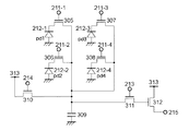
図2は、図1に示す撮像素子103の回路構成の一例を示す図である。撮像素子103の各画素は、水平2つ、垂直2つの計4つのフォトダイオードが、1つのマイクロレンズを共有する構成を有する。以下、この4つのフォトダイオードからなる画素を、分割画素と呼ぶ。図2は説明の簡略化のため、左上端4つの分割画素の構造のみを示しているが、実際には、多数の分割画素が2次元に配置されている。
FIG. 2 is a diagram illustrating an example of a circuit configuration of the
図2において、瞳分割方向指示入力104−1、水平同期信号(HD)入力104−2、垂直同期信号(VD)入力104−3、指示情報更新信号入力104−4は、撮像素子駆動部104から出力される。204はタイミング信号発生回路(TG)、205は第1のバッファ、207は第2のバッファ、209は画素読み出し共通制御信号バス、210は画素読み出し制御修正回路である。
In FIG. 2, the pupil division direction instruction input 104-1, the horizontal synchronization signal (HD) input 104-2, the vertical synchronization signal (VD) input 104-3, and the instruction information update signal input 104-4 are the image
211は画素読み出し制御信号バスである。また、212はマイクロレンズを共有する4つのフォトダイオードから成る分割画素を示し、212−1は第1のフォトダイオード、212−2は第2のフォトダイオード、212−3は第3のフォトダイオード、212−4は第4のフォトダイオードである。そして、画素読み出し制御信号バス211は、各分割画素212の第1〜第4のフォトダイオード212−1〜4の読み出しを制御する第1〜第4の読み出し制御信号211−1、211−2、211−3、211−4で構成される4つの制御信号を供給する。
また、213は分割画素212における行読み出し制御信号線、214はリセット信号線である。215は列読み出し信号線、216は水平駆動制御信号線、217は水平読み出し回路、103−1は第1の出力端子、103−2は第2の出力端子である。
図3は、図2の分割画素212の回路構成例を示すものである。図3において、305は第1の画素読み出しトランジスタ、306は第2の画素読み出しトランジスタ、307は第3の画素読み出しトランジスタ、308は第4の画素読み出しトランジスタである。また、また、309はフローティングディフュージョン部、310は画素リセットトランジスタ、311は行読み出しトランジスタ、312は画素ソースフォロワ、313は電源線である。
FIG. 3 shows a circuit configuration example of the divided
ここで、上記構成を有する分割画素212の加算読み出し手順について、図4を参照して説明する。図4(a)に示すタイミングチャートは、水平方向に瞳分割する場合の分割画素212の駆動制御を説明する図である。
Here, the addition reading procedure of the divided
まず、期間t31及び期間t32において、第1の画素読み出し制御信号211−1と第2の画素読み出し制御信号211−2を順にHighとする。これにより、第1の画素読み出しトランジスタ305と第2の画素読み出しトランジスタ306が順に導通する。その結果、第1のフォトダイオード212−1と第2のフォトダイオード212−2に蓄積された電荷が順次フローティングディフュージョン309に溜められて、電荷の加算が行われる。
First, in the period t31 and the period t32, the first pixel readout control signal 211-1 and the second pixel readout control signal 211-2 are sequentially set to High. As a result, the first
次に、期間t33において、行読み出し制御信号線213をHighとする。これにより、行読み出しトランジスタ311が導通し、画素ソースソースフォロワ312でフローティングディフュージョン309に溜められた加算電荷が電圧変換され、列読み出し信号線215を介して出力される。
Next, in a period t33, the row reading
次に、期間t34において、画素リセット制御信号214をHighとする。これにより、画素リセットトランジスタ310が導通し、フローティングディフュージョン309の電荷が0にリセットされる。
Next, in a period t34, the pixel reset
そして、期間t35及び期間36において、第3の画素読み出し制御信号211−3と第4の画素読み出し制御信号211−4を順にHighとする。これにより、第3の画素読み出しトランジスタ307と第4の画素読み出しトランジスタ308が順に導通する。その結果、第3のフォトダイオード212−3と第4のフォトダイオード212−4に蓄積された電荷が順次フローティングディフュージョン309に溜められて、電荷の加算が行われる。
Then, in the period t35 and the period 36, the third pixel readout control signal 211-3 and the fourth pixel readout control signal 211-4 are sequentially set to High. Thereby, the third
次に、期間t37において、期間t33と同様に、行読み出し制御信号線213をHighとすることで、フローティングディフュージョン309に溜められた加算電荷が電圧変換され、列読み出し信号線215を介して出力される。
Next, in the period t37, as in the period t33, the row readout
最後に、期間t38において、画素リセット制御信号214及び、全ての画素読み出し制御信号をHighとする。これにより、画素リセットトランジスタ310及び、全ての画素読み出しトランジスタが導通し、全てのフォトダイオード及びフローティングディフュージョン309の蓄積電荷はすべて0にリセットされ、次の読み出し駆動に対して、改めて光電荷の蓄積を行う。
Finally, in the period t38, the pixel reset
以上のようにして加算読み出しを行うことで、水平方向に瞳分割された左右画像の画像信号が読みだされる。 By performing addition reading as described above, the image signals of the left and right images divided in the horizontal direction are read out.
図4(b)は、垂直方向に瞳分割する場合の、分割画素212の駆動制御のタイミングチャートである。
FIG. 4B is a timing chart of drive control of the divided
なお、図4(b)の動作は、期間t31、t32、t35、t36における、第1〜第4の画素読み出し制御信号211−1〜4をHighとする組み合わせが、図4(a)のタイミングチャートと異なるだけである。そのため、図4(b)の詳細説明は省略する。図4(a)に示す動作との差異としては、図4(b)では、期間t32及び期間t33において、第1の画素読み出し制御信号211−1と第3の画素読み出し制御信号211−3を順次Highとなるようにする。そして、期間t36及び期間t37において、第2の画素読み出し制御信号211−2と第4の画素読み出し制御信号211−4が順次Highになるようにした点にある。 Note that in the operation of FIG. 4B, the combination of setting the first to fourth pixel readout control signals 211-1 to 21-4 to High in the periods t31, t32, t35, and t36 is the timing of FIG. It is only different from the chart. Therefore, the detailed description of FIG. As a difference from the operation illustrated in FIG. 4A, in FIG. 4B, in the period t32 and the period t33, the first pixel readout control signal 211-1 and the third pixel readout control signal 211-3 are changed. Set to high sequentially. Then, in the period t36 and the period t37, the second pixel readout control signal 211-2 and the fourth pixel readout control signal 211-4 are sequentially set to High.
以上のようにして加算読み出しを行うことで、垂直方向に瞳分割された上下画像の画像信号が読みだされる。 By performing addition reading as described above, the image signals of the upper and lower images divided in the vertical direction are read out.
なお、電圧変換された加算電荷は、水平読み出し回路217に入力される。本実施の形態の水平読み出し回路217は、先に読み出された画素信号と、後に読み出された画素信号を同時に読み出すように駆動することができる。従って、第1の出力端子103−1からは、左信号、もしくは上信号が出力され、第2の出力端子103−2からは、右信号、もしくは下信号が順次出力される。
The voltage-converted added charge is input to the
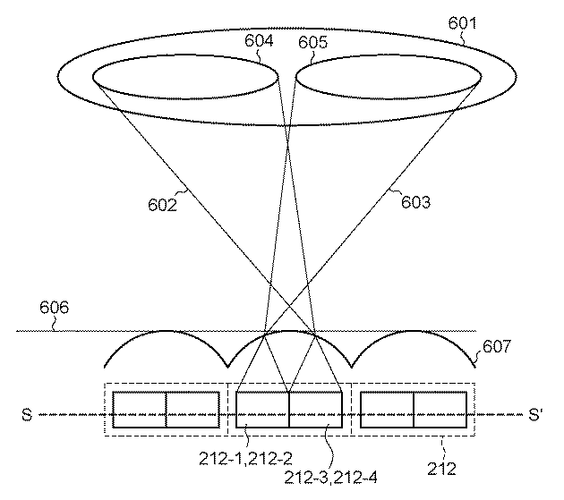
ここで、画像信号に基づく位相差評価値の算出方法について説明する。図5は、図2のS−S’間の断面を模式的に示したものである。601は、像側から見た撮像レンズの射出瞳を示したものである。合焦時の撮像レンズの結像面606から射出瞳601までの距離を射出瞳位置と呼び、図示していないレンズの絞りよりも後方(結像面側)にあるレンズ群の曲率や絞りとの位置関係などによりその位置は変化する。また、当然ながら絞りの径によって大きさは変化する。604、605はそれぞれマイクロレンズ607によって射出瞳位置に投影された第1及び第2のフォトダイオード212−1、212−2、及び、第3及び第4のフォトダイオード212−3、212−4の射出瞳である。第1及び第2のフォトダイオード212−1、212−2へは、射出瞳605を通る光束603が入るように設計され、第3及び第4のフォトダイオード212−3、212−4へは、射出瞳604を通る光束602が入るように設計される。また、撮像素子103を構成する他の分割画素についても同様に設計されており、各分割画素の第1及び第2のフォトダイオード212−1、212−2からは、撮像レンズの射出瞳601のうち右側の605の領域で見た像が得られる。同様に、各分割画素の第3及び第4のフォトダイオード212−3、212−4からは、撮像レンズの射出瞳601のうち左側の604の領域で見た像が得られる。光束602によって撮像素子103上で得られる像をA像、光束603によって撮像素子103上で得られる像をB像とすると、合焦状態によっては画像信号上に視差を含んだ信号が得られる。
Here, a method of calculating the phase difference evaluation value based on the image signal will be described. FIG. 5 schematically shows a cross section between S-S ′ in FIG. 2.
図6は、前ピン状態での画像信号の一例として、第3及び第4のフォトダイオード212−3、212−4で得られる像をA像702、第1及び第2のフォトダイオード212−1、212−2で得られる像をB像701として示している。位相差検出方式による被写体までの距離情報は、A像702とB像701の相対関係と像間の距離703、及び、そのフォーカス位置における結像面から射出瞳までの距離から算出される。位相差算出部109は、被写体までの距離情報を、算出した位相差評価値として、AF制御部110へ渡す。
FIG. 6 shows an image obtained by the third and fourth photodiodes 212-3 and 212-4 as an example of an image signal in the front pin state, an
位相差算出部109からの位相差評価値に基づいて、AF制御部110は目標フォーカス位置を決定し、現在のフォーカス位置からの移動方向及び移動量をフォーカス情報として、光学系駆動部102に渡す。
Based on the phase difference evaluation value from the phase
なお、上記説明では、水平方向に瞳分割して読み出された画像信号(右画像と左画像)から位相差評価値を算出する場合を示したが、垂直方向に瞳分割して読み出された画像信号(上画像と下画像)においても同様に実施可能であるため、説明を割愛する。 In the above description, the case where the phase difference evaluation value is calculated from the image signals (right image and left image) read out by dividing the pupil in the horizontal direction has been described. Since this can be similarly applied to the image signals (upper image and lower image), the description is omitted.
次に、本実施の形態における瞳分割方向指示情報の生成方法について説明する。本実施の形態における撮像装置では、撮像素子103から出力された画像信号を複数の分割領域に分割し、分割した分割領域毎に、分割画素の瞳分割方向を決定する。
Next, a method for generating pupil division direction instruction information in the present embodiment will be described. In the imaging apparatus according to the present embodiment, the image signal output from the
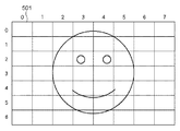
画像解析部107は、加算信号処理部105から出力される加算画像信号に対して画像解析を行い、指示情報生成部108に入力するための被写体情報を生成する。本実施の形態における被写体情報とは、図7に示すように、所定のサイズに分割された分割領域501毎の被写体の画像のエッジ方向の情報である。分割領域は、分割領域アドレス(i, j)で識別されるものとし、図7に示す例では、i = 0〜7、j = 0〜6の整数である。加算画像信号のアドレス(x, y)とは、下記の関係式(1)が成り立つ。なお、iとxは、水平方向のアドレスであり、jとyは垂直方向のアドレスである。
x = i × HSIZE + x'
y = j × VSIZE + y' …(1)
The
x = i × HSIZE + x '
y = j x VSIZE + y '(1)
ここで、x’とy’は、各分割領域内における加算画素信号の水平方向及び垂直方向のアドレスであり、HSIZE及びVSIZEは分割領域の水平方向及び垂直方向のサイズを示す。
画像解析部107には、分割領域アドレス(i, j)と加算画像信号のアドレス(x, y)とが共に入力される。まず、画像解析部107による分割領域毎の被写体情報(被写体の画像のエッジ方向の情報)の生成方法について説明する。
Here, x ′ and y ′ are horizontal and vertical addresses of the added pixel signal in each divided area, and HSIZE and VSIZE indicate the horizontal and vertical sizes of the divided areas.
The divided area address (i, j) and the address (x, y) of the added image signal are input to the
図8は、画像解析部107の構成を示すブロック図である。図8において、401は、加算信号処理部105が生成した加算画像信号から水平方向の勾配値を算出する水平微分フィルタであり、403は、水平方向の勾配値を絶対値化する絶対値化部である。402は、加算画像信号から垂直方向の勾配値を算出する垂直微分フィルタであり、404は、垂直方向の勾配値を絶対値化する絶対値化部である。
FIG. 8 is a block diagram illustrating a configuration of the
405は、画素毎の水平方向の勾配値の絶対値と垂直方向の勾配値の絶対値の大小判定を行う大小判定部である。406は、分割領域毎に含まれる画素毎の大小判定結果の統計をとる分割領域統計部である。407は、分割領域の統計情報とその周囲の分割領域の統計情報に基づいて、分割領域のエッジ方向を判定するエッジ方向判定部である。408は、分割領域の統計情報を記憶する記憶部である。
図9は。画像解析部107による、着目分割領域(i, j)のエッジ方向決定処理を示す図9のフローチャートである。
FIG. FIG. 10 is a flowchart of FIG. 9 showing edge direction determination processing of the target divided region (i, j) by the
加算画像信号は分割領域単位で入力され、分割領域毎に統計処理を行うので、分割領域単位の処理設定を初期化する(S11)。次に、加算画像信号は、水平方向の水平微分フィルタ401、及び垂直方向の垂直微分フィルタ402に入力され、加算画素信号毎に勾配値が算出される。この微分フィルタは、例えば、既知のSobelフィルタで構成することができる。加算画素信号毎に求められた水平方向、及び垂直方向の勾配値は、それぞれ絶対値化部403、404に入力され、絶対値化される(S12)。
The added image signal is input for each divided region, and statistical processing is performed for each divided region, so that the processing setting for each divided region is initialized (S11). Next, the added image signal is input to a horizontal
絶対値化された加算画素毎の水平方向及び垂直方向の勾配値は、大小判定部405で大小判定が行われ、水平方向の勾配値の絶対値が垂直方向の勾配値の絶対値より大きければ0、そうでなければ1を判定情報として出力する(S13)。
The magnitude values in the horizontal direction and the vertical direction for each added pixel that have been converted into absolute values are determined by the
大小判定部405から出力される判定情報は、分割領域統計部406に入力される。分割領域統計部406は、まず、判定情報が着目分割領域内の加算画像信号のものであるかを判定する(S14でYES)。分割領域統計部406には、判定情報と同時に加算画像信号のアドレスが入力されるので、加算画像信号アドレス(x, y)が、着目分割領域(i, j)内であれば、着目分割領域の判定情報とみなす。なお、着目領域内か否かの判定は、下記式(2)によって表現される。
i × HSIZE ≦ x < (i + 1) × HSIZE
j × VSIZE ≦ y < (i + 1) × VSIZE …(2)
The determination information output from the
i × HSIZE ≤ x <(i + 1) × HSIZE
j x VSIZE ≤ y <(i + 1) x VSIZE (2)
分割領域統計部406は、判定情報である0と1、各々の出現個数をカウントする、カウンタC0とカウンタC1で構成される。入力画素の判定情報が0であればカウンタC0を1増加し、判定情報が1であればカウンタC1を1増加する(S15)。着目分割領域内の加算画素信号の判定情報が全て入力されると(S14でNO)、分割領域統計部406は、カウンタC0とカウンタC1の値を統計情報として出力する。統計情報は、カウンタC0>カウンタC1であれば、着目分割領域の水平方向の勾配が大きい、つまりエッジ方向は垂直であることを示す。そうでなければ、着目分割領域の垂直方向の勾配が大きい、つまりエッジ方向は水平であることを示す。
The divided
図10は、分割領域統計部406により求められた、着目分割領域502の統計情報から推定されるエッジ方向の一例を示す図である。図10(a)は、着目分割領域502における統計情報を示しており、カウンタC0>カウンタC1である。この場合、図10(b)に示すように、着目分割領域502のエッジ方向は垂直であることを示している。しかしながら、本実施の形態では、着目分割領域のエッジ方向を、着目分割領域の統計情報からだけではなく、着目分割領域の周囲の分割領域の統計情報も用いて決定する。
FIG. 10 is a diagram illustrating an example of the edge direction estimated from the statistical information of the target divided
分割領域統計部406から出力される統計情報は、エッジ方向判定部407と記憶部408に入力される。記憶部408は例えばSRAMで構成され、分割領域毎の統計情報を全て保持する。そして、入力される着目分割領域アドレスより、その周囲8方向の分割領域それぞれの統計情報を、エッジ方向判定部407に出力する(S16)。
Statistical information output from the divided region
エッジ方向判定部407は、着目分割領域(i, j)の統計領域と、記憶部408に予め記憶された周囲8方向の分割領域の統計情報とを用いて、最終的な着目分割領域(i, j)のエッジ方向判定を行う(S17)。ここでは、着目分割領域(i, j)のカウンタC0の値C0(i, j)及び周囲の分割領域のカウンタC0の値を、以下の式(3)により重み付け合成し、その合成値C0’を着目分割領域(i, j)の最終的な水平方向の勾配情報とする。
The edge
同様に着目分割領域(i, j)のカウンタC1の値C1(i, j)及び周囲の分割領域のカウンタC1の値を、以下の式(4)により重み付け合成し、その合成値C1’を着目分割領域(i, j)の最終的な垂直方向の勾配情報とする。 Similarly, the value C1 (i, j) of the counter C1 of the target divided region (i, j) and the value of the counter C1 of the surrounding divided region are weighted and synthesized by the following equation (4), and the synthesized value C1 ′ is obtained. The gradient information in the final vertical direction of the target divided region (i, j) is used.
そして、合成値C0’と合成値C1’の大小比較を行い、合成値C0’>合成値C1’であれば、着目分割領域(i, j)のエッジ方向は垂直(第1の方向)であると判定し、被写体情報を0として出力する。合成値C0’>合成値C1’でなければ、エッジ方向は水平(第2の方向)であると判定し、被写体情報を1として出力する(S17)。
図11は、着目分割領域502で求められた統計情報と、その周囲の分割領域503の統計情報から決定したエッジ方向の一例を示す図である。図11(a)は、着目分割領域502、及びその周囲の着目分割領域群503の統計情報を示しており、式(3)及び式(4)に基づいて合成値を算出すると、合成値C1’>合成値C0’である。そのため、図11(b)に示すように、合成値の関係から、エッジ方向判定部407は、着目分割領域502のエッジ方向は水平であると判定する。
Then, the composite value C0 ′ and the composite value C1 ′ are compared in magnitude. If the composite value C0 ′> the composite value C1 ′, the edge direction of the target divided region (i, j) is vertical (first direction). It is determined that there is, and the subject information is output as 0. If the composite value C0 ′> the composite value C1 ′ is not satisfied, it is determined that the edge direction is horizontal (second direction), and the subject information is output as 1 (S17).
FIG. 11 is a diagram illustrating an example of the edge direction determined from the statistical information obtained in the target divided
そして、指示情報生成部108は、エッジ方向判定部407から出力された被写体情報が0、即ち、エッジ方向が垂直(第1の方向)の場合、対応する分割領域に含まれる各分割画素の瞳分割方向を水平方向(第1の瞳分割方向)とする。そして、瞳分割方向指示情報として「0」を出力する。また、エッジ方向判定部407から出力された被写体情報が1、即ち、エッジ方向が水平(第2の方向)の場合、対応する分割領域に含まれる各分割画素の瞳分割方向を垂直方向(第2の瞳分割方向)とする。そして、瞳分割方向指示情報として「1」を出力する。何れの場合も、分割領域アドレスを加算画像信号アドレスに変換することで、各分割画素の瞳分割方向を指定することができる。
Then, when the subject information output from the edge
このようにして指示情報生成部108から出力された瞳分割方向指示情報は、撮像素子駆動部104へは、行毎に入力され、位相差算出部109へは、分割領域毎に入力される。位相差算出部109に渡す瞳分割方向指示情報は、現在読み出されている画像信号に対するものであるため、メモリなどの記憶部に分割領域毎の瞳分割指示情報を記憶させ、撮像素子103に設定される瞳分割方向指示情報とタイミングを合わせる必要がある。
The pupil division direction instruction information output from the instruction
なお、上述した例では、着目分割領域のエッジ方向を、着目分割領域とその周辺分割領域のエッジ方向とから判定したが、着目分割領域のエッジ方向からのみに基づいて決定しても良い。その場合、エッジ方向判定部407は分割領域統計部406から出力されるカウンタC0及びカウンタC1の大小関係に基づいて、エッジ方向が垂直(第1の方向)であるか、水平(第2の方向)であるかを決定すればよい。
In the above-described example, the edge direction of the target divided region is determined from the target divided region and the edge directions of the peripheral divided regions, but may be determined based only on the edge direction of the target divided region. In this case, the edge
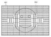
図12は、加算画像信号に対して、全分割領域にエッジ方向判定を行った結果の一例を示す図である。上述したようにして、分割領域毎に被写体の主要なエッジ方向を決定し、エッジ方向に適した瞳分割を行うことができるので、より精度の高い位相差評価値を得ることができ、ひいては、より精度の高い焦点調節処理を行うことができる。 FIG. 12 is a diagram illustrating an example of a result of edge direction determination performed on all divided regions with respect to the added image signal. As described above, the main edge direction of the subject can be determined for each divided region, and pupil division suitable for the edge direction can be performed, so that a more accurate phase difference evaluation value can be obtained. A more accurate focus adjustment process can be performed.
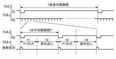
次に、上述したようにして得られた瞳分割指示情報を撮像素子駆動部104に設定するタイミングについて図13のタイミングチャートを参照して説明する。
Next, timing for setting the pupil division instruction information obtained as described above to the image
図2に示す瞳分割方向指示入力104−1には、指示情報生成手段かから出力された分割画素毎の瞳分割方向指示情報が0または1のディジタル信号として入力される。上述したように、0は水平方向の瞳分割を指定し、1は垂直方向の瞳分割を指定する。 In the pupil division direction instruction input 104-1 shown in FIG. 2, the pupil division direction instruction information for each divided pixel output from the instruction information generation unit is input as a digital signal of 0 or 1. As described above, 0 designates the pupil division in the horizontal direction, and 1 designates the pupil division in the vertical direction.
n行目の瞳分割方向指示情報は、水平駆動期間t2においてn−1行目の画像信号を読み出している間に、分割画素毎に入力され、第1のバッファ205にそれぞれ保持される。次に、瞳分割方向指示情報は、図13のn行目の水平ブランキング期間t3の初期において、指示情報更新信号入力104−4からの更新指示によって、第2のバッファ207へ保持される。これにより、1行分の瞳分割方向指示情報が同時に参照可能となり、画素読み出し制御修正回路210に入力される。
The pupil division direction instruction information on the n-th row is input for each divided pixel and is held in the
水平同期信号入力104−2と垂直同期信号入力104−3から入力された水平同期信号HDと垂直同期信号VDは、タイミング信号発生回路204に入力される。そして、これらの信号を基にして、タイミング信号発生回路204により、画素読み出し共通制御信号バス209及び行読み出し制御信号線213への制御信号が生成される。
The horizontal synchronization signal HD and the vertical synchronization signal VD input from the horizontal synchronization signal input 104-2 and the vertical synchronization signal input 104-3 are input to the timing
画素読み出し共通制御信号バス209の信号は、画素読み出し制御信号バス211の元となる制御信号である。図3で示したように、画素読み出し制御信号バス211は、各分割画素のフォトダイオードの読み出し制御信号211−1、211−2、211−3、211−4で構成される4つの制御信号を供給するバスである。これらは、画素読み出し制御修正回路210に入力され、1行分の瞳分割方向指示情報に従い、各修正回路210毎に、画素読み出し共通制御信号バス209の制御信号を修正する動作をする。本実施の形態では、瞳分割方向指示情報が0(水平方向)の場合は、画素読み出し共通制御信号バス209の信号をそのまま通過させ、図3(a)で説明したような電荷の加算が行われるように分割画素からの読み出しを制御する。一方、瞳分割方向指示情報が1(垂直方向)の場合は、画素読み出し共通制御信号バス209の信号を修正し、図3(b)で説明したような電荷の加算が行われるように分割画素からの読み出しを制御する。
A signal on the pixel readout common
そして、水平駆動期間t4において、瞳分割方向指示情報に応じて瞳分割されたn行目の信号を読み出す。また、この水平駆動期間t4に、次のn+1行目の瞳分割指示情報を第1のバッファ205にそれぞれ保持しておく。以上の動作を繰り返すことにより、1垂直同期期間内の画像信号の読み出し処理が終了する。
Then, in the horizontal driving period t4, the n-th row signal read out in accordance with the pupil division direction instruction information is read out. Further, during the horizontal drive period t4, the pupil division instruction information for the next (n + 1) th row is held in the
以上説明したように、本実施の形態における撮像素子103において、第1の出力端子103−1からは、入力された瞳分割方向指示情報に応じて、左画像または上画像が出力され、第2の出力端子103−2からは右画像または下画像が出力される。
As described above, in the
このようにして撮像素子103から得られた瞳分割された対の画像信号は、位相差算出部109へ入力される一方、加算信号処理部105へも入力され、カメラ信号処理部106や、画像解析部107に入力する加算画像信号が生成される。即ち、加算信号処理部105は、第1の出力端子103−1と第2の出力端子103−2から出力される、左画像信号と右画像信号、もしくは上画像信号と下画像信号を加算して、加算画像信号を生成する。
The pair of pupil-divided image signals obtained from the
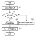
次に、本実施の形態のフォーカス情報生成処理について、図14のフローチャートを参照して説明する。 Next, focus information generation processing according to the present embodiment will be described with reference to the flowchart of FIG.
まず、位相差算出部109より、指示情報生成部108から分割領域毎に入力された瞳分割方向指示情報に従って、図6で説明したようにして、分割領域毎に水平方向または垂直方向の位相差評価値を取得する(S21)。次に、焦点調節の対象となる被写体の有無を判定する(S22)。なお、焦点調節の対象となる被写体の有無の判定方法としては、例えば、顔検出などの既知の被写体検出処理などがある。被写体検出処理では、焦点調節の対象となる被写体の有無判定と、その位置及びサイズ情報を算出する。
First, in accordance with the pupil division direction instruction information input from the instruction
焦点調節の対象となる被写体が存在する場合は(S22でYES)、その位置とサイズ情報とから、その被写体が存在する分割領域群をフォーカス情報取得に用いる分割領域として設定する(S23)。一方、焦点調節の対象となる被写体が存在しなかった場合は、例えば、画面中央などの、予め設定された分割領域群をフォーカス情報取得に用いる分割領域として設定する(S24)。 If there is a subject to be focused (YES in S22), a divided region group in which the subject exists is set as a divided region used for focus information acquisition from the position and size information (S23). On the other hand, when there is no subject for focus adjustment, for example, a preset divided region group such as the center of the screen is set as a divided region used for focus information acquisition (S24).
そして、AF制御部110は、S23またはS24で指定された分割領域群の位相差評価値の最大値を被写体までの距離情報とし、フォーカス情報を算出する。
Then, the
上記の通り本実施の形態によれば、撮像素子103の各画素の複数のフォトダイオードそれぞれから独立に読み出す場合と比較して、読み出す信号数を半減することで、システム負荷を低減することができる。また、被写体のエッジ方向に合わせて、分割領域毎に瞳分割方向を変えて画像信号を出力することができるため、合焦対象の被写体に適した位相差評価値を得ることができ、位相差方式の焦点調節制御の精度を高めることができる。
As described above, according to the present embodiment, it is possible to reduce the system load by halving the number of signals to be read as compared to the case where the pixels of the
なお、上述した実施の形態では、全ての画素が4つのフォトダイオードにより構成されているものとして説明したが、本発明はこれに限るものではなく、例えば、撮像素子103の画面内において、通常の画素の中に離散的に配置してもよい。
In the above-described embodiment, it has been described that all the pixels are configured by four photodiodes. However, the present invention is not limited to this. For example, in the screen of the
また、上述した実施の形態では、各分割領域のエッジ方向が水平であるか垂直であるかを判定してから、判定結果に基づいて瞳分割方向を決定する場合について説明した。しかしながら、本発明はこれに限るものではなく、カウンタC0とカウンタC1との値をもってエッジ方向とし、これらの値に基づいて、瞳分割方向を決定しても良い。 Further, in the above-described embodiment, a case has been described in which it is determined whether the edge direction of each divided region is horizontal or vertical, and then the pupil division direction is determined based on the determination result. However, the present invention is not limited to this, and the edge direction may be determined based on the values of the counter C0 and the counter C1, and the pupil division direction may be determined based on these values.
また、エッジ方向の判定方法は上述したものに限るものではなく、エッジ方向が判定できるのであれば、どのような方法を用いても構わない。そして、エッジ方向の傾斜の度合いに基づいて、効果的な位相差を得ることができる瞳分割方向を決定するようにすればよい。すなわち、エッジ方向がより水平に近ければ、瞳分割方向を垂直とし、エッジ方向がより垂直に近ければ、瞳分割方向を水平とすればよい。 Further, the edge direction determination method is not limited to the above-described method, and any method may be used as long as the edge direction can be determined. Then, a pupil division direction that can obtain an effective phase difference may be determined based on the degree of inclination in the edge direction. That is, if the edge direction is closer to the horizontal, the pupil division direction may be vertical, and if the edge direction is closer to the vertical, the pupil division direction may be horizontal.
Claims (8)
前記撮像素子から読み出した電荷から得られた画素毎の画像信号に基づいて、前記撮像素子の領域を複数に分割した分割領域毎に画像のエッジの方向を判定する判定手段と、
前記判定手段により前記分割領域毎に判定されたエッジの方向に基づいて、前記分割領域毎に、前記第1の瞳分割方向と前記第2の瞳分割方向の何れかを決定する決定手段と、
前記決定手段により決定された前記第1の瞳分割方向または前記第2の瞳分割方向に分割して、前記各分割画素の加算読み出しを行い、対の画像信号を出力するように前記撮像素子を制御する読み出し制御手段と、
前記読み出し制御手段による制御により前記各分割画素から出力された対の画像信号の位相差に基づいて、焦点調節を行う焦点調節手段と
を有することを特徴とする撮像装置。 A plurality of divided pixels each including a plurality of two-dimensionally arranged photoelectric conversion units that respectively receive light beams that have passed through different regions of the exit pupil of the optical system, and a first pupil division for each of the divided pixels; An image sensor capable of adding and reading the generated charges by dividing the photoelectric conversion unit in a direction and a second pupil division direction perpendicular to the first pupil division direction;
Determination means for determining the direction of the edge of the image for each divided region obtained by dividing the region of the image sensor based on an image signal for each pixel obtained from the charge read from the image sensor;
Determining means for determining, for each of the divided regions, either the first pupil dividing direction or the second pupil dividing direction based on the edge direction determined for each of the divided regions by the determining unit;
The imaging device is divided so as to divide in the first pupil division direction or the second pupil division direction determined by the determination means, perform addition reading of each divided pixel, and output a pair of image signals. Read control means for controlling;
An image pickup apparatus comprising: a focus adjustment unit that performs focus adjustment based on a phase difference between a pair of image signals output from each of the divided pixels under the control of the readout control unit.
判定手段が、前記撮像素子から読み出した電荷から得られた画素毎の画像信号に基づいて、前記撮像素子の領域を複数に分割した分割領域毎に画像のエッジの方向を判定する判定工程と、
決定手段が、前記判定工程で前記分割領域毎に判定されたエッジの方向に基づいて、前記分割領域毎に、前記第1の瞳分割方向と前記第2の瞳分割方向の何れかを決定する決定工程と、
読み出し制御手段が、前記決定工程で決定された前記第1の瞳分割方向または前記第2の瞳分割方向に分割して、前記各分割画素の加算読み出しを行い、対の画像信号を出力するように前記撮像素子を制御する読み出し制御工程と、
焦点調節手段が、前記読み出し制御工程による制御により前記各分割画素から出力された対の画像信号の位相差に基づいて、焦点調節を行う焦点調節工程と
を有することを特徴とする撮像装置の制御方法。 A plurality of divided pixels each including a plurality of two-dimensionally arranged photoelectric conversion units that respectively receive light beams that have passed through different regions of the exit pupil of the optical system, and a first pupil division for each of the divided pixels; A control method of an imaging apparatus having an imaging element capable of adding and reading generated charges by dividing the photoelectric conversion unit in a direction and a second pupil division direction perpendicular to the first pupil division direction,
A determination step of determining a direction of an edge of the image for each divided region obtained by dividing the region of the image sensor based on an image signal for each pixel obtained from the charge read from the image sensor;
The determining means determines either the first pupil division direction or the second pupil division direction for each of the divided regions based on the edge direction determined for each of the divided regions in the determination step. A decision process;
A readout control unit divides in the first pupil division direction or the second pupil division direction determined in the determination step, performs addition reading of each of the divided pixels, and outputs a pair of image signals. A readout control step for controlling the image sensor;
The focus adjustment unit has a focus adjustment step of performing focus adjustment based on the phase difference between the pair of image signals output from each of the divided pixels by the control in the readout control step. Method.
Priority Applications (2)
| Application Number | Priority Date | Filing Date | Title |
|---|---|---|---|
| JP2011015706A JP5856376B2 (en) | 2011-01-27 | 2011-01-27 | Imaging apparatus and control method thereof |
| US13/352,945 US8749697B2 (en) | 2011-01-27 | 2012-01-18 | Image capturing apparatus and control method thereof |
Applications Claiming Priority (1)
| Application Number | Priority Date | Filing Date | Title |
|---|---|---|---|
| JP2011015706A JP5856376B2 (en) | 2011-01-27 | 2011-01-27 | Imaging apparatus and control method thereof |
Publications (3)
| Publication Number | Publication Date |
|---|---|
| JP2012155221A true JP2012155221A (en) | 2012-08-16 |
| JP2012155221A5 JP2012155221A5 (en) | 2014-03-13 |
| JP5856376B2 JP5856376B2 (en) | 2016-02-09 |
Family
ID=46577076
Family Applications (1)
| Application Number | Title | Priority Date | Filing Date |
|---|---|---|---|
| JP2011015706A Active JP5856376B2 (en) | 2011-01-27 | 2011-01-27 | Imaging apparatus and control method thereof |
Country Status (2)
| Country | Link |
|---|---|
| US (1) | US8749697B2 (en) |
| JP (1) | JP5856376B2 (en) |
Cited By (4)
| Publication number | Priority date | Publication date | Assignee | Title |
|---|---|---|---|---|
| WO2016111175A1 (en) * | 2015-01-07 | 2016-07-14 | ソニー株式会社 | Image processing device, image processing method, and program |
| JPWO2017169479A1 (en) * | 2016-03-31 | 2019-01-31 | 株式会社ニコン | IMAGING ELEMENT AND IMAGING DEVICE |
| JP2020141206A (en) * | 2019-02-27 | 2020-09-03 | キヤノン株式会社 | Imaging element, imaging apparatus, and control method of imaging element |
| WO2021158043A1 (en) * | 2020-02-04 | 2021-08-12 | 삼성전자 주식회사 | Electronic device, and method for performing autofocus |
Families Citing this family (14)
| Publication number | Priority date | Publication date | Assignee | Title |
|---|---|---|---|---|
| EP2833623B1 (en) * | 2012-03-30 | 2019-09-18 | Nikon Corporation | Image sensor, imaging method, and imaging device |
| JP5833254B2 (en) * | 2012-11-14 | 2015-12-16 | 富士フイルム株式会社 | Image processing apparatus, imaging apparatus, image processing method, and image processing program |
| JP2014106476A (en) | 2012-11-29 | 2014-06-09 | Canon Inc | Focus detection device, imaging device, imaging system, focus detection method, program and storage medium |
| JP6346439B2 (en) * | 2013-01-07 | 2018-06-20 | キヤノン株式会社 | Imaging apparatus and control method thereof |
| US20140362190A1 (en) * | 2013-06-07 | 2014-12-11 | Canon Kabushiki Kaisha | Depth measurement apparatus, imaging apparatus, and method of controlling depth measurement apparatus |
| US9402069B2 (en) * | 2013-06-07 | 2016-07-26 | Canon Kabushiki Kaisha | Depth measurement apparatus, imaging apparatus, and method of controlling depth measurement apparatus |
| JP6207243B2 (en) * | 2013-06-07 | 2017-10-04 | キヤノン株式会社 | Ranging device, imaging device, and control method of ranging device |
| US9354212B2 (en) * | 2014-01-07 | 2016-05-31 | Applied Materials Israel Ltd. | Inspection having a segmented pupil |
| JP2016038414A (en) * | 2014-08-05 | 2016-03-22 | キヤノン株式会社 | Focus detection device, control method thereof, and imaging apparatus |
| JP6553881B2 (en) * | 2015-02-05 | 2019-07-31 | キヤノン株式会社 | Image processing device |
| US9787889B2 (en) * | 2015-02-12 | 2017-10-10 | Semiconductor Components Industries, Llc | Dynamic auto focus zones for auto focus pixel systems |
| KR20170056909A (en) * | 2015-11-16 | 2017-05-24 | 삼성전자주식회사 | Image sensor and electronic device having the same |
| JP6727017B2 (en) * | 2016-04-21 | 2020-07-22 | キヤノン株式会社 | IMAGING DEVICE AND ITS CONTROL METHOD, IMAGE PROCESSING DEVICE, AND IMAGE PROCESSING METHOD |
| JP2017195584A (en) * | 2016-04-22 | 2017-10-26 | キヤノン株式会社 | Imaging apparatus |
Citations (5)
| Publication number | Priority date | Publication date | Assignee | Title |
|---|---|---|---|---|
| JP2002314062A (en) * | 2001-04-18 | 2002-10-25 | Canon Inc | Solid-state image sensing device and image sensing system |
| JP2007103590A (en) * | 2005-10-03 | 2007-04-19 | Nikon Corp | Image pick-up device, focus detector and image pick-up system |
| JP2007325139A (en) * | 2006-06-03 | 2007-12-13 | Nikon Corp | Solid-state image pickup element and imaging apparatus using the same |
| JP2009094881A (en) * | 2007-10-10 | 2009-04-30 | Nikon Corp | Imaging apparatus and imaging method |
| JP2010020016A (en) * | 2008-07-09 | 2010-01-28 | Canon Inc | Image pick up apparatus |
Family Cites Families (3)
| Publication number | Priority date | Publication date | Assignee | Title |
|---|---|---|---|---|
| JP4770560B2 (en) * | 2006-04-11 | 2011-09-14 | 株式会社ニコン | Imaging apparatus, camera, and image processing method |
| JP2011039499A (en) * | 2009-07-14 | 2011-02-24 | Hoya Corp | Automatic focus detection device |
| JP5753371B2 (en) * | 2010-11-25 | 2015-07-22 | キヤノン株式会社 | Imaging apparatus and control method thereof |
-
2011
- 2011-01-27 JP JP2011015706A patent/JP5856376B2/en active Active
-
2012
- 2012-01-18 US US13/352,945 patent/US8749697B2/en active Active
Patent Citations (5)
| Publication number | Priority date | Publication date | Assignee | Title |
|---|---|---|---|---|
| JP2002314062A (en) * | 2001-04-18 | 2002-10-25 | Canon Inc | Solid-state image sensing device and image sensing system |
| JP2007103590A (en) * | 2005-10-03 | 2007-04-19 | Nikon Corp | Image pick-up device, focus detector and image pick-up system |
| JP2007325139A (en) * | 2006-06-03 | 2007-12-13 | Nikon Corp | Solid-state image pickup element and imaging apparatus using the same |
| JP2009094881A (en) * | 2007-10-10 | 2009-04-30 | Nikon Corp | Imaging apparatus and imaging method |
| JP2010020016A (en) * | 2008-07-09 | 2010-01-28 | Canon Inc | Image pick up apparatus |
Cited By (5)
| Publication number | Priority date | Publication date | Assignee | Title |
|---|---|---|---|---|
| WO2016111175A1 (en) * | 2015-01-07 | 2016-07-14 | ソニー株式会社 | Image processing device, image processing method, and program |
| JPWO2017169479A1 (en) * | 2016-03-31 | 2019-01-31 | 株式会社ニコン | IMAGING ELEMENT AND IMAGING DEVICE |
| JP2020141206A (en) * | 2019-02-27 | 2020-09-03 | キヤノン株式会社 | Imaging element, imaging apparatus, and control method of imaging element |
| JP7337512B2 (en) | 2019-02-27 | 2023-09-04 | キヤノン株式会社 | IMAGE SENSOR, IMAGING DEVICE, AND IMAGE SENSOR CONTROL METHOD |
| WO2021158043A1 (en) * | 2020-02-04 | 2021-08-12 | 삼성전자 주식회사 | Electronic device, and method for performing autofocus |
Also Published As
| Publication number | Publication date |
|---|---|
| US20120194721A1 (en) | 2012-08-02 |
| US8749697B2 (en) | 2014-06-10 |
| JP5856376B2 (en) | 2016-02-09 |
Similar Documents
| Publication | Publication Date | Title |
|---|---|---|
| JP5856376B2 (en) | Imaging apparatus and control method thereof | |
| JP2012155221A5 (en) | ||
| JP5850680B2 (en) | Imaging apparatus and control method thereof | |
| JP2017216646A (en) | Imaging device, imaging apparatus and imaging signal processing method | |
| US20160234425A1 (en) | Image processing apparatus | |
| JP6351231B2 (en) | IMAGING DEVICE, IMAGING SYSTEM, IMAGING DEVICE CONTROL METHOD, PROGRAM, AND STORAGE MEDIUM | |
| CN111669483B (en) | Image sensor, imaging device, electronic apparatus, image processing system, and signal processing method | |
| US10225494B2 (en) | Image capturing apparatus and control method thereof | |
| JP2013016999A (en) | Imaging apparatus and control method thereof | |
| US20180220058A1 (en) | Image capture apparatus, control method therefor, and computer-readable medium | |
| JP2015212794A (en) | Imaging device, control method of the same and control program | |
| JP6748477B2 (en) | Imaging device, control method thereof, program, and storage medium | |
| JP2015148676A (en) | Imaging apparatus and method of controlling imaging apparatus | |
| JP2017216649A (en) | Imaging device, imaging apparatus and imaging signal processing method | |
| US10122913B2 (en) | Image capturing apparatus and control method thereof, and storage medium | |
| US10551591B2 (en) | Imaging apparatus, control method of imaging apparatus, and storage medium storing control program of imaging apparatus for performing focus detection and display | |
| US11310410B2 (en) | Image capturing apparatus, method of controlling same, and storage medium | |
| JP6678505B2 (en) | Imaging device, control method therefor, program, and storage medium | |
| US10203206B2 (en) | Image capture apparatus having signal readouts using distance measurement region | |
| US10136088B2 (en) | Image pickup apparatus that reduces amount of information of defective pixels, method of controlling the same, and storage medium | |
| JP2017022639A (en) | Image processing apparatus, imaging apparatus and image processing program | |
| US20220385875A1 (en) | Device, capturing device, control method, and storage medium | |
| JP2014219545A (en) | Imaging apparatus, method of controlling the same, and control program | |
| US10904424B2 (en) | Image capturing apparatus | |
| JP2017034508A (en) | Image pickup device, control method thereof, and imaging apparatus |
Legal Events
| Date | Code | Title | Description |
|---|---|---|---|
| A521 | Request for written amendment filed |
Free format text: JAPANESE INTERMEDIATE CODE: A523 Effective date: 20140124 |
|
| A621 | Written request for application examination |
Free format text: JAPANESE INTERMEDIATE CODE: A621 Effective date: 20140124 |
|
| A977 | Report on retrieval |
Free format text: JAPANESE INTERMEDIATE CODE: A971007 Effective date: 20141121 |
|
| A131 | Notification of reasons for refusal |
Free format text: JAPANESE INTERMEDIATE CODE: A131 Effective date: 20141201 |
|
| A521 | Request for written amendment filed |
Free format text: JAPANESE INTERMEDIATE CODE: A523 Effective date: 20150130 |
|
| A131 | Notification of reasons for refusal |
Free format text: JAPANESE INTERMEDIATE CODE: A131 Effective date: 20150703 |
|
| A521 | Request for written amendment filed |
Free format text: JAPANESE INTERMEDIATE CODE: A523 Effective date: 20150831 |
|
| TRDD | Decision of grant or rejection written | ||
| A01 | Written decision to grant a patent or to grant a registration (utility model) |
Free format text: JAPANESE INTERMEDIATE CODE: A01 Effective date: 20151113 |
|
| A61 | First payment of annual fees (during grant procedure) |
Free format text: JAPANESE INTERMEDIATE CODE: A61 Effective date: 20151211 |
|
| R151 | Written notification of patent or utility model registration |
Ref document number: 5856376 Country of ref document: JP Free format text: JAPANESE INTERMEDIATE CODE: R151 |