JP2012151452A - Photodetector optimized by metal texturing provided on rear surface - Google Patents
Photodetector optimized by metal texturing provided on rear surface Download PDFInfo
- Publication number
- JP2012151452A JP2012151452A JP2011276876A JP2011276876A JP2012151452A JP 2012151452 A JP2012151452 A JP 2012151452A JP 2011276876 A JP2011276876 A JP 2011276876A JP 2011276876 A JP2011276876 A JP 2011276876A JP 2012151452 A JP2012151452 A JP 2012151452A
- Authority
- JP
- Japan
- Prior art keywords
- mirror
- electromagnetic radiation
- periodic grating
- absorption layer
- detector
- Prior art date
- Legal status (The legal status is an assumption and is not a legal conclusion. Google has not performed a legal analysis and makes no representation as to the accuracy of the status listed.)
- Pending
Links
- 229910052751 metal Inorganic materials 0.000 title claims abstract description 56
- 239000002184 metal Substances 0.000 title claims abstract description 56
- 239000004065 semiconductor Substances 0.000 claims abstract description 129
- 230000000737 periodic effect Effects 0.000 claims abstract description 90
- 238000010521 absorption reaction Methods 0.000 claims abstract description 70
- 230000005855 radiation Effects 0.000 claims abstract description 40
- 230000005670 electromagnetic radiation Effects 0.000 claims abstract description 32
- 239000000463 material Substances 0.000 claims abstract description 9
- 238000001465 metallisation Methods 0.000 claims description 32
- 238000001514 detection method Methods 0.000 claims description 19
- 229910000661 Mercury cadmium telluride Inorganic materials 0.000 claims description 16
- 239000000969 carrier Substances 0.000 claims description 16
- 229910052984 zinc sulfide Inorganic materials 0.000 claims description 14
- 239000010931 gold Substances 0.000 claims description 10
- 229910052732 germanium Inorganic materials 0.000 claims description 8
- GNPVGFCGXDBREM-UHFFFAOYSA-N germanium atom Chemical compound [Ge] GNPVGFCGXDBREM-UHFFFAOYSA-N 0.000 claims description 6
- PCHJSUWPFVWCPO-UHFFFAOYSA-N gold Chemical compound [Au] PCHJSUWPFVWCPO-UHFFFAOYSA-N 0.000 claims description 6
- 229910052737 gold Inorganic materials 0.000 claims description 6
- BQCADISMDOOEFD-UHFFFAOYSA-N Silver Chemical compound [Ag] BQCADISMDOOEFD-UHFFFAOYSA-N 0.000 claims description 5
- 230000003287 optical effect Effects 0.000 claims description 5
- 229910052709 silver Inorganic materials 0.000 claims description 5
- 239000004332 silver Substances 0.000 claims description 5
- 239000005083 Zinc sulfide Substances 0.000 claims description 4
- 229910052782 aluminium Inorganic materials 0.000 claims description 4
- XAGFODPZIPBFFR-UHFFFAOYSA-N aluminium Chemical compound [Al] XAGFODPZIPBFFR-UHFFFAOYSA-N 0.000 claims description 4
- DRDVZXDWVBGGMH-UHFFFAOYSA-N zinc;sulfide Chemical compound [S-2].[Zn+2] DRDVZXDWVBGGMH-UHFFFAOYSA-N 0.000 claims description 4
- RYGMFSIKBFXOCR-UHFFFAOYSA-N Copper Chemical compound [Cu] RYGMFSIKBFXOCR-UHFFFAOYSA-N 0.000 claims description 3
- 229910000530 Gallium indium arsenide Inorganic materials 0.000 claims description 3
- 229910000577 Silicon-germanium Inorganic materials 0.000 claims description 3
- 229910052802 copper Inorganic materials 0.000 claims description 3
- 239000010949 copper Substances 0.000 claims description 3
- WPYVAWXEWQSOGY-UHFFFAOYSA-N indium antimonide Chemical compound [Sb]#[In] WPYVAWXEWQSOGY-UHFFFAOYSA-N 0.000 claims description 3
- 238000005286 illumination Methods 0.000 claims 1
- 239000012466 permeate Substances 0.000 abstract 1
- 239000010410 layer Substances 0.000 description 147
- 230000008901 benefit Effects 0.000 description 14
- 230000010287 polarization Effects 0.000 description 13
- 238000000034 method Methods 0.000 description 11
- 230000004044 response Effects 0.000 description 11
- 238000004519 manufacturing process Methods 0.000 description 9
- MCMSPRNYOJJPIZ-UHFFFAOYSA-N cadmium;mercury;tellurium Chemical compound [Cd]=[Te]=[Hg] MCMSPRNYOJJPIZ-UHFFFAOYSA-N 0.000 description 7
- 239000000758 substrate Substances 0.000 description 7
- 239000006096 absorbing agent Substances 0.000 description 6
- 230000000694 effects Effects 0.000 description 5
- 230000002708 enhancing effect Effects 0.000 description 5
- 238000000151 deposition Methods 0.000 description 4
- 239000011347 resin Substances 0.000 description 4
- 229920005989 resin Polymers 0.000 description 4
- 230000005540 biological transmission Effects 0.000 description 3
- 230000000295 complement effect Effects 0.000 description 3
- 238000009826 distribution Methods 0.000 description 3
- 238000005530 etching Methods 0.000 description 3
- 239000010408 film Substances 0.000 description 3
- 230000003071 parasitic effect Effects 0.000 description 3
- CSCPPACGZOOCGX-UHFFFAOYSA-N Acetone Chemical compound CC(C)=O CSCPPACGZOOCGX-UHFFFAOYSA-N 0.000 description 2
- 229910004611 CdZnTe Inorganic materials 0.000 description 2
- 230000015572 biosynthetic process Effects 0.000 description 2
- 230000008878 coupling Effects 0.000 description 2
- 238000010168 coupling process Methods 0.000 description 2
- 238000005859 coupling reaction Methods 0.000 description 2
- 230000005684 electric field Effects 0.000 description 2
- 238000002329 infrared spectrum Methods 0.000 description 2
- 230000000873 masking effect Effects 0.000 description 2
- 239000011159 matrix material Substances 0.000 description 2
- 239000000203 mixture Substances 0.000 description 2
- 239000011241 protective layer Substances 0.000 description 2
- 238000005215 recombination Methods 0.000 description 2
- 230000009467 reduction Effects 0.000 description 2
- 230000003595 spectral effect Effects 0.000 description 2
- XUIMIQQOPSSXEZ-UHFFFAOYSA-N Silicon Chemical compound [Si] XUIMIQQOPSSXEZ-UHFFFAOYSA-N 0.000 description 1
- 229910045601 alloy Inorganic materials 0.000 description 1
- 239000000956 alloy Substances 0.000 description 1
- 230000003416 augmentation Effects 0.000 description 1
- 229910052793 cadmium Inorganic materials 0.000 description 1
- BDOSMKKIYDKNTQ-UHFFFAOYSA-N cadmium atom Chemical compound [Cd] BDOSMKKIYDKNTQ-UHFFFAOYSA-N 0.000 description 1
- 239000003990 capacitor Substances 0.000 description 1
- 239000002800 charge carrier Substances 0.000 description 1
- 230000007423 decrease Effects 0.000 description 1
- 230000007547 defect Effects 0.000 description 1
- 230000008021 deposition Effects 0.000 description 1
- 230000005611 electricity Effects 0.000 description 1
- 238000005516 engineering process Methods 0.000 description 1
- 238000001914 filtration Methods 0.000 description 1
- 238000007667 floating Methods 0.000 description 1
- 230000004907 flux Effects 0.000 description 1
- 230000031700 light absorption Effects 0.000 description 1
- 238000001459 lithography Methods 0.000 description 1
- 229910000510 noble metal Inorganic materials 0.000 description 1
- 239000010970 precious metal Substances 0.000 description 1
- 230000008569 process Effects 0.000 description 1
- 230000001902 propagating effect Effects 0.000 description 1
- 230000006798 recombination Effects 0.000 description 1
- 230000003252 repetitive effect Effects 0.000 description 1
- 230000002441 reversible effect Effects 0.000 description 1
- 229910052710 silicon Inorganic materials 0.000 description 1
- 239000010703 silicon Substances 0.000 description 1
- 239000002904 solvent Substances 0.000 description 1
- 238000004544 sputter deposition Methods 0.000 description 1
- 239000010409 thin film Substances 0.000 description 1
- 238000000233 ultraviolet lithography Methods 0.000 description 1
Images


Classifications
-
- H—ELECTRICITY
- H01—ELECTRIC ELEMENTS
- H01L—SEMICONDUCTOR DEVICES NOT COVERED BY CLASS H10
- H01L31/00—Semiconductor devices sensitive to infrared radiation, light, electromagnetic radiation of shorter wavelength or corpuscular radiation and specially adapted either for the conversion of the energy of such radiation into electrical energy or for the control of electrical energy by such radiation; Processes or apparatus specially adapted for the manufacture or treatment thereof or of parts thereof; Details thereof
- H01L31/02—Details
- H01L31/0232—Optical elements or arrangements associated with the device
- H01L31/02327—Optical elements or arrangements associated with the device the optical elements being integrated or being directly associated to the device, e.g. back reflectors
-
- H—ELECTRICITY
- H01—ELECTRIC ELEMENTS
- H01L—SEMICONDUCTOR DEVICES NOT COVERED BY CLASS H10
- H01L31/00—Semiconductor devices sensitive to infrared radiation, light, electromagnetic radiation of shorter wavelength or corpuscular radiation and specially adapted either for the conversion of the energy of such radiation into electrical energy or for the control of electrical energy by such radiation; Processes or apparatus specially adapted for the manufacture or treatment thereof or of parts thereof; Details thereof
- H01L31/02—Details
- H01L31/0224—Electrodes
- H01L31/022408—Electrodes for devices characterised by at least one potential jump barrier or surface barrier
-
- H—ELECTRICITY
- H01—ELECTRIC ELEMENTS
- H01L—SEMICONDUCTOR DEVICES NOT COVERED BY CLASS H10
- H01L31/00—Semiconductor devices sensitive to infrared radiation, light, electromagnetic radiation of shorter wavelength or corpuscular radiation and specially adapted either for the conversion of the energy of such radiation into electrical energy or for the control of electrical energy by such radiation; Processes or apparatus specially adapted for the manufacture or treatment thereof or of parts thereof; Details thereof
- H01L31/02—Details
- H01L31/0232—Optical elements or arrangements associated with the device
Abstract
Description
本発明は、高量子効率検出器の分野に係り、特に薄い吸収層を備えた検出器の分野に関する。 The present invention relates to the field of high quantum efficiency detectors, and in particular to the field of detectors with a thin absorption layer.
周知のように、光検出器は、光子を吸収して、その光子を電子正孔対(電流を発生させるように収集される)に変換することができる半導体層を備える。 As is well known, a photodetector comprises a semiconductor layer that can absorb photons and convert the photons into electron-hole pairs (collected to generate a current).
従って、光検出器の量子効率(光検出器によって受光された光子の数と吸収された光子の数との比として定義される)は、光検出器の質を決める基本的な特性である。その効率は半導体層の吸収性能に関係しているので、大量の半導体が高レベルの効率を得ることを可能にすることは容易に理解される。 Thus, the quantum efficiency of the photodetector (defined as the ratio of the number of photons received by the photodetector to the number of absorbed photons) is a fundamental characteristic that determines the quality of the photodetector. Since its efficiency is related to the absorption performance of the semiconductor layer, it is readily understood that it allows a large amount of semiconductor to obtain a high level of efficiency.
しかしながら、体積の減少した半導体層にも、いくつか利点がある。体積の減少した半導体層を備えた光検出器は、物質コストの削減を提供し、より高速であり、生成‐再結合ノイズに関して改善された信号対ノイズ比を有する。 However, the reduced volume semiconductor layer also has several advantages. A photodetector with a reduced volume semiconductor layer provides a reduction in material cost, is faster, and has an improved signal-to-noise ratio with respect to generation-recombination noise.
しかしながら、吸収ボリュームを減少させることによって生じる量子効率の低下は、他の欠点も伴う。 However, the reduction in quantum efficiency caused by reducing the absorption volume is accompanied by other drawbacks.
特に、半導体吸収層の厚さが減少すると、より多くの光子を吸収せずに通過させてしまい、検出される放射に対してますます“透明”になる。 In particular, as the thickness of the semiconductor absorber layer decreases, more photons pass through without being absorbed and become increasingly “transparent” to the detected radiation.
成長基板上に堆積させた薄い半導体層の光吸収を増強するための解決策は、通常、吸収されずに半導体層を通過した放射の少なくとも一部を“回収”することができるような半導体層の裏面(つまり、入射放射を受光する表面の反対の表面)に対する配置について検討される。 Solutions for enhancing the light absorption of a thin semiconductor layer deposited on a growth substrate are usually semiconductor layers that can “recover” at least some of the radiation that has passed through the semiconductor layer without being absorbed. Is considered for placement on the back surface (ie, the surface opposite the surface receiving incident radiation).
第一の解決策は、平面反射体(たとえば、金属ミラーやブラッグミラー)を半導体層の裏面に配置して、吸収されなかった光を反射して半導体層に向けて戻すことを有する。この解決策は、特定の共鳴無しで半導体層を二回通るように光を送ることによって吸収を増強する。しかしながら、この解決策は、非常に薄いか又は極端に非吸収性の層の場合、言い換えると、通過される二倍の厚さが依然として完全な吸収を可能にしない場合には不十分であり得る。 The first solution involves placing a planar reflector (eg, a metal mirror or Bragg mirror) on the backside of the semiconductor layer to reflect the unabsorbed light back toward the semiconductor layer. This solution enhances absorption by sending light through the semiconductor layer twice without specific resonances. However, this solution may be inadequate for very thin or extremely non-absorbing layers, in other words, if the double thickness passed through still does not allow complete absorption .
平面ミラーが十分ではない状況において、他の解決策は、テクスチャ化された後方反射体を用いることを有し、その後方反射体は、放射をより吸収層に沿うように向けることによって量子効率の増強を最適化する機能を果たす。実際、テクスチャ化は、検出される放射が半導体層のトラップモードで結合されることを可能にする。この解決策は、単純な平面ミラーを用いたものよりも明らかに有効である。更に、これは、格子周期を介して検出器を入射光の波長に対して敏感にする格子による回折現象を用いる。これは、例えば太陽電池に応用されて、非特許文献1に示されるように、銀の溝を備えて、λ/4nSiの典型的な厚さを有するタイプの一次元回折格子を備える。
In situations where planar mirrors are not sufficient, another solution involves using a textured back reflector, which can improve quantum efficiency by directing radiation more along the absorbing layer. Serves to optimize augmentation. In fact, texturing allows the detected radiation to be combined in a trapping mode of the semiconductor layer. This solution is clearly more effective than using a simple plane mirror. Furthermore, it uses a diffraction phenomenon due to a grating that makes the detector sensitive to the wavelength of the incident light via the grating period. This is applied to a solar cell, for example, and as shown in
このように、テクスチャ化が半導体吸収層の“透明性”の欠点をある程度利点に変換する機能を果たすことは特筆すべきものである。従って、半導体層のトラップモードに対する結合によって得られる量子効率利得は決して僅かなものではないので、顕著な結合がテクスチャ化によって得られるように放射の一部を通過させるために、半導体層の厚さが、意図的に“薄く”選択される。 Thus, it is noteworthy that texturing serves the function of converting the “transparency” drawback of the semiconductor absorber layer to some advantage. Therefore, the quantum efficiency gain obtained by the coupling of the semiconductor layer to the trap mode is insignificant, so that the thickness of the semiconductor layer is allowed to pass some of the radiation so that significant coupling is obtained by texturing. Is intentionally selected as “thin”.
“薄い”半導体層とは、本発明において、対象放射の一部が吸収されずにその層を通過するように厚さの選択された半導体層のことである。例えば、半導体層の厚さtが、t≦λ/(3×Im(n1))であると(λは検出される波長であり、n1は半導体層の屈折率であり、Imは虚部を示す)、その半導体層は、検出される波長を通過させるので、本発明において薄いとされる。特に、これは、赤外線スペクトルにおいて1マイクロメートル以下の厚さtに等しい。 A “thin” semiconductor layer is a semiconductor layer whose thickness is selected in the present invention such that part of the target radiation passes through the layer without being absorbed. For example, when the thickness t of the semiconductor layer is t ≦ λ / (3 × Im (n 1 )) (λ is the detected wavelength, n 1 is the refractive index of the semiconductor layer, and Im is imaginary The semiconductor layer is thin in the present invention because it passes the detected wavelength. In particular, this is equal to a thickness t of 1 micrometer or less in the infrared spectrum.
更に、理解されるように、構造の厚さは、検出される波長に依存する。従って、このタイプの構造が赤外線において使用される場合、かなりの厚さの構造を実現する必要がある。実際、所定の金属においてこのような厚さを構造化するのは難しく、例えば、キャップリフトオフの問題、深いキャビティを充填する問題、キャビティの底部と吸収半導体層との間の厚さを正確に制御する必要がある場合の誘電体の深堀りエッチングの深度を制御する問題、高温プラズマベース法及び200℃以上の典型的な温度を必要とする金等の貴金属のエッチングの問題が挙げられる。例えば、特許文献1には、テクスチャ化後方検出器を半導体吸収層と組み合わせた検出器が開示されている。この文献では、量子井戸のスタックから形成された吸収層の後方に配置されたワッフル型結合格子を使用して、赤外線放射の範囲内の吸収を増大させることを提案している。この場合、正方形の孔を備えた周期格子の目的は、吸収されずに吸収層を通過する放射を反射する一方で、その中に放射を分散させることである。量子効率の増強が観測されるが、この増強は、量子井戸と反射体を組み合わせることによって得られるものであり、反射体を略1/4波長の厚さに構造化することを追加的に要し、これは、赤外線で動作する場合にはかなりのものとなる。
Further, as will be appreciated, the thickness of the structure depends on the wavelength detected. Therefore, if this type of structure is used in the infrared, a considerable thickness of structure must be realized. In fact, it is difficult to structure such a thickness for a given metal, for example, cap lift-off issues, deep cavity filling issues, precise control of the thickness between the bottom of the cavity and the absorbing semiconductor layer. Problems of controlling the depth of dielectric deep etching when it is necessary to perform, high temperature plasma based methods and problems of etching precious metals such as gold that require a typical temperature of 200 ° C. or higher. For example,
結果として、従来技術のテクスチャ化後方反射体については、構造の厚さが、検出される波長に強く結び付いていて、これは、特に赤外線スペクトルにおいていくつかの欠点を与える。 As a result, for prior art textured back reflectors, the thickness of the structure is strongly tied to the detected wavelength, which presents several drawbacks, especially in the infrared spectrum.
本発明の目的は、その厚さが波長に依存しないテクスチャ化に基づいた構造を提案することによって、反射体の構造の厚さと検出される波長との間の強い結び付きの上記問題を解決することである。 The object of the present invention is to solve the above problem of a strong connection between the thickness of the reflector structure and the detected wavelength by proposing a structure based on texturing whose thickness is independent of wavelength. It is.
このため、本発明の対象は、所定の波長付近の電磁放射の検出用の裏面照射型検出器であって、
・ その放射の吸収用の半導体吸収層であって、その放射に対して少なくとも部分的に透明な媒体の上方に形成されていて、その放射の少なくとも一部を透過させる厚さを有する半導体吸収層と、
・ 受光した放射を反射するように半導体層の上方に配置されたミラーとを含む電磁放射の検出用の裏面照射型検出器である。
For this reason, the subject of the present invention is a back-illuminated detector for detection of electromagnetic radiation near a predetermined wavelength,
A semiconductor absorption layer for absorbing the radiation, the semiconductor absorption layer being formed above a medium at least partially transparent to the radiation and having a thickness that transmits at least part of the radiation When,
A back-illuminated detector for detection of electromagnetic radiation including a mirror disposed above the semiconductor layer to reflect the received radiation.
本発明によると、検出器は、ミラーと半導体層との間に配置された金属パターンの周期格子を備え、ミラー及び周期格子は、その放射に対して少なくとも部分的に透明であって半導体層の上に形成された物質層の中に含まれる。 According to the invention, the detector comprises a periodic grating of metal patterns arranged between the mirror and the semiconductor layer, the mirror and the periodic grating being at least partly transparent to the radiation of the semiconductor layer. Included in the material layer formed above.
ミラー及び金属パターンの周期格子は、以下の関係を満たすように更に設計される:

‐ Reは、実部を指称し、
‐ dは、半導体層(14)と周期格子(18)との間の距離であり、
‐ hは、ミラーと周期格子との間の距離であり、
‐ mは、正又はゼロの整数であり、
‐ λは、半導体層が吸収性を有する波長であり、
‐ n1は、半導体層の屈折率であり、
‐ n2は、周期格子及びミラーが中に形成されている層の屈折率であり、
‐ nsubstratは、半導体吸収層が上に形成されている媒体の屈折率である。
The mirror and metal pattern periodic gratings are further designed to satisfy the following relationship:
-Re designates the real part,
-D is the distance between the semiconductor layer (14) and the periodic grating (18);
-H is the distance between the mirror and the periodic grating,
-M is a positive or zero integer;
-Λ is the wavelength at which the semiconductor layer has absorptivity,
-N 1 is the refractive index of the semiconductor layer,
-N 2 is the refractive index of the layer in which the periodic grating and the mirror are formed,
-Nsubstrat is the refractive index of the medium on which the semiconductor absorption layer is formed.
言い換えると、本発明は、ミラーと、吸収層内において放射の共鳴回折を生じさせる回折格子との特定の組み合わせを備える。特に、エバネセント回折次数は、格子の近傍にエネルギーを蓄えて、格子に直接接触していない隣接の吸収層によって吸収され得る。これらの次数は、吸収層に入射する時に再び伝播性になる。また、エネルギーの一部も金属によって吸収されるが、これは、特に金、銀、アルミニウム等の貴金属が格子用に選択された場合には、少量である。一方、ミラーは、入射放射の方向に回折されたフラックスの一部を吸収層に向けて反射する。 In other words, the invention comprises a specific combination of a mirror and a diffraction grating that produces resonant diffraction of radiation in the absorption layer. In particular, the evanescent diffraction order can store energy in the vicinity of the grating and be absorbed by adjacent absorption layers that are not in direct contact with the grating. These orders become propagating again when incident on the absorbing layer. Some of the energy is also absorbed by the metal, but this is small, especially when noble metals such as gold, silver, and aluminum are selected for the lattice. On the other hand, the mirror reflects a part of the flux diffracted in the direction of incident radiation toward the absorption layer.
特に、本発明によって、略80%の量子効率を得ることができて、また、4μmの波長に対して厚さ50nmの格子を有する薄層検出器においてもこのようにすることができる。より一般的には、本発明は、赤外線の波長に関係なく、100nm以下の典型的な厚さの薄い金属パターンの周期格子を実現することを可能にする。同じ波長においてよくても500nmの厚さを要する従来技術とは対照的であり、つまり、構造の厚さに関して、5倍、更には10倍の利得がある。 In particular, a quantum efficiency of approximately 80% can be obtained by the present invention, and can also be achieved in a thin layer detector having a 50 nm thick grating for a wavelength of 4 μm. More generally, the present invention makes it possible to realize a periodic grating with a thin metal pattern with a typical thickness of 100 nm or less, irrespective of the wavelength of infrared. In contrast to the prior art, which requires at most 500 nm thickness at the same wavelength, there is a gain of 5 or even 10 times with respect to the thickness of the structure.
従って、特に非常に高い量子効率を達成することは別にして、本発明は、その厚さが検出される放射の波長に強く結び付くことなく、構造設計の利点を一般的な方法で享受することを可能にする。 Thus, apart from achieving a particularly high quantum efficiency, the present invention enjoys the advantages of structural design in a general way, without its thickness being strongly tied to the wavelength of radiation detected. Enable.
更に重要なのは、他の特徴部上に実質的な厚さ(例えば格子と半導体層との間の距離)の金属構造を製造することの難しさを有さないことである。 More importantly, there is no difficulty in fabricating a metal structure of substantial thickness (eg the distance between the grating and the semiconductor layer) on other features.
実際、本発明は、格子の薄さに起因して単純なプレーナ技術を使用することができる。従って、本発明の構造は、例えば“リフトオフ”法によって、厚すぎる樹脂を用いずに製造するのが簡単であり、又は、吸収層が設定される波長の大きさのオーダの厚さをエッチングすることなくエッチングによって製造するのが簡単である。更に、ミラーの製造は、平坦化ステップを要しない。何故ならば、その設計は、空間層を堆積させる際に転写される構造に耐性があるからである。更に、ミラーは、完全に平坦であろうとナノ構造化されていようと、光学的には同じ挙動を示す。 In fact, the present invention can use a simple planar technique due to the thinness of the grid. Therefore, the structure of the present invention is easy to manufacture without using a resin that is too thick, for example, by the “lift-off” method, or the thickness of the order of magnitude of the wavelength at which the absorbing layer is set is etched. It is easy to manufacture without etching. Furthermore, the manufacture of the mirror does not require a planarization step. This is because the design is resistant to the structures that are transferred as the spatial layer is deposited. Furthermore, the mirror behaves the same optically whether it is perfectly flat or nanostructured.
厚さが検出される波長に依存しない構造設計を有することによってもたらされる可能性は別にして、本発明は、以下のような他の実質的な利点も有する:
・ 1/5≦f≦3/4(fは格子のフィルファクタ)の場合に、一次元格子であっても、TM偏光及びTE偏光の両方に対する量子効率の増強。本発明は、両方の偏光において動作するために格子の二重周期を必要としない;
・ 吸収層を格子から離隔する距離や、格子をミラーから離隔する距離における幾何学的な変動(特に格子のフィルファクタに関して)に対するロバスト性。従って、異なる波長に対して敏感な画素のマトリクス(多重スペクトル検出)の単純化された製造が考えられる;
・ 半導体層を構造化する必要がない;
・ 層の厚さではなくて、格子の横方向寸法(この場合主に格子のピッチ)によって共鳴(つまり、吸収増強)波長を調整することも可能にするこの構造の使用。これは、異なる波長に対して敏感な画素のマトリクス(多重スペクトル検出)の形成の促進を可能にする。
Apart from the possibility that the thickness results from having a wavelength-independent structural design, the present invention also has other substantial advantages as follows:
In the case of 1/5 ≦ f ≦ 3/4 (f is the fill factor of the lattice), the quantum efficiency is enhanced for both TM-polarized light and TE-polarized light even for a one-dimensional lattice. The present invention does not require a double period of the grating to operate in both polarizations;
Robustness to geometric variations (especially with respect to the fill factor of the grating) in the distance separating the absorber layer from the grating and in the distance separating the grating from the mirror. Thus, a simplified production of a matrix of pixels sensitive to different wavelengths (multispectral detection) is possible;
No need to structure the semiconductor layer;
Use of this structure that also allows the resonance (ie absorption enhancement) wavelength to be tuned by the lateral dimensions of the grating (in this case mainly the pitch of the grating) rather than the layer thickness. This makes it possible to facilitate the formation of a matrix of pixels (multispectral detection) that is sensitive to different wavelengths.
従って、本発明に係る構造は、量子効率の損失無く、従来技術よりも小さなアクティブボリュームで動作することを可能にするので、より僅かなダークノイズしか得られないことや、あまり低くない温度で動作することを可能にし、又は検出器が従来よりも高い周波数で動作することを可能にする。また、金属層の側部構造(この場合画素化された検出器)によって、スペクトル又は偏光フィルタリング機能を果たすこともできる。 Therefore, the structure according to the present invention enables operation with an active volume smaller than that of the prior art without loss of quantum efficiency, so that only a little dark noise can be obtained, or operation at a temperature that is not so low. Or allows the detector to operate at a higher frequency than before. The side structure of the metal layer (in this case a pixelated detector) can also serve a spectral or polarization filtering function.
この構造は、Hg1−xCdxTe(テルル化水銀カドミウム、MCT(Mercury Cadmium Telluride)と略称する)製の検出器の技術的生産についての標準的な製造方法に適合する。これは、カドミウムの割合xに応じて近赤外線から遠赤外線までの放射の検出用に設計されて、薄い金属構造設計のみを含むという利点を有していて、従来技術の、赤外線放射(特に遠赤外線)に適用するのが難しかったかなりの厚さの金属構造に基づいた解決策とは異なる。 This structure is compatible with standard manufacturing methods for the technical production of detectors made from Hg 1-x Cd x Te (mercury cadmium telluride, abbreviated as MCT (Mercury Cadmium Telluride)). This is designed for the detection of radiation from near infrared to far infrared depending on the cadmium fraction x and has the advantage of including only a thin metal structure design, and prior art infrared radiation (especially far infrared). In contrast to solutions based on metal structures of considerable thickness that have been difficult to apply to (infrared).
本発明の好ましい使用においては、半導体層は、500ナノメートル以下の厚さを有し、好ましくは50ナノメートル以上の厚さである。言い換えると、量子効率の実質的な増強は、薄い吸収層から非常に薄い吸収層に対しても得られる。 In a preferred use of the invention, the semiconductor layer has a thickness of 500 nanometers or less, preferably 50 nanometers or more. In other words, a substantial increase in quantum efficiency is obtained from a thin absorbing layer to a very thin absorbing layer.
本発明の一実施形態によると、金属パターンの周期格子は、以下の関係を満たすように設計される:
上述のように、距離d、高さh、屈折率n1、n2、nsubstratに対して課される上記関係の効果は、共鳴回折現象による量子効率の増強である。しかしながら、関係する電磁気現象の複雑性によって、共鳴ピークが波長λにあることが保証されない場合がある。周期pに課される関係の効果は、波長λに対して実質的に回折する共鳴現象のピークを設定することである。特筆すべきことに、本発明の構造は、半導体吸収層によって吸収される波長範囲内における共鳴回折の位置を決める実際の自由度を有する。 As described above, the effect of the above relationship imposed on the distance d, the height h, the refractive indexes n 1 , n 2 , and n substrat is an increase in quantum efficiency due to the resonance diffraction phenomenon. However, the complexity of the electromagnetic phenomena involved may not guarantee that the resonance peak is at wavelength λ. The effect of the relationship imposed on the period p is to set the peak of the resonance phenomenon that is substantially diffracted with respect to the wavelength λ. Notably, the structure of the present invention has the actual freedom to determine the position of resonance diffraction within the wavelength range absorbed by the semiconductor absorption layer.
特定の実施形態によると、半導体層は、500ナノメートル以下であって、好ましくは50ナノメートル以上の厚さを有する。 According to certain embodiments, the semiconductor layer has a thickness of 500 nanometers or less, preferably 50 nanometers or more.
本発明の一実施形態によると、半導体層の厚さtは、t≦λ/(3×Im(n1))を満たす。これは、放射が、半導体層を初めて通過したときにその半導体層によって完全に吸収されずに、格子の影響を受けることを保証する。 According to one embodiment of the present invention, the thickness t of the semiconductor layer satisfies t ≦ λ / (3 × Im (n 1 )). This ensures that the radiation is not completely absorbed by the semiconductor layer when it first passes through the semiconductor layer, but is affected by the grating.
本発明の一実施形態によると、ミラーと周期格子との間の距離は、λ/(4×Re(n2))又はこの値の奇数倍に実質的に等しい。このようにして、吸収層内の放射の強め合う干渉が促進されて、量子効率を更に増強する。 According to one embodiment of the invention, the distance between the mirror and the periodic grating is substantially equal to λ / (4 × Re (n 2 )) or an odd multiple of this value. In this way, constructive interference of radiation in the absorption layer is promoted, further enhancing quantum efficiency.
本発明の代替実施形態によると、周期格子は一次元であり、特に金属バーによって構成される。有利には、周期格子のフィルファクタfは、関係式1/5≦f≦3/4を満たす。
According to an alternative embodiment of the invention, the periodic grating is one-dimensional and is constituted in particular by a metal bar. Advantageously, the fill factor f of the periodic grating satisfies the
本発明の他の代替実施形態によると、格子は二次元であり、特に孔又はパッドによって構成される。言い換えると、本発明は、90°回転に対して不変の幾何学的形状に対してTM偏光及びTE偏光において同一の方法(例えば、正方形のメッシュでの円形又は正方形の孔の格子)で、又は、90°回転に対して不変の幾何学的形状に対して両方の偏光において大きく異なる方法(例えば、矩形のメッシュでの円形又は正方形の孔の格子や、正方形のメッシュでの矩形の孔の格子等)で、その量子効率の増強効果を生じさせる。言い換えると、二次元格子の使用は、偏光応答の制御性を増大させる。 According to another alternative embodiment of the invention, the grid is two-dimensional and is constituted in particular by holes or pads. In other words, the present invention is the same in TM and TE polarization for a geometry that is invariant to 90 ° rotation (eg, a circular or square hole grid with a square mesh), or , A method that differs greatly in both polarizations for a geometry that is invariant to 90 ° rotation (eg, a grid of circular or square holes in a rectangular mesh, or a grid of rectangular holes in a square mesh Etc.), the effect of enhancing the quantum efficiency is produced. In other words, the use of a two-dimensional grating increases the controllability of the polarization response.
本発明の代替実施形態によると、ミラーは金属であり、周期格子に面するミラーの一方の表面がテクスチャ化される。特に、ミラーは、関係式e≦λ/(10×Re(n2))を満たす厚さeにわたってテクスチャ化される。 According to an alternative embodiment of the invention, the mirror is metal and one surface of the mirror facing the periodic grating is textured. In particular, the mirror is textured over a thickness e that satisfies the relation e ≦ λ / (10 × Re (n 2 )).
より具体的には、周期格子及び/又はミラーは、低光学損失の金属(特に、銀、金、銅、又はアルミニウム)製であり、格子及びミラーを構成する金属によって吸収されるエネルギーを最小化する。 More specifically, the periodic grating and / or mirror is made of a low optical loss metal (especially silver, gold, copper, or aluminum) to minimize the energy absorbed by the metal making up the grating and mirror. To do.
本発明の他の代替例によると、ミラーは、放射を吸収しないという利点を有するブラッグミラーである。特に、ブラッグミラーは、少なくとも一つの1/4波長二重層を含み、例えば、厚さλ/(4×Re(nGe))のゲルマニウム層と、厚さλ/(4×Re(nZnS))の硫化亜鉛によって構成されて、ここで、nGe、nZnSは、それぞれゲルマニウムの屈折率と、硫化亜鉛の屈折率である。 According to another alternative of the invention, the mirror is a Bragg mirror which has the advantage of not absorbing radiation. In particular, the Bragg mirror includes at least one quarter-wave bilayer, for example, a germanium layer with a thickness λ / (4 × Re (n Ge )) and a thickness λ / (4 × Re (n ZnS ). ), Where n Ge and n ZnS are the refractive index of germanium and the refractive index of zinc sulfide, respectively.
本発明の一実施形態によると、検出される放射は赤外線放射であり、周期格子の厚さは100nm以下である。 According to one embodiment of the invention, the detected radiation is infrared radiation and the thickness of the periodic grating is 100 nm or less.
本発明の一実施形態によると、半導体吸収層は、CdHgTe、InGaAs、及びSb、InSb、SiGe又はGeを含むIII‐IV三元半導体から成る群から選択された半導体によって構成される。 According to one embodiment of the present invention, the semiconductor absorption layer is composed of a semiconductor selected from the group consisting of CdHgTe, InGaAs, and III-IV ternary semiconductors containing Sb, InSb, SiGe or Ge.
本発明の一実施形態によると、周期格子と吸収半導体層との間の距離dはゼロであって、格子が半導体層の上に位置する。これによって、収集電極として機能する格子自体によって生成された光電荷キャリアの電気収集が可能になる。この構成によってもたらされる利点は、光検出器の速度の増加である。何故ならば、光電荷キャリアが、収集される前に長距離にわたって拡散する必要が無いからである。 According to one embodiment of the present invention, the distance d between the periodic grating and the absorbing semiconductor layer is zero and the grating is located on the semiconductor layer. This allows for the electrical collection of photocharge carriers generated by the grating itself that functions as a collection electrode. The advantage provided by this configuration is an increase in the speed of the photodetector. This is because the photocharge carriers do not need to diffuse over long distances before being collected.
本発明の他の実施形態によると、検出器は、
・ 半導体吸収層内に形成されて、半導体吸収層の導電性とは逆の導電性を有する半導体領域と、
・ 半導体吸収層内に生成された光電荷キャリアの収集のために半導体層と接触して配置されたメタライゼーションとを含む収集ダイオードを備える。
According to another embodiment of the invention, the detector is
A semiconductor region formed in the semiconductor absorption layer and having a conductivity opposite to that of the semiconductor absorption layer;
A collection diode comprising a metallization arranged in contact with the semiconductor layer for collection of photocharge carriers generated in the semiconductor absorption layer;
一代替例によると、周期格子、ミラー及びメタライゼーションは短絡している。 According to one alternative, the periodic grating, mirror and metallization are shorted.
他の代替例によると、周期格子及びミラーが短絡していて、メタライゼーションから電気的に絶縁されている。 According to another alternative, the periodic grating and the mirror are shorted and electrically isolated from the metallization.
他の代替例によると、周期格子、ミラー及び半導体吸収層が短絡していて、周期格子及びミラーがメタライゼーションから電気的に絶縁されている。 According to another alternative, the periodic grating, the mirror and the semiconductor absorber layer are short-circuited and the periodic grating and the mirror are electrically isolated from the metallization.
他の代替例によると、ミラー及びメタライゼーションが短絡していて、周期格子から電気的に絶縁されている。特に、周期格子及び半導体吸収層が短絡していて、メタライゼーションから電気的に絶縁されている。 According to another alternative, the mirror and metallization are shorted and electrically isolated from the periodic grating. In particular, the periodic grating and the semiconductor absorption layer are short-circuited and electrically insulated from the metallization.
一代替例によると、メタライゼーションは、接触せずに、ミラー及び周期格子を貫通する。 According to one alternative, the metallization penetrates the mirror and the periodic grating without contact.
本発明は、同一の参照符号が同一の要素を指称する添付図面を参照して単に例示目的で与えられる以下の説明を読むことによって、より良く理解されるものである。 The invention will be better understood by reading the following description, given by way of example only, with reference to the accompanying drawings in which like reference numerals refer to like elements.
図1を参照すると、本発明に係る裏面照射型検出器10は、以下のものを含む:
・ 検出される波長範囲内の入射放射に対して透明又は部分的に透明で、屈折率nsubstratの媒体12。媒体12はこの例では基板(例えばCdZnTe製)である。代替例では、媒体は空気層であり、層14は例えば基板上に懸架される;
・ 基板12上に形成されて、放射を吸収して電子正孔対を生成する半導体吸収層14。この層14は、対象波長範囲の特定の波長λ(吸収はこの波長λに対して最大)を吸収するように選択されて、屈折率n1を有する。例えば、層14は、CdHgTe、InGaAs、及びSb、InSb、SiGe又はGeを含むIII‐IV三元半導体を有する群から選択された半導体を備える。例えば、層14はHgCdTeを備え、そのCd組成指数は、波長λにおける吸収を許容する。層14の厚さtは、検出される放射の一部を通過させるように更に選択される;
・ 対象放射に対して透明又は部分的に透明で、電気絶縁性で、吸収層14上に形成されて、屈折率n2の層16。
Referring to FIG. 1, a backside illuminated
A medium 12 that is transparent or partially transparent to incident radiation in the wavelength range to be detected and has a refractive index n substrat . In this example, the medium 12 is a substrate (for example, made of CdZnTe). In the alternative, the medium is an air layer and the
A
A
層16は、以下のものを備える:
・ 吸収層14から距離dに配置された一次元パターンの周期格子18。ピッチpでフィルファクタfの周期格子18は、例えば、矩形断面で幅lの平行金属バー20によって構成される。格子18のフィルファクタfは、この例ではf=l/pに等しい。格子の厚さは、共鳴現象及び吸収波長に依存しないので、薄く選択されて、典型的には100ナノメートル以下である。格子18の幾何学的形状、特にピッチpは、共鳴波長を制御する機能を果たす;
・ 周期格子18の上方の距離hに配置された平面金属ミラー22。
A one-dimensional pattern
A
更に、周期格子18及びミラー22は以下の関係を満たす:
上述のように、このような構成は、半導体吸収層14の共鳴回折を起こす機能を果たし、その効果は、特に、検出器10の量子効率を実質的に増強させるものである。
As described above, such a configuration functions to cause resonance diffraction of the
好ましくは、周期格子と半導体層14との間の距離dは、関係式d<λ/(4×Re(n1))を満たす。このようにして、周期格子18近傍の局所電場が、半導体層14内により深く侵入して、量子効率を更に増強する。
Preferably, the distance d between the periodic grating and the
好ましくは、半導体層14の厚さは、関係式t≦λ/(3×Im(n1))を満たす。ここで、Imは虚部を指称する。これは、放射が、半導体層14を初めて通過するときにその半導体14によって完全に吸収されずに、周期格子18の影響を受けることを保証する。
Preferably, the thickness of the
好ましくは、ミラー22と周期格子18との間の距離hは、λ/(4×Re(n2))、又はこの値の奇数倍に実質的に等しい。このようにして、半導体吸収層14の放射の強め合う干渉が促進されて、量子効率を更に増強する。
Preferably, the distance h between the
好ましくは、周期格子18のフィルファクタfは、強力な回折を促進するように50%近くである。
Preferably, the fill factor f of the
好ましくは、フィルファクタfは、関係式1/5≦f≦3/4を満たし、周期格子18が一次元の状況であってもTM偏光及びTE偏光の両方に対して量子効率の増強を可能にする。
Preferably, the fill factor f satisfies the
好ましくは、周期格子18及び金属ミラー22は、低光学損失の金属、例えば銀、金、銅、アルミニウム、又はこれらの合金製であり、格子18及びミラー22を構成する金属によって吸収されるエネルギーを最小化する機能を果たす。有利には、格子18及びミラー22は、例えばTiの下塗り薄膜も含み、周期格子18及びミラー22の金属のその後の堆積を促進する。
Preferably, the
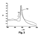
以下、図2及び図3を参照して、中赤外線範囲(3〜5μm)の放射を吸収するための第一の実施形態に係る検出器の性能について説明する。 Hereinafter, the performance of the detector according to the first embodiment for absorbing radiation in the mid-infrared range (3 to 5 μm) will be described with reference to FIGS. 2 and 3.
本実施形態では、基板12はCdZnTe製であり、半導体吸収層14は、中赤外線の吸収用にCdHgTe製である。層14のMCTのCd組成指数は0.3に等しくて、波長λが3から5μm悪くても4μmの間にあるようにする。半導体層14の厚さは、λ/(3×Im(n1))以下であり、この例では300ナノメートルの厚さである。
In this embodiment, the
周期格子18及びミラー22が形成される層16は、ZnSによって構成されて、Au製の周期格子18は、MCT層14から50ナノメートルの距離d、つまり略λ/(40×Re(n1))の距離dに配置される。一方、ミラー22もAu製であり、周期格子18から500ナノメートルの距離h、つまり略λ/(4×Re(n2))の距離hに配置される。
The
更に、周期格子18のピッチpは1.45μm、つまり略1.25×λ/n1の値であり、金属バー20の幅lは500ナノメートルに等しくて、格子18のフィルファクタfが34%に等しくなる。
Further, the pitch p of the
最後に、動作時に、検出器は77Kの温度に冷却される。 Finally, in operation, the detector is cooled to a temperature of 77K.
図2は、あらゆる光生成電荷キャリアが収集されると仮定して、3〜5μmの波長範囲内における、この検出器の吸収応答(曲線“A”)、反射応答(曲線“R”)、及び透過応答(曲線“T”)を示す。図3は、TM偏光及びTE偏光に対する同じ範囲内での量子効率を示す。 FIG. 2 shows the absorption response (curve “A”), reflection response (curve “R”), and reflection response (curve “R”) of this detector within the 3-5 μm wavelength range, assuming that all photogenerated charge carriers are collected. The transmission response (curve “T”) is shown. FIG. 3 shows the quantum efficiency within the same range for TM and TE polarization.
気付かれるように、本発明の検出器は、入射放射の偏光がどうであろうと、80%以上の最大量子効率を有する。残りのうち10%は、構造の金属素子によって吸収され、最後の10%は反射される。 As will be noted, the detector of the present invention has a maximum quantum efficiency of 80% or higher, whatever the polarization of the incident radiation. The remaining 10% is absorbed by the metal element of the structure and the last 10% is reflected.
従来技術の場合のように、格子及びミラーを単純な平面金属ミラーに置換すると、そのミラーからアクティブ層14の距離がどうであろうと、その結果はわずか30%の量子効率になることに留意されたい。
It is noted that replacing the grating and mirror with a simple planar metal mirror, as in the prior art, results in a quantum efficiency of only 30% whatever the distance of the
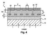
平面金属ミラー22に適合した検出器について説明してきた。代替例として、図4に示されるように、平面金属ミラー22が、例えば周期格子18のパターンと相補的なパターンを有するテクスチャ化金属ミラー32に置換される。例えば、金属バー22は、ミラー32に設けられた同じ表面の凹部に向き合う。
A detector adapted to the
代替例として、図5に示されるように、平面金属ミラー22が、例えば三つの二重層44、46、48で形成されたブラッグミラー42に置換されて、三つの二重層44、46、48の各々は、厚さλ/(4×Re(nGe))のゲルマニウム層と、厚さλ/(4×Re(nZnS))のZnS層によって構成されて、ここで、nGe、nZnSはそれぞれ、ゲルマニウムの屈折率と、硫化亜鉛の屈折率である。
As an alternative, as shown in FIG. 5, the
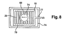
図6は、本発明に係る検出器60の概略的な平面図である。図7及び図8は、それぞれA‐A軸、B‐B軸に沿ったその検出器の概略的な断面図である。検出器60は収集ダイオード62を備える。収集ダイオード62は、PN接合を形成するように例えばp型ドープの吸収層14の導電性と逆の導電性の例えばn型ドープの半導体領域64と、例えば切頭円錐型のメタライゼーション66を備え、そのメタライゼーション66は、層16を貫通して、光電荷キャリアの収集用に半導体領域64に接触している。
FIG. 6 is a schematic plan view of a
後方ミラー68は、上述の理由のために好ましくはテクスチャ化されて、例えば波形となり、メタライゼーション66用の開口70を備えて、ミラー68とメタライゼーション66との間の短絡を防止する。同様に、周期格子18も、メタライゼーション66用の開口74を備えて、その間の短絡を防止する。
The
有利には、メタライゼーション66はミラー68と同じ金属で設けられて、これは、これら二つの素子が同時に製造可能であることを意味する。
Advantageously, the
更に、メタライゼーション66、ミラー68、周期格子18、半導体層14は、それぞれコンタクト75、76、77、78を含んで、異なる電位にすることができて、特に、メタライゼーション66に対して第一の電位V1、ミラー68に対して第二の電位V2、格子18に対して第三の電位V3、半導体層14に対して接地電位に等しい第四の電位Vmである。図8に示されるように、周期格子18のパターンは互いに電気的に接続されて、同じ電位V3になるようにされている。例えば、そのパターンが上述のような平行金属バー20の場合、バー20は、コンタクト77を備えた金属フレーム79内に含まれる。
Furthermore, the
光電荷キャリアは、以下のように収集ダイオード62を介して収集される。
Photocharge carriers are collected through the
コンタクト75と78の間に印加される電位差は、半導体層14と半導体領域64の間のコンタクトによって形成された空間電荷領域における電位降下を誘起する。従って、収集ダイオード62は、僅かな逆電圧バイアスを有する。大抵は周期格子18の下で生成される光電荷キャリアは、空間電荷領域まで拡散して、メタライゼーション66を用いて収集される。
The potential difference applied between the
更に、金属ミラー68、絶縁層16及び半導体層14を組み合わせて、また、金属格子18、絶縁層16及び半導体層16を組み合わせることによって、二つの金属‐絶縁体‐半導体キャパシタが形成される。従って、コンタクト76と78の間に印加される電位差と、コンタクト77と78の間に印加される電位差とは、各々で又は組み合わさって、半導体層14に生成された光電荷キャリアの分布を電界効果で変調させて、ノイズを低減し、電荷収集の効率を高める。
Further, two metal-insulator-semiconductor capacitors are formed by combining the
例えばp型ドープ半導体層14の場合、コンタクト76と78の間及び/又はコンタクト77と78の間に上述の金属‐絶縁体‐半導体スタックのフラットバンド電圧とは異なる電位差を印加することによって、局在化した空乏層を、半導体層14内において、その半導体層14と層16との間の界面の真下に形成することができる。従って、この空乏領域は、光電荷キャリアに対してその界面をマスキングすることによって、半導体層14の中心よりもこの点においてより多くの電気不良があることに鑑み、その界面下における局所的な電子正孔再結合の可能性を低下させる。
For example, in the case of the p-type doped
検出器60の好ましい電気分極構成は複数存在する:
1)ミラー68、格子18及びメタライゼーション66が短絡している、つまり電気的に接続されている構成:これら三つの素子の電位V1=V2=V3は、光電荷キャリアの収集に関するCdHgTe検出器の従来技術の動作に従って、収集ダイオード62のバイアス電圧V1−Vmを決める機能を果たす;
2)ミラー68及び格子18が短絡していてメタライゼーション66から電気的に絶縁されている構成:ミラー68及び格子18の電位V2=V3は、静電ガードとして機能して、半導体層14の上部界面の電気マスキング効果の上述の利点を有し、収集ダイオード62のバイアスはV1−Vmである;
3)ミラー68、格子18及び半導体層14が例えば接地に短絡されていて、ミラー68及び格子18がメタライゼーション66から電気的に絶縁されている構成:これら三つの素子は同じ電位V2=V3=Vmとされて、収集ダイオード62は、電気収集に関するCdHgTe検出器の従来技術の動作に従って、電圧バイアスV1−Vmを有する。このような構成の利点は、半導体層と金属部分18、68の間の近傍に発生する寄生キャパシタンスの制限である。
There are several preferred electrical polarization configurations for detector 60:
1) Configuration in which the
2) Configuration in which the
3) Configuration in which the
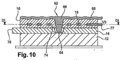
図9は、本発明の一代替例に係る検出器90の概略的な平面図である。図10及び図11は、それぞれC‐C軸、D‐D軸に沿ったその検出器の概略的な断面図である。
FIG. 9 is a schematic plan view of a
検出器90は、メタライゼーション66及びミラー68が単一の構成要素を形成し、アパーチャ70が存在しない点において、上述の検出器60と異なる。従って、メタライゼーション66及びミラー68は、コンタクト75によって同じ電位V1にされて、コンタクト76が省略される。
従って、半導体層14を介する非吸収光子の漏れが防止されて、吸収の量子効率を増強する機能を果たす。実際、上記検出器60においては、メタライゼーション66とミラー68との間のギャップは、例えばリソグラフィ法によって検出器を作製するのに用いられる技術的プロセスの横方向解像度以上でなければならない。このギャップは、低コストUVリソグラフィ技術にとって、例えば1マイクロメートルであり、僅かなものでなくなり得る。検出器90のこの構成は、開口70が存在しないので実施がより単純であるという追加の利点を有する。アパーチャ70によって可能とされるコンタクト75に対してコンタクト76に異なる電位を印加することを可能にする検出器60の構成の利点は、コンタクト76によって印加される電位が、検出器90の構成とは異なり、コンタクト77を介して格子によって印加される電位よりもより空間的に均一なものであることである。
Accordingly, leakage of non-absorbing photons through the
光電荷キャリアは、検出器60に関して上述したのと同様に、検出器90の収集ダイオード62を介して収集されるが、ミラー68を介する独立的なゲート電圧を印加することができない点が異なり、光生成電荷の分布は、格子18に印加される電位のみによって決められる。検出器60と同様に、以下の構成が検出器90に適用可能である:
1)格子18及びメタライゼーション(従ってミラー68も)が短絡している構成:これら三つの素子の電位V1=V2=V3は、光電荷キャリアの収集に関するCdHgTe検出器の従来技術の動作に従って、収集ダイオード62のバイアス電圧V1−Vmを定める機能を果たす;
2)格子18及びメタライゼーション66が絶縁されている構成:格子18の電位V3は静電ガードとして機能して、半導体層14の上部界面の電気マスキング効果の上述の利点を有し、収集ダイオード62のバイアスはV1−Vmである;
3)格子18及び半導体層14が例えば接地に短絡されて、格子18がメタライゼーション66から電気的に絶縁されている構成:これら二つの素子は同じ電位V3=Vmにされて、収集ダイオード62は、電気収集に関するCdHgTe検出器の従来技術の動作に従って、V1−Vmにバイアスされる。このような構成の利点は、半導体層14と金属部分18、68との間の近傍に発生する寄生キャパシタンスの制限である。このキャパシタンスの制限は、検出器60の構成のよりも小さい。何故ならば、寄生キャパシタンスは、格子18とミラー68との間に存在するからである。しかしながら、格子18とミラー68との間の厚さを格子18と半導体層14との間の厚さの略10倍大きくなるように構造の寸法決めをすると、このキャパシタンスは上記1)の構成のものよりも小さくなる。
Photocharge carriers are collected through the
1) Configuration in which the
Configuration 2) grating 18 and the
3) Configuration in which the
半導体層14に生じた光電荷キャリアを収集するために収集ダイオードが設けられた実施形態について説明してきた。
Embodiments have been described in which collection diodes are provided to collect the photocharge carriers generated in the
収集ダイオード62が設けられない代替例では、又は、収集ダイオード62に対する相補的な方法では、周期格子18が、半導体吸収層と接触する(d=0)ように形成されることによって、収集電極として用いられる。この構成の利点は、検出器の速度の上昇である。何故ならば、光電荷キャリアが、収集される前に長距離にわたって拡散する必要がないからである。実際、半導体吸収層14のあらゆる点が、格子18の金属パターンのうちの一つの近くにあることによって、光電荷キャリアが生成される箇所とそれが収集される箇所との間の距離が最小化される。
In an alternative in which the
周期格子が一次元である検出器について説明してきた。このような格子は、入射放射の偏光がどのようなものであれ、量子効率を増強する。しかしながら、図3に示されるように、スペクトル応答は、各偏光に対して厳密に同一ではない。偏光に敏感ではない検出器を作製するためには、又は、各偏光の応答に対する独立的な制御を得るためには、周期格子が二次元であることが有利であり、二つの直交方向に周期性を有する。例えば、周期格子18が、層16内に形成された正方形又は円形の金属パッドの形状の正方形メッシュ格子に置換されて、又は、層16内に配置されて、正方形メッシュ内の正方形又は円形開口でドリル加工された薄い金属膜に置換される。
A detector having a one-dimensional periodic grating has been described. Such a grating enhances quantum efficiency whatever the polarization of the incident radiation. However, as shown in FIG. 3, the spectral response is not exactly the same for each polarization. In order to make a detector that is not sensitive to polarization, or to obtain independent control over the response of each polarization, it is advantageous that the periodic grating is two-dimensional and periodic in two orthogonal directions. Have sex. For example, the
金属パッドの二重周期格子の場合、パッドの電位は浮遊である。図6、図7及び図8で説明された電位構成のおかげで、収集ダイオード62を介する収集に用いられる電位差と、半導体層14内の光生成電荷の分布を修正するのに用いられる電位差とを独立的に制御することができる。
In the case of a double periodic grating of metal pads, the pad potential is floating. Thanks to the potential configuration described in FIGS. 6, 7, and 8, the potential difference used for collection through the
対照的に、金属開口の二重周期格子の場合には、金属格子18の電気的連続性が存在し、図6から図11で説明される手順が適用可能である。 In contrast, in the case of a double periodic grating with a metal opening, there is electrical continuity of the metal grating 18 and the procedure described in FIGS. 6 to 11 is applicable.
こうした二次元周期格子に関する寸法及び距離は、構造の幅以外については、ラインのネットワークの格子18のものと同じである。幅に関しては、p/4≦l≦pとなり、幅lは、正方形の薄いパッドの格子の場合にはパッドの幅であり、薄い金属膜の孔の格子の場合には二つの孔の間の金属空間の幅である。 The dimensions and distances for these two-dimensional periodic gratings are the same as those of the line network grating 18 except for the width of the structure. With regard to the width, p / 4 ≦ l ≦ p, where the width l is the pad width in the case of a square thin pad grid, and between the two holes in the case of a thin metal film hole grid. The width of the metal space.
以下、本発明の検出器(例えば図4のもの)の製造方法を、図12Aから図12Gを参照して説明する。 Hereinafter, a method for manufacturing the detector of the present invention (for example, the one shown in FIG. 4) will be described with reference to FIGS. 12A to 12G.
本製造方法は、基板12(例えばCdZeTe製)上に、対象入射放射を吸収する半導体層(例えば、厚さ300ナノメートルのMCT層等)を成長させることで始まる(図12A)。 The manufacturing method begins by growing a semiconductor layer (eg, a 300 nm thick MCT layer, etc.) that absorbs target incident radiation on a substrate 12 (eg, made of CdZeTe) (FIG. 12A).
そして、本方法は、保護層80(例えば厚さ50ナノメートルのZnS製)を堆積させることに続く(図12B)。そして、電子又は光学樹脂層を、保護層80の上に堆積させて、電子又は紫外線リソグラフィを行って、数百ナノメートル(例えば500ナノメートル)の厚さでパターン82を分離する(図12C)。
The method then continues by depositing a protective layer 80 (eg, 50 nanometer thick ZnS) (FIG. 12B). Then, an electronic or optical resin layer is deposited on the
樹脂を現像した後に、金属84(例えばAu)の“リフトオフ”ステップを行って、周期格子を形成する(図12D)。更に、金属84の厚さは、薄く(例えば50ナノメートル)選択されて、この“リフトオフ”ステップの成功を大幅に促進する。これは、特に、“キャップ”型の欠陥の形成が防止されることを意味する。
After developing the resin, a “lift-off” step of metal 84 (eg, Au) is performed to form a periodic grating (FIG. 12D). In addition, the thickness of the
そして、パターン82をコーティングする金属84を残留樹脂82と共に、例えばアセトン等の溶剤で除去して、周期格子18のみを残す(図12E)。
Then, the
そして、本方法は、半導体吸収層14の屈折率よりも低い屈折率を有する物質86を用いて、厚さhにわたって周期格子18を封止することに続き、格子とミラーとの間に適切な間隔を与える。
The method then encapsulates the
この物質は、例えば厚さ500ナノメートルのZnSであり得る。しかしながら、他の物質も使用可能である。そして、パターン88が、例えばカソードスパッタリングによって、周期格子18のパターン20の上方に形成される(図12F)。
This material can be, for example, ZnS with a thickness of 500 nanometers. However, other materials can be used. Then, the
例えば厚さ10nmのTi下塗り層、続いて厚さ150nmのAu層を堆積させることによって、ミラー32を堆積させる。金は、この最後の層を通る光の透過を防止するのに十分な厚さのものである(図12G)。
For example, the
従って、ミラー32が、周期格子18と同じ周期で構造化されて、その反復パターンの形状は、層の特性、及び周期格子18上に層を堆積させる方法に依存する。特に、ミラー32のテクスチャ化パターンの厚さeは、周期格子18の厚さ以下であって、0とλ/(10×Re(n2))の間であり、例えば、100nmの厚さの周期格子18に対して略100nmである。
Thus, the
図2及び図3を参照して、高い量子効率を優先する実施形態について説明してきた。応用によっては、吸収ピークの幅が不十分であると考えられ得る。 With reference to FIGS. 2 and 3, embodiments have been described that prioritize high quantum efficiency. Depending on the application, the width of the absorption peak may be considered insufficient.
代替実施形態として、半導体層14と格子18との間の距離dを減少させて、このピークの幅を増大させることができる。
As an alternative embodiment, the distance d between the
図13は、厚さ400nmのMCT半導体層14と、1.45μmのピッチp、500nmの幅l、50nmの厚さを有し、500nmの距離hによってミラー22から離隔されている一次元周期格子18に対する距離dの多様な値の関数として、吸収応答を示す。
FIG. 13 shows an
この実施形態例では、距離dは、10nm(最も広いピーク)から300nm(最も狭いピーク)まで変化する。気付かれるように、dが増大すると、吸収ピークの幅が増大する。 In this example embodiment, the distance d varies from 10 nm (widest peak) to 300 nm (narrowest peak). As can be noticed, as d increases, the width of the absorption peak increases.
代替例として、又は相補的な方法において、半導体層14の厚さtを変化させることによっても吸収ピークの幅を制御することができるが、背景強度、つまり共鳴ピークの外側の吸収レベルの上昇を伴う。
As an alternative or in a complementary manner, the width of the absorption peak can also be controlled by changing the thickness t of the
図14は、1.45μmのピッチp、500nmの幅l、50nmの厚さを有し、500nmの距離hによってミラー22から離隔され、50nmの距離dによって層14から離隔された一次元周期格子18について、半導体層14の厚さtの多様な値の関数として、吸収応答を示す。
FIG. 14 shows a one-dimensional periodic grating with a pitch p of 1.45 μm, a width l of 500 nm, a thickness of 50 nm, separated from the
この実施形態例では、層14の厚さtは100nm(左側のピーク、非常に低い)から1000nm(右側のピーク)までのものである。
In this example embodiment, the thickness t of
図8及び図9に示される二つの場合において、良好な共鳴効率、具体的には60%以上の吸収が保たれている。 In the two cases shown in FIGS. 8 and 9, good resonance efficiency, specifically, absorption of 60% or more is maintained.
10 裏面照射型検出器
12 基板(空気層)
14 半導体吸収層
16 絶縁層
18 周期格子
20 金属バー
22 ミラー
10 Back-illuminated
14
Claims (23)
前記電磁放射の吸収用の半導体吸収層(14)であって、前記電磁放射に対して少なくとも部分的に透明な媒体の上方に形成されていて、前記電磁放射の少なくとも一部を透過させる厚さを有する半導体吸収層(14)と、
受光した放射を反射するように前記半導体吸収層(14)の上方に配置されたミラー(22、32、42、68)とを含み、
前記ミラー(22、32、42、68)と前記半導体吸収層(14)との間に配置された金属パターン(20)の周期格子(18)を備え、
前記ミラー(22、32、42、68)及び前記周期格子(18)が、前記電磁放射に対して少なくとも透明な物質層(16)であって、前記半導体吸収層(14)の上に形成された物質層(16)の中に含まれていて、
前記ミラー(22、32、42、68)及び前記金属パターンの周期格子(18)が、
Reが、実部を指称し、
dが、前記半導体吸収層(14)と前記周期格子(18)との間の距離であり、
hが、前記ミラー(22、32、42、68)と前記周期格子(18)との間の距離であり、
mが、正又はゼロの整数であり、
λが、前記半導体吸収層(14)が吸収性を示す波長であり、
n1が、前記半導体吸収層(14)の屈折率であり、
n2が、前記周期格子(18)及び前記ミラー(22、32、42,68)が中に形成されている物質層(16)の屈折率であり、
nsubstratが、前記半導体吸収層(14)が上方に形成されている前記媒体(12)の屈折率である、電磁放射の検出用の裏面照射型検出器。 A back-illuminated detector for detecting electromagnetic radiation near a predetermined wavelength,
A semiconductor absorption layer (14) for absorbing said electromagnetic radiation, which is formed above a medium that is at least partially transparent to said electromagnetic radiation and is transparent to transmit at least part of said electromagnetic radiation. A semiconductor absorption layer (14) having:
A mirror (22, 32, 42, 68) disposed above the semiconductor absorption layer (14) to reflect the received radiation,
A periodic grating (18) of a metal pattern (20) disposed between the mirror (22, 32, 42, 68) and the semiconductor absorption layer (14);
The mirror (22, 32, 42, 68) and the periodic grating (18) are a material layer (16) that is at least transparent to the electromagnetic radiation, and is formed on the semiconductor absorption layer (14). Contained in the material layer (16)
The mirror (22, 32, 42, 68) and the periodic grating (18) of the metal pattern are:
Re designates the real part,
d is the distance between the semiconductor absorption layer (14) and the periodic grating (18);
h is the distance between the mirror (22, 32, 42, 68) and the periodic grating (18);
m is a positive or zero integer;
λ is a wavelength at which the semiconductor absorption layer (14) exhibits absorptivity,
n 1 is the refractive index of the semiconductor absorption layer (14);
n 2 is the refractive index of the material layer (16) in which the periodic grating (18) and the mirror (22, 32, 42, 68) are formed;
A back-illuminated detector for detecting electromagnetic radiation, wherein n substrat is the refractive index of the medium (12) on which the semiconductor absorption layer (14) is formed.
pが前記周期格子(18)のピッチである、請求項1に記載の電磁放射の検出用の裏面照射型検出器。 The periodic grating (18) of the metal pattern is
The back-illuminated detector for detecting electromagnetic radiation according to claim 1, wherein p is the pitch of the periodic grating (18).
前記半導体吸収層(14)内に形成された半導体領域(64)であって、前記半導体吸収層(14)の導電性と逆の導電性を有する半導体領域(64)と、
前記半導体吸収層(14)内に生成された光電荷キャリアを収集するために前記半導体領域(64)と接触して配置されたメタライゼーション(66)とを含む、請求項1から15のいずれか一項に記載の電磁放射の検出用の裏面照射型検出器。 A collecting diode (62), the collecting diode (62) comprising:
A semiconductor region (64) formed in the semiconductor absorption layer (14), wherein the semiconductor region (64) has conductivity opposite to that of the semiconductor absorption layer (14);
A metallization (66) disposed in contact with the semiconductor region (64) for collecting photocharge carriers generated in the semiconductor absorption layer (14). A back-illuminated detector for detecting electromagnetic radiation according to one item.
Applications Claiming Priority (2)
| Application Number | Priority Date | Filing Date | Title |
|---|---|---|---|
| FR1150351 | 2011-01-17 | ||
| FR1150351A FR2970599B1 (en) | 2011-01-17 | 2011-01-17 | PHOTODETECTOR OPTIMIZED BY METALLIC TEXTURATION AGENCED IN REAR FACING |
Publications (1)
| Publication Number | Publication Date |
|---|---|
| JP2012151452A true JP2012151452A (en) | 2012-08-09 |
Family
ID=45401006
Family Applications (1)
| Application Number | Title | Priority Date | Filing Date |
|---|---|---|---|
| JP2011276876A Pending JP2012151452A (en) | 2011-01-17 | 2011-12-19 | Photodetector optimized by metal texturing provided on rear surface |
Country Status (4)
| Country | Link |
|---|---|
| US (1) | US8618622B2 (en) |
| EP (1) | EP2477231A3 (en) |
| JP (1) | JP2012151452A (en) |
| FR (1) | FR2970599B1 (en) |
Families Citing this family (11)
| Publication number | Priority date | Publication date | Assignee | Title |
|---|---|---|---|---|
| FR2969388B1 (en) * | 2010-12-17 | 2013-08-23 | Commissariat Energie Atomique | PHOTODETECTION DEVICE |
| FR2985604B1 (en) * | 2012-01-06 | 2014-03-14 | Commissariat Energie Atomique | PHOTODETECTION DEVICE |
| FR2992470B1 (en) * | 2012-06-26 | 2014-08-08 | Commissariat Energie Atomique | PHOTODETECTOR ELEMENT FOR INFRARED LUMINOUS RADIATION AND PHOTODETECTOR COMPRISING SUCH A PHOTODETECTOR ELEMENT |
| FR3009888B1 (en) * | 2013-08-23 | 2015-09-18 | Commissariat Energie Atomique | SPAD PHOTODIODE WITH HIGH QUANTUM EFFICIENCY |
| FR3009889B1 (en) | 2013-08-23 | 2016-12-23 | Commissariat Energie Atomique | QUANTUM HIGH PERFORMANCE PHOTODIODE |
| FR3015113B1 (en) | 2013-12-17 | 2018-06-01 | Centre National De La Recherche Scientifique- Cnrs | LOW NOISE QUANTUM DETECTION ELEMENT AND METHOD FOR MANUFACTURING SUCH PHOTODETECTION ELEMENT |
| US9985058B2 (en) * | 2016-09-28 | 2018-05-29 | Raytheon Company | Dual band ultraviolet (UV) and infrared radiation detector |
| US9929192B1 (en) | 2016-09-28 | 2018-03-27 | Raytheon Company | Ultraviolet (UV) schottky diode detector having single crystal UV radiation detector material bonded directly to a support structure with proper c-axis orientation |
| CN107665930B (en) * | 2017-08-30 | 2023-05-05 | 中国科学院上海技术物理研究所 | Quantum well infrared detector for realizing wavelength expansion function and design method |
| FR3072458B1 (en) * | 2017-10-12 | 2022-04-01 | Commissariat Energie Atomique | INFRARED RADIATION SOURCE |
| CN107731953B (en) * | 2017-10-24 | 2023-10-31 | 江门市奥伦德光电有限公司 | Photoelectric detector and preparation method thereof |
Family Cites Families (5)
| Publication number | Priority date | Publication date | Assignee | Title |
|---|---|---|---|---|
| US6074892A (en) * | 1996-05-07 | 2000-06-13 | Ciena Corporation | Semiconductor hetero-interface photodetector |
| FR2748604B1 (en) * | 1996-05-13 | 1998-08-07 | Commissariat Energie Atomique | PHOTODETECTOR WITH RESONANT OPTICAL STRUCTURE WITH A NETWORK |
| WO2001001494A1 (en) * | 1999-06-25 | 2001-01-04 | California Institute Of Technology | Multi-directional radiation coupling in quantum-well infrared photodetectors |
| US7238960B2 (en) * | 1999-12-24 | 2007-07-03 | Bae Systems Information And Electronic Systems Integration Inc. | QWIP with enhanced optical coupling |
| US20070235072A1 (en) * | 2006-04-10 | 2007-10-11 | Peter Bermel | Solar cell efficiencies through periodicity |
-
2011
- 2011-01-17 FR FR1150351A patent/FR2970599B1/en not_active Expired - Fee Related
- 2011-12-13 US US13/324,315 patent/US8618622B2/en not_active Expired - Fee Related
- 2011-12-15 EP EP11306668.2A patent/EP2477231A3/en not_active Withdrawn
- 2011-12-19 JP JP2011276876A patent/JP2012151452A/en active Pending
Also Published As
| Publication number | Publication date |
|---|---|
| EP2477231A2 (en) | 2012-07-18 |
| FR2970599A1 (en) | 2012-07-20 |
| US20120181645A1 (en) | 2012-07-19 |
| US8618622B2 (en) | 2013-12-31 |
| FR2970599B1 (en) | 2012-12-28 |
| EP2477231A3 (en) | 2017-12-27 |
Similar Documents
| Publication | Publication Date | Title |
|---|---|---|
| JP2012151452A (en) | Photodetector optimized by metal texturing provided on rear surface | |
| US8750653B1 (en) | Infrared nanoantenna apparatus and method for the manufacture thereof | |
| US9472697B2 (en) | Photodetector with surface plasmon resonance | |
| US7928389B1 (en) | Wide bandwidth infrared detector and imager | |
| TWI772652B (en) | Shallow trench textured regions and associated methods | |
| US9536917B2 (en) | Two color detector leveraging resonant cavity enhancement for performance improvement | |
| CN105981179B (en) | Low noise quantum detecting element and the method for making the optical detection device | |
| JP2012514322A (en) | Photodetector with very thin semiconductor region | |
| US10128386B2 (en) | Semiconductor structure comprising an absorbing area placed in a focusing cavity | |
| JP2011133472A (en) | Photodetector with plasmon structure | |
| US8946839B1 (en) | Reduced volume infrared detector | |
| CN111886704A (en) | Light detector | |
| TW201519455A (en) | Optoelectronic device having surface periodic grating structure and manufacturing method thereof | |
| JP4856031B2 (en) | Avalanche photodiode | |
| US8884271B2 (en) | Photodetection device | |
| US20220155150A1 (en) | Infrared absorption and detection enhancement using plasmonics | |
| CN109668627B (en) | Optical detector with Helmholtz resonator | |
| US9224891B2 (en) | Photodetection device | |
| JP7403670B2 (en) | Electromagnetic wave detectors and electromagnetic wave detector arrays | |
| US11282970B1 (en) | Wideband detector structures | |
| EP2382672B1 (en) | Method of making a photodiode and corresponding photodiode and electromagnetic radiation detector | |
| US11251209B1 (en) | Reduced volume dual-band MWIR detector | |
| CN115425146B (en) | Backside illuminated microstructure array wide-spectrum imaging detector and preparation method thereof | |
| KR101089645B1 (en) | Solar cell having cavity resonance structure and manufacturing method thereof | |
| Schmelz et al. | Back-illuminated normal-incidence Ge-on-Si photodetectors |