JP2012144758A - Terminal for electrical conduction - Google Patents
Terminal for electrical conduction Download PDFInfo
- Publication number
- JP2012144758A JP2012144758A JP2011002211A JP2011002211A JP2012144758A JP 2012144758 A JP2012144758 A JP 2012144758A JP 2011002211 A JP2011002211 A JP 2011002211A JP 2011002211 A JP2011002211 A JP 2011002211A JP 2012144758 A JP2012144758 A JP 2012144758A
- Authority
- JP
- Japan
- Prior art keywords
- conductive terminal
- electrical conductivity
- copper
- pure copper
- metal film
- Prior art date
- Legal status (The legal status is an assumption and is not a legal conclusion. Google has not performed a legal analysis and makes no representation as to the accuracy of the status listed.)
- Pending
Links
Images
Landscapes
- Manufacturing Of Electrical Connectors (AREA)
- Other Surface Treatments For Metallic Materials (AREA)
Abstract
【課題】高い硬度かつ良好な電気伝導性を有し、安価に作製できる導電用端子を提供すること。
【解決手段】純銅、貴金属または前記純銅と前記貴金属との合金を含む粉体をガスと共に加速し、表面に固相状態のままで吹き付けて堆積させることによって形成される金属皮膜からなり、接触対象と接触する接触部133aを備えることによって、安価に作製でき、高い硬度かつ良好な電気伝導性を有する導電用端子13aを得ることができる。
【選択図】図2An object of the present invention is to provide a conductive terminal which has high hardness and good electrical conductivity and can be manufactured at low cost.
A metal film formed by accelerating a powder containing pure copper, a noble metal, or an alloy of the pure copper and the noble metal together with a gas, and spraying and depositing the powder in a solid state on a surface, and to be contacted By providing the contact portion 133a that comes into contact with the conductive terminal 13a, it is possible to obtain the conductive terminal 13a that can be manufactured at low cost and has high hardness and good electrical conductivity.
[Selection] Figure 2
Description
本発明は、電極や電線等の部材間を接合する際に用いられる導電用端子に関する。 The present invention relates to a conductive terminal used when joining members such as electrodes and electric wires.
従来、発電所や自動車等の輸送機器の電気系統、家電製品等において、部材間を接合する溶接のうち、電源供給ライン等として配設される金属部材同士を溶接する方法として、スポット溶接法がある。スポット溶接法は、溶接したい2つの金属部材に対して先細な先端形状をなす電極(導電用端子)をあて、この電極に電流を流して発生した熱によって金属を溶かし、金属部材間を接合する。 Conventionally, spot welding is used as a method for welding metal members arranged as power supply lines, etc., among welding for joining members in electrical systems of household electrical appliances such as power plants and automobiles, and home appliances. is there. In the spot welding method, an electrode (conductive terminal) having a tapered tip shape is applied to two metal members to be welded, the metal is melted by the heat generated by passing an electric current through the electrodes, and the metal members are joined together. .
上述したスポット溶接法によって接合した接合部分では、高い接合強度が求められている。このうち、抵抗率の小さい銅からなる金属部材同士の接合強度を向上させる溶接方法が開示されている(例えば、特許文献1を参照)。 High joint strength is required at the joint portion joined by the spot welding method described above. Among these, the welding method which improves the joining strength of the metal members which consist of copper with small resistivity is disclosed (for example, refer patent document 1).
ところで、従来の電極(導電用端子)を形成する材料として、クロム銅や酸化物分散銅(ODC)が用いられている。クロム銅は、ビッカース硬さ(Hv)が130であり、焼鈍された純銅(無酸素銅)の電気伝導度を100としたときの比率(%)が80%の電気伝導度を有する。また、酸化物分散銅は、例えば、ビッカース硬さ(Hv)が150であり、比率(%)が90%の電気伝導度を有する。導電用端子は、接合対象の部材と繰り返し接触させるため、高い硬度と良好な電気伝導性を有する材料を用いて形成されることが好ましい。 By the way, chromium copper or oxide-dispersed copper (ODC) is used as a material for forming a conventional electrode (conductive terminal). Chromium copper has a Vickers hardness (Hv) of 130, and has an electrical conductivity of 80% when the electrical conductivity of annealed pure copper (oxygen-free copper) is 100. The oxide-dispersed copper has, for example, an electrical conductivity of Vickers hardness (Hv) of 150 and a ratio (%) of 90%. The conductive terminal is preferably formed using a material having high hardness and good electrical conductivity in order to repeatedly contact the member to be joined.
しかしながら、クロム銅は、酸化物分散銅に比べて安価であるものの、クロム銅を用いて形成した導電用端子は、酸化物分散銅を用いて作成したものよりも電極としての硬度および電気伝導度が劣っており、耐久性・操作性の観点から高い硬度および良好な電気伝導性を有することが望まれている。また、酸化物分散銅は、高い硬度と良好な電気伝導性を有する一方、高価であるため、これを用いて導電用端子を形成すると、製造にかかるコストが増大してしまう。 However, although chrome copper is cheaper than oxide-dispersed copper, the conductive terminal formed using chrome copper has higher hardness and electrical conductivity as an electrode than those prepared using oxide-dispersed copper. However, it is desired to have high hardness and good electrical conductivity from the viewpoint of durability and operability. In addition, while oxide-dispersed copper has high hardness and good electrical conductivity, it is expensive. Therefore, when a conductive terminal is formed using this oxide, the manufacturing cost increases.
本発明は、上記に鑑みてなされたものであって、高い硬度かつ良好な電気伝導性を有し、安価に作製できる導電用端子を提供することを目的とする。 The present invention has been made in view of the above, and an object of the present invention is to provide a conductive terminal that has high hardness and good electrical conductivity and can be manufactured at low cost.
上述した課題を解決し、目的を達成するために、本発明にかかる導電用端子は、純銅、貴金属または前記純銅と前記貴金属との合金を含む粉体をガスと共に加速し、表面に固相状態のままで吹き付けて堆積させることによって形成される金属皮膜からなり、接触対象と接触する接触部を備えたことを特徴とする。 In order to solve the above-described problems and achieve the object, the conductive terminal according to the present invention accelerates a powder containing pure copper, a noble metal or an alloy of the pure copper and the noble metal together with a gas, and is in a solid state on the surface. It consists of a metal film formed by spraying and depositing as it is, and has a contact portion that comes into contact with a contact object.
また、本発明にかかる導電用端子は、上記の発明において、純銅、貴金属または純銅と貴金属と合金からなる金属を含む粉体をガスと共に加速し、前記先端部の表面に固相状態のままで吹き付けて堆積させることによって形成された金属皮膜からなることを特徴とする。 Further, the conductive terminal according to the present invention is the above-described invention, wherein the powder containing pure copper, noble metal, or a metal containing a metal composed of pure copper and a noble metal and an alloy is accelerated together with a gas, and remains in a solid state on the surface of the tip. It consists of a metal film formed by spraying and depositing.
また、本発明にかかる導電用端子は、上記の発明において、前記金属皮膜は、ビッカース硬さが120〜170であり、純銅の電気伝導度を100としたときの比率(%)が80〜95%の電気伝導度を有することを特徴とする。 In the conductive terminal according to the present invention, in the above invention, the metal film has a Vickers hardness of 120 to 170, and a ratio (%) when the electric conductivity of pure copper is 100 is 80 to 95. % Electrical conductivity.
また、本発明にかかる導電用端子は、上記の発明において、前記貴金属は、金、銀、白金、イリジウム、パラジウムからなる群より選択される少なくとも1種類を含むことを特徴とする。 In the conductive terminal according to the present invention as set forth in the invention described above, the noble metal includes at least one selected from the group consisting of gold, silver, platinum, iridium, and palladium.
本発明にかかる導電用端子は、少なくとも接合対象の部材と接触する部分を、コールドスプレー法による皮膜によって形成するようにしたので、高い硬度かつ良好な電気伝導性を有し、安価に作製できるという効果を奏する。 The conductive terminal according to the present invention is such that at least a portion in contact with a member to be joined is formed by a film by a cold spray method, so that it has high hardness and good electrical conductivity and can be manufactured at low cost. There is an effect.
以下、本発明を実施するための形態を図面と共に詳細に説明する。なお、以下の実施の形態により本発明が限定されるものではない。また、以下の説明において参照する各図は、本発明の内容を理解し得る程度に形状、大きさ、および位置関係を概略的に示してあるに過ぎない。すなわち、本発明は各図で例示された形状、大きさ、および位置関係のみに限定されるものではない。 DESCRIPTION OF EMBODIMENTS Hereinafter, embodiments for carrying out the present invention will be described in detail with reference to the drawings. In addition, this invention is not limited by the following embodiment. The drawings referred to in the following description only schematically show the shape, size, and positional relationship so that the contents of the present invention can be understood. That is, the present invention is not limited only to the shape, size, and positional relationship illustrated in each drawing.
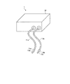
まず、本発明の実施の形態にかかる導電用端子について、図面を参照して詳細に説明する。以下の説明では、導電用端子の例としてスポット溶接装置を説明する。図1は、本実施の形態にかかるスポット溶接装置の構成を模式的に示す斜視図である。図2は、本実施の形態にかかるスポット溶接装置の要部の構成を示す模式図である。図1に示すスポット溶接装置1は、電源供給等を行う本体部10と、本体部10と電気的に接続されるコード11a,11bと、コード11a,11bの本体部10との接続側と異なる端部にそれぞれ電気的に接続される接続部12a,12bと、接続部12a,12bのコード11a,11bとの接続側と異なる端部にそれぞれ電気的に接続され、一対の電極をなす導電用端子13a,13bと、を備える。
First, a conductive terminal according to an embodiment of the present invention will be described in detail with reference to the drawings. In the following description, a spot welding apparatus will be described as an example of the conductive terminal. FIG. 1 is a perspective view schematically showing the configuration of the spot welding apparatus according to the present embodiment. FIG. 2 is a schematic diagram illustrating a configuration of a main part of the spot welding apparatus according to the present embodiment. The spot welding apparatus 1 shown in FIG. 1 is different from the
コード11a,11bは、本体部10と導電用端子13a,13bとが所望の距離となるように延伸されてなる。なお、コード11a,11bの外表面は、絶縁性の樹脂等によって被覆されている。
The
接続部12a,12bは、少なくとも外表面が絶縁性を有する。
At least the outer surfaces of the
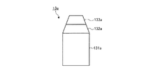
導電用端子13aは、略円柱状をなす基部131aと、基部131aから延びて先細な先端形状をなす先端部132aとを有する(図2参照)。先端部132aは、基部131aの連結側と異なる端部側に、後述するコールドスプレー法によって形成される金属皮膜であって、接合対象部材と接触する接触部133aを有する。導電用端子13a,13bは、接続部12a,12bに対してねじ止めや嵌め合い等によって固定される。基部131aおよび先端部132aは、純銅等の導電性材料を用いて形成される。
The
接触部133aの形成に用いられる金属皮膜(皮膜材料)としては、純銅や、金、銀、白金、イリジウム、パラジウム等の貴金属、または純銅と貴金属との合金が挙げられる。なお、銅よりも電気伝導性に優れる貴金属であれば適用可能である。ここで、金属皮膜は、ビッカース硬さが120〜170であり、純銅の電気伝導度を100としたときの比率(%)が80〜95%の電気伝導度を有することが好ましい。
Examples of the metal film (film material) used for forming the
なお、導電用端子13bについても導電用端子13aと同様に、基部131b、先端部132bおよび接触部133bを有する。
The
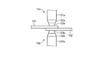
上述した構成を有するスポット溶接装置1は、例えば、図3に示すように、重ね合わせられた状態の接合対象の部材101,102の接触面と反対方向の外表面に対して導電用端子13a,13bの接触部133a,133bをそれぞれ接触させる。本体部10からの電源供給によって、接合対象部材を介して導電用端子13a,13b間が通電する。通電して発生した熱によって接合対象の部材101,102の接触部分を溶かすことで部材101と部材102とを接合する。
For example, as shown in FIG. 3, the spot welding apparatus 1 having the above-described configuration is provided with
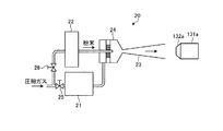
つづいて、接触部133a(金属皮膜)の形成について、図4を参照して説明する。図4は、金属皮膜の形成に使用されるコールドスプレー装置の概要を示す模式図である。コールドスプレー法による金属皮膜形成は、例えば図4に示すコールドスプレー装置20によって行われる。
Next, formation of the
コールドスプレー装置20は、圧縮ガスを加熱するガス加熱器21と、被溶射物に溶射する粉末材料を収容し、スプレーガン24に供給する粉末供給装置22と、スプレーガン24で加熱された圧縮ガスと混合された材料粉末を先端部132aの上面に向けて噴射するガスノズル23とを備えている。
The
圧縮ガスとしては、ヘリウム、窒素、空気などが使用される。供給された圧縮ガスは、バルブ25,26により、ガス加熱器21と粉末供給装置22にそれぞれ供給される。ガス加熱器21に供給された圧縮ガスは、例えば50〜700℃に加熱された後、スプレーガン24に供給される。より好ましくは、先端部132aの上面に噴射される粉末の上限温度を皮膜材料の融点以下に留めるように圧縮ガスを加熱する。粉末材料の加熱温度を皮膜材料の融点以下に留めることにより、皮膜材料の酸化を抑制することができる。
As the compressed gas, helium, nitrogen, air or the like is used. The supplied compressed gas is supplied to the
粉末供給装置22に供給された圧縮ガスは、粉末供給装置22内の、例えば、粒径が10〜100μm程度の材料粉末をスプレーガン24に所定の吐出量となるように供給する。加熱された圧縮ガスは先細末広形状をなすガスノズル23により超音速流(約340m/s以上)に加速される。スプレーガン24に供給された粉末材料は、この圧縮ガスの超音速流の中への投入により加速され、固相状態のまま先端部132aの上面に高速で衝突して皮膜を形成する。
The compressed gas supplied to the
上述したコールドスプレー装置20によって、図2に示すような接触部133aが形成される。なお、材料粉末を先端部132aの上面に固相状態で衝突させて皮膜を形成できるコールドスプレー装置であれば、図4のコールドスプレー装置20に限定されるものではない。
The above-described
上述した処理によって、先端部132aの上面を金属皮膜で覆うことによって接触部133aを形成することができる。皮膜形成後、切削加工等の表面加工処理を施すことによって、表面の形状を調整してもよい。
By the process described above, the
上述した実施の形態にかかるスポット溶接装置の導電用端子によれば、接合対象部材との接触部分をコールドスプレー法によって形成された金属皮膜からなるようにしたので、安価な金属であっても高い硬度の金属皮膜として形成できる。また、コールドスプレー法では、高温で処理する溶接や溶射法等と比して緻密な金属皮膜を形成させることができるため、接触部の電気伝導性が向上する。したがって、一段と良好な電気伝導性を有する導電用端子を実現することができる。 According to the conductive terminal of the spot welding apparatus according to the above-described embodiment, the contact portion with the member to be joined is made of a metal film formed by the cold spray method. It can be formed as a hard metal film. Further, in the cold spray method, a dense metal film can be formed as compared with welding, thermal spraying, or the like that is processed at a high temperature, so that the electrical conductivity of the contact portion is improved. Therefore, a conductive terminal having much better electrical conductivity can be realized.
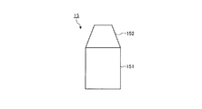
図5は、本実施の形態の変形例にかかるスポット溶接装置の導電用端子の構成を示す模式図である。図5に示す導電用端子15は、略円柱状をなす基部151と、基部151から延びて先細な先端形状をなす先端部152とを有する。基部151および先端部152は、上述したコールドスプレー法によって形成される。このように、導電用端子全体をコールドスプレー法によって作製してもよい。なお、ここで用いられる金属皮膜(皮膜材料)としては、純銅や、金、銀、白金、イリジウム、パラジウム等の貴金属、または純銅と貴金属との合金が挙げられる。
FIG. 5 is a schematic diagram showing a configuration of a conductive terminal of a spot welding apparatus according to a modification of the present embodiment. The conductive terminal 15 shown in FIG. 5 has a
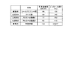
図6は、本発明の実施例にかかる導電用端子に用いる金属皮膜の電気伝導度とビッカース硬さを示す図である。実施例では、コールドスプレー法によって形成された銅の電気伝導度とビッカース硬さを示している。また、比較例1は、クロム銅の電気伝導度とビッカース硬さを示している。比較例2は、酸化物分散銅(アルミナ分散銅1)の電気伝導度とビッカース硬さを示している。比較例3は、酸化物分散銅(アルミナ分散銅2)の電気伝導度とビッカース硬さを示している。なお、実施例および比較例1〜3の電気伝導度は、参考例としての無酸素銅の電気伝導度を100としたときの比率(%)を示している。なお、アルミナ分散銅は数種類存在し、電気伝導度が高いとビッカース硬さは低い。例えば、比較例2のアルミナ分散銅1は、電気伝導度(IACS%)が93%であり、ビッカース硬さ(Hv)が116である。また、比較例3のアルミナ分散銅2は、電気伝導度(IACS%)が77%であり、ビッカース硬さ(Hv)が152である。 FIG. 6 is a diagram showing the electrical conductivity and Vickers hardness of the metal film used for the conductive terminal according to the example of the present invention. In the examples, the electrical conductivity and Vickers hardness of copper formed by the cold spray method are shown. Moreover, the comparative example 1 has shown the electrical conductivity and Vickers hardness of chromium copper. Comparative Example 2 shows the electrical conductivity and Vickers hardness of oxide-dispersed copper (alumina-dispersed copper 1). Comparative Example 3 shows the electrical conductivity and Vickers hardness of oxide-dispersed copper (alumina-dispersed copper 2). In addition, the electrical conductivity of an Example and Comparative Examples 1-3 has shown the ratio (%) when the electrical conductivity of the oxygen-free copper as a reference example is set to 100. FIG. There are several types of alumina-dispersed copper. When the electrical conductivity is high, the Vickers hardness is low. For example, the alumina-dispersed copper 1 of Comparative Example 2 has an electric conductivity (IACS%) of 93% and a Vickers hardness (Hv) of 116. Moreover, the alumina-dispersed copper 2 of Comparative Example 3 has an electric conductivity (IACS%) of 77% and a Vickers hardness (Hv) of 152.
図6に示すように、コールドスプレー法によって形成された銅は、クロム銅よりも電気伝導度(IACS%)およびビッカース硬さが高い値となっている。また、アルミナ分散銅1,2と比較しても、同等の電気伝導度と高いビッカース硬さを示している。ここで、コールドスプレー法で用いた銅は、アルミナ分散銅よりも安価であるため、コールドスプレー法によって銅皮膜を形成して作製した導電用端子は、アルミナ分散銅より安価に、かつ同等以上の電気伝導度およびビッカース硬さを有することが確認できる。 As shown in FIG. 6, the copper formed by the cold spray method has higher electrical conductivity (IACS%) and Vickers hardness than chromium copper. Moreover, even if compared with the alumina-dispersed copper 1 and 2, the same electrical conductivity and high Vickers hardness are shown. Here, since the copper used in the cold spray method is cheaper than the alumina-dispersed copper, the conductive terminal produced by forming a copper film by the cold spray method is cheaper than the alumina-dispersed copper and equal to or more than It can be confirmed that it has electrical conductivity and Vickers hardness.
以上のように、本発明にかかる導電用端子は、高い硬度と良好な電気伝導性を有する接触部を安価に作製することに有用である。 As described above, the conductive terminal according to the present invention is useful for inexpensively producing a contact portion having high hardness and good electrical conductivity.
1 スポット溶接装置
11a,11b コード
12a,12b 接続部
13a,13b,15 導電用端子
131a,131b,151 基部
132a,132b,152 先端部
133a,133b 接触部
20 コールドスプレー装置
21 ガス加熱器
22 粉末供給装置
23 ガスノズル
24 スプレーガン
25,26 バルブ
DESCRIPTION OF SYMBOLS 1
Claims (4)
Priority Applications (1)
| Application Number | Priority Date | Filing Date | Title |
|---|---|---|---|
| JP2011002211A JP2012144758A (en) | 2011-01-07 | 2011-01-07 | Terminal for electrical conduction |
Applications Claiming Priority (1)
| Application Number | Priority Date | Filing Date | Title |
|---|---|---|---|
| JP2011002211A JP2012144758A (en) | 2011-01-07 | 2011-01-07 | Terminal for electrical conduction |
Publications (1)
| Publication Number | Publication Date |
|---|---|
| JP2012144758A true JP2012144758A (en) | 2012-08-02 |
Family
ID=46788623
Family Applications (1)
| Application Number | Title | Priority Date | Filing Date |
|---|---|---|---|
| JP2011002211A Pending JP2012144758A (en) | 2011-01-07 | 2011-01-07 | Terminal for electrical conduction |
Country Status (1)
| Country | Link |
|---|---|
| JP (1) | JP2012144758A (en) |
Cited By (3)
| Publication number | Priority date | Publication date | Assignee | Title |
|---|---|---|---|---|
| JP2014135203A (en) * | 2013-01-10 | 2014-07-24 | Hitachi Vehicle Energy Ltd | Square secondary battery |
| JP2014135204A (en) * | 2013-01-10 | 2014-07-24 | Hitachi Vehicle Energy Ltd | Battery pack |
| KR20180015749A (en) * | 2015-06-08 | 2018-02-13 | 티이 커넥티버티 저머니 게엠베하 | A method for altering mechanical and / or electrical properties of at least one region of an electrical contact element and an electrical contact element |
Citations (6)
| Publication number | Priority date | Publication date | Assignee | Title |
|---|---|---|---|---|
| JPS4121159Y1 (en) * | 1964-02-18 | 1966-10-17 | ||
| JPS6333948B2 (en) * | 1983-03-24 | 1988-07-07 | Sumitomo Light Metal Ind | |
| JP2005095886A (en) * | 2003-09-02 | 2005-04-14 | Nippon Steel Corp | Nozzle for cold spray, cold spray coating and manufacturing method |
| JP2007197795A (en) * | 2006-01-27 | 2007-08-09 | Toyota Motor Corp | Manufacturing method of electronic member |
| JP2008091466A (en) * | 2006-09-29 | 2008-04-17 | Nippon Chemicon Corp | Capacitor |
| JP2009206443A (en) * | 2008-02-29 | 2009-09-10 | Sinto Brator Co Ltd | Method of manufacturing electronic circuit board and electronic circuit board using the same |
-
2011
- 2011-01-07 JP JP2011002211A patent/JP2012144758A/en active Pending
Patent Citations (6)
| Publication number | Priority date | Publication date | Assignee | Title |
|---|---|---|---|---|
| JPS4121159Y1 (en) * | 1964-02-18 | 1966-10-17 | ||
| JPS6333948B2 (en) * | 1983-03-24 | 1988-07-07 | Sumitomo Light Metal Ind | |
| JP2005095886A (en) * | 2003-09-02 | 2005-04-14 | Nippon Steel Corp | Nozzle for cold spray, cold spray coating and manufacturing method |
| JP2007197795A (en) * | 2006-01-27 | 2007-08-09 | Toyota Motor Corp | Manufacturing method of electronic member |
| JP2008091466A (en) * | 2006-09-29 | 2008-04-17 | Nippon Chemicon Corp | Capacitor |
| JP2009206443A (en) * | 2008-02-29 | 2009-09-10 | Sinto Brator Co Ltd | Method of manufacturing electronic circuit board and electronic circuit board using the same |
Cited By (6)
| Publication number | Priority date | Publication date | Assignee | Title |
|---|---|---|---|---|
| JP2014135203A (en) * | 2013-01-10 | 2014-07-24 | Hitachi Vehicle Energy Ltd | Square secondary battery |
| JP2014135204A (en) * | 2013-01-10 | 2014-07-24 | Hitachi Vehicle Energy Ltd | Battery pack |
| KR20180015749A (en) * | 2015-06-08 | 2018-02-13 | 티이 커넥티버티 저머니 게엠베하 | A method for altering mechanical and / or electrical properties of at least one region of an electrical contact element and an electrical contact element |
| CN107710511A (en) * | 2015-06-08 | 2018-02-16 | 泰连德国有限公司 | Electrical contact element and mechanical and/or electrical property the method for changing its at least one region |
| KR102119089B1 (en) * | 2015-06-08 | 2020-06-04 | 티이 커넥티버티 저머니 게엠베하 | Method for changing the mechanical and/or electrical properties of an electrical contact element and at least one region of the electrical contact element |
| US10777912B2 (en) | 2015-06-08 | 2020-09-15 | Te Connectivity Germany Gmbh | Electrical contact element and method for altering mechanical and/or electrical properties of at least one area of such |
Similar Documents
| Publication | Publication Date | Title |
|---|---|---|
| JP5186528B2 (en) | Conductive member and manufacturing method thereof | |
| JP5484360B2 (en) | Conductive member | |
| CN107743429B (en) | Method of connecting conductors to terminal elements and terminal assemblies produced therefrom | |
| US10892671B2 (en) | Electrically conductive copper components and joining processes therefor | |
| JP2012144758A (en) | Terminal for electrical conduction | |
| CN102677069B (en) | A high-performance copper alloy composite integral contact material and its preparation method | |
| JP2006031980A (en) | Heat-resistant insulated wire and fusing method using it | |
| US3519778A (en) | Method and apparatus for joining electrical conductors | |
| US7355142B2 (en) | Resistance welding electrode, welded copper flex lead, and method for making same | |
| JP2014100019A (en) | Terminal structure of electric wire and connection method between electric wire and terminal | |
| JP2023167594A (en) | Electric wire with terminal | |
| JP2020123725A (en) | Electric terminal | |
| JP2644860B2 (en) | Crimp terminal | |
| KR101571616B1 (en) | Sliding contact and method for the production thereof | |
| KR101029222B1 (en) | Method and method for forming a good contact surface on the cathode support bar | |
| JP3888077B2 (en) | ELECTRODE FOR METAL JOINING, ITS MANUFACTURING METHOD, WELDING EQUIPMENT HAVING METAL JOINING ELECTRODE, AND PRODUCT WELDED BY IT | |
| CN117996484A (en) | Contact element, connection assembly, use of a spray medium and method for producing a contact element | |
| JP2003145274A (en) | Method for manufacturing thermocompression bonded terminal and thermocompression bonded terminal | |
| JPH11179536A (en) | Tip for soldering, and its manufacture | |
| JP2019155431A (en) | Joint structure of metal component | |
| JP2004237349A (en) | Joint structure of shape memory alloy and method for forming joint structure | |
| US11862918B2 (en) | Electric wire joining structure, electric wire joining method, and terminal | |
| JPH04298975A (en) | Wire connecting tool and wire connecting method using this tool | |
| GB2103889A (en) | Making connections to electrical brushes | |
| JP2010162565A (en) | Method for manufacturing electric component, arc welding apparatus, and arc welding method |
Legal Events
| Date | Code | Title | Description |
|---|---|---|---|
| A621 | Written request for application examination |
Free format text: JAPANESE INTERMEDIATE CODE: A621 Effective date: 20130809 |
|
| A977 | Report on retrieval |
Free format text: JAPANESE INTERMEDIATE CODE: A971007 Effective date: 20140312 |
|
| A131 | Notification of reasons for refusal |
Free format text: JAPANESE INTERMEDIATE CODE: A131 Effective date: 20140401 |
|
| A521 | Written amendment |
Free format text: JAPANESE INTERMEDIATE CODE: A523 Effective date: 20140530 |
|
| A02 | Decision of refusal |
Free format text: JAPANESE INTERMEDIATE CODE: A02 Effective date: 20141118 |