JP2012144587A - Method for manufacturing compound semiconductor particle - Google Patents
Method for manufacturing compound semiconductor particle Download PDFInfo
- Publication number
- JP2012144587A JP2012144587A JP2011001910A JP2011001910A JP2012144587A JP 2012144587 A JP2012144587 A JP 2012144587A JP 2011001910 A JP2011001910 A JP 2011001910A JP 2011001910 A JP2011001910 A JP 2011001910A JP 2012144587 A JP2012144587 A JP 2012144587A
- Authority
- JP
- Japan
- Prior art keywords
- solution
- component
- raw material
- compound semiconductor
- inp
- Prior art date
- Legal status (The legal status is an assumption and is not a legal conclusion. Google has not performed a legal analysis and makes no representation as to the accuracy of the status listed.)
- Pending
Links
Images
Classifications
-
- H—ELECTRICITY
- H01—ELECTRIC ELEMENTS
- H01L—SEMICONDUCTOR DEVICES NOT COVERED BY CLASS H10
- H01L21/00—Processes or apparatus adapted for the manufacture or treatment of semiconductor or solid state devices or of parts thereof
- H01L21/02—Manufacture or treatment of semiconductor devices or of parts thereof
- H01L21/02104—Forming layers
- H01L21/02365—Forming inorganic semiconducting materials on a substrate
- H01L21/02612—Formation types
- H01L21/02617—Deposition types
- H01L21/02623—Liquid deposition
- H01L21/02628—Liquid deposition using solutions
-
- H—ELECTRICITY
- H01—ELECTRIC ELEMENTS
- H01L—SEMICONDUCTOR DEVICES NOT COVERED BY CLASS H10
- H01L21/00—Processes or apparatus adapted for the manufacture or treatment of semiconductor or solid state devices or of parts thereof
- H01L21/02—Manufacture or treatment of semiconductor devices or of parts thereof
- H01L21/02104—Forming layers
- H01L21/02365—Forming inorganic semiconducting materials on a substrate
- H01L21/02518—Deposited layers
- H01L21/02521—Materials
- H01L21/02538—Group 13/15 materials
- H01L21/02543—Phosphides
-
- H—ELECTRICITY
- H01—ELECTRIC ELEMENTS
- H01L—SEMICONDUCTOR DEVICES NOT COVERED BY CLASS H10
- H01L21/00—Processes or apparatus adapted for the manufacture or treatment of semiconductor or solid state devices or of parts thereof
- H01L21/02—Manufacture or treatment of semiconductor devices or of parts thereof
- H01L21/02104—Forming layers
- H01L21/02365—Forming inorganic semiconducting materials on a substrate
- H01L21/02518—Deposited layers
- H01L21/02521—Materials
- H01L21/02551—Group 12/16 materials
- H01L21/02557—Sulfides
-
- H—ELECTRICITY
- H01—ELECTRIC ELEMENTS
- H01L—SEMICONDUCTOR DEVICES NOT COVERED BY CLASS H10
- H01L21/00—Processes or apparatus adapted for the manufacture or treatment of semiconductor or solid state devices or of parts thereof
- H01L21/02—Manufacture or treatment of semiconductor devices or of parts thereof
- H01L21/02104—Forming layers
- H01L21/02365—Forming inorganic semiconducting materials on a substrate
- H01L21/02518—Deposited layers
- H01L21/02587—Structure
- H01L21/0259—Microstructure
- H01L21/02601—Nanoparticles
Abstract
Description
本発明は、化合物半導体粒子の製造方法に関し、より詳しくは、InPとZnSとが複合された化合物半導体粒子の製造方法に関する。 The present invention relates to a method for producing compound semiconductor particles, and more particularly to a method for producing compound semiconductor particles in which InP and ZnS are combined.
半導体ナノ粒子は、量子閉じ込め効果によって高効率で発光し、量子サイズ効果により発光波長が粒径に応じて変化することから、光機能性材料として有望視されている。この中でも重金属を含まないInPは、可視光領域で良好な発光特性を示すことから、太陽電池や発光ダイオード等の光電変換デバイス材料として注目されている。 Semiconductor nanoparticles are highly promising as optical functional materials because they emit light with high efficiency due to the quantum confinement effect, and the emission wavelength changes according to the particle size due to the quantum size effect. Among them, InP that does not contain heavy metals shows good light emission characteristics in the visible light region, and thus has attracted attention as a photoelectric conversion device material for solar cells, light emitting diodes, and the like.
しかしながら、InPは励起子閉じ込めエネルギーが小さく、このためInPナノ粒子のみで発光させるのは困難である。すなわち、半導体ナノ粒子は、基底状態にある粒子が励起され、励起状態から基底状態に戻るときに発光するが、III−V族化合物半導体であるInPは励起子閉じ込めエネルギーが約5.5meVと小さく、励起子を閉じ込めるための閉じ込めエネルギーが小さいため、室温では励起状態から熱エネルギーで容易に失活し、このためInPナノ粒子単独では発光させるのが困難である。また、フッ酸を使用してInPの表面を光エッチングすることにより、表面欠陥を低減させて発光させることも可能であるが、発光効率が低い上に、製法上煩雑な処理工程が必要となる。 However, InP has a small exciton confinement energy, which makes it difficult to emit light only from InP nanoparticles. That is, semiconductor nanoparticles emit light when particles in the ground state are excited and return from the excited state to the ground state, but InP, which is a group III-V compound semiconductor, has a small exciton confinement energy of about 5.5 meV. Since the confinement energy for confining excitons is small, it is easily deactivated by thermal energy from the excited state at room temperature, and it is difficult to emit light with InP nanoparticles alone. In addition, photoetching of the surface of InP using hydrofluoric acid can reduce the surface defects and cause light emission. However, the luminous efficiency is low, and a complicated process step is required in the manufacturing method. .
そこで、従来より、InPよりもバンドギャップエネルギーの大きいII−VI族化合物半導体、例えばバンドギャップエネルギーが約3.6eVのZnSでInPを被覆し、InPをコア部、ZnSをシェル部としたコア−シェル構造として表面欠陥の低減と同時に励起子の閉じ込めエネルギーを高め、これにより発光させることが行われている。 Therefore, conventionally, a II-VI group compound semiconductor having a larger band gap energy than InP, for example, a core in which InP is coated with ZnS having a band gap energy of about 3.6 eV, with InP as a core portion and ZnS as a shell portion. As a shell structure, surface defects are reduced and at the same time the confinement energy of excitons is increased, thereby causing light emission.
例えば、非特許文献1には、InP/ZnSコア−シェル構造のナノ粒子を作製し、青色の可視光領域から近赤外領域までをカバーすることのできるコロイダルInPナノ結晶の発光体が報告されている。 For example, Non-Patent Document 1 reports a colloidal InP nanocrystal illuminant capable of producing nanoparticles of InP / ZnS core-shell structure and covering from the blue visible light region to the near infrared region. ing.
この非特許文献1では、InP/ZnSコア−シェル構造のナノ粒子を以下のようにして作製している。 In this non-patent document 1, nanoparticles of InP / ZnS core-shell structure are produced as follows.
まず、P源としてのトリストリメチルシリルホスフィン及びオクチルアミンを非極性溶媒であるオクタデセンに溶解させ、P−アミン混合溶液を作製する。次いで、In源としての酢酸インジウム、界面活性剤としてのミリスチン酸、及びオクタデセンとを所定量ずつ秤量して混合し、この混合物をアルゴン雰囲気下、加熱し、これに前記P−アミン混合溶液を注入し、これによりInPナノ粒子溶液を作製する。 First, tristrimethylsilylphosphine and octylamine as a P source are dissolved in octadecene, which is a nonpolar solvent, to prepare a P-amine mixed solution. Next, indium acetate as an In source, myristic acid as a surfactant, and octadecene are weighed and mixed in predetermined amounts, the mixture is heated in an argon atmosphere, and the P-amine mixed solution is injected into the mixture. Thus, an InP nanoparticle solution is prepared.
次いで、Zn源としてのステアリン酸亜鉛をオクタデセンに溶解させたステアリン酸亜鉛溶液、及びイオウ単体をオクタデセンに溶解させたイオウ溶液を用意し、これらステアリン酸亜鉛溶液及びイオウ溶液を所定のヒートサイクルでもって前記InPナノ粒子溶液に注入しInP/ZnSコア−シェル構造のナノ粒子を作製している。具体的には、150℃の温度に調整されたInPナノ粒子溶液にステアリン酸亜鉛溶液及びイオウ溶液を注入し、10分間放置した後、その後温度を220℃まで上昇させて30分間ZnSシェルを成長させ、その後再び150℃に溶液温度を低下させ、以降は上述した一連の処理を繰り返している。そして、所望のInP/ZnSが得られるまで前記一連の処理を複数回繰り返した後、反応溶液を室温まで低下させ、その後ヘキサン、メタノールを用いてメタノール相が透明になるまで抽出精製を行い、未反応物や副生成物を除去した後、クロロホルムやトルエンのような有機溶媒中に分散させ、これによりコア−シェル構造のInP/ZnSナノ粒子分散溶液を得ている。 Next, a zinc stearate solution in which zinc stearate as a Zn source is dissolved in octadecene, and a sulfur solution in which sulfur alone is dissolved in octadecene are prepared, and these zinc stearate solution and sulfur solution are subjected to a predetermined heat cycle. It is injected into the InP nanoparticle solution to produce nanoparticles with an InP / ZnS core-shell structure. Specifically, a zinc stearate solution and a sulfur solution were injected into an InP nanoparticle solution adjusted to a temperature of 150 ° C., left for 10 minutes, and then the temperature was raised to 220 ° C. to grow a ZnS shell for 30 minutes. Then, the solution temperature is lowered again to 150 ° C., and the series of processes described above is repeated thereafter. Then, after repeating the series of treatments several times until the desired InP / ZnS is obtained, the reaction solution is lowered to room temperature, and then extracted and purified using hexane and methanol until the methanol phase becomes transparent. After removing the reactants and by-products, they are dispersed in an organic solvent such as chloroform and toluene, thereby obtaining a core-shell InP / ZnS nanoparticle dispersion solution.
しかしながら、非特許文献1に記載された製法では、上述のように一定のヒートサイクルでもって一連の処理を複数回繰り返さなければならず、製造工程が煩雑な上に再現性にも欠け、高品質のInP/ZnSナノ粒子を安定的に得るのが困難である。 However, in the manufacturing method described in Non-Patent Document 1, a series of processes must be repeated a plurality of times with a constant heat cycle as described above, and the manufacturing process is complicated and the reproducibility is lacking. It is difficult to stably obtain InP / ZnS nanoparticles.
しかも、InPナノ粒子溶液の作製時に残存する未反応のIn源、P源が、ZnやSと予期しない反応を起こすおそれがあり、このため合成プロセスを厳密に管理する必要がある。 In addition, the unreacted In source and P source remaining at the time of preparing the InP nanoparticle solution may cause an unexpected reaction with Zn or S. For this reason, it is necessary to strictly control the synthesis process.
本発明はこのような事情に鑑みなされたものであって、極めて簡便な方法で発光特性の良好なInP−ZnSからなる化合物半導体粒子を高効率に製造できる化合物半導体粒子の製造方法を提供することを目的とする。 The present invention has been made in view of such circumstances, and provides a method for producing compound semiconductor particles capable of producing compound semiconductor particles composed of InP-ZnS having good light emission characteristics with a very simple method with high efficiency. With the goal.
本発明者は、上記目的を達成するために鋭意研究を行ったところ、In成分を含有した原料とZn成分を含有した原料とを溶解させて溶液を作製する一方、P成分を含有した原料とS成分を含有した原料とを溶解させた溶液を作製し、両溶液を接触させることにより、非特許文献1のように煩雑な工程を経なくても、良好な発光特性を有するInP−ZnS複合ナノ粒子を容易かつ高効率に得ることができるという知見を得た。 The present inventor conducted intensive research to achieve the above-described object. As a result, the raw material containing the In component and the raw material containing the Zn component were dissolved to produce a solution, while the raw material containing the P component and An InP-ZnS composite having good light emission characteristics can be obtained by preparing a solution in which a raw material containing an S component is dissolved and bringing both solutions into contact with each other, without having to go through complicated steps as in Non-Patent Document 1. We obtained the knowledge that nanoparticles can be obtained easily and with high efficiency.
本発明はこのような知見に基づきなされたものであって、本発明に係る化合物半導体粒子の製造方法は、In成分を含有した第1の原料とZn成分を含有した第2の原料とを溶解させて第1の溶液を作製する一方、P成分を含有した第3の原料とS成分を含有した第4の原料とを溶解させた第2の溶液を作製し、前記第1の溶液と前記第2の溶液とを接触させてInPとZnSとが複合した化合物半導体粒子を製造することを特徴としている。 The present invention has been made on the basis of such knowledge, and the method for producing compound semiconductor particles according to the present invention dissolves a first raw material containing an In component and a second raw material containing a Zn component. While preparing the first solution, a second solution is prepared by dissolving the third raw material containing the P component and the fourth raw material containing the S component, and the first solution and the It is characterized in that compound semiconductor particles in which InP and ZnS are combined are produced by contacting with a second solution.
また、本発明の化合物半導体粒子の製造方法は、前記第1の溶液を所定温度に加熱し、前記第2の溶液を前記加熱された前記第1の溶液に注入することにより前記第1の溶液と前記第2の溶液とを接触させるのが好ましい。 In the method for producing compound semiconductor particles of the present invention, the first solution is heated by heating the first solution to a predetermined temperature and injecting the second solution into the heated first solution. And the second solution are preferably brought into contact with each other.
また、本発明の化合物半導体粒子の製造方法は、前記第1の溶液が、界面活性剤を含有するのが好ましい。 In the method for producing compound semiconductor particles of the present invention, it is preferable that the first solution contains a surfactant.
また、本発明の化合物半導体粒子の製造方法は、前記第3の原料が、トリストリメチルシリルホスフィンであるのが好ましい。 In the method for producing compound semiconductor particles of the present invention, it is preferable that the third raw material is tristrimethylsilylphosphine.
また、本発明の化合物半導体粒子の製造方法は、前記第4の原料が、ビストリメチルシリルスルフィドであるのが好ましい。 In the method for producing compound semiconductor particles of the present invention, the fourth raw material is preferably bistrimethylsilyl sulfide.
また、本発明の化合物半導体粒子の製造方法は、前記第1の原料が、酢酸インジウムであり、前記第2の原料が、酢酸亜鉛であるのが好ましい。 In the method for producing compound semiconductor particles of the present invention, it is preferable that the first raw material is indium acetate and the second raw material is zinc acetate.
また、本発明の化合物半導体粒子の製造方法は、前記In成分と前記Zn成分との混合比率が、モル比で9/1〜1/9であるのが好ましい。 In the method for producing compound semiconductor particles of the present invention, the mixing ratio of the In component and the Zn component is preferably 9/1 to 1/9 in terms of molar ratio.
上記化合物半導体粒子の製造方法によれば、酢酸インジウム等のIn成分を含有した第1の原料と酢酸亜鉛等のZn成分を含有した第2の原料とを溶解させて第1の溶液を作製する一方、トリストリメチルシリルホスフィン等のP成分を含有した第3の原料とビストリメチルシリルスルフィド等のS成分を含有した第4の原料とを溶解させた第2の溶液を作製し、前記第1の溶液と前記第2の溶液とを接触させてInPとZnSとが複合した化合物半導体粒子を製造するので、非特許文献1のような煩雑な一連の繰り返し工程を経る必要はなく、未反応物や副生成物が生じることもなく、極めて簡便な方法で発光特性の良好な化合物半導体粒子を容易に高効率で得ることができる。 According to the method for producing compound semiconductor particles, a first raw material containing an In component such as indium acetate and a second raw material containing a Zn component such as zinc acetate are dissolved to produce a first solution. On the other hand, a second solution in which a third raw material containing a P component such as tristrimethylsilylphosphine and a fourth raw material containing an S component such as bistrimethylsilylsulfide are dissolved is prepared. Since compound semiconductor particles in which InP and ZnS are combined are produced by contacting with the second solution, it is not necessary to go through a complicated series of repeating steps as in Non-Patent Document 1, and unreacted substances and by-products are produced. No compound is produced, and compound semiconductor particles having good light emission characteristics can be easily obtained with high efficiency by an extremely simple method.
具体的には、前記第1の溶液を所定温度に加熱し、前記第2の溶液を前記加熱された前記第1の溶液に注入することにより前記第1の溶液と前記第2の溶液とを接触させることにより、前記第1の溶液と第2の溶液との間で合成反応が容易に進行し、これによりInP−ZnS複合ナノ粒子を高効率で得ることができる。 Specifically, the first solution and the second solution are heated by heating the first solution to a predetermined temperature and injecting the second solution into the heated first solution. By contacting, the synthesis reaction easily proceeds between the first solution and the second solution, whereby InP—ZnS composite nanoparticles can be obtained with high efficiency.
また、前記第1の溶液は、界面活性剤を含有することにより、第1及び第2の溶液が接触後に生成したナノ粒子が凝集するのを回避することができ、分散性の良好なナノ粒子分散液を合成することができる。 In addition, the first solution contains a surfactant, so that the nanoparticles formed after the first and second solutions are brought into contact can be prevented from agglomerating, and the nanoparticles having good dispersibility can be avoided. A dispersion can be synthesized.
また、前記In成分と前記Zn成分との混合比率をモル比で9/1〜1/9とすることにより、可視光領域で発光波長のピークが異なるInP−ZnSからなる種々の化合物半導体ナノ粒子を容易に得ることができる。 Various compound semiconductor nanoparticles composed of InP-ZnS having different emission wavelength peaks in the visible light region by setting the mixing ratio of the In component and the Zn component to 9/1 to 1/9 in terms of molar ratio. Can be easily obtained.
次に、本発明を実施するための形態を詳説する。 Next, the form for implementing this invention is explained in full detail.
本発明に係る化合物半導体粒子の製造方法は、In成分を含有した第1の原料とZn成分を含有した第2の原料とを溶解させて第1の溶液を作製する一方、P成分を含有した第3の原料とS成分を含有した第4の原料とを溶解させた第2の溶液を作製し、第1の溶液と第2の溶液とを接触させるようにしたものであり、これにより第1の溶液と第2の溶液とが反応し、InP−ZnS複合ナノ粒子を作製することができる。 The method for producing a compound semiconductor particle according to the present invention dissolves the first raw material containing the In component and the second raw material containing the Zn component to produce the first solution, while containing the P component. A second solution in which the third raw material and the fourth raw material containing the S component are dissolved is prepared, and the first solution and the second solution are brought into contact with each other. The solution of 1 and the second solution react to produce InP-ZnS composite nanoparticles.
〔背景技術〕の項でも述べたように、重金属を含まないInPのナノ粒子は、太陽電池や発光ダイオード等の光電変換デバイス材料として注目されているが、InPは励起子閉じ込めエネルギーが小さいことから、熱エネルギーで容易に失活してしまうため、InP単独で発光させるのは困難である。 As described in [Background Art], InP nanoparticles that do not contain heavy metals are attracting attention as photoelectric conversion device materials such as solar cells and light-emitting diodes, but InP has a low exciton confinement energy. Since it is easily deactivated by thermal energy, it is difficult to emit light with InP alone.
このため、従来では、InPよりもバンドギャップエネルギーの大きなZnSで前記InPを被覆し、InPをコア部、ZnSをシェル部としたコア−シェル構造とすることにより、励起子の閉じ込めエネルギーを高め、これにより所望の発光させていた。 For this reason, conventionally, the InP is coated with ZnS having a larger band gap energy than InP, and a core-shell structure in which InP is a core portion and ZnS is a shell portion, thereby increasing the exciton confinement energy, As a result, the desired light was emitted.
そして、斯かるコア−シェル構造のInP/ZnSでは、InPナノ粒子の表面をZnSで被覆させる必要があることから、非特許文献1に記載されているように、InPナノ粒子溶液を作製し、その後、このInPナノ粒子溶液に亜鉛含有溶液及びイオウ含有溶液を注入して合成していた。 And in InP / ZnS of such a core-shell structure, since it is necessary to coat the surface of InP nanoparticles with ZnS, an InP nanoparticle solution is prepared as described in Non-Patent Document 1, Thereafter, a zinc-containing solution and a sulfur-containing solution were injected into the InP nanoparticle solution and synthesized.
しかしながら、〔発明が解決しようとする課題〕の項でも述べたように、上述のような製造方法では、ヒートサイクルを含む一連の繰り返し工程を経なければならず、製造工程が煩雑な上に高品質の化合物半導体粒子を得るのが困難であり、コスト面も含め生産性に劣っていた。 However, as described in the section of [Problems to be Solved by the Invention], in the manufacturing method as described above, a series of repeating steps including a heat cycle must be performed, which makes the manufacturing process complicated and expensive. It was difficult to obtain quality compound semiconductor particles, and the productivity was inferior including the cost.
そこで、本発明者が鋭意研究を行ったところ、上記製法に代わる新たな製法としてIn成分及びZn成分を含有した溶液にP成分及びS成分を含有した溶液を注入し、両溶液を接触させることにより、極めて簡便な方法で発光特性の良好なInP−ZnSの複合ナノ粒子を合成できることを見出した。そして、これにより従来のようにヒートサイクルを含む一連の繰り返し工程を経る必要もなく、また、未反応物質が残存したり副生成物が製造されることもなく、高効率で高品質なInP−ZnSからなる化合物半導体ナノ粒子を得ることができる。 Then, when the present inventor conducted earnest research, as a new production method replacing the above production method, a solution containing P component and S component was injected into a solution containing In component and Zn component, and both solutions were brought into contact with each other. Thus, it was found that InP—ZnS composite nanoparticles having excellent light emission characteristics can be synthesized by an extremely simple method. As a result, it is not necessary to go through a series of repeated steps including a heat cycle as in the prior art, and no unreacted substances remain or by-products are produced. Compound semiconductor nanoparticles made of ZnS can be obtained.
尚、本発明では化合物半導体ナノ粒子の形態は、特に限定されるものではなく、InP/ZnSコア−シェル構造、InPとZnSとの複合体、或いは前記コア−シェル構造と前記複合体との混合物のいずれであってもよく、いずれの場合も所望の良好な発光特性を得ることができる。例えば、前記コア−シェル構造の場合は、InPはZnSによって閉じ込め効果が高められて励起子発光し、また、前記複合体の場合は、励起子閉じ込めエネルギーの高いZnSとの複合化により、発光するに十分な閉じ込めエネルギーを得ることができ、いずれの場合も良好な発光特性を得ることができる。 In the present invention, the form of the compound semiconductor nanoparticles is not particularly limited, and is an InP / ZnS core-shell structure, a composite of InP and ZnS, or a mixture of the core-shell structure and the composite. In any case, desired good light emission characteristics can be obtained. For example, in the case of the core-shell structure, InP emits excitons by enhancing the confinement effect by ZnS, and in the case of the complex, it emits light by complexing with ZnS having high exciton confinement energy. Sufficient confinement energy can be obtained, and in any case, good light emission characteristics can be obtained.
以下、上記化合物半導体粒子の製造方法の一例を具体的に詳述する。 Hereinafter, an example of the manufacturing method of the said compound semiconductor particle is explained in full detail.
まず、In成分を含有した第1の原料、Zn成分を含有した第2の原料、界面活性剤、及びこれらに溶解する有機溶媒を用意する。そしてこれらを所定量秤量して混合し、真空脱気させた後、必要に応じて窒素雰囲気下、加熱し、これにより第1の原料及び第2の原料を有機溶媒に溶解させ、第1の溶液を作製する。 First, a first raw material containing an In component, a second raw material containing a Zn component, a surfactant, and an organic solvent dissolved therein are prepared. These are weighed and mixed in a predetermined amount, vacuum degassed, and then heated under a nitrogen atmosphere as necessary, whereby the first raw material and the second raw material are dissolved in an organic solvent, and the first Make a solution.
第1の原料と第2の原料との混合比率は、特に限定されるものではないが、In成分とZn成分とがモル比で1/9〜9/1となるように調整するのが好ましく、斯かる範囲で発光特性の低下を招くことなく、可視光領域での発光波長の波長ピークを調整することが可能である。 The mixing ratio of the first raw material and the second raw material is not particularly limited, but it is preferable to adjust the In component and the Zn component so that the molar ratio is 1/9 to 9/1. In such a range, it is possible to adjust the wavelength peak of the emission wavelength in the visible light region without causing deterioration of the emission characteristics.
尚、In成分とZn成分の混合比率が1/9未満になると、ナノ粒子中のZnSの含有モル量が過剰となり、このため発光波長が短波長側に変移して可視光領域外となって視認できなくなる。一方、In成分とZn成分の混合比率が9/1を超えると、ナノ粒子中のZnSの含有モル量が少なくなってバンドギャップエネルギーが赤外域となり視認できなくなる。 When the mixing ratio of the In component and the Zn component is less than 1/9, the content molar amount of ZnS in the nanoparticles becomes excessive, so that the emission wavelength shifts to the short wavelength side and becomes out of the visible light region. It becomes invisible. On the other hand, when the mixing ratio of the In component and the Zn component exceeds 9/1, the content molar amount of ZnS in the nanoparticles decreases, and the band gap energy becomes in the infrared region and cannot be visually recognized.
また、第1の原料としては、In成分を含有していれば特に限定されるものではなく、例えば、酢酸インジウム、塩化インジウム、ヨウ化インジウム、炭酸インジウム、インジウムアセチルアセトナート、臭化インジウム、フッ化インジウム等を使用することができる。 The first raw material is not particularly limited as long as it contains an In component. For example, indium acetate, indium chloride, indium iodide, indium carbonate, indium acetylacetonate, indium bromide, fluorine Indium chloride or the like can be used.
第2の原料としては、Zn成分を含有していれば特に限定されるものではなく、酢酸亜鉛、塩化亜鉛、ヨウ化亜鉛、臭化亜鉛、フッ化亜鉛、酸化亜鉛、亜鉛アセチルアセトナート等を使用することができる。 The second raw material is not particularly limited as long as it contains a Zn component, and includes zinc acetate, zinc chloride, zinc iodide, zinc bromide, zinc fluoride, zinc oxide, zinc acetylacetonate, and the like. Can be used.
界面活性剤は、第1の原料同士、第2の原料同士、或いは第1の原料と第2の原料が凝集するのを回避するために分散剤として混入され、例えば、ミリスチン酸、ラウリン酸、パルミチン酸、マルガリン酸、ステアリン酸、オレイン酸、パクセン酸、リノール酸、カプリル酸等を使用することができる。 The surfactant is mixed as a dispersant in order to avoid the aggregation of the first raw materials, the second raw materials, or the first raw material and the second raw material. For example, myristic acid, lauric acid, Palmitic acid, margaric acid, stearic acid, oleic acid, paxenoic acid, linoleic acid, caprylic acid and the like can be used.
有機溶媒についても、第1及び第2の原料に溶解するものであれば特に限定するものではなく、例えば、オレイルアミン等の脂肪族アミン、オクタデカン等のアルカンやオクタデセン等のアルケンを使用することができる。 The organic solvent is not particularly limited as long as it is soluble in the first and second raw materials. For example, aliphatic amines such as oleylamine, alkanes such as octadecane, and alkenes such as octadecene can be used. .
次に、P成分を含有した第3の原料、S成分を含有した第4の原料、及び両者に溶解する有機溶媒を用意し、第3及び第4の原料を有機溶媒に溶解させ、第2の溶液を作製する。 Next, a third raw material containing the P component, a fourth raw material containing the S component, and an organic solvent that dissolves in both are prepared, and the third and fourth raw materials are dissolved in the organic solvent, A solution of
第3の原料としては、P成分を含有していれば特に限定されるものではなく、例えば、トリストリメチルシリルホスフィン、トリストリエチルシリルホスフィン等を使用することができるが、これらの中では反応性に富んだトリストリメチルシリルホスフィンを好んで使用することができる。 The third raw material is not particularly limited as long as it contains a P component. For example, tristrimethylsilylphosphine, tristriethylsilylphosphine, and the like can be used. Tristrimethylsilylphosphine can be preferably used.
第4の原料としては、S成分を含有していれば特に限定されるものではなく、イオウ単体やビストリメチルシリルスルフィド、ビストリエチルシリルスルフィド、ビストリプロピルシリルスルフィド等のアルキルシリル化イオウ化合物等を使用することができるが、これらの中では反応性に富んだアルキルシリル化イオウ化合物を好んで使用することができる。 The fourth raw material is not particularly limited as long as it contains an S component, and a sulfur alone or an alkylsilylated sulfur compound such as bistriethylsilyl sulfide, bistriethylsilyl sulfide, or bistripropylsilyl sulfide is used. Of these, highly reactive alkylsilylated sulfur compounds can be preferably used.
また、有機溶媒についても、上述と同様、第3及び第4の原料に溶解するものであれば特に限定するものではなく、例えば、オレイルアミン等の脂肪族アミン、オクタデカン等のアルカンやオクタデセン等のアルケンを使用することができる。 The organic solvent is not particularly limited as long as it is soluble in the third and fourth raw materials as described above. For example, aliphatic amines such as oleylamine, alkanes such as octadecane, and alkenes such as octadecene. Can be used.
次いで、第1の溶液を所定温度に加熱させた状態で第2の溶液を注入し、第1の溶液と第2の溶液とを接触させ、所定時間保持した後、室温まで冷却する。そしてこれにより、平均粒径が2〜5nmのInP−ZnS複合ナノ粒子溶液を作製することができる。 Next, the second solution is injected while the first solution is heated to a predetermined temperature, the first solution and the second solution are brought into contact with each other, held for a predetermined time, and then cooled to room temperature. Thereby, an InP—ZnS composite nanoparticle solution having an average particle diameter of 2 to 5 nm can be produced.
このように本実施の形態では、In成分を含有した第1の原料とZn成分を含有した第2の原料とを溶解させて第1の溶液を作製する一方、P成分を含有した第3の原料とS成分を含有した第4の原料とを溶解させた第2の溶液を作製し、前記第1の溶液と前記第2の溶液とを接触させてInPとZnSとが複合した化合物半導体粒子を製造するので、非特許文献1に記載されたような煩雑な一連の繰り返し工程を経る必要はなく、また未反応物や副生成物が生じることもなく、極めて簡便な方法で発光特性の良好な化合物半導体粒子を高効率で得ることができる。 As described above, in the present embodiment, the first raw material containing the In component and the second raw material containing the Zn component are dissolved to produce the first solution, while the third raw material containing the P component is used. A compound semiconductor particle in which a second solution in which a raw material and a fourth raw material containing an S component are dissolved is prepared and InP and ZnS are combined by bringing the first solution and the second solution into contact with each other Therefore, it is not necessary to go through a complicated series of repeating steps as described in Non-Patent Document 1, and there is no generation of unreacted products and by-products. Compound semiconductor particles can be obtained with high efficiency.
すなわち、前記第1の溶液を所定温度に加熱し、前記第2の溶液を前記加熱された前記第1の溶液に注入することにより前記第1の溶液と前記第2の溶液とを接触させることにより、前記第1の溶液と第2の溶液との間で合成反応が容易に進行し、これによりInP−ZnS複合ナノ粒子を高効率で得ることができる。 That is, contacting the first solution and the second solution by heating the first solution to a predetermined temperature and injecting the second solution into the heated first solution. Thus, the synthesis reaction easily proceeds between the first solution and the second solution, whereby InP—ZnS composite nanoparticles can be obtained with high efficiency.
また、前記第1の溶液に界面活性剤を含有させているので、第1及び第2の溶液の接触後に生成するナノ粒子の分散性を確保することができる。 In addition, since the surfactant is contained in the first solution, it is possible to ensure the dispersibility of the nanoparticles generated after the contact between the first and second solutions.
また、前記In成分と前記Zn成分との混合比率をモル比で9/1〜1/9とすることにより、可視光領域で発光波長のピークが異なるInP−ZnSからなる種々の化合物半導体ナノ粒子を容易に得ることができる。 Various compound semiconductor nanoparticles composed of InP-ZnS having different emission wavelength peaks in the visible light region by setting the mixing ratio of the In component and the Zn component to 9/1 to 1/9 in terms of molar ratio. Can be easily obtained.
尚、本発明は上記実施の形態に限定されるものではなく、要旨を変更しない範囲で種々の変形が可能であるのはいうまでもない。 Needless to say, the present invention is not limited to the above embodiment, and various modifications can be made without departing from the scope of the invention.
次に、本発明の実施例を具体的に説明する。 Next, examples of the present invention will be specifically described.
〔試料番号1〕
第1の原料として酢酸インジウム(In(CH3COO)3)、第2の原料として酢酸亜鉛(Zn(CH3COO)2・2H2O)、界面活性剤としてミリスチン酸(C13H27COOH)、非極性溶媒としてオクタデセン(C18H36)を用意した。そして、In成分とZn成分の混合比率がモル比で1:1となるように、酢酸インジウム及び酢酸亜鉛をそれぞれ0.4ミリモルずつ秤量し、さらにミリスチン酸1.2ミリモル、及びオクタデセン19.6gを秤量した。そしてこれら秤量物をセプタムキャップ付き三つ口フラスコに投入し、100℃の温度で30分間、真空脱気した。次いで、雰囲気を窒素置換し、マントルヒータを使用して三つ口フラスコを300℃の温度に加熱し、これにより三つ口フラスコの内容物を溶解させ、第1の溶液を作製した。
[Sample No. 1]
Indium acetate (In (CH 3 COO) 3 ) as the first raw material, zinc acetate (Zn (CH 3 COO) 2 · 2H 2 O) as the second raw material, and myristic acid (C 13 H 27 COOH as the surfactant) ), Octadecene (C 18 H 36 ) was prepared as a nonpolar solvent. Then, 0.4 mmol each of indium acetate and zinc acetate was weighed so that the mixing ratio of the In component and the Zn component was 1: 1, and 1.2 mmol of myristic acid and 19.6 g of octadecene. Was weighed. These weighed products were put into a three-necked flask with a septum cap and vacuum deaerated at a temperature of 100 ° C. for 30 minutes. Next, the atmosphere was replaced with nitrogen, and the three-necked flask was heated to a temperature of 300 ° C. using a mantle heater, whereby the contents of the three-necked flask were dissolved to prepare a first solution.
次に、第3の原料としてトリストリメチルシリルホスフィン(C9H27PSi3)、第4の原料としてビストリメチルシリルスルフィド(C6H18SSi2)、及びオクタデセンを用意した。そして、これらトリストリメチルシリルホスフィン0.2ミリモル、ビストリメチルシリルスルフィド0.2ミリモル、及びオクタデセン8gをグローブボックス中でバイアル瓶に測り採って溶解させ、第2の溶液を作製した。 Next, tristrimethylsilylphosphine (C 9 H 27 PSi 3 ) was prepared as a third raw material, and bistrimethylsilyl sulfide (C 6 H 18 SSi 2 ) and octadecene were prepared as a fourth raw material. Then, 0.2 mmol of tristrimethylsilylphosphine, 0.2 mmol of bistrimethylsilylsulfide, and 8 g of octadecene were measured and dissolved in a vial in a glove box to prepare a second solution.
次いで、300℃に加熱した第1の溶液中にセプタムキャップの上方から第2の溶液を注射器で一気に注入した後、マントルヒータの温度を270℃に設定して3時間を保持し、その後室温になるまで自然冷却し、これにより試料番号1のInP−ZnS複合ナノ粒子溶液を作製した。尚、InP−ZnS複合ナノ粒子の粒径を透過電子顕微鏡で測定したところ、平均粒径は3nmであった。 Then, after injecting the second solution from above the septum cap into the first solution heated to 300 ° C. with a syringe, the temperature of the mantle heater is set to 270 ° C. and maintained for 3 hours, and then the temperature is brought to room temperature. The InP-ZnS composite nanoparticle solution of Sample No. 1 was produced. In addition, when the particle diameter of the InP-ZnS composite nanoparticles was measured with a transmission electron microscope, the average particle diameter was 3 nm.
〔試料番号2〕
In成分とZn成分の混合比率がモル比で9:1となるように酢酸インジウム0.72ミリモル及び酢酸亜鉛0.08ミリモルを秤量し、またトリストリメチルシリルホスフィン0.36ミリモル、ビストリメチルシリルスルフィド0.04ミリモルを秤量した以外は、試料番号1と同様の方法・手順で試料番号2のInP−ZnS複合ナノ粒子溶液を作製した。尚、試料番号1と同様の方法・手順で、InP−ZnS複合ナノ粒子の粒径を測定したところ、平均粒径は5nmであった。
[Sample No. 2]
0.72 mmol of indium acetate and 0.08 mmol of zinc acetate were weighed so that the mixing ratio of the In component and the Zn component was 9: 1. An InP-ZnS composite nanoparticle solution of Sample No. 2 was prepared in the same manner and procedure as Sample No. 1 except that 04 mmol was weighed. In addition, when the particle diameter of the InP-ZnS composite nanoparticles was measured by the same method and procedure as in Sample No. 1, the average particle diameter was 5 nm.
〔試料番号3〕
In成分とZn成分の混合比率がモル比で1:9となるように、酢酸インジウム0.08ミリモル、酢酸亜鉛を0.72ミリモルを秤量し、またトリストリメチルシリルホスフィン0.04ミリモル、ビストリメチルシリルスルフィド0.36ミリモルを秤量した以外は、試料番号1と同様の方法・手順で試料番号3のInP−ZnS複合ナノ粒子溶液を作製した。尚、試料番号1と同様の方法・手順で、InP−ZnS複合ナノ粒子の粒径を測定したところ、平均粒径は2nmであった。
[Sample No. 3]
0.08 mmol of indium acetate and 0.72 mmol of zinc acetate were weighed so that the mixing ratio of In component and Zn component was 1: 9, and tristrimethylsilylphosphine 0.04 mmol, bistrimethylsilyl sulfide. An InP-ZnS composite nanoparticle solution of Sample No. 3 was prepared in the same manner and procedure as Sample No. 1 except that 0.36 mmol was weighed. In addition, when the particle diameter of the InP-ZnS composite nanoparticles was measured by the same method and procedure as in Sample No. 1, the average particle diameter was 2 nm.
〔試料の評価〕
試料番号1〜3のナノ粒子溶液を少量採取し、トルエンで希釈した後、波長300nmの励起光を用いて発光特性を測定した。
(Sample evaluation)
A small amount of the nanoparticle solutions of sample numbers 1 to 3 were collected and diluted with toluene, and then the emission characteristics were measured using excitation light having a wavelength of 300 nm.
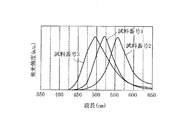
図1は、試料番号1〜3の発光スペクトルを示し、横軸が波長(nm)、縦軸が発光強度(a.u.)である。 FIG. 1 shows the emission spectra of Sample Nos. 1 to 3, where the horizontal axis represents wavelength (nm) and the vertical axis represents emission intensity (a.u.).
この図1から明らかなように、試料番号1では、波長ピークが520nmの光が観察され、試料番号2では、波長ピークが560nmの光が観察され、試料番号3では、波長ピークが490nmの光が観察された。すなわち、In成分とZn成分との混合比率が大きくなると、発光波長の波長ピークが長波長側に変移し、In成分とZn成分との混合比率が小さくなるに伴い、発光波長の波長ピークが短波長側に変移することが分かった。尚、量子効率は、いずれの試料についても4〜8%であった。 As is clear from FIG. 1, light having a wavelength peak of 520 nm is observed in sample number 1, light having a wavelength peak of 560 nm is observed in sample number 2, and light having a wavelength peak of 490 nm is observed in sample number 3. Was observed. That is, when the mixing ratio of the In component and the Zn component increases, the wavelength peak of the emission wavelength shifts to the longer wavelength side, and the wavelength peak of the emission wavelength decreases as the mixing ratio of the In component and the Zn component decreases. It turned out to shift to the wavelength side. The quantum efficiency was 4 to 8% for all samples.
煩雑な繰り返し工程を経なくても、未反応物や副生成物が生じることもなく、極めて簡便な方法で発光特性の良好なInP−ZnS複合ナノ粒子を高効率で得ることができ、太陽電池や発光ダイオード等の光電変換デバイスに利用可能な新規な化合物半導体ナノ粒子の製法を実現できる。 InP-ZnS composite nanoparticles with good light-emitting properties can be obtained with high efficiency by an extremely simple method without going through complicated repeating steps and without generation of unreacted products and by-products. And a novel method for producing compound semiconductor nanoparticles that can be used for photoelectric conversion devices such as light-emitting diodes.
Claims (7)
前記第1の溶液と前記第2の溶液とを接触させてInPとZnSとが複合した化合物半導体粒子を製造することを特徴とする化合物半導体粒子の製造方法。 The first raw material containing the In component and the second raw material containing the Zn component are dissolved to produce the first solution, while the third raw material containing the P component and the fourth containing the S component. A second solution in which the raw material is dissolved,
A method for producing compound semiconductor particles, wherein the first solution and the second solution are brought into contact with each other to produce compound semiconductor particles in which InP and ZnS are combined.
Priority Applications (1)
| Application Number | Priority Date | Filing Date | Title |
|---|---|---|---|
| JP2011001910A JP2012144587A (en) | 2011-01-07 | 2011-01-07 | Method for manufacturing compound semiconductor particle |
Applications Claiming Priority (1)
| Application Number | Priority Date | Filing Date | Title |
|---|---|---|---|
| JP2011001910A JP2012144587A (en) | 2011-01-07 | 2011-01-07 | Method for manufacturing compound semiconductor particle |
Publications (1)
| Publication Number | Publication Date |
|---|---|
| JP2012144587A true JP2012144587A (en) | 2012-08-02 |
Family
ID=46788498
Family Applications (1)
| Application Number | Title | Priority Date | Filing Date |
|---|---|---|---|
| JP2011001910A Pending JP2012144587A (en) | 2011-01-07 | 2011-01-07 | Method for manufacturing compound semiconductor particle |
Country Status (1)
| Country | Link |
|---|---|
| JP (1) | JP2012144587A (en) |
Cited By (4)
| Publication number | Priority date | Publication date | Assignee | Title |
|---|---|---|---|---|
| US20110227007A1 (en) * | 2010-03-22 | 2011-09-22 | Samsung Electronics Co., Ltd. | Method of manufacturing quantum dot |
| WO2016080435A1 (en) * | 2014-11-20 | 2016-05-26 | 富士フイルム株式会社 | Core-shell particles, method for preparing core-shell particles, and film |
| WO2018198684A1 (en) * | 2017-04-25 | 2018-11-01 | 富士フイルム株式会社 | Semiconductor nanoparticles, semiconductor nanoparticle-containing dispersion liquid, and film |
| TWI831967B (en) | 2020-04-30 | 2024-02-11 | 日商日油股份有限公司 | Zinc carboxylate composition and zinc carboxylate solution containing the zinc carboxylate composition |
Citations (2)
| Publication number | Priority date | Publication date | Assignee | Title |
|---|---|---|---|---|
| FR2930786A1 (en) * | 2008-05-05 | 2009-11-06 | Commissariat Energie Atomique | PROCESS FOR THE PREPARATION OF LUMINESCENT NANOCRYSTALS, NANOCRYSTALS OBTAINED AND THEIR USES |
| JP2011194562A (en) * | 2010-03-22 | 2011-10-06 | Samsung Electronics Co Ltd | Method for producing quantum dot |
-
2011
- 2011-01-07 JP JP2011001910A patent/JP2012144587A/en active Pending
Patent Citations (2)
| Publication number | Priority date | Publication date | Assignee | Title |
|---|---|---|---|---|
| FR2930786A1 (en) * | 2008-05-05 | 2009-11-06 | Commissariat Energie Atomique | PROCESS FOR THE PREPARATION OF LUMINESCENT NANOCRYSTALS, NANOCRYSTALS OBTAINED AND THEIR USES |
| JP2011194562A (en) * | 2010-03-22 | 2011-10-06 | Samsung Electronics Co Ltd | Method for producing quantum dot |
Cited By (12)
| Publication number | Priority date | Publication date | Assignee | Title |
|---|---|---|---|---|
| US20110227007A1 (en) * | 2010-03-22 | 2011-09-22 | Samsung Electronics Co., Ltd. | Method of manufacturing quantum dot |
| US8460632B2 (en) * | 2010-03-22 | 2013-06-11 | Samsung Display Co., Ltd. | Method of manufacturing quantum dot |
| WO2016080435A1 (en) * | 2014-11-20 | 2016-05-26 | 富士フイルム株式会社 | Core-shell particles, method for preparing core-shell particles, and film |
| CN107074544A (en) * | 2014-11-20 | 2017-08-18 | 富士胶片株式会社 | Core-shell particles, the manufacture method of core-shell particles and film |
| JPWO2016080435A1 (en) * | 2014-11-20 | 2017-08-24 | 富士フイルム株式会社 | Core-shell particle, method for producing core-shell particle, and film |
| US10711190B2 (en) | 2014-11-20 | 2020-07-14 | Fujifilm Corporation | Core-shell particles, method for producing core-shell particles, and film |
| WO2018198684A1 (en) * | 2017-04-25 | 2018-11-01 | 富士フイルム株式会社 | Semiconductor nanoparticles, semiconductor nanoparticle-containing dispersion liquid, and film |
| KR20190132442A (en) * | 2017-04-25 | 2019-11-27 | 후지필름 가부시키가이샤 | Semiconductor Nanoparticles, Semiconductor Nanoparticle Containing Dispersions, and Films |
| JPWO2018198684A1 (en) * | 2017-04-25 | 2020-02-20 | 富士フイルム株式会社 | Semiconductor nanoparticles, dispersion containing semiconductor nanoparticles, and films |
| US11133382B2 (en) | 2017-04-25 | 2021-09-28 | Fujifilm Corporation | Semiconductor nanoparticle, semiconductor nanoparticle-containing dispersion liquid, and film |
| KR102332865B1 (en) | 2017-04-25 | 2021-11-29 | 후지필름 가부시키가이샤 | Semiconductor nanoparticles, dispersions containing semiconductor nanoparticles, and films |
| TWI831967B (en) | 2020-04-30 | 2024-02-11 | 日商日油股份有限公司 | Zinc carboxylate composition and zinc carboxylate solution containing the zinc carboxylate composition |
Similar Documents
| Publication | Publication Date | Title |
|---|---|---|
| KR101739751B1 (en) | Manufacturing method of alloy-shell quantum dot, alloy-shell quantum dot and backlight unit including same | |
| JP5537731B2 (en) | Method for producing lead selenide quantum dots | |
| KR101486529B1 (en) | Quantum Dot and Method of Manufacturing The Same | |
| US20100289003A1 (en) | Making colloidal ternary nanocrystals | |
| Singh et al. | Magic-sized CdSe nanoclusters: a review on synthesis, properties and white light potential | |
| Hammad et al. | Synthesis and characterization of Mg-doped ZnO hollow spheres | |
| WO2017067451A1 (en) | Method for synthesizing high-quality colloidal cadmium-free quantum dots | |
| Li et al. | Chemical synthesis and applications of colloidal metal phosphide nanocrystals | |
| KR101942304B1 (en) | Method of manufacturing quantum dot having tunable and narrow-band luminescence and manufacturing film using the same | |
| Chen et al. | Hydrothermal synthesis of highly fluorescent Ag–In–S/ZnS core/shell quantum dots for white light-emitting diodes | |
| CN111253942A (en) | Up-conversion nano luminescent material with perovskite structure and preparation method and application thereof | |
| Mu et al. | Recent progress and future prospects on halide perovskite nanocrystals for optoelectronics and beyond | |
| KR20190052222A (en) | Bismuth-based quantum dot film having double perovskite crystalline structure, method for manufacturing the same and electronic element including the same | |
| JP2012144587A (en) | Method for manufacturing compound semiconductor particle | |
| Kim et al. | Fabrication of visible-light sensitized ZnTe/ZnSe (core/shell) type-II quantum dots | |
| Huang et al. | Cadmium-and zinc-alloyed Cu–In–S nanocrystals and their optical properties | |
| CN113355082A (en) | Indium phosphide quantum dot with core-shell structure and preparation method thereof | |
| KR20150045196A (en) | AgInS2 quantum dot doped Zn2+, Composition of the same and Preparing method of the same | |
| Adhikari et al. | Impact of core–shell perovskite nanocrystals for LED applications: successes, challenges, and prospects | |
| CN103059839A (en) | Preparation of nanoparticles with narrow luminescence | |
| WO2019224134A1 (en) | Semiconducting nanoparticle | |
| Xiao et al. | ZnS nanocrystals and nanoflowers synthesized by a green chemistry approach: Rare excitonic photoluminescence achieved by the tunable molar ratio of precursors | |
| Wang et al. | Perovskite nanogels: synthesis, properties, and applications | |
| KR101244696B1 (en) | Cd-free monodisperse blue emitting quantum dots and the preparation method thereof | |
| KR102103009B1 (en) | Method for producing a quantum dot nanoparticles, Quantum dot nanoparticles prepared by the method, Quantum dot nanoparticles having a core-shell structure, and Light emitting element |
Legal Events
| Date | Code | Title | Description |
|---|---|---|---|
| A621 | Written request for application examination |
Free format text: JAPANESE INTERMEDIATE CODE: A621 Effective date: 20131004 |
|
| A977 | Report on retrieval |
Free format text: JAPANESE INTERMEDIATE CODE: A971007 Effective date: 20140912 |
|
| A131 | Notification of reasons for refusal |
Free format text: JAPANESE INTERMEDIATE CODE: A131 Effective date: 20140918 |
|
| A02 | Decision of refusal |
Free format text: JAPANESE INTERMEDIATE CODE: A02 Effective date: 20150224 |