JP2012143061A - Double loop structure - Google Patents
Double loop structure Download PDFInfo
- Publication number
- JP2012143061A JP2012143061A JP2010293401A JP2010293401A JP2012143061A JP 2012143061 A JP2012143061 A JP 2012143061A JP 2010293401 A JP2010293401 A JP 2010293401A JP 2010293401 A JP2010293401 A JP 2010293401A JP 2012143061 A JP2012143061 A JP 2012143061A
- Authority
- JP
- Japan
- Prior art keywords
- loop
- power supply
- twist
- feeding
- current
- Prior art date
- Legal status (The legal status is an assumption and is not a legal conclusion. Google has not performed a legal analysis and makes no representation as to the accuracy of the status listed.)
- Pending
Links
Images


Classifications
-
- H—ELECTRICITY
- H02—GENERATION; CONVERSION OR DISTRIBUTION OF ELECTRIC POWER
- H02J—CIRCUIT ARRANGEMENTS OR SYSTEMS FOR SUPPLYING OR DISTRIBUTING ELECTRIC POWER; SYSTEMS FOR STORING ELECTRIC ENERGY
- H02J50/00—Circuit arrangements or systems for wireless supply or distribution of electric power
- H02J50/10—Circuit arrangements or systems for wireless supply or distribution of electric power using inductive coupling
- H02J50/12—Circuit arrangements or systems for wireless supply or distribution of electric power using inductive coupling of the resonant type
Abstract
Description
本発明は、第1の高周波電源に接続された第1の給電ループと該第1の給電ループに並設され第2の高周波電源に接続された第2の給電ループで構成された2重ループ構造に関するものである。 The present invention relates to a double loop composed of a first feeding loop connected to a first high-frequency power supply and a second feeding loop connected in parallel to the first feeding loop and connected to a second high-frequency power supply. Concerning structure.
従来、1重ループ構造と呼ばれる給電ループ(以下の特許文献1参照)が知られている。1重ループ構造とは、高周波電源に接続され、所定の容量性リアクタンス(1/ωC)をもつコンデンサを備えて構成されたものである。この給電ループは常時通電されている通電ループとしての機能を有している。 Conventionally, a feeding loop called a single loop structure (see Patent Document 1 below) is known. The single loop structure is configured by including a capacitor connected to a high frequency power source and having a predetermined capacitive reactance (1 / ωC). This feeding loop has a function as an energizing loop that is always energized.
尚、給電ループそのものをコイルとみなした場合に該コイルの誘導性リアクタンス(ωL)と等しい容量性リアクタンスを有するコンデンサが選択されている。容量性リアクタンスと誘導性リアクタンスを等しくさせることによって給電ループ全体におけるインピーダンスを零にしてループに効率よく電流を流すことができるからである。 When the power supply loop itself is regarded as a coil, a capacitor having a capacitive reactance equal to the inductive reactance (ωL) of the coil is selected. This is because by making the capacitive reactance and the inductive reactance equal, the impedance in the entire feeding loop can be made zero, and a current can be efficiently passed through the loop.
近年、通電ループの信頼性を高めるために2重ループ構造なるものが提案されている。この2重ループ構造は、上記した1重ループと呼ばれる給電ループを2つ設けて構成されたものである。2重ループ構造の一例としては、常時通電されている通電ループとして機能する給電ループと、通電ループの予備としての機能を有する待機ループとを備えて構成された2重ループ構造が挙げられる。上記例では通電ループ及び待機ループは共に高周波電源に接続されており通電ループのみが通電されており待機ループは通電されていない。 In recent years, a double loop structure has been proposed in order to increase the reliability of the energization loop. This double loop structure is configured by providing two feeding loops called single loops as described above. As an example of the double loop structure, there is a double loop structure configured to include a power supply loop that functions as an energized loop that is normally energized and a standby loop that functions as a spare for the energized loop. In the above example, both the energization loop and the standby loop are connected to the high frequency power source, only the energization loop is energized, and the standby loop is not energized.
他の例としては、常時通電されている通電ループとして機能する給電ループを2つ備えた2重ループ構造が挙げられる。
尚、以下の説明では、高周波電源位置を始端とし待機ループの長軸方向端部(ループの折り返し端)を終端として、高周波電源位置からループの折り返し端までの距離をループ長と呼ぶこととする。
As another example, a double loop structure including two feeding loops functioning as energization loops that are always energized can be cited.
In the following description, the distance from the high-frequency power supply position to the loop return end is referred to as the loop length, with the high-frequency power supply position as the start end, the long-axis end of the standby loop (the loop return end) as the end. .
ところで、高周波電源がオンして通電ループとしての給電ループに交流電流が流れると、他方の待機ループとしての給電ループには誘起電圧が発生する。
ここで、待機ループに誘起される誘起電圧と高周波電源からの距離との関係について図8を参照して説明する。図8は待機ループに発生する誘起電圧(縦軸)と高周波電源からの距離(横軸)との関係を示したグラフである。
By the way, when the high-frequency power source is turned on and an alternating current flows through the feeding loop as the energization loop, an induced voltage is generated in the feeding loop as the other standby loop.
Here, the relationship between the induced voltage induced in the standby loop and the distance from the high frequency power supply will be described with reference to FIG. FIG. 8 is a graph showing the relationship between the induced voltage (vertical axis) generated in the standby loop and the distance from the high-frequency power source (horizontal axis).
待機ループに誘起される誘起電圧は、図8に示すように通電ループに接続された高周波電源からの距離が長くなるにしたがって増加する。このため2重ループ構造を構成する給電ループのループ長が長くなればなるほど待機ループに誘起される誘起電圧が過大になってしまう。 The induced voltage induced in the standby loop increases as the distance from the high-frequency power source connected to the energizing loop increases as shown in FIG. For this reason, the longer the loop length of the power supply loop that forms the double loop structure, the greater the induced voltage induced in the standby loop.
本発明は、こうした問題に鑑みなされたものであり、増加する誘起電圧を抑制することを目的とする。 The present invention has been made in view of these problems, and an object thereof is to suppress an increasing induced voltage.
かかる目的を達成するためになされた請求項1に記載の2重ループ構造は、第1の高周波電源に接続され通電された第1の給電ループ(通電ループ)と、第2の高周波電源に接続され前記第1の給電ループから誘起電圧が誘起される第2の給電ループ(待機ループ)とを備え、前記第1の高周波電源から所定の距離を置いて少なくとも1つの捻架点があり、該捻架点を境に前記第2の給電ループに対して与える磁界の向きを逆にするように前記第1の給電ループが捻架されていることを特徴とする。 The double loop structure according to claim 1, which has been made to achieve this object, is connected to a first feeding loop (energization loop) that is connected to the first high-frequency power source and energized, and to the second high-frequency power source. A second feeding loop (standby loop) in which an induced voltage is induced from the first feeding loop, and there is at least one twist point at a predetermined distance from the first high-frequency power source, The first power supply loop is twisted so that the direction of the magnetic field applied to the second power supply loop is reversed at the twisting point.
第2の高周波電源から第2の給電ループの長軸方向端(ループの折り返し端)までの、第1の給電ループから第2の給電ループに誘起される誘起電圧は、具体的には以下のように変化する。 The induced voltage induced in the second power supply loop from the first power supply loop from the second high-frequency power source to the end of the second power supply loop in the long axis direction (loop turning end) is specifically as follows: To change.
第1の高周波電源がオンして第1の給電ループに電流が流れると第2の給電ループに誘起電圧が誘起され、その後、該誘起電圧は高周波電源から離れるにしたがって増加し続ける。そして、捻架点を境に第1の給電ループから第2の給電ループに対して与えられる磁界の向きが逆方向になり、捻架点を境に第2の給電ループに誘起される誘起電圧の向きが逆方向になる。このため、第2の給電ループの誘起電圧は捻架点を境に高周波電源から離れるにしたがって減少する。 When the first high-frequency power supply is turned on and a current flows through the first power supply loop, an induced voltage is induced in the second power supply loop, and then the induced voltage continues to increase as the distance from the high-frequency power supply increases. Then, the direction of the magnetic field applied from the first feeding loop to the second feeding loop is reversed from the twisting point as a boundary, and the induced voltage induced in the second feeding loop from the twisting point as a boundary. The direction is reversed. For this reason, the induced voltage of the second power supply loop decreases as the distance from the high-frequency power source increases from the twist point.
ここで、第1の給電ループが捻架されていない場合には、第2の給電ループに誘起される誘起電圧は高周波電源から離れるにしたがって増加し続ける。
従って、第1の給電ループが捻架されていない場合に比べて誘起電圧の増加を抑制することができる。
Here, when the first feeding loop is not twisted, the induced voltage induced in the second feeding loop continues to increase as the distance from the high-frequency power source increases.
Therefore, an increase in induced voltage can be suppressed as compared with the case where the first power supply loop is not twisted.
また、請求項2に記載の2重ループ構造は、第1の高周波電源に接続され通電された第1の給電ループ(通電ループ)と、第2の高周波電源に接続され前記第1の給電ループから誘起電圧が誘起される第2の給電ループ(待機ループ)とを備え、前記第2の高周波電源から所定の距離を置いて少なくとも1つの捻架点があり、該捻架点を境に前記第2の給電ループに与える磁界の向きを逆にするように前記第2の給電ループが捻架されていることを特徴とする。 The double loop structure according to claim 2 includes a first power supply loop (energization loop) connected to a first high-frequency power source and energized, and a first power supply loop connected to a second high-frequency power source. And a second feeding loop (standby loop) in which an induced voltage is induced, and there is at least one twist point at a predetermined distance from the second high-frequency power source, and the twist point is the boundary. The second power supply loop is twisted so as to reverse the direction of the magnetic field applied to the second power supply loop.
第2の高周波電源から捻架点を介して第2の給電ループの長軸方向端までの誘起電圧は具体的には以下のように変化する。
第1の給電ループの高周波電源をオンしてから第2の給電ループに誘起電圧が誘起され、その後該誘起電圧は高周波電源から離れるにしたがって増加し続ける。そして、捻架点を境に第1の給電ループから第2の給電ループに対して与えられる磁界の向きが逆方向になり、第2の給電ループに誘起される誘起電圧の向きが逆方向になる。従って、第2の給電ループの誘起電圧は捻架点を境に高周波電源から離れるにしたがって減少する。
Specifically, the induced voltage from the second high-frequency power source to the major axis direction end of the second feeding loop via the twisting point changes as follows.
An induced voltage is induced in the second feeding loop after the high-frequency power supply of the first feeding loop is turned on, and then the induced voltage continues to increase as the distance from the high-frequency power supply increases. Then, the direction of the magnetic field applied from the first feeding loop to the second feeding loop is reversed from the twist point, and the direction of the induced voltage induced in the second feeding loop is reversed. Become. Therefore, the induced voltage of the second power supply loop decreases as the distance from the high-frequency power source increases from the twisting point.
ここで、第2の給電ループが捻架されていない場合には、第2の給電ループに誘起される誘起電圧は高周波電源から離れるにしたがって増加し続ける。
従って、第2の給電ループが捻架されていない場合に比べて誘起電圧の増加を抑制することができる。
Here, when the second feeding loop is not twisted, the induced voltage induced in the second feeding loop continues to increase as the distance from the high-frequency power source increases.
Therefore, an increase in induced voltage can be suppressed as compared with the case where the second power supply loop is not twisted.
請求項3に記載されるように、前記第1の給電ループに複数の捻架点が設けられ場合、隣接する前記各捻架点間の距離が等間隔であることが望ましい。
複数の捻架点を有する場合には第1の高周波電源から数えて最初の捻架点で第2の給電ループに与える磁界の向きが逆方向(第1の方向)に変わり、次の捻架点で第2の給電ループに与える磁界の向きが前記第1の方向とは逆の方向(第2の方向)に変わり、以降は捻架点ごとに磁界の向きが第1の方向、第2の方向、・・・に変わる。
According to a third aspect of the present invention, when the first feeding loop is provided with a plurality of twist points, it is desirable that the distance between the adjacent twist points is equal.
In the case of having a plurality of twist points, the direction of the magnetic field applied to the second feeding loop at the first twist point from the first high-frequency power source changes to the reverse direction (first direction), and the next twist The direction of the magnetic field applied to the second feeding loop at the point changes to a direction opposite to the first direction (second direction), and thereafter, the direction of the magnetic field changes to the first direction and the second direction for each twist point. The direction changes to ...
第1の高周波電源をオンして第1の給電ループに電流が流れると第2の給電ループに誘起電圧が誘起される。第1の高周波電源から最初の捻架点まで誘起電圧が増加(所定量だけ増加)し、最初の捻架点から次の捻架点までは誘起電圧が減少(前記所定量と同量だけ減少)し、さらに次の捻架点までは誘起電圧が増加(前記所定量と同量だけ増加)するという動作が繰り返される。このため、第2の給電ループに誘起される誘起電圧が増加し続けることはない。 When the first high-frequency power supply is turned on and a current flows through the first power supply loop, an induced voltage is induced in the second power supply loop. The induced voltage increases from the first high-frequency power source to the first twist point (increases by a predetermined amount), and the induced voltage decreases from the first twist point to the next twist point (decreases by the same amount as the predetermined amount). In addition, the operation in which the induced voltage increases (increases by the same amount as the predetermined amount) is repeated until the next twist point. For this reason, the induced voltage induced in the second feeding loop does not continue to increase.
従って、誘起電圧が第2の給電ループ上で増加し続けることを抑制することができる。 請求項4に記載されるように、前記第2の給電ループに複数の捻架点が設けられ場合、隣接する前記各捻架点間の距離が等間隔であることが望ましい。 Therefore, it can suppress that an induced voltage continues increasing on a 2nd electric power feeding loop. According to a fourth aspect of the present invention, when the second feeding loop is provided with a plurality of twist points, it is desirable that the distances between the adjacent twist points are equal.
複数の捻架点を有する場合には第2の高周波電源から数えて最初の捻架点の位置で第2の給電ループに与える磁界の向きが逆方向(第1の方向)に変わり、次の捻架点で第2の給電ループに与える磁界の向きが前記第1の方向とは逆の方向(第2の方向)に変わり、以降は捻架点ごとに第2の給電ループに与える磁界の向きが第1の方向、第2の方向、・・・に変わる。 In the case of having a plurality of twist points, the direction of the magnetic field applied to the second feeding loop at the position of the first twist point counted from the second high-frequency power source changes to the reverse direction (first direction), and the following The direction of the magnetic field applied to the second feeding loop at the twisting point changes to the direction opposite to the first direction (second direction), and thereafter the magnetic field applied to the second feeding loop for each twisting point. The direction changes to the first direction, the second direction,.
第1の高周波電源をオンして第1の給電ループに電流が流れると第2の給電ループに誘起電圧が誘起される。第2の高周波電源から最初の捻架点まで誘起電圧が増加(所定量だけ増加)し、最初の捻架点から次の捻架点までは減少(前記所定量と同量だけ減少)し、さらに次の捻架点までは増加(前記所定量と同量だけ増加)するという動作が繰り返される。このため、第2の給電ループに誘起される誘起電圧が増加し続けることはない。 When the first high-frequency power supply is turned on and a current flows through the first power supply loop, an induced voltage is induced in the second power supply loop. The induced voltage increases from the second high-frequency power source to the first twist point (increases by a predetermined amount), decreases from the first twist point to the next twist point (decreases by the same amount as the predetermined amount), Further, the operation of increasing to the next twisting point (increasing by the same amount as the predetermined amount) is repeated. For this reason, the induced voltage induced in the second feeding loop does not continue to increase.
従って、誘起電圧が第2の給電ループ上で増加し続けることを抑制することができる。 請求項5に記載の2重ループ構造は、第1の高周波電源に接続され通電された第1の給電ループ(第1の通電ループ)と、第2の高周波電源に接続され通電された第2の給電ループ(第2の通電ループ)とを備え、前記第1の給電ループに複数の捻架点が設けられ、前記第2の給電ループに複数の捻架点が設けられ、前記第1の給電ループの隣り合う捻架点間に対応させて前記第2の給電ループの捻架点が一つ配置され、前記第1の給電ループの各捻架点を境に前記第1の給電ループから前記第2の給電ループに与える磁界の向きを逆にするように前記第1の給電ループが捻架され、前記第2の給電ループの各捻架点を境に前記第2の給電ループから前記第1の給電ループに与える磁界の向きを逆にするように前記第2の給電ループが捻架されていることを特徴とする。 Therefore, it can suppress that an induced voltage continues increasing on a 2nd electric power feeding loop. The double loop structure according to claim 5 includes a first feeding loop (first energization loop) that is connected to the first high-frequency power source and energized, and a second power source that is connected to the second high-frequency power source and energized. A plurality of twist points in the first power supply loop, a plurality of twist points in the second power supply loop, and the first power supply loop (second power supply loop). One twist point of the second feed loop is arranged corresponding to the adjacent twist points of the feed loop, and the first feed loop is separated from each of the twist points of the first feed loop. The first power supply loop is twisted so as to reverse the direction of the magnetic field applied to the second power supply loop, and the second power supply loop is separated from the second power supply loop by each twist point. The second feeding loop is twisted so as to reverse the direction of the magnetic field applied to the first feeding loop. And wherein the are.
すなわち、第1の給電ループの隣り合う捻架点間(捻架区間A1)に対応させて第2の給電ループの捻架点が一つ配置され、第1の給電ループの捻架区間A1に隣接する捻架区間B1に対応させて第2の給電ループの捻架点が一つ配置され、このような捻架点の配置が第1の給電ループ及び第2の給電ループの長軸方向端まで行われる。 That is, one twist point of the second power supply loop is arranged corresponding to the interval between adjacent twist points of the first power supply loop (twisting section A1), and the twisting section A1 of the first power feeding loop is arranged. One twist point of the second feed loop is arranged corresponding to the adjacent twist section B1, and the placement of such a twist point is the longitudinal end of the first feed loop and the second feed loop. Is done.
ところで、給電ループを2つ備えた2重ループ構造とした場合には相互インダクタンスMの要素が追加され共振周波数がずれてしまうので効率的に電流を流すことができなくなり集電できなくなる。 By the way, in the case of a double loop structure having two feeding loops, an element of the mutual inductance M is added and the resonance frequency is shifted, so that it is impossible to flow current efficiently and current collection cannot be performed.
上記した構成によれば、第1の高周波電源(37)から数えて最初の捻架点(39)を境に第1の給電ループ(38)が第2の給電ループ(43)に与える磁界の向きが逆方向に変わり、第2の高周波電源(42)から数えて最初の捻架点(45)を境に第2の給電ループ(43)が第1の給電ループ(38)に与える磁界の向きが逆方向に変わる。 According to the configuration described above, the magnetic field applied to the second power supply loop (43) by the first power supply loop (38) with the first twist point (39) as a boundary from the first high frequency power supply (37). The direction changes to the reverse direction, and the magnetic field applied to the first feeding loop (38) by the second feeding loop (43) starts from the first twisting point (45) as counted from the second high-frequency power source (42). The direction changes to the opposite direction.
その後、第1の給電ループ(38)の次の捻架点(40)を境に第1の給電ループ(38)が第2の給電ループ(43)に与える磁界の向きが逆方向に変わり、第2の給電ループ(43)の次の捻架点(46)を境に第2の給電ループ(43)が第1の給電ループ(38)に与える磁界の向きが逆方向に変わり、以降は、上記動作が第1の給電ループ(38)及び第2の給電ループ(43)の長軸方向端まで繰り返される。 Thereafter, the direction of the magnetic field applied to the second feeding loop (43) by the first feeding loop (38) changes in the opposite direction at the next twist point (40) of the first feeding loop (38), The direction of the magnetic field applied by the second feeding loop (43) to the first feeding loop (38) changes in the opposite direction from the next twist point (46) of the second feeding loop (43). The above operation is repeated up to the long-axis direction ends of the first feeding loop (38) and the second feeding loop (43).
従って、前記第1の給電ループの各捻架点に対応する第2の給電ループの各対応位置を境に第2の給電ループに誘起される誘起電圧が所定量だけ打ち消し合うとともに、前記第2の給電ループの各捻架点に対応する第1の給電ループの各対応位置を境に第1の給電ループに誘起される誘起電圧が所定量だけ打ち消し合うため、上記した相互インダクタンスMの値を軽減することができる。このため共振周波数のずれの量を軽減することができる。 Accordingly, the induced voltage induced in the second feeding loop is canceled by a predetermined amount at each corresponding position of the second feeding loop corresponding to each twist point of the first feeding loop, and the second Since the induced voltages induced in the first feed loop cancel each other by a predetermined amount at each corresponding position of the first feed loop corresponding to each twist point of the feed loop, the value of the mutual inductance M is set to Can be reduced. For this reason, the amount of deviation of the resonance frequency can be reduced.
請求項6に記載されるように、前記第1の給電ループの隣り合う捻架点間の距離が同一であり、前記第1の給電ループの隣り合う捻架点と捻架点の中間に対応させて前記第2の給電ループの捻架点が一つ配置されることが望ましい。 According to a sixth aspect of the present invention, the distance between adjacent twist points of the first power feeding loop is the same, and corresponds to the middle of the twist point between the adjacent twist points of the first power feeding loop. It is preferable that one twist point of the second feeding loop is arranged.
上記した構成によれば、上記打ち消し合う所定量が、前記第1の給電ループの各捻架点を境に第2の給電ループに誘起される誘起電圧と同値になるとともに前記第2の給電ループの各捻架点を境に第1の給電ループに誘起される誘起電圧と同値になる。このため、上記した相互インダクタンスMがないのと同様の状態になり、共振条件はω(L+M)=1/ωCではなくωL=1/ωCとなる。 According to the configuration described above, the predetermined amount canceling out is the same value as the induced voltage induced in the second power supply loop at each twist point of the first power supply loop, and the second power supply loop. It becomes the same value as the induced voltage induced in the first feeding loop at each twist point. For this reason, the state is the same as the case where there is no mutual inductance M described above, and the resonance condition is ωL = 1 / ωC instead of ω (L + M) = 1 / ωC.
従って、共振周波数のずれを確実になくすことができる。
ところで、第1の高周波電源から最初の捻架点までの区間Aにおいて第1の電流及び第2の電流の位相はそれぞれ0度であるので合成電流振幅は2倍となり区間A2において集電が可能となる。ところが第1の給電ループの最初の捻架点から第2の給電ループの最初の捻架点までの区間B2において第1の電流及び第2の電流の位相はそれぞれ180度と0度であるので、電流振幅は打ち消し合い区間B2において集電が不能となる。以降の区間では集電可能、集電不能が交互に繰り返される。
Accordingly, it is possible to reliably eliminate the deviation of the resonance frequency.
By the way, in the section A from the first high frequency power source to the first twist point, the phases of the first current and the second current are 0 degrees, respectively, so that the combined current amplitude is doubled and current can be collected in the section A2. It becomes. However, in the section B2 from the first twist point of the first feed loop to the first twist point of the second feed loop, the phases of the first current and the second current are 180 degrees and 0 degrees, respectively. The current amplitude cancels and current collection becomes impossible in the section B2. In subsequent sections, current collection is impossible and current collection is impossible.
そこで、請求項7に記載されるように前記第1の給電ループに流れる第1の電流と前記第2の給電ループに流れる第2の電流との位相差を90度にする電流位相制御部をさらに設けることによって安定した電力供給を行うことができる。 Therefore, as described in claim 7, a current phase control unit that sets the phase difference between the first current flowing through the first power feeding loop and the second current flowing through the second power feeding loop to 90 degrees. In addition, stable power supply can be performed.
第1の高周波電源(37)から第1の給電ループ(38)の最初の捻架点(39)までの区間A2(捻架点(39)を含めず)においては、電流位相制御部(50)によって第1の電流及び第2の電流の位相差を常に90度になるように制御しているので、第1の電流の位相と第2の電流の位相の差は常に90度である。このため第1の給電ループ及び第2の給電ループは区間A2において集電が可能となる。 In the section A2 (not including the twist point (39)) from the first high-frequency power source (37) to the first twist point (39) of the first feeding loop (38), the current phase control unit (50 ), The phase difference between the first current and the second current is controlled to be always 90 degrees, so that the difference between the phase of the first current and the phase of the second current is always 90 degrees. Therefore, the first power supply loop and the second power supply loop can collect current in the section A2.
次に、第1の給電ループの捻架点(39)から第2の給電ループの最初の捻架点(45)までの区間B2(捻架点(45)を含めず)においては、第1の給電ループの捻架点(39)を境に第1の電流の位相は180度ずれるが1の電流の位相と第2の電流の位相の差は90度のままである。このため、区間A2と同様に、第1の給電ループ及び第2の給電ループは区間B2において集電が可能となる。 Next, in the section B2 (not including the twist point (45)) from the twist point (39) of the first feed loop to the first twist point (45) of the second feed loop, the first The phase of the first current is shifted by 180 degrees with respect to the twist point (39) of the current feeding loop, but the difference between the phase of the current 1 and the phase of the second current remains 90 degrees. For this reason, like the section A2, the first feeding loop and the second feeding loop can collect power in the section B2.
次に、第2の給電ループの捻架点(45)から第1の給電ループの次の捻架点(40)までの区間C2(捻架点(40)を含めず)においては、第2の給電ループの捻架点(45)を境に第2の電流の位相は180度ずれるが第1の電流の位相と第2の電流の位相の差が90度のままである。このため、区間A2と同様に第1の給電ループ及び第2の給電ループは区間C2において集電が可能となる。以降、区間C2から第1の給電ループ及び第2の給電ループの長軸方向端まで上記同様の動作が繰り返される。 Next, in the section C2 (not including the twist point (40)) from the twist point (45) of the second feed loop to the next twist point (40) of the first feed loop, the second The phase of the second current is shifted by 180 degrees with respect to the twist point (45) of the power feed loop, but the difference between the phase of the first current and the phase of the second current remains 90 degrees. For this reason, like the section A2, the first feeding loop and the second feeding loop can collect power in the section C2. Thereafter, the same operation as described above is repeated from the section C2 to the long-axis direction ends of the first feeding loop and the second feeding loop.
上記したように第1の電流と第2の電流の位相差は第1の給電ループ及び第2の給電ループのいずれの区間であっても常に90度を保つことができ集電が可能となる。
従って、前記第1の給電ループ及び前記第2の給電ループのすべての箇所において集電不能期間を無くすことができ安定した電力供給を行うことができる。
As described above, the phase difference between the first current and the second current can always be maintained at 90 degrees in any section of the first feeding loop and the second feeding loop, and current collection is possible. .
Accordingly, it is possible to eliminate the period during which current cannot be collected at all locations of the first power supply loop and the second power supply loop, and stable power supply can be performed.
[第1の実施形態]
以下に本発明の第1の実施形態について図1を参照して説明する。
図1(a)は第1の実施形態の2重ループ構造を表す図であり、図1(b)は待機給電ループに誘起される誘起電圧と高周波電源からの距離との関係を示したグラフである。
[First embodiment]
A first embodiment of the present invention will be described below with reference to FIG.
FIG. 1A is a diagram showing the double loop structure of the first embodiment, and FIG. 1B is a graph showing the relationship between the induced voltage induced in the standby power supply loop and the distance from the high-frequency power source. It is.
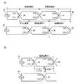
実施形態の2重ループ構造は、常時通電されている第1の給電ループとしての常用給電ループ3と通常は通電されていない予備的給電ループとしての役割をもつ第2の給電ループとしての待機給電ループ6とを備えて構成されている。尚、以下の説明では、高周波電源位置を始端とし待機ループの長軸方向端(ループの折り返し端)を終端として、高周波電源位置からループの折り返し端までの直線距離をループ長と呼ぶこととする(図1(a)参照)。
The double loop structure of the embodiment has a standby power supply as a second power supply loop having a role as a normal power supply loop 3 as a first power supply loop that is always energized and a standby power supply loop that is not normally energized. And a
また、2重ループ構造を構成する常用給電ループ3と待機給電ループ6の配置態様について図2を参照して説明する。図2(a)〜(c)は2重ループ構造を真上から見た図である。尚、図2(a)〜(c)は2重ループ構造の配置態様を説明するための図であるため便宜上常用給電ループ3に設けられている捻架点を省略している。
The arrangement of the normal power supply loop 3 and the standby
第1の態様として、例えば、図2(a)に示すように常用給電ループ3と待機給電ループ6が水平方向に所定間隔ずれて配置され、さらに常用給電ループ3の上に所定間隔をおいて待機給電ループ6が一部重なるように配置されている態様(以下、「一部重なり配置」と呼ぶ。)が挙げられる。
As a first mode, for example, as shown in FIG. 2A, the normal power supply loop 3 and the standby
第2の態様として、例えば、図2(b)に示すように常用給電ループ3と待機給電ループ6が水平方向にずれることなく常用給電ループ3の上に所定間隔をおいて待機給電ループ6が完全に重なるように配置されている態様(以下、「全重なり配置」と呼ぶ。)が挙げられる。
As a second mode, for example, as shown in FIG. 2B, the standby power supply loop 3 and the standby
尚、上記したループ同士が重なる配置態様以外にも、図2(c)に示すように常用給電ループ3と待機給電ループ6が重なることなく水平方向に所定間隔をおいて横並びで配置される態様(以下、「横並び配置」と呼ぶ。)でもよい。
In addition to the arrangement mode in which the loops overlap each other, as shown in FIG. 2C, the normal power supply loop 3 and the standby
以下の説明では、常用給電ループ3と待機給電ループ6の配置態様が一部重なり配置であるとして説明する。尚、後述する第2の実施の形態及び第3の実施の形態に関わる2重ループ構造においても2重ループの配置態様が一部重なり配置であるとして説明する。
In the following description, the arrangement modes of the normal power supply loop 3 and the standby
また、常用給電ループ3と待機給電ループ6としては、高周波電源に接続された閉ループ構造であり、例えば、楕円形状のループや略長方形状のループ等が挙げられる。また、常用給電ループ3と待機給電ループ6のループ長は等しい。
Further, the normal power supply loop 3 and the standby
常用給電ループ3は高周波電源2に接続されており、コンデンサC1,C2と、捻架点4を介してコンデンサC1に接続されたコンデンサC4と、捻架点4を介してコンデンサC2に接続されたコンデンサC3とを備えて構成されている。 The normal power supply loop 3 is connected to the high frequency power source 2, and is connected to the capacitors C 1 and C 2, the capacitor C 4 connected to the capacitor C 1 via the twist point 4, and the capacitor C 2 via the twist point 4. And a capacitor C3.
待機給電ループ6は高周波電源2と同一周波数の高周波電源5に接続され、コンデンサC5,C6を備えて構成されている。高周波電源5とコンデンサC5の間にはスイッチSWが設けられている。通常時にはスイッチSWはオフしており待機給電ループ6は通電されていない。
The standby
尚、図1(a)の例では、常用給電ループ3の捻架点4における捻りは180度捻り(1回捻り)である。180度捻りにする理由は、後述するように捻架点4から見て高周波電源2側(前側)における待機給電ループ6に与える磁界の向き(待機給電ループ6に誘起される誘起電圧の向き)と折り返し端側(後側)における待機給電ループ6に与える磁界の向き(待機給電ループ6に誘起される誘起電圧の向き)を互いに逆方向にできるからである。
In the example of FIG. 1A, the twist at the twisting point 4 of the regular feeding loop 3 is a 180 degree twist (one twist). The reason for twisting 180 degrees is the direction of the magnetic field applied to the standby
また、捻りは上記した1回捻り以外に奇数回(3回、5回、・・・)捻りであってもよい。奇数回捻りであれば上記1回捻りの場合と同様に捻架点4を境に待機給電ループ6に与える磁界の向きを逆方向にできるからである。
Further, the twist may be an odd number of times (3 times, 5 times,...) Twist other than the above-described one time twist. This is because if the number of turns is an odd number, the direction of the magnetic field applied to the standby
また、図1(a)に示す例では、捻架点4は常用給電ループ3のループ長の中間に配置されている。
ここで、常用給電ループ3は所定のインダクタンスLを有するコイルとしてみなすことができるので、高周波電源2からの交流電流が常用給電ループ3に流れると、常用給電ループ3から待機給電ループ6に誘起電圧が誘起される。待機給電ループ6に誘起される誘起電圧は、図1(b)に示すように、常用給電ループ3に接続された高周波電源2(始端)から捻架点4までの間では高周波電源2からの距離が長くなるにしたがって増大し、捻架点4から折り返し端(終端)までの間では高周波電源2からの距離が長くなるにしたがって減少する。
Further, in the example shown in FIG. 1A, the twist point 4 is arranged in the middle of the loop length of the regular power feeding loop 3.
Here, since the normal power supply loop 3 can be regarded as a coil having a predetermined inductance L, when an alternating current from the high frequency power supply 2 flows into the normal power supply loop 3, an induced voltage is generated from the normal power supply loop 3 to the standby
待機給電ループ6に誘起される誘起電圧が捻架点4から折り返し端までの間で減少する理由は、常用給電ループ3において、捻架点4から見て高周波電源2側(前側)における待機給電ループ6に与える磁界の向き(待機給電ループ6に誘起される誘起電圧の向き)と折り返し端側(後側)における待機給電ループ6に与える磁界の向きがそれぞれ逆方向になるからである。
The reason why the induced voltage induced in the standby
図1(a)の例では、捻架点4が常用給電ループ3のループ長の中間に配置されているので、始端から捻架点4までの待機給電ループ6に誘起される誘起電圧の増加分と捻架点4から終端までの該誘起電圧の減少分が同じになる。このためループの終端で待機給電ループ6に誘起される誘起電圧がちょうど零になる。
In the example of FIG. 1A, since the twisting point 4 is arranged in the middle of the loop length of the regular feeding loop 3, an increase in induced voltage induced in the
ここで、仮に常用給電ループ3が捻架されていない場合を考えると、待機給電ループ6に誘起される誘起電圧はループの始端から終端まで増加し続ける。
従って、常用給電ループ3が捻架されていない場合に比べて誘起電圧の増加を抑制することができる。
Here, if the case where the normal power supply loop 3 is not twisted is considered, the induced voltage induced in the standby
Therefore, an increase in induced voltage can be suppressed as compared with the case where the regular power feeding loop 3 is not twisted.
尚、図1(a)の例とは異なり、捻架点4が常用給電ループ3のループ長の中間に配置されていない場合、例えば、始端から捻架点4までの距離の方が捻架点4から終端までの距離よりも長い場合には、終端における待機給電ループ6に誘起される誘導電圧は完全に零にならない。この場合、誘起電圧の増加分と減少分が図1(b)の例のように完全に打ち消し合うことはないが、常用給電ループ3が捻架されていない場合に比べると待機給電ループ6に誘起される誘起電圧の増加を抑制することができる。
In addition, unlike the example of FIG. 1A, when the twisting point 4 is not arranged in the middle of the loop length of the normal power feeding loop 3, for example, the distance from the starting end to the twisting point 4 is the twisting direction. When the distance is longer than the distance from the point 4 to the terminal, the induced voltage induced in the
(変形例1)
図1に示した例では、待機用給電ループ6に対して常用給電ループ3のループ長の中間に1つの捻架点4を有して構成したものを示したが、常用給電ループ3に複数の捻架点(図示せず)を有して構成したものでもよい。
(Modification 1)
In the example shown in FIG. 1, the standby
具体的には、高周波電源2から最初の捻架点までの距離、及び、隣り合う捻架点間の距離が全て同じになるように常用給電ループ3の複数箇所に捻架点を設ける。
捻架点の設定方法は、具体的には、(1)まず、高周波電源2から所定の距離だけ離れた位置に最初の捻架点を設け、(2)最初の捻架点から次の捻架点までの距離、及び、以降の捻架点間の距離をループの終端に至るまで全て等間隔にするように捻架点を設ける。
Specifically, twist points are provided at a plurality of locations in the regular power supply loop 3 so that the distance from the high-frequency power source 2 to the first twist point and the distance between adjacent twist points are all the same.
Specifically, the method of setting the twist point is as follows: (1) First, the first twist point is provided at a position away from the high-frequency power source 2 by a predetermined distance, and (2) the next twist point is set to the next twist point. Twist points are provided so that the distance to the gantry point and the distance between the subsequent gyration points are all equally spaced until the end of the loop.
上記構成によれば、常用給電ループ3において、各捻架点から見て高周波電源2側(前側)における待機給電ループ6に与える磁界の向き(誘起電圧の向き)と折り返し端側(後側)における磁界の向き(誘起電圧の向き)がそれぞれ逆方向になるため各捻架点を境に捻架点の前側誘起電圧と後側誘起電圧が打ち消し合うことになる。
According to the above configuration, the direction of the magnetic field applied to the standby
このため、待機給電ループ6に誘起される誘起電圧が増加し続けることはない。従って、誘起電圧の増加を抑制することができる。
(変形例2)
上記第1の実施の形態に関わる2重ループ構造は、常用給電ループ3と常用給電ループ3から誘起電圧が誘起される待機給電ループ6とを備え、捻架点4を境に待機給電ループ6に与える磁界の向きを逆にするように常用給電ループ3が捻架された構成となっているが、常用給電ループと該常用給電ループから誘起電圧が誘起される待機給電ループとを備え、捻架点を境に常用給電ループから待機給電ループに与える磁界の向きを逆にするように待機給電ループが捻架された構成(図示せず)としてもよい。
For this reason, the induced voltage induced in the standby
(Modification 2)
The double loop structure according to the first embodiment includes a normal power supply loop 3 and a standby
このような構成でも、待機給電ループに誘起された誘起電圧は待機給電ループに接続された高周波電源から離れるにしたがって増加し続け捻架点を境に誘起電圧の向きが互いに逆方向となるので、待機給電ループの誘起電圧は捻架点を境に前記高周波電源から離れるにしたがって減少する。従って、誘起電圧の増加を抑制することができる。 Even in such a configuration, the induced voltage induced in the standby power supply loop continues to increase as the distance from the high-frequency power source connected to the standby power supply loop increases. The induced voltage of the standby power supply loop decreases as the distance from the high-frequency power source increases from the twisting point. Therefore, an increase in induced voltage can be suppressed.
[第2の実施形態]
以下に本発明の第2の実施形態について図3〜図6を参照して説明する。
本発明の第2の実施形態の2重ループ構造は、常時通電されている常用給電ループ38,43を2つ用いた形態である。
[Second Embodiment]
Hereinafter, a second embodiment of the present invention will be described with reference to FIGS.
The double loop structure of the second embodiment of the present invention is a form using two normal
ところで、高周波電源とコンデンサを有するループ構造においては共振を使ってできるだけ効率的に電流を流すことが必要である。ループそのものをコイルとみなした場合の誘導性リアクタンス(ωL)と容量性リアクタンス(1/ωC)を等しくさせる、いわゆる、共振条件(ωL=1/ωC)を満たせばループのインピーダンスを0にすることができるからである。共振条件を満たすときの周波数を共振周波数といい、この共振周波数は上記共振条件を満たすようにコイルのインダクタンスLとコンデンサの容量Cの値に応じて一義的に求められる。 By the way, in a loop structure having a high-frequency power source and a capacitor, it is necessary to flow current as efficiently as possible using resonance. When the loop itself is regarded as a coil, the inductive reactance (ωL) and the capacitive reactance (1 / ωC) are equalized, and so-called resonance condition (ωL = 1 / ωC) is satisfied, so that the loop impedance is reduced to zero. Because you can. A frequency when the resonance condition is satisfied is called a resonance frequency, and this resonance frequency is uniquely determined according to the values of the inductance L of the coil and the capacitance C of the capacitor so as to satisfy the resonance condition.
図6(a)は第1の実施形態における常用給電ループにおける共振周波数特性示したものである。最もインピーダンス(縦軸)が低いところ(円で囲んだ中の凸部分)の周波数f0が共振周波数となる。 FIG. 6A shows the resonance frequency characteristic in the normal power feeding loop in the first embodiment. The frequency f 0 where the impedance (vertical axis) is the lowest (the convex portion in the circle) is the resonance frequency.
ここで、図3に示すように常用給電ループ18,23を2つ備えた2重ループ構造であって、それぞれ常用給電ループ18,23に設けられた捻架点19,24が高周波電源17,22から同じ距離だけ離れた位置に設けられた2重ループ構造について検討する。
上記した2重ループ構造における共振周波数f0は、図6(a)に示すいわゆる1重ループ構造における共振周波数f0と比較するとずれてしまっていることがわかる。このため効率的に電流を流すことができなくなり集電できなくなる。
Here, as shown in FIG. 3, a double loop structure having two normal
It can be seen that the resonance frequency f 0 in the above-described double loop structure is deviated from the resonance frequency f 0 in the so-called single loop structure shown in FIG. For this reason, it becomes impossible to flow an electric current efficiently and to collect current.
共振周波数がずれてしまう理由は、常用給電ループを2つ備えた2重ループ構造とした場合には相互インダクタンスMの要素が追加されるからである。
以下に、相互インダクタンスMと共振周波数との関係について説明する。
The reason why the resonance frequency is shifted is that an element of mutual inductance M is added in the case of a double loop structure having two regular power supply loops.
The relationship between the mutual inductance M and the resonance frequency will be described below.
2重ループそれぞれに交流電源から交流電流を流すとそれぞれの給電ループに誘起電圧が発生する。2重ループ構造における常用給電ループ18,23の共振条件は、ωLを誘導性リアクタンス、Mを相互インダクタンス、1/ωCを容量性リアクタンスとすると、ω(L+M)=1/ωCとなる。
When an alternating current is supplied from an alternating current power source to each of the double loops, an induced voltage is generated in each power feeding loop. The resonance conditions of the
共振周波数f0は誘導性リアクタンスωL、容量性リアクタンス1/ωC及び相互インダクタンスMに基づいて決定されるため、2重ループ構造では常用給電ループ一つだけで構成される1重ループ構造の共振周波数(図6(a)参照)と比較すると相互インダクタンスMに影響される分だけ共振周波数がずれてしまう(図6(b)参照)。 Since the resonance frequency f 0 is determined based on the inductive reactance ωL, the capacitive reactance 1 / ωC, and the mutual inductance M, in the double loop structure, the resonance frequency of the single loop structure constituted by only one common feeding loop. Compared to (see FIG. 6A), the resonance frequency is shifted by the amount affected by the mutual inductance M (see FIG. 6B).
そこで、本第2の実施の形態では、図4(a)に示すように2つの常用給電ループ38,43における捻架点をずらすことにより上記した共振周波数のずれを無くしている。以下に、図4(a),(b)を参照してその原理を詳細に説明する。
Therefore, in the second embodiment, as shown in FIG. 4A, the above-described shift in the resonance frequency is eliminated by shifting the twisting points in the two normal
図4(a)に示すように、本実施形態の2重ループ構造は、高周波電源37に接続され通電されている常用給電ループ(第1の通電ループ)38と高周波電源42に接続され通電されている常用給電ループ(第2の通電ループ)43とで構成されている。尚、常用給電ループ38,43の配置態様は上記第1の実施の形態と同様に、一部重なり配置、全重なり配置、横並び配置が挙げられるが、以下では常用給電ループ38,43の配置態様が一部重なり配置(図5参照)であるとして説明する。
As shown in FIG. 4A, the double loop structure of the present embodiment is connected to a normal power supply loop (first energization loop) 38 connected to a high
常用給電ループ38には複数の捻架点39,40,41が設けられ、捻架点39と該捻架点39に隣接する捻架点40との間の第1の捻架区間A1の距離と捻架点40と該捻架点40に隣接する捻架点41との間の第2の捻架区間B1の距離とが同一の距離となるように捻架点39〜41が配置されている。
The
常用給電ループ43には捻架点45,46が設けられ、捻架点45と該捻架点45に隣接する捻架点46との間の第1の捻架区間C1の距離と捻架点46と常用給電ループ43の折り返し端との間の第2の捻架区間D1の距離とが同一の距離となるように捻架点45,46が配置されている。また、捻架区間A1〜D1の区間長はすべて同じである。
The
常用給電ループ43の捻架点45は、第2の通電ループとしての常用給電ループ43の捻架区間C1が常用給電ループ38の捻架区間Aに対して該常用給電ループ38の捻架区間A1の半分の距離(ずらし区間長)だけずれるように配置されている。常用給電ループ43の捻架点46は、常用給電ループ43の捻架区間D1が常用給電ループ38の捻架区間B1に対して該常用給電ループ38の捻架区間B1の半分の距離(ずらし区間長)だけずれるように配置されている。
The
尚、コンデンサC30,31は高周波電源37と捻架点39との間に設けられ、コンデンサC32,33は捻架点39と捻架点40の間に設けられ、コンデンサC34,35は捻架点40と捻架点41の間に設けられている。コンデンサC30〜C35は、常用給電ループ38の誘導性リアクタンス(ωL)を打ち消してループにおけるインピーダンスを零にするための容量性リアクタンス(ωC)を有する。
The capacitors C30 and 31 are provided between the high-
コンデンサC36,37は高周波電源42と捻架点45との間に設けられ、コンデンサC38,39は捻架点45と捻架点46の間に設けられ、コンデンサC40,41は捻架点46と常用給電ループ43の折り返し端との間に設けられ、常用給電ループ43の誘導性リアクタンスを打ち消してループにおけるインピーダンスを零にするための容量性リアクタンスを有する。
The capacitors C36 and 37 are provided between the high-
上記したように捻架点を配置することにより、例えば、常用給電ループ38から数えて最初の捻架点39を境に常用給電ループ38が常用給電ループ43に与える磁界の向きが逆方向に変わり、常用給電ループ42から数えて最初の捻架点45を境に常用給電ループ43が常用給電ループ38に与える磁界の向きが逆方向に変わる。
By arranging the twist points as described above, for example, the direction of the magnetic field that the
その後、常用給電ループ38の次の捻架点40を境に常用給電ループ38が常用給電ループ43に与える磁界の向きが逆方向に変わり、常用給電ループ43の次の捻架点46を境に常用給電ループ43が常用給電ループ38に与える磁界の向きが逆方向に変わり、以降は、上記動作が常用給電ループ38及び常用給電ループ43の長軸方向端まで繰り返される。
Thereafter, the direction of the magnetic field applied to the normal
このため、常用給電ループ38の各捻架点39,40,41を境に常用給電ループ43に誘起される誘起電圧が完全に打ち消し合うとともに常用給電ループ43の各捻架点45,46を境に常用給電ループ38に誘起される誘起電圧が完全に打ち消し合い、相互インダクタンスMが零であるのと同様の状態になる。
For this reason, the induced voltages induced in the normal
以下に相互インダクタンスMの値が零になる原理について図4(b)を参照して説明する。
例えば、給電ループ43に流れる電流をI、給電ループ38と給電ループ43の相互インダクタンスをM、角周波数を2πf(ω)、捻架点39から給電ループ38における捻架点45に対応する位置までの距離をL1、該対応位置から捻架点40までの距離をL2とすると、距離L1にて給電ループ43から給電ループ38に誘起される誘起電圧E1は2πfMIL1であり、距離L2にて給電ループ43から給電ループ38に誘起される誘起電圧E2は2πfMIL2である。
Hereinafter, the principle that the value of the mutual inductance M becomes zero will be described with reference to FIG.
For example, the current flowing through the
捻架点45を境に給電ループ38に誘起される誘起電圧E1と誘起電圧E2の向きは逆向きになるので、距離L(=L1+L2)にて給電ループ43から給電ループ38に誘起される誘起電圧E(E1+E2)は2πfMI(L1−L2)となる。
Since the induced voltage E 1 and the induced voltage E 2 induced in the
このため、L1とL2が同じ距離の場合には相互インダクタンスMが零であるのと同様の状態になり、共振条件はω(L+M)=1/ωCではなくωL=1/ωCとなる。
従って、本第2の実施の形態では図6(c)に示すように共振周波数のずれを確実になくすことができる。
For this reason, when L 1 and L 2 are the same distance, the mutual inductance M is in the same state as zero, and the resonance condition is not ω (L + M) = 1 / ωC but ωL = 1 / ωC. .
Therefore, in the second embodiment, the resonance frequency shift can be reliably eliminated as shown in FIG.
(変形例1)
尚、図4(a),(b)の例では、捻架区間Cが捻架区間Aに対して捻架区間Aの距離の半分の距離だけずれるように捻架点45が配置されているが、ずらす距離は捻架区間Aの半分でなくてもよい。
(Modification 1)
4A and 4B, the
この場合、常用給電ループ38の各捻架点39,40,41を境に常用給電ループ43に誘起される誘起電圧が所定量だけ打ち消し合うとともに常用給電ループ38の各捻架点45,46を境に常用給電ループ38に誘起される誘起電圧が所定量だけ打ち消し合う。
In this case, the induced voltages induced in the normal
本変形例では、上記した数式E=2πfMI(L1−L2)の中の(L1−L2)が完全に零にならない場合である。このため相互インダクタンスMの値を零にすることはできないが、(L1−L2)を1より小さい値にするようにずらす距離を設定すれば、全くずらさない場合と比較して相互インダクタンスMの値を軽減することができ、共振周波数のずれの量を軽減できる。 In this modification, a case where the above-mentioned equation E = 2πfMI (L 1 -L 2 ) of the inside (L 1 -L 2) is not completely zero. For this reason, the value of the mutual inductance M cannot be made zero, but if the distance for shifting (L 1 −L 2 ) is set to a value smaller than 1, the mutual inductance M is compared with the case of not shifting at all. The value of can be reduced, and the amount of deviation of the resonance frequency can be reduced.
[第3の実施形態]
以下に本発明の第3の実施形態について図7を参照して説明する。
上記第3の実施形態における2重ループ構造については、上記した図4に示したものと同じであるのでその説明は省略する。
[Third embodiment]
A third embodiment of the present invention will be described below with reference to FIG.
Since the double loop structure in the third embodiment is the same as that shown in FIG. 4 described above, the description thereof is omitted.
上記した第2の実施形態では、高周波電源37から最初の捻架点39までの区間A2(捻架点39を含めず)において常用給電ループ38に流れる第1の電流の位相を0度とし、常用給電ループ43に流れる第2の電流の位相を0度とする。第1の電流及び第2の電流の位相は同じ(0度)であるので第1の電流と第2の電流の合成電流振幅が2倍となり区間Aでは集電が可能となる(図7(a)参照)。
In the second embodiment described above, the phase of the first current flowing in the normal
ところが、最初の捻架点39から常用給電ループ43の最初の捻架点45までの区間B2(捻架点45を含めず)では第1の電流の位相が180度となり、第1の電流の位相と第2の電流の位相の差が180度となるため第1の電流と第2の合成電流振幅が零となり区間B2では集電できない(図7(a)参照)。
However, in the section B2 (not including the twist point 45) from the
常用給電ループ43の最初の捻架点45から常用給電ループ38の次の捻架点40までの区間C2(捻架点40を含めず)では、第1の電流の位相は180度のままであり、第2の電流の位相が180度となり、常用給電ループ38と常用給電ループ43における電流の位相が同じになるので第1の電流と第2の電流の合成電流振幅が2倍となり区間C2では集電が可能となる。常用給電ループ38の捻架点40から常用給電ループ43の次の捻架点46までの区間(区間D2)は集電不能、常用給電ループ43の捻架点46から常用給電ループ38の捻架点41までの区間(区間E2)は集電可能、常用給電ループ38の捻架点41から長軸方向端までの区間(区間F2)は集電不能となる。
In the section C2 (not including the twist point 40) from the
本第3の実施の形態による2重ループ構造によれば、後述する方法で上記した集電不能期間をなくすことによって、より安定した集電(電力供給)を行うことができる。以下に、集電不能期間をなくす原理について図7を参照して詳細に説明する。 According to the double loop structure according to the third embodiment, more stable current collection (power supply) can be performed by eliminating the above-described current collection impossible period by a method described later. Hereinafter, the principle of eliminating the current collection impossible period will be described in detail with reference to FIG.
本第3の実施の形態では、高周波電源37,42に電流位相制御部50が接続されている。電流位相制御部50は常用給電ループ38に流れる電流(第1の電流)と常用給電ループ43に流れる電流(第2の電流)との位相差が常に90度になるように高周波電源37,42を制御している。
In the third embodiment, a current
(区間A2における集電)
高周波電源37から最初の捻架点39までの区間A2(捻架点39を含めず)において常用給電ループ38に流れる第1の電流の位相(α度)と第2の電流の位相(β度)との差(β−α)は90度であるので第1の電流と第2の電流の合成電流振幅が2倍となり区間A2では集電が可能となる(図7(a)参照)。
(Current collection in section A2)
The phase (α degree) of the first current and the phase (β degree) of the first current flowing through the
このため、区間A2における集電量(集電電流)の大きさ(第1の電流と第2の電流の合成電流振幅)を算出すると、常用給電ループ38単独若しくは常用給電ループ43単独で集電可能な集電量(基準集電量)のおよそ1.4(√2)倍の集電量が得られる。
For this reason, if the magnitude of the current collection amount (current collection current) in the section A2 (combined current amplitude of the first current and the second current) is calculated, current can be collected by the normal
(区間B2における集電)
最初の捻架点39から常用給電ループ43の最初の捻架点45までの区間B2(捻架点45を含めず)では第1の電流の位相が(α+180)度であり、第2の電流の位相はβ度のままであるので、第1の電流の位相(α+180)と第2の電流の位相(β)との差は90度のままである。
(Current collection in section B2)
In a section B2 (not including the twist point 45) from the
このため、区間B2における集電量(集電電流)の大きさ(第1の電流と第2の電流の合成電流振幅)を算出すると、常用給電ループ38単独若しくは常用給電ループ43単独で集電可能な集電量(基準集電量)のおよそ1.4(√2)倍の集電量が得られる。
For this reason, when the magnitude of the current collection amount (current collection current) in the section B2 (combined current amplitude of the first current and the second current) is calculated, current can be collected by the normal
(区間C2における集電)
常用給電ループ43の捻架点45から常用給電ループ38の次の捻架点40までの区間C(捻架点40を含めず)では第1の電流の位相が(α+180)度のままであり、第2の電流の位相は(β+180)度となるので、第1の電流の位相(α+180)と第2の電流の位相(β+180)との差は90度のままである。
(Current collection in section C2)
In the section C (not including the twist point 40) from the
このため、区間C2における集電量(集電電流)の大きさ(第1の電流と第2の電流の合成電流振幅)を算出すると、常用給電ループ38単独若しくは常用給電ループ43単独で集電可能な集電量(基準集電量)のおよそ1.4(√2)倍の集電量が得られる。以降の区間D2〜F2は上記動作が繰り返され常時基準集電量の1.4倍の集電量が得られる。区間D2〜F2については上記区間B2、区間C2と同様の動作が行われるので説明は省略する。
For this reason, when the magnitude of the current collection amount (current collection current) in the section C2 (combined current amplitude of the first current and the second current) is calculated, current can be collected by the normal
このため、第1の電流と第2の電流の位相差は常用給電ループ38及び常用給電ループ43のいずれの区間であっても常に90度を保つことができ集電が可能となる。
従って、本第3の実施の形態によれば、集電不能期間をなくすことができ常に1.4倍の集電動作が繰り返されることにより安定した電力供給を行うことができる。
For this reason, the phase difference between the first current and the second current can always be maintained at 90 degrees in any section of the normal
Therefore, according to the third embodiment, it is possible to eliminate the period during which current cannot be collected and to stably supply power by constantly repeating the current collection operation by 1.4 times.
(変形例1)
また、上記第3の実施の形態では、電流位相制御部50は、第1の電流と第2の電流の位相差が常に90度となるように常用給電ループ38及び常用給電ループ43を制御していたが、常用給電ループ38に流れる第1の電流の位相だけを常用給電ループ43に流れる第2の電流の位相に対して90度ずらすように高周波電源37のみを制御してもよい。この場合、電流位相制御部50は高周波電源37にのみ接続される。
(Modification 1)
In the third embodiment, the
また、常用給電ループ43に流れる第2の電流の位相だけを常用給電ループ38に流れる第1の電流の位相に対して90度ずらすように高周波電源42のみを制御してもよい。この場合、電流位相制御部50は高周波電源42にのみ接続される。
Alternatively, only the high
(変形例2)
尚、90度電流位相をずらすように制御することによって常に基準集電量の1.4倍の集電を可能にしているが、90度以外の電流位相でずらした場合でも区間ごとの集電量にバラツキが生じるものの集電不能期間をなくすという効果を得ることができる。
(Modification 2)
In addition, by controlling the current phase to be shifted by 90 degrees, it is possible to collect current 1.4 times the reference current collection amount. However, even if the current phase is shifted by other than 90 degrees, the current collection amount for each section is reduced. Although variation occurs, an effect of eliminating the non-collection period can be obtained.
ここで、本実施形態においては、高周波電源2,37が本発明の第1の高周波電源に相当し、高周波電源5,42が本発明の第2の高周波電源に相当し、常用給電ループ3が本発明請求項1〜6の第1の給電ループに相当し、待機給電ループ6が本発明請求項1〜6の第2の給電ループに相当し、常用給電ループ38が本発明請求項7〜9の第1の給電ループに相当し、常用給電ループ43が本発明請求項7〜9の第2の給電ループに相当する。
Here, in the present embodiment, the high-
以上本発明の一実施形態について説明したが、本発明は、上記実施形態に限定されるものではなく、本発明の要旨を逸脱しない範囲内にて種々の態様をとることができる。 Although one embodiment of the present invention has been described above, the present invention is not limited to the above-described embodiment, and can take various forms without departing from the gist of the present invention.
2,5,37,42…高周波電源、3,38,43…常用給電ループ、4,39,40,41,45,46…捻架点、6…待機給電ループ。 2, 5, 37, 42 ... high frequency power source, 3, 38, 43 ... regular feeding loop, 4, 39, 40, 41, 45, 46 ... twisting point, 6 ... standby feeding loop.
Claims (7)
第2の高周波電源に接続され前記第1の給電ループから誘起電圧が誘起される第2の給電ループとを備え、
前記第1の高周波電源から所定の距離を置いて少なくとも1つの捻架点があり、該捻架点を境に前記第2の給電ループに対して与える磁界の向きを逆にするように前記第1の給電ループが捻架されている
ことを特徴とする2重ループ構造。 A first feeding loop connected to the first high frequency power source and energized;
A second power supply loop connected to a second high-frequency power source and inducing an induced voltage from the first power supply loop;
There is at least one twist point at a predetermined distance from the first high-frequency power source, and the first magnetic field applied to the second feeding loop is reversed at the twist point. A double loop structure characterized in that one feeding loop is twisted.
第2の高周波電源に接続され前記第1の給電ループから誘起電圧が誘起される第2の給電ループとを備え、
前記第2の高周波電源から所定の距離を置いて少なくとも1つの捻架点があり、該捻架点を境に前記第2の給電ループに与える磁界の向きを逆にするように前記第2の給電ループが捻架されている
ことを特徴とする2重ループ構造。 A first feeding loop connected to the first high frequency power source and energized;
A second power supply loop connected to a second high-frequency power source and inducing an induced voltage from the first power supply loop;
There is at least one twist point at a predetermined distance from the second high-frequency power source, and the second magnetic field applied to the second feeding loop is reversed with the twist point as a boundary. A double loop structure characterized in that the feed loop is twisted.
ことを特徴とする請求項1に記載の2重ループ構造。 The double loop structure according to claim 1, wherein a plurality of twist points are provided in the first power feeding loop, and the distances between the adjacent twist points are equal.
ことを特徴とする請求項2に記載の2重ループ構造。 The double loop structure according to claim 2, wherein a plurality of twist points are provided in the second feeding loop, and the distances between the adjacent twist points are equally spaced.
第2の高周波電源に接続され通電された第2の給電ループとを備え、
前記第1の給電ループに複数の捻架点が設けられ、
前記第2の給電ループに複数の捻架点が設けられ、前記第1の給電ループの隣り合う捻架点間に対応させて前記第2の給電ループの捻架点が一つ配置され、
前記第1の給電ループの各捻架点を境に前記第1の給電ループから前記第2の給電ループに与える磁界の向きを逆にするように前記第1の給電ループが捻架され、
前記第2の給電ループの各捻架点を境に前記第2の給電ループから前記第1の給電ループに与える磁界の向きを逆にするように前記第2の給電ループが捻架されている
ことを特徴とする2重ループ構造。 A first feeding loop connected to the first high frequency power source and energized;
A second feeding loop connected to the second high frequency power source and energized,
A plurality of twist points are provided in the first feeding loop,
A plurality of twisting points are provided in the second power feeding loop, and one twisting point of the second power feeding loop is arranged in correspondence between adjacent twisting points of the first power feeding loop,
The first power supply loop is twisted so that the direction of the magnetic field applied from the first power supply loop to the second power supply loop is reversed at each twist point of the first power supply loop,
The second power supply loop is twisted so that the direction of the magnetic field applied from the second power supply loop to the first power supply loop is reversed at each twist point of the second power supply loop. A double loop structure characterized by that.
前記第1の給電ループの隣り合う捻架点と捻架点の中間に対応させて前記第2の給電ループの捻架点が配置された
ことを特徴とする請求項5に記載の2重ループ構造。 The distance between adjacent twist points of the first feeding loop is the same;
6. The double loop according to claim 5, wherein the twist point of the second power supply loop is disposed so as to correspond to an intermediate position between adjacent twist points of the first power supply loop. Construction.
ことを特徴とする請求項5又は6に記載の2重ループ構造。 The current phase control unit that further sets a phase difference between the first current flowing through the first power feeding loop and the second current flowing through the second power feeding loop to 90 degrees. 6. A double loop structure according to 6.
Priority Applications (2)
| Application Number | Priority Date | Filing Date | Title |
|---|---|---|---|
| JP2010293401A JP2012143061A (en) | 2010-12-28 | 2010-12-28 | Double loop structure |
| US13/333,435 US20120161520A1 (en) | 2010-12-28 | 2011-12-21 | Double loop structure |
Applications Claiming Priority (1)
| Application Number | Priority Date | Filing Date | Title |
|---|---|---|---|
| JP2010293401A JP2012143061A (en) | 2010-12-28 | 2010-12-28 | Double loop structure |
Publications (1)
| Publication Number | Publication Date |
|---|---|
| JP2012143061A true JP2012143061A (en) | 2012-07-26 |
Family
ID=46315727
Family Applications (1)
| Application Number | Title | Priority Date | Filing Date |
|---|---|---|---|
| JP2010293401A Pending JP2012143061A (en) | 2010-12-28 | 2010-12-28 | Double loop structure |
Country Status (2)
| Country | Link |
|---|---|
| US (1) | US20120161520A1 (en) |
| JP (1) | JP2012143061A (en) |
Cited By (1)
| Publication number | Priority date | Publication date | Assignee | Title |
|---|---|---|---|---|
| JP7438193B2 (en) | 2018-08-24 | 2024-02-26 | イーサーダイン テクノロジーズ インコーポレイテッド | Large area power transmitter for wireless power transfer |
Families Citing this family (13)
| Publication number | Priority date | Publication date | Assignee | Title |
|---|---|---|---|---|
| CN105656024B (en) * | 2015-12-02 | 2018-05-15 | 国电南瑞科技股份有限公司 | Electric power system operation standby margin of safety online evaluation method |
| US11862984B2 (en) | 2021-11-03 | 2024-01-02 | Nucurrent, Inc. | Wireless power receiver with repeater for enhanced power harvesting |
| US11848566B2 (en) | 2021-11-03 | 2023-12-19 | Nucurrent, Inc. | Dual communications demodulation of a wireless power transmission system having an internal repeater |
| US11831177B2 (en) | 2021-11-03 | 2023-11-28 | Nucurrent, Inc. | Wireless power transmitter with internal repeater and enhanced uniformity |
| US11962337B2 (en) | 2021-11-03 | 2024-04-16 | Nucurrent, Inc. | Communications demodulation in wireless power transmission system having an internal repeater |
| US11824372B2 (en) | 2021-11-03 | 2023-11-21 | Nucurrent, Inc. | Wireless power transmission antenna with puzzled antenna molecules |
| US11831173B2 (en) | 2021-11-03 | 2023-11-28 | Nucurrent, Inc. | Wireless power transmission antenna with series coil molecule configuration |
| US11831176B2 (en) | 2021-11-03 | 2023-11-28 | Nucurrent, Inc. | Wireless power transfer systems with substantial uniformity over a large area |
| US11824373B2 (en) | 2021-11-03 | 2023-11-21 | Nucurrent, Inc. | Wireless power transmission antenna with parallel coil molecule configuration |
| US11831175B2 (en) * | 2021-11-03 | 2023-11-28 | Nucurrent, Inc. | Wireless power transmission antenna with antenna molecules |
| US11955819B2 (en) | 2021-11-03 | 2024-04-09 | Nucurrent, Inc. | Communications modulation in wireless power receiver with multi-coil receiver antenna |
| US11824371B2 (en) | 2021-11-03 | 2023-11-21 | Nucurrent, Inc. | Wireless power transmission antenna with internal repeater and repeater filter |
| US11862991B2 (en) | 2021-11-03 | 2024-01-02 | Nucurrent, Inc. | Wireless power transmission antenna with internal repeater and in-coil tuning |
Citations (6)
| Publication number | Priority date | Publication date | Assignee | Title |
|---|---|---|---|---|
| JPS6416748U (en) * | 1987-07-22 | 1989-01-27 | ||
| JP2001270608A (en) * | 2000-03-24 | 2001-10-02 | Hitachi Kokusai Electric Inc | Article control rack |
| JP2002002917A (en) * | 2000-06-22 | 2002-01-09 | Hitachi Kokusai Electric Inc | Article control shelf |
| US6499701B1 (en) * | 1999-07-02 | 2002-12-31 | Magnemotion, Inc. | System for inductive transfer of power, communication and position sensing to a guideway-operated vehicle |
| JP2005026989A (en) * | 2003-07-01 | 2005-01-27 | Toshiba Corp | Antenna device and non-contact ic card reader/writer |
| JP2006025363A (en) * | 2004-07-09 | 2006-01-26 | Nippon Signal Co Ltd:The | Antenna for reader writer and article management system |
Family Cites Families (4)
| Publication number | Priority date | Publication date | Assignee | Title |
|---|---|---|---|---|
| ES2122209T3 (en) * | 1993-07-13 | 1998-12-16 | Actron Entwicklungs Ag | ANTENNA DEVICE. |
| US6118378A (en) * | 1997-11-28 | 2000-09-12 | Sensormatic Electronics Corporation | Pulsed magnetic EAS system incorporating single antenna with independent phasing |
| US6433272B1 (en) * | 2000-09-19 | 2002-08-13 | Storage Technology Corporation | Crosstalk reduction in constrained wiring assemblies |
| US7903777B1 (en) * | 2004-03-03 | 2011-03-08 | Marvell International Ltd. | System and method for reducing electromagnetic interference and ground bounce in an information communication system by controlling phase of clock signals among a plurality of information communication devices |
-
2010
- 2010-12-28 JP JP2010293401A patent/JP2012143061A/en active Pending
-
2011
- 2011-12-21 US US13/333,435 patent/US20120161520A1/en not_active Abandoned
Patent Citations (6)
| Publication number | Priority date | Publication date | Assignee | Title |
|---|---|---|---|---|
| JPS6416748U (en) * | 1987-07-22 | 1989-01-27 | ||
| US6499701B1 (en) * | 1999-07-02 | 2002-12-31 | Magnemotion, Inc. | System for inductive transfer of power, communication and position sensing to a guideway-operated vehicle |
| JP2001270608A (en) * | 2000-03-24 | 2001-10-02 | Hitachi Kokusai Electric Inc | Article control rack |
| JP2002002917A (en) * | 2000-06-22 | 2002-01-09 | Hitachi Kokusai Electric Inc | Article control shelf |
| JP2005026989A (en) * | 2003-07-01 | 2005-01-27 | Toshiba Corp | Antenna device and non-contact ic card reader/writer |
| JP2006025363A (en) * | 2004-07-09 | 2006-01-26 | Nippon Signal Co Ltd:The | Antenna for reader writer and article management system |
Cited By (1)
| Publication number | Priority date | Publication date | Assignee | Title |
|---|---|---|---|---|
| JP7438193B2 (en) | 2018-08-24 | 2024-02-26 | イーサーダイン テクノロジーズ インコーポレイテッド | Large area power transmitter for wireless power transfer |
Also Published As
| Publication number | Publication date |
|---|---|
| US20120161520A1 (en) | 2012-06-28 |
Similar Documents
| Publication | Publication Date | Title |
|---|---|---|
| JP2012143061A (en) | Double loop structure | |
| JP4689290B2 (en) | Method and apparatus for significantly reducing electrical ground displacement current generated by winding components | |
| CN107276447B (en) | More bridge topologys | |
| JP5215662B2 (en) | Power line filter | |
| JP2015056940A (en) | Multi-phase power conversion device filter circuit and multi-phase power conversion device | |
| JP6124336B2 (en) | Power supply device | |
| CN107769579A (en) | High pressure generator for X-ray equipment | |
| CN106655778B (en) | Multi output exchange type power converter | |
| JP2011109882A (en) | Drive circuit of vibration type actuator | |
| JP2014224493A (en) | Ignition device | |
| CN102208243A (en) | Inductor | |
| EP2388657A1 (en) | Apparatus and method to control temperature of heating roller used in fusing device of image forming apparatus | |
| CN102130595B (en) | Rear preregulator DC/DC converter | |
| JP2013505692A (en) | Inductor conductor for non-contact energy transmission and its use for vehicles | |
| EP3212923A1 (en) | Ignition system for an internal combustion engine and a control method thereof | |
| JP2015050777A (en) | Voltage transformer | |
| EP2632036A1 (en) | Small size power supply | |
| JP5927583B2 (en) | Contactless power supply system | |
| JP2009516999A (en) | Devices for connection to impedances with predominantly inductive properties | |
| JP5219219B2 (en) | Transformer and switching power supply device using the transformer | |
| JP4948388B2 (en) | Induction heating cooker | |
| JPWO2018199223A1 (en) | Power supply circuit | |
| CN107112835B (en) | The stator of motor | |
| JP2015527034A (en) | Parallel inverter connected to one inductor | |
| CN104972203A (en) | Method for regulating a welding power source |
Legal Events
| Date | Code | Title | Description |
|---|---|---|---|
| A621 | Written request for application examination |
Free format text: JAPANESE INTERMEDIATE CODE: A621 Effective date: 20131114 |
|
| A977 | Report on retrieval |
Free format text: JAPANESE INTERMEDIATE CODE: A971007 Effective date: 20140716 |
|
| A131 | Notification of reasons for refusal |
Free format text: JAPANESE INTERMEDIATE CODE: A131 Effective date: 20140819 |
|
| A02 | Decision of refusal |
Free format text: JAPANESE INTERMEDIATE CODE: A02 Effective date: 20141216 |