JP2012137839A - Memory control device and memory control method - Google Patents
Memory control device and memory control method Download PDFInfo
- Publication number
- JP2012137839A JP2012137839A JP2010288176A JP2010288176A JP2012137839A JP 2012137839 A JP2012137839 A JP 2012137839A JP 2010288176 A JP2010288176 A JP 2010288176A JP 2010288176 A JP2010288176 A JP 2010288176A JP 2012137839 A JP2012137839 A JP 2012137839A
- Authority
- JP
- Japan
- Prior art keywords
- element data
- written
- signal
- bank
- order
- Prior art date
- Legal status (The legal status is an assumption and is not a legal conclusion. Google has not performed a legal analysis and makes no representation as to the accuracy of the status listed.)
- Granted
Links
Images


Classifications
-
- G—PHYSICS
- G06—COMPUTING; CALCULATING OR COUNTING
- G06F—ELECTRIC DIGITAL DATA PROCESSING
- G06F9/00—Arrangements for program control, e.g. control units
- G06F9/06—Arrangements for program control, e.g. control units using stored programs, i.e. using an internal store of processing equipment to receive or retain programs
- G06F9/30—Arrangements for executing machine instructions, e.g. instruction decode
- G06F9/30098—Register arrangements
- G06F9/30105—Register structure
- G06F9/30109—Register structure having multiple operands in a single register
-
- G—PHYSICS
- G06—COMPUTING; CALCULATING OR COUNTING
- G06F—ELECTRIC DIGITAL DATA PROCESSING
- G06F9/00—Arrangements for program control, e.g. control units
- G06F9/06—Arrangements for program control, e.g. control units using stored programs, i.e. using an internal store of processing equipment to receive or retain programs
- G06F9/30—Arrangements for executing machine instructions, e.g. instruction decode
- G06F9/30003—Arrangements for executing specific machine instructions
- G06F9/3004—Arrangements for executing specific machine instructions to perform operations on memory
- G06F9/30043—LOAD or STORE instructions; Clear instruction
-
- G—PHYSICS
- G06—COMPUTING; CALCULATING OR COUNTING
- G06F—ELECTRIC DIGITAL DATA PROCESSING
- G06F9/00—Arrangements for program control, e.g. control units
- G06F9/06—Arrangements for program control, e.g. control units using stored programs, i.e. using an internal store of processing equipment to receive or retain programs
- G06F9/30—Arrangements for executing machine instructions, e.g. instruction decode
- G06F9/34—Addressing or accessing the instruction operand or the result ; Formation of operand address; Addressing modes
- G06F9/345—Addressing or accessing the instruction operand or the result ; Formation of operand address; Addressing modes of multiple operands or results
- G06F9/3455—Addressing or accessing the instruction operand or the result ; Formation of operand address; Addressing modes of multiple operands or results using stride
Abstract
Description
本発明は、メモリに対するデータの読み書きを制御するメモリ制御装置等に関する。 The present invention relates to a memory control device that controls reading and writing of data from and to a memory.
配列をなす大量の要素データに対し一定の演算を繰り返すベクトル処理において、ベクトルプロセッサが用いられる(たとえば、特許文献1)。ベクトルプロセッサによれば、一命令により配列の要素データを連続的に処理することで、高い演算スループットを得ることができる。ベクトルプロセッサは、たとえば、ロード・ストア用、演算用のパイプラインを有する。ロード・ストアパイプラインは、要素データをデータメモリから読み出して、演算パイプラインによる処理順序でレジスタ(以下、ベクトルレジスタという)に格納する。演算パイプラインは、演算命令のフェッチ、デコードを一回的に行い、ベクトルレジスタから要素データを順次連続して読み出し、算術演算などの演算を実行する。そして、演算パイプラインは、演算結果を示す要素データを処理順序でベクトルレジスタに格納する。そして、ロード・ストアパイプラインは、演算結果を示す要素データをレジスタから読み出し、処理順序でデータメモリに格納する。 A vector processor is used in vector processing that repeats certain operations on a large amount of element data forming an array (for example, Patent Document 1). According to the vector processor, it is possible to obtain a high calculation throughput by continuously processing the element data of the array with one instruction. The vector processor has, for example, pipelines for load / store and calculation. The load / store pipeline reads the element data from the data memory and stores it in a register (hereinafter referred to as a vector register) in the processing order of the operation pipeline. The arithmetic pipeline fetches and decodes arithmetic instructions once, sequentially reads element data from the vector register, and executes arithmetic operations and the like. Then, the operation pipeline stores the element data indicating the operation result in the vector register in the processing order. The load / store pipeline reads the element data indicating the operation result from the register and stores it in the data memory in the processing order.
たとえばDRAM(Dynamic Random Access Memory)などの大容量のデータメモリにおいて、入力用の要素データが不連続なアドレスに格納されている場合がある。あるいは、演算結果を示す要素データを、データメモリの不連続なアドレスに格納する場合がある。すると、ロード・ストアパイプラインが要素データをデータメモリからベクトルレジスタに読み出すとき、またはベクトルレジスタからデータメモリに書き込むときに、広範なメモリ領域へのアクセスが発生する。このことはレイテンシを増大させ、スループットを圧迫する要因となる。また、たとえば、データメモリとベクトルレジスタの間にSRAM(Static Random Access Memory)などの高速のキャッシュメモリを設けてパイプライン化し、これによりレイテンシを緩和しようとした場合、回路規模の増大や高コスト化を招くおそれがある。 For example, in a large-capacity data memory such as a DRAM (Dynamic Random Access Memory), element data for input may be stored at discontinuous addresses. Alternatively, element data indicating the calculation result may be stored at discontinuous addresses in the data memory. Then, when the load / store pipeline reads element data from the data memory to the vector register or writes data from the vector register to the data memory, an access to a wide memory area occurs. This increases the latency and becomes a factor of pressing the throughput. In addition, for example, when a high-speed cache memory such as SRAM (Static Random Access Memory) is provided between the data memory and the vector register to create a pipeline, thereby reducing the latency, the circuit scale increases and the cost increases. May be incurred.
本発明の目的は、データメモリの不連続なアドレスにアクセスして要素データを読み書きする場合であっても、最小限の回路構成により良好なスループットを得ることができるメモリ制御装置、及びメモリ制御方法を提供することにある。 An object of the present invention is to provide a memory control device and a memory control method capable of obtaining good throughput with a minimum circuit configuration even when reading and writing element data by accessing discontinuous addresses in a data memory Is to provide.
上記の目的を達成するために、第1の側面におけるメモリ制御装置は、読出しアドレスの入力に応答して複数の要素データを有する要素データ列が読み出される複数のバンクを有するメモリから、前記要素データ列を読み出すためのバンクごとの前記読出しアドレスを生成する第1の生成部と、前記要素データ列における選択すべき要素データの位置を示す位置信号と、前記選択すべき要素データをレジスタに格納する格納順序を示す順序信号とを生成する第2の生成部と、前記複数のバンクからそれぞれ読み出された前記要素データ列から前記位置信号に基づいて前記選択すべき要素データを選択し、当該選択した要素データを前記順序信号が示す格納順序で前記レジスタに格納するセレクタ部とを有し、前記レジスタに格納された要素データは、前記格納順序でベクトルプロセッサに処理される。 In order to achieve the above object, the memory control device according to the first aspect of the present invention is configured to provide the element data from a memory having a plurality of banks from which element data strings having a plurality of element data are read in response to input of a read address. A first generation unit that generates the read address for each bank for reading a column, a position signal indicating a position of element data to be selected in the element data string, and the element data to be selected are stored in a register. A second generation unit for generating an order signal indicating a storage order; and selecting the element data to be selected based on the position signal from the element data string read from each of the plurality of banks, and the selection And a selector unit for storing the element data stored in the register in the storage order indicated by the order signal. Data is processed in the vector processor in the storage order.
また、第2の側面におけるメモリ制御装置は、複数の要素データを有する要素データ列が、入力された書込みアドレスに書き込まれる複数のバンクを有するメモリに、前記要素データ列を書き込むためのバンクごとの書込みアドレスを生成する第1の生成部と、ベクトルプロセッサによる処理順序でレジスタに格納された、前記メモリに書き込むべき要素データの当該レジスタにおける格納順序を示す順序信号と、前記複数のバンクにそれぞれ書き込まれる要素データ列に前記書き込むべき要素データを挿入する位置を示す位置信号とを生成する第2の生成部と、前記複数のバンクに書き込まれる要素データ列における前記位置信号が示す位置に、前記順序信号が示す順序で前記書き込むべき要素データを挿入するセレクタ部とを有し、前記書き込むべき要素データ列が格納された要素データ列が、前記バンクごとの書込みアドレスに書き込まれる。 Further, the memory control device according to the second aspect is provided for each bank for writing the element data string in a memory having a plurality of banks in which the element data string having a plurality of element data is written to the input write address. A first generation unit for generating a write address; an order signal indicating the storage order in the register of the element data to be written to the memory, stored in a register in the processing order of the vector processor; and writing to each of the plurality of banks A second generation unit that generates a position signal indicating a position at which the element data to be written is inserted into the element data string to be written, and a position indicated by the position signal in the element data string to be written in the plurality of banks. A selector unit for inserting the element data to be written in the order indicated by the signal, and Element data string to burn them are stored element data string is written into the write address for each of the banks.
以下で説明する実施形態によれば、データメモリの不連続なアドレスにアクセスして要素データを読み書きする場合であっても、最小限の回路構成により良好なスループットを得ることができる。 According to the embodiments described below, even when accessing discontinuous addresses in the data memory to read / write element data, good throughput can be obtained with a minimum circuit configuration.
以下、図面にしたがって実施の形態について説明する。但し、適用される技術的範囲はこれらの実施の形態に限定されず、特許請求の範囲に記載された事項とその均等物まで及ぶものである。 Hereinafter, embodiments will be described with reference to the drawings. However, the applied technical scope is not limited to these embodiments, but extends to the matters described in the claims and equivalents thereof.
図1は、本実施形態が適用されるベクトルプロセッサの構成を説明する図である。 FIG. 1 is a diagram illustrating the configuration of a vector processor to which the present embodiment is applied.
ベクトルプロセッサ1は、命令メモリ2に格納された命令に従って、ベクトルパイプライン12がデータメモリ6に格納される要素データを読み出して演算を行い、演算結果を示す要素データをデータメモリ6に書き込む。ベクトルプロセッサ1は、命令メモリ2、ベクトルパイプライン12、データメモリ6のほかに、命令デコーダ4、ベクトルレジスタ8、スカラレジスタ10、及びマルチプレクサ14を有する。ベクトルプロセッサ1は、たとえば、信号処理用LSI(Large Scale Integrated circuit)である。
In the
命令メモリ2は、ベクトルパイプライン12に対する制御命令や演算命令を格納する。命令メモリ2は、たとえばSRAMである。命令デコーダ4は、命令メモリ2から命令を読み出してデコードし、ベクトルパイプライン12に入力する。
The
ベクトルパイプライン12は、ロード・ストア処理用のロード・ストアパイプライン12_1、12_2と、各種演算用の演算パイプライン12_3、12_4を有する。ロード・ストアパイプライン12_1、12_2と、演算パイプライン12_3、12_4は、それぞれ入力される制御命令や演算命令に従って動作する。ロード・ストアパイプライン12_1、12_2は、データメモリ6にアクセスして、データメモリ6とベクトルレジスタ8の間で要素データの転送を行う。このとき、ロード・ストアパイプライン12_1、12_2は、マルチプレクサ14を制御して、転送される要素データの選別を行う。演算パイプライン12_3、12_4は、ベクトルレジスタ8に格納された要素データを読み出し、加減算、乗算といった算術演算や、論理演算などの演算を実行する。演算パイプライン12_3、12_4は、たとえば、それぞれ一または複数の演算器を有する。演算パイプライン12_3、12_4に含まれる演算器は、一命令で、配列をなす要素データに対し連続して演算を行う。
The
データメモリ6は、配列をなす要素データを格納する。データメモリ6は、たとえば、SRAMである。要素データは、演算パイプライン12_3、12_4による演算用のデータである。また、要素データは、演算パイプライン12_3、12_4による演算結果を示すデータである。データメモリ6は、複数のバンク6_1、6_2、6_3、及び6_4を有する。バンク6_1〜6_4は、それぞれデータ読み書き用のアクセスポートを有する。バンク6_1〜6_4は、インターリーブ方式によりそれぞれのアドレスにアクセスされる。
The
ベクトルレジスタ8は、データメモリ6から読み出されて演算パイプライン12_3、12_4に入力される要素データを格納する。また、ベクトルレジスタ8は、演算パイプライン12_3、12_4から出力されてデータメモリ6に書き込まれる要素データを格納する。なお、スカラレジスタ8には、ベクトルパイプライン12に入出力される、ベクトル処理以外の各種データが格納される。
The
図2は、ベクトルパイプライン12_1〜4の処理シーケンスを説明する図である。図2(A)はロード・ストアパイプライン12_1、12_2の処理シーケンスを示し、図2(B)は演算パイプライン12_3、12_4の処理シーケンスを示す。図2(A)、(B)において、縦軸は処理ステージを示し、横軸は時間(処理サイクル)を示す。ここでは、64個の要素データを順次処理する場合が示される。各マス目の中の数字は、処理される要素データの配列番号(0〜63)を示す。 FIG. 2 is a diagram for explaining the processing sequence of the vector pipelines 12_1 to 4_1. 2A shows a processing sequence of the load / store pipelines 12_1 and 12_2, and FIG. 2B shows a processing sequence of the operation pipelines 12_3 and 12_4. 2A and 2B, the vertical axis indicates a processing stage, and the horizontal axis indicates time (processing cycle). Here, a case where 64 element data are sequentially processed is shown. The number in each square indicates the array element number (0 to 63) of the element data to be processed.
まず、図2(A)に示すように、ロード・ストアパイプライン12_1、12_2は、命令のフェッチ「fetch」、命令のデコード「decode」、レジスタからの命令読み出し「reg.read」、命令の実行「execute」、メモリアクセス「mem.access」、及び実行結果のレジスタ書込み「writeback」の6ステージを順次、並行して実行する。各ステージは、それぞれ1処理サイクルで実行される。このとき、「fetch」と「decode」は、一回的に実行される。そして、「execute」〜「writeback」の各ステージでは、1処理サイクルで、8個の要素データが連続して処理される。このようなパイプライン処理により、64個の要素データに対する6ステージの処理が、13処理サイクルで実行される。 First, as shown in FIG. 2A, the load / store pipelines 12_1 and 12_2 are configured to fetch an instruction “fetch”, decode an instruction “decode”, read an instruction from a register “reg.read”, and execute an instruction. Six stages of “execute”, memory access “mem.access”, and execution result register write “writeback” are sequentially executed in parallel. Each stage is executed in one processing cycle. At this time, “fetch” and “decode” are executed once. In each stage of “execute” to “writeback”, eight element data are continuously processed in one processing cycle. By such pipeline processing, six-stage processing for 64 element data is executed in 13 processing cycles.
また、図2(B)に示すように、演算パイプライン12_3、12_4は、「fetch」、「decode」、「reg.read」、「execute」、及び「writeback」の5ステージを順次、並行して実行する。このとき、「fetch」と「decode」は、一回的に実行される。そして、「execute」〜「writeback」の各ステージでは、1処理サイクルで、8個の要素データが連続して処理される。このようなパイプライン処理により、64個の要素データに対する5ステージの処理が、12処理サイクルで実行される。 Further, as shown in FIG. 2B, the operation pipelines 12_3 and 12_4 sequentially and concurrently perform five stages of “fetch”, “decode”, “reg.read”, “execute”, and “writeback”. And execute. At this time, “fetch” and “decode” are executed once. In each stage of “execute” to “writeback”, eight element data are continuously processed in one processing cycle. By such pipeline processing, 5-stage processing for 64 element data is executed in 12 processing cycles.
図3は、演算パイプライン12_3、12_4の命令の実行(「execute」)ステージでの動作について説明する図である。図3(A)は、演算パイプライン12_3、12_4が、それぞれ、たとえば1つの演算器30を有する場合を示す。演算器30は、たとえば16ビット演算器である。ここでは、演算器30が、8組の要素データを配列番号順に処理する例が示される。各要素データは、たとえば16ビット長のデータである。演算器30は、1処理サイクルで8組の要素データを処理する。演算器30は、たとえば配列番号をiとして、配列番号i=0〜7の要素データIn_1[i]、In_2[i]に対する算術演算を配列番号iの順序で連続して行い、それぞれの演算結果を示す要素データOut[i]を出力する。
FIG. 3 is a diagram for explaining an operation in the instruction execution (“execute”) stage of the arithmetic pipelines 12_3 and 12_4. FIG. 3A shows a case where each of the operation pipelines 12_3 and 12_4 includes, for example, one
図3(B)は、演算パイプライン12_3、12_4のそれぞれが、たとえば8個の演算器30_1〜8を有する場合を示す。演算器30_1〜8は、たとえば、それぞれ16ビット演算器である。ここでは、演算器30_1〜8が、8組の16ビット長の要素データを並行して処理する例が示される。演算器30_1〜8は、たとえば、1回目の演算実行時に、それぞれ配列番号i=0〜7の要素データIn_1[i]、In_2[i]の演算を行い、演算結果を示す要素データOut[i]を出力する。次いで、2回目の演算実行時に、演算器30_1〜8は、それぞれ配列番号i=8〜15の要素データを同様に処理する。次いで3回目の演算実行時に、演算器30_1〜8は、それぞれ配列番号i=16〜23の要素データを同様にして処理する。このようにして、演算実行ごとに8個の要素データが処理される。そして、8回目の演算実行時には、演算器30_1〜8は、それぞれ配列番号i=56〜63の要素データを同様にして処理する。こうして、演算器30_1〜8は、1処理サイクルで8組の要素データの演算を8回連続して行い、64組の要素データを処理する。
FIG. 3B shows a case where each of the arithmetic pipelines 12_3 and 12_4 has, for example, eight arithmetic units 30_1 to 8_8. The computing units 30_1 to 8_1 are each a 16-bit computing unit, for example. Here, an example is shown in which the computing units 30_1 to 8_1 process eight sets of 16-bit element data in parallel. The arithmetic units 30_1 to 8_1, for example, perform element data In_1 [i] and In_2 [i] of array numbers i = 0 to 7 at the time of the first calculation, and element data Out [i] indicating the calculation result is obtained. ] Is output. Next, at the time of executing the second calculation, the calculators 30_1 to 8_1 process the element data of array numbers i = 8 to 15 in the same manner. Next, at the time of execution of the third calculation, the calculators 30_1 to 8_1 process the element data of array numbers i = 16 to 23 in the same manner. In this manner, eight element data are processed for each calculation execution. Then, at the time of executing the eighth calculation, the arithmetic units 30_1 to 8 process the element data of the array element number i = 56 to 63 in the same manner. In this way, the arithmetic units 30_1 to 8_8 perform 8 sets of element data in 8 cycles in one processing cycle, and
上述のように、演算パイプライン12_3、12_4は、演算命令のフェッチとデコードを一回的に行い、要素データを順次連続して処理する。そうすることで、命令のフェッチやデコードの時間を節減して高いスループットを得る。また、演算パイプライン12_3、12_4は、複数の演算器を備えることで、その並列動作によりさらに高いスループットを可能にする。 As described above, the arithmetic pipelines 12_3 and 12_4 perform fetching and decoding of arithmetic instructions once, and sequentially process element data. Doing so saves instruction fetch and decode time and provides high throughput. Further, the arithmetic pipelines 12_3 and 12_4 include a plurality of arithmetic units, thereby enabling higher throughput by the parallel operation.
一方で、ロード・ストアパイプライン12_1、12_2は、データメモリ6とベクトルレジスタ8との要素データの転送を行う。図4(A)〜(C)は、要素データの転送の態様を模式的に示す。図4(A)〜(C)において、データメモリ6とベクトルレジスタ8の各マス目は、それぞれ1個の要素データが格納されるアドレスを示す。また、各マス目の中の符号は、要素データを示す。
On the other hand, the load / store pipelines 12_1 and 12_2 transfer element data between the
図4(A)は、データメモリ6の連続したアドレスに対し要素データの読み書きが行われる場合を示す。かかる場合を、シーケンシャルアクセスという。シーケンシャルアクセスでは、ロード・ストアパイプライン12_1、12_2は、データメモリ6の連続したアドレスからたとえば要素データ「A1」〜「A8」、「B1」〜「B8」を読み出して、ベクトルレジスタ8に演算パイプライン12_3、12_4の処理順序で格納する。また、ロード・ストアパイプライン12_1、12_2は、要素データ「C1」〜「C8」をベクトルレジスタ8から読み出して、データメモリ6の連続したアドレスに書き込む。
FIG. 4A shows a case where element data is read and written to consecutive addresses in the
図4(B)は、データメモリ6における間欠的なアドレスに対し要素データの読み書きが行われる場合を示す。かかる場合を、ストライドアクセスという。ストライドアクセスは、たとえば、所定の間隔で並んだ要素データを抽出して処理する場合に行われる。たとえば、偶数の配列番号の要素データのみの処理を行う場合や、所定間隔ごとの配列番号の要素データのみの処理を行う場合などである。ストライドアクセスでは、ロード・ストアパイプライン12_1、12_2は、データメモリ6の間欠的なアドレスから、たとえば要素データ「A1」〜「A8」、「B1」〜「B8」を読み出して、ベクトルレジスタ8に処理順序で格納する。また、ロード・ストアパイプライン12_1、12_2は、要素データ「C1」〜「C8」をベクトルレジスタ8から読み出して、データメモリ6の間欠的なアドレスに書き込む。
FIG. 4B shows a case where element data is read from and written to intermittent addresses in the
図4(C)は、データメモリ6における離散的なアドレスに対し要素データの読み書きが行われる場合を示す。かかる場合を、インダイレクトアクセスという。インダイレクトアクセスは、たとえば点在する要素データに対し処理を行う場合に実行される。インダイレクトアドレスでは、ロード・ストアパイプライン12_1、12_2は、データメモリ6の離散したアドレスから、たとえば要素データ「A1」〜「A8」、「B1」〜「B8」を読み出して、ベクトルレジスタ8に処理順序で格納する。また、ロード・ストアパイプライン12_1、12_2は、要素データ「C1」〜「C8」をベクトルレジスタ8から読み出して、データメモリ6の離散的なアドレスに書き込む。
FIG. 4C shows a case where element data is read from and written to discrete addresses in the
上記の態様において、シーケンシャルアクセス、ストライドアクセス、インダイレクトアクセスの順で、アクセスすべきアドレスが広範になる。それに伴ってアクセス回数が増加し、メモリレイテンシが増大する蓋然性が高くなる。そこで、本実施形態では、次のようにして、メモリレイテンシを抑制し、良好なスループットを得る。 In the above aspect, the addresses to be accessed are wide in the order of sequential access, stride access, and indirect access. As a result, the number of accesses increases, and the probability that the memory latency increases will increase. Therefore, in the present embodiment, memory latency is suppressed and good throughput is obtained as follows.
図5は、データメモリ6における要素データの読み書きについて説明する図である。データメモリ6は、インターリーブ方式でアクセスされる複数のバンク、たとえばバンク6_1〜6_4を有する。バンク6_1〜6_4は、たとえば、それぞれ128ビットのバンク幅を有する。各マス目は16ビット長の格納領域を示し、マス目の中の数字は要素データを示す。よって、1バンク幅に8個の16ビット長の要素データが格納される。
FIG. 5 is a diagram for explaining reading / writing of element data in the
バンク6_1〜6_4からは、読出しアドレスの入力に応答して、たとえば8個の要素データを有する要素データ列が読み出される。あるいは、バンク6_1〜6_4は、たとえば8個の要素データを有する要素データ列が、書込みアドレスに書き込まれる。たとえば、バンク6_1では、1回のアクセスで、アドレスADD1に対し、要素データ「0」〜「7」を有する要素データ列R1が読み書きされる。また、バンク6_2では、1回のアクセスで、アドレスADD2に、要素データ「40」〜「47」有する要素データ列R2が読み書きされる。また、バンク6_3では、1回のアクセスで、アドレスADD3に、要素データ「80」〜「87」を有する要素データ列R3が読み書きされる。さらに、バンク6_4では、1回のアクセスで、アドレスADD4に、要素データ「120」〜「127」を有する要素データ列R4が読み書きされる。このように、データメモリ6全体としては、1回のアクセスで、32個の要素データを有する要素データ列R1〜R4が読み書きされる。
From the banks 6_1 to 6_4, for example, an element data string having eight element data is read in response to the input of the read address. Alternatively, in the banks 6_1 to 6_4, for example, an element data string having eight element data is written to the write address. For example, in the bank 6_1, the element data string R1 having the element data “0” to “7” is read from and written to the address ADD1 in one access. In the bank 6_2, the element data string R2 having the element data “40” to “47” is read from and written to the address ADD2 by one access. In the bank 6_3, the element data string R3 having the element data “80” to “87” is read from and written to the address ADD3 in one access. Further, in the bank 6_4, the element data string R4 having the element data “120” to “127” is read from and written to the address ADD4 by one access. Thus, the
図6は、ベクトルレジスタ8について説明する図である。ベクトルレジスタ8には、演算パイプライン12_1、12_2による処理順序で、演算のための要素データ、または演算結果を示す要素データが格納される。ベクトルレジスタ8は、たとえば、128ビットの幅を有し、1つの行アドレスに8個の16ビット長の要素データが格納される。ここでは、各マス目は16ビット長の格納領域を示し、マス目の中の数字は格納される要素データの配列番号を示す。
FIG. 6 is a diagram for explaining the
たとえば、図3(A)で示したように、演算パイプライン12_1、12_2の1つの演算器で1処理サイクルに8組の要素データを処理する場合、ベクトルレジスタ8には次のように要素データが格納される。たとえば、2つの行アドレスには演算器に順次入力される要素データの組が処理順序で格納され、別の1つの行アドレスに演算結果を示す要素データが処理順序に格納される。
For example, as shown in FIG. 3A, when eight sets of element data are processed in one processing cycle by one arithmetic unit of the arithmetic pipelines 12_1 and 12_2, the element data is stored in the
上述のように、バンク6_1〜6_4は、インターリーブ方式により、全体として32個の要素データを含む要素データ列R1〜R4が1回のアクセスで読み書きされる。これにより、レイテンシが抑制される。一方、ベクトルレジスタ8は、1つの行アドレスにつき8個の演算ための、または演算結果を示す要素データが格納される(なお、以下では、ベクトルレジスタ8に格納される要素データを演算要素データと称し、データメモリ6に格納されるその他の要素データと区別する)。よって、本実施形態では、次のようにして、バンク6_1〜6_4から読み出される要素データ列R1〜R4の32個の要素データから、ベクトルレジスタ8に格納すべき8個の演算要素データが選択される。また、ベクトルレジスタ8に格納された8個の演算要素データが、バンク6_1〜6_4に1アクセスで書き込まれる要素データ列R1〜R4に挿入され、データメモリ6に書き込まれる。
As described above, in the banks 6_1 to 6_4, the element data strings R1 to R4 including 32 element data as a whole are read and written by one access by the interleaving method. Thereby, latency is suppressed. On the other hand, the
以下では、本実施形態のメモリ制御装置について、データメモリ6から演算要素データを読み出してベクトルレジスタ8に格納する場合と、ベクトルレジスタ8から演算要素データを読み出してデータメモリ6に書き込む場合とに場合分けして説明する。
In the following, with respect to the memory control device of the present embodiment, when the calculation element data is read from the
[データメモリ6から演算要素データを読み出してベクトルレジスタ8に格納する場合]
図7は、データメモリ6から演算要素データを読み出してベクトルレジスタ8に格納するためのメモリ制御装置の構成を示す。メモリ制御装置は、データメモリ6から要素データ列R1〜R4を読み出すためのバンク6_1〜6_4ごとの読出しアドレスrADDを生成するアドレス生成部30を有する。アドレス生成部30は、たとえばロード・ストアパイプライン12_1、12_2内のモジュールである。アドレス生成部30は、命令デコーダ4から入力されるアドレス生成用データ4aに基づいて、読出しアドレスrADDを生成する。アドレス生成部30は、たとえば、シーケンシャルアクセスの場合の読出しアドレスを生成するシーケンシャルアドレス生成部30_1、インダイレクトアクセスの場合の読出しアドレスを生成するインダイレクトアドレス生成部30_2、及びストライドアクセスの場合の読出しアドレスを生成するストライドアドレス生成部30_3を有する。アドレス生成部30が生成したバンク6_1〜6_4ごとの読出しアドレスrADDは、データメモリ6のバンク6_1〜6_4にそれぞれ入力される。その一方、アドレス生成部30では、たとえば、シーケンシャルアドレス生成部30_1、インダイレクトアドレス生成部30_2、及びストライドアドレス生成部30_3により、各種処理信号PSが生成される。そして、バンク6_1〜6_4ごとの読出しアドレスrADDと各種処理信号PSは、レジスタ31に格納される。
[When arithmetic element data is read from the
FIG. 7 shows a configuration of a memory control device for reading operation element data from the
メモリ制御装置は、要素データ列R1〜R4における演算要素データの位置を示す位置信号S4と、演算要素データをレジスタに格納する格納順序を示す順序信号S6とを生成する順序・位置信号生成部32を有する。順序・位置信号生成部32は、たとえば、マルチプレクサ14内のモジュールである。順序・位置信号生成部32は、レジスタ31に格納された読出しアドレスrADDと各種処理信号PSとを読み出し、これらに基づいて位置信号S4と順序信号S6とを生成する。その詳細については後述する。
The memory control device generates a position signal S4 indicating the position of the operation element data in the element data strings R1 to R4 and an order / position
また、メモリ制御装置は、複数のバンク6_1〜6_4からそれぞれ読み出された要素データ列R1〜R4から位置信号S4に基づいて演算要素データを選択し、選択した演算要素データを順序信号S6が示す格納順序でベクトルレジスタ8に格納するセレクタ部34を有する。セレクタ部34は、たとえば、マルチプレクサ14に含まれる。セレクタ部34は、たとえば、ベクトルレジスタ8の8個の格納位置ごとのセレクタ34_1〜34_8を有する。セレクタ34_1〜34_8には、それぞれ、要素データ列R1〜R4の32個の要素データが入力される。そして、セレクタ34_1〜34_8は、位置信号S4と順序信号S6とに基づいて、32個の要素データから自らが対応する格納位置に格納すべき演算要素データを選択し、ベクトルレジスタ8に格納する。
Further, the memory control device selects calculation element data based on the position signal S4 from the element data strings R1 to R4 respectively read from the plurality of banks 6_1 to 6_4, and the order signal S6 indicates the selected calculation element data. It has a
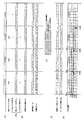
図8は、順序・位置信号生成部32の詳細な動作を説明するための図である。ここでは、演算要素データ「A」、「B」、「C」、「D」、「E」、「F」、「G」、「H」の順に、ベクトルレジスタ8に格納する場合が示される。図8(A)には、バンク6_1〜6_4に分散して8個の演算要素データ「A」〜「H」が格納される例が示される。また、図8(A)には、演算要素データ「A」〜「H」を含む要素データ列R1〜R4の読み出しアドレスが示される。ここでは、図面の右から左へ、かつ、上から下へアドレスが昇順に変化する。バンク6_1〜6_4ごとの読出しアドレスの順序は、読み出される要素データ列R1〜R4に含まれる演算要素データ「A」〜「H」のベクトルレジスタ8における格納順序、つまり、演算パイプライン12_3、12_4による処理順序に対応する。たとえば、アドレス順に示すと、バンク6_4には、アドレス「0x30」に、演算要素データ「A」を含む要素データ列R4が格納される。また、バンク6_1には、アドレス「0x40」に、演算要素データ「B」及び「C」を含む要素データ列R1が格納される。また、バンク6_2には、アドレス「0x50」に、演算要素データ「D」、「E」、及び「F」を含む要素データ列R2が格納される。そして、バンク6_3には、アドレス「0x60」に、演算要素データ「G」及び「H」を含む要素データ列R3が格納される。
FIG. 8 is a diagram for explaining the detailed operation of the order / position
図8(B)には、アドレス生成部30が生成するバンク6_1〜6_4ごとの読み出しアドレスrADDが示される。たとえば、バンク6_1については、読出しアドレス「0x40」が生成される。また、バンク6_2については、読出しアドレス「0x50」が生成される。また、バンク6_3については、読出しアドレス「0x60」が生成される。そして、バンク6_4については、読出しアドレス「0x30」が生成される。
FIG. 8B shows the read address rADD for each of the banks 6_1 to 6_4 generated by the
また、図8(B)には、アドレス生成部30が生成する各種処理信号PSが示される。各種処理信号PSは、バンクイネーブル信号BE、要素イネーブル信号EE、バンクオフセット信号BOである。バンクイネーブル信号BE、要素イネーブル信号EE、バンクオフセット信号BOは、読出しアドレスrADDに基づいて生成される。
FIG. 8B shows various processing signals PS generated by the
バンクイネーブル信号BEは、バンク6_1〜6_4ごとの読出しアドレスrADDの有効性を示す。バンクイネーブル信号BEは、たとえば1ビットの信号である。読出しアドレスrADDが生成された場合には、バンクイネーブル信号BEは有効性を示す値「1」となる。一方、読出しアドレスrADDが生成されない場合には、バンクイネーブル信号BEは値「0」となる。ここでは、バンク6_1〜6_4のすべてにおいて読出しアドレスrADDが生成されている。よって、バンク6_1〜6_4のすべてについて、読出しアドレスrADDの有効性を示す値「1」を有するバンクイネーブル信号BEが生成される。 The bank enable signal BE indicates the validity of the read address rADD for each of the banks 6_1 to 6_4. The bank enable signal BE is a 1-bit signal, for example. When the read address rADD is generated, the bank enable signal BE has a value “1” indicating validity. On the other hand, when the read address rADD is not generated, the bank enable signal BE has the value “0”. Here, the read address rADD is generated in all of the banks 6_1 to 6_4. Therefore, the bank enable signal BE having the value “1” indicating the validity of the read address rADD is generated for all of the banks 6_1 to 6_4.
要素イネーブル信号EEは、要素データ列R1〜R4における選択すべき演算要素データの位置を示す。要素データ列R1〜R4は、それぞれ8個の要素データを含む。よって、要素イネーブル信号は、各要素データ列R1〜R4について、たとえば8ビットの信号である。ここで、図面の右側から左側に列をカウントすると、たとえば、要素データ列R1には、1列目と2列目にそれぞれ演算要素データ「B」、「C」が含まれる。よって要素データ列R1に対応する要素イネーブル信号EEの値は、1列目から8列目まで順に、「1、1、0、0、0、0、0、0」となる。また、要素データ列R2には、2列目から4列目に演算要素データ「D」、「E」、及び「F」が含まれる。よって要素データ列R2に対応する要素イネーブル信号EEの値は、1列目から8列目まで順に、「0、1、1、1、0、0、0、0」となる。また、要素データ列R3には、4列目及び5列目に演算要素データ「G」及び「H」が含まれる。よって要素データ列R3に対応する要素イネーブル信号の値は、1列目から8列目まで順に、「0、0、0、1、1、0、0、0」となる。そして、要素データ列R4には、8列目に演算要素データ「A」が含まれる。よって要素データ列R4に対応する要素イネーブル信号EEの値は、1列目から8列目まで、順に「0、0、0、0、0、0、0、1」となる。 The element enable signal EE indicates the position of calculation element data to be selected in the element data strings R1 to R4. Each of the element data strings R1 to R4 includes eight element data. Therefore, the element enable signal is, for example, an 8-bit signal for each of the element data strings R1 to R4. Here, when counting the columns from the right side to the left side of the drawing, for example, the element data column R1 includes calculation element data “B” and “C” in the first column and the second column, respectively. Therefore, the value of the element enable signal EE corresponding to the element data string R1 is “1, 1, 0, 0, 0, 0, 0, 0” in order from the first column to the eighth column. In addition, the element data string R2 includes operation element data “D”, “E”, and “F” in the second to fourth columns. Therefore, the value of the element enable signal EE corresponding to the element data string R2 is “0, 1, 1, 1, 0, 0, 0, 0” in order from the first column to the eighth column. In addition, the element data string R3 includes calculation element data “G” and “H” in the fourth and fifth columns. Therefore, the value of the element enable signal corresponding to the element data string R3 is “0, 0, 0, 1, 1, 0, 0, 0” in order from the first column to the eighth column. The element data string R4 includes the calculation element data “A” in the eighth column. Therefore, the value of the element enable signal EE corresponding to the element data string R4 is “0, 0, 0, 0, 0, 0, 0, 1” in order from the first column to the eighth column.
バンクオフセット信号BOは、要素データ列R1〜R4に含まれる演算要素データの処理順序に対応する、バンク6_1〜6_4の順序を示す。バンクオフセット信号OSの値は、各バンク6_1〜6_4の読出しアドレスrADDの順序と、要素イネーブル信号EEの積算値から、次のように求められる。 The bank offset signal BO indicates the order of the banks 6_1 to 6_4 corresponding to the processing order of the calculation element data included in the element data strings R1 to R4. The value of the bank offset signal OS is obtained from the order of the read addresses rADD of the banks 6_1 to 6_4 and the integrated value of the element enable signal EE as follows.
まず、バンク6_1〜6_4ごとの読出しアドレスrADDの順序は、小さい方から次のような順序になる。
<1番目>バンク6_4の読出しアドレスrADD(「0x30」)
<2番目>バンク6_1の読出しアドレスrADD(「0x40」)
<3番目>バンク6_2の読出しアドレスrADD(「0x50」)
<4番目>バンク6_3の読出しアドレスrADD(「0x60」)
また、上記順序の各バンクの要素イネーブル信号EEの積算値は、次のようになる。
<1番目>バンク6_4の要素イネーブル信号EEの積算値「1」
<2番目>バンク6_1の要素イネーブル信号EEの積算値「2」
<3番目>バンク6_2の要素イネーブル信号EEの積算値「3」
<4番目>バンク6_3の要素イネーブル信号EEの積算値「2」
そして、各バンクのバンクオフセット信号BOの値は、1つ前の順番のバンクの、バンクオフセット信号BOの値とイネーブル信号EEの積算値の和として求められる。たとえば、次のとおりである。
<1番目>バンク6_4のバンクオフセット信号BO=「0」
<2番目>バンク6_1のバンクオフセット信号BO
=バンク6_4のバンクオフセット信号BO「0」+
バンク6_4の要素イネーブル信号EEの積算値「1」
=「1」
<3番目>バンク6_2のバンクオフセット信号BO
=バンク6_1のバンクオフセット信号BO「1」+
バンク6_1の要素イネーブル信号EEの積算値「2」
=「3」
<4番目>バンク6_3のバンクオフセット信号BO
=バンク6_2のバンクオフセット信号BO「3」+
バンク6_2の要素イネーブル信号EEの積算値「3」
=「6」
図8(C)には、順序・位置信号生成部32が生成する、バンク6_1〜6_4ごとの要素オフセット信号EO、順序信号S6、位置信号S4が示される。
First, the order of the read addresses rADD for each of the banks 6_1 to 6_4 is as follows from the smallest.
<First> Read address rADD (“0x30”) of bank 6_4
<Second> Read address rADD (“0x40”) of bank 6_1
<Third> Bank 6_2 read address rADD ("0x50")
<Fourth> Read address rADD (“0x60”) of bank 6_3
The integrated value of the element enable signal EE of each bank in the above order is as follows.
<First> Integrated value “1” of element enable signal EE of bank 6_4
<Second> Integrated value “2” of the element enable signal EE of the bank 6_1
<Third> Integrated value “3” of element enable signal EE of bank 6_2
<Fourth> Integrated value “2” of element enable signal EE of bank 6_3
Then, the value of the bank offset signal BO of each bank is obtained as the sum of the bank offset signal BO value and the integrated value of the enable signal EE of the bank in the previous order. For example:
<First> Bank offset signal BO = “0” of bank 6_4
<Second> Bank offset signal BO of bank 6_1
= Bank offset signal BO “0” of bank 6_4 +
Integrated value “1” of element enable signal EE of bank 6_4
= "1"
<Third> Bank offset signal BO of bank 6_2
= Bank offset signal BO “1” of bank 6_1 +
Integrated value “2” of element enable signal EE of bank 6_1
= "3"
<4th> Bank offset signal BO of bank 6_3
= Bank offset signal BO “3” of bank 6_2 +
Integrated value “3” of element enable signal EE of bank 6_2
= "6"
FIG. 8C shows the element offset signal EO, the order signal S6, and the position signal S4 for each of the banks 6_1 to 6_4, which are generated by the order / position
要素オフセット信号EOは、要素データ列R1〜R4ごとの、選択すべき演算要素データの順序を示す。要素オフセット信号EOの値は、バンク6_1〜6_4ごとの要素イネーブル信号EEの値を、アドレス順に積算して求められる。具体的には、次のとおりである。
<バンク6_1>
演算要素データ「B」の要素オフセット信号EO
=演算要素データ「B」の要素イネーブル信号EE「1」
演算要素データ「C」の要素オフセット信号EO
=演算要素データ「B」の要素オフセット信号EO「1」
+演算要素データ「C」の要素イネーブル信号EE「1」
=「2」
<バンク6_2>
演算要素データ「D」の要素オフセット信号EO
=演算要素データ「D」の要素イネーブル信号EE「1」
演算要素データ「E」の要素オフセット信号EO
=演算要素データ「D」の要素オフセット信号EO「1」
+演算要素データ「E」の要素イネーブル信号EE「1」
=「2」
演算要素データ「F」の要素オフセット信号EO
=演算要素データ「E」の要素オフセット信号EO「2」
+演算要素データ「F」の要素イネーブル信号EE「1」
=「3」
<バンク6_3>
演算要素データ「G」の要素オフセット信号EO
=演算要素データ「G」の要素イネーブル信号EE「1」
演算要素データ「H」の要素オフセット信号EO
=演算要素データ「G」の要素オフセット信号EO「1」
+演算要素データ「H」の要素イネーブル信号EE「1」
=「2」
<バンク6_4>
演算要素データ「A」の要素オフセット信号EO
=演算要素データ「A」の要素イネーブル信号EE「1」
次に、順序信号S6は、ベクトルレジスタ8における演算要素データの格納位置を示す。順序信号S6の値は、演算要素データが対応するバンクのバンクオフセット信号BOの値と、演算要素データの要素オフセット信号EOの値の和として求められる。具体的には、次のとおりである。
<バンク6_1>
演算要素データ「B」の順序信号S6
=バンク6_1のバンクオフセット信号BO「1」
+演算要素データ「B」の要素オフセット信号EO「1」
=「2」
演算要素データ「C」の順序信号S6
=バンク6_1のバンクオフセット信号BO「1」
+演算要素データ「C」の要素オフセット信号EO「2」
=「3」
<バンク6_2>
演算要素データ「D」の順序信号S6
=バンク6_2のバンクオフセット信号BO「3」
+演算要素データ「D」の要素オフセット信号EO「1」
=「4」
演算要素データ「E」の順序信号S6
=バンク6_2のバンクオフセット信号BO「3」
+演算要素データ「E」の要素オフセット信号EO「2」
=「5」
演算要素データ「F」の順序信号S6
=バンク6_2のバンクオフセット信号BO「3」
+演算要素データ「D」の要素オフセット信号EO「3」
=「6」
<バンク6_3>
演算要素データ「G」の順序信号S6
=バンク6_3のバンクオフセット信号BO「6」
+演算要素データ「D」の要素オフセット信号EO「1」
=「7」
演算要素データ「H」の順序信号S6
=バンク6_2のバンクオフセット信号BO「6」
+演算要素データ「E」の要素オフセット信号EO「2」
=「8」
<バンク6_4>
演算要素データ「A」の順序信号S6
=バンク6_3のバンクオフセット信号BO「0」
+演算要素データ「D」の要素オフセット信号EO「1」
=「1」
ここにおいて、演算要素データ「A」、「B」、「C」、「D」、「E」、「F」、「G」、「H」に、ベクトルレジスタ8に格納される順序「1」、「2」、「3」、「4」、「5」、「6」、「7」、「8」がそれぞれ対応付けられる。
The element offset signal EO indicates the order of calculation element data to be selected for each of the element data strings R1 to R4. The value of the element offset signal EO is obtained by integrating the values of the element enable signals EE for the banks 6_1 to 6_4 in the order of addresses. Specifically, it is as follows.
<Bank 6_1>
Element offset signal EO of calculation element data “B”
= Element enable signal EE “1” of operation element data “B”
Element offset signal EO of calculation element data “C”
= Element offset signal EO “1” of calculation element data “B”
+ Element enable signal EE “1” for operation element data “C”
= "2"
<Bank 6_2>
Element offset signal EO of calculation element data “D”
= Element enable signal EE “1” of operation element data “D”
Element offset signal EO of calculation element data “E”
= Element offset signal EO “1” of calculation element data “D”
+ Element enable signal EE “1” for operation element data “E”
= "2"
Element offset signal EO of calculation element data “F”
= Element offset signal EO “2” of operation element data “E”
+ Element enable signal EE “1” for operation element data “F”
= "3"
<Bank 6_3>
Element offset signal EO of calculation element data “G”
= Element enable signal EE “1” of operation element data “G”
Element offset signal EO of calculation element data “H”
= Element offset signal EO “1” of calculation element data “G”
+ Element enable signal EE “1” for operation element data “H”
= "2"
<Bank 6_4>
Element offset signal EO of calculation element data “A”
= Element enable signal EE “1” of operation element data “A”
Next, the order signal S6 indicates the storage position of the calculation element data in the
<Bank 6_1>
Order signal S6 of the calculation element data “B”
= Bank offset signal BO “1” of bank 6_1
+ Element offset signal EO “1” of operation element data “B”
= "2"
Order signal S6 of operation element data “C”
= Bank offset signal BO “1” of bank 6_1
+ Element offset signal EO “2” of calculation element data “C”
= "3"
<Bank 6_2>
Order signal S6 of the calculation element data “D”
= Bank offset signal BO “3” of bank 6_2
+ Element offset signal EO “1” of operation element data “D”
= "4"
Order signal S6 of the calculation element data “E”
= Bank offset signal BO “3” of bank 6_2
+ Element offset signal EO “2” of operation element data “E”
= "5"
Order signal S6 of the calculation element data “F”
= Bank offset signal BO “3” of bank 6_2
+ Element offset signal EO “3” of operation element data “D”
= "6"
<Bank 6_3>
Order signal S6 of the calculation element data “G”
= Bank offset signal BO “6” of bank 6_3
+ Element offset signal EO “1” of operation element data “D”
= "7"
Order signal S6 of operation element data “H”
= Bank offset signal BO “6” of bank 6_2
+ Element offset signal EO “2” of operation element data “E”
= "8"
<Bank 6_4>
Sequence signal S6 of the calculation element data “A”
= Bank offset signal BO “0” of bank 6_3
+ Element offset signal EO “1” of operation element data “D”
= "1"
Here, the operation element data “A”, “B”, “C”, “D”, “E”, “F”, “G”, “H” are stored in the
位置信号S4は、データ要素列R1〜R4に含まれる32個の要素データにおける、演算要素データ「A」〜「H」の位置を示す。たとえば、32個の要素データが要素データ列R1、R2、R3、R4の順にアドレス順に並べられたとして、「0」〜「31」の値が昇順に割り当てられる。そして、順序信号S6が割り当てられた演算要素データ「A」〜「H」に対し、対応する位置信号S4「1」〜「32」のいずれかが割り当てられる。たとえば、次のとおりである。
<要素データ列R1>
演算要素データ「B」:順序信号「2」、位置信号「0」
演算要素データ「C」:順序信号「3」、位置信号「1」
<要素データ列R2>
演算要素データ「D」:順序信号「4」、位置信号「9」
演算要素データ「E」:順序信号「5」、位置信号「10」
演算要素データ「F」:順序信号「6」、位置信号「11」
<要素データ列R3>
演算要素データ「G」:順序信号「7」、位置信号「19」
演算要素データ「H」:順序信号「8」、位置信号「20」
<要素データ列R4>
演算要素データ「A」:順序信号「1」、位置信号「31」
ここにおいて、演算要素データ「A」、「B」、「C」、「D」、「E」、「F」、「G」、「H」に、ベクトルレジスタ8に格納される順序「1」、「2」、「3」、「4」、「5」、「6」、「7」、「8」と、要素データR1、R2、R3、及びR4における位置とがそれぞれ対応付けられる。
The position signal S4 indicates the positions of the calculation element data “A” to “H” in the 32 element data included in the data element sequences R1 to R4. For example, assuming that 32 pieces of element data are arranged in the order of addresses in the order of element data strings R1, R2, R3, and R4, values “0” to “31” are assigned in ascending order. Then, any one of the corresponding position signals S4 “1” to “32” is assigned to the calculation element data “A” to “H” to which the order signal S6 is assigned. For example:
<Element data string R1>
Arithmetic element data “B”: sequence signal “2”, position signal “0”
Arithmetic element data “C”: sequence signal “3”, position signal “1”
<Element data string R2>
Arithmetic element data “D”: sequence signal “4”, position signal “9”
Arithmetic element data “E”: sequence signal “5”, position signal “10”
Arithmetic element data “F”: sequence signal “6”, position signal “11”
<Element data string R3>
Arithmetic element data “G”: sequence signal “7”, position signal “19”
Arithmetic element data “H”: sequence signal “8”, position signal “20”
<Element data string R4>
Arithmetic element data “A”: sequence signal “1”, position signal “31”
Here, the operation element data “A”, “B”, “C”, “D”, “E”, “F”, “G”, “H” are stored in the
次に、図7、図8を参照して、セレクタ部34の動作について説明する。セレクタ部34は、要素データ列R1〜R4から位置信号S4に基づいて演算要素データを選択し、選択した要素データを順序信号S6が示す格納順序でベクトルレジスタ8に格納する。具体的には、次のとおりである。セレクタ34_1〜34_8には、それぞれベクトルレジスタ8の格納順序「1」〜「8」の格納位置に対応する。そして、セレクタ34_1〜34_8は、それぞれ要素データ列R1〜R4の32個の要素データが入力される。そして、セレクタ34_1〜34_8は、位置信号S4と順序信号S6とに基づいて、32個の要素データから自らが対応する格納位置に格納すべき演算要素データを選択し、ベクトルレジスタ8に格納する。たとえば、セレクタ34_1〜34_8が対応する格納順序、順序信号S6の値、位置信号S4の値、及び格納する要素データの対応は、次のとおりである。
セレクタ34_1:格納順序「1」、順序信号「1」、位置信号「31」、演算要素データ「A」
セレクタ34_2:格納順序「2」、順序信号「2」、位置信号「0」、演算要素データ「B」
セレクタ34_3:格納順序「3」、順序信号「3」、位置信号「1」、演算要素データ「C」
セレクタ34_4:格納順序「4」、順序信号「4」、位置信号「9」、演算要素データ「D」
セレクタ34_5:格納順序「5」、順序信号「5」、位置信号「10」、演算要素データ「E」
セレクタ34_6:格納順序「6」、順序信号「6」、位置信号「11」、演算要素データ「F」
セレクタ34_7:格納順序「7」、順序信号「7」、位置信号「19」、演算要素データ「G」
セレクタ34_8:格納順序「8」、順序信号「8」、位置信号「20」、演算要素データ「H」
このようにして、バンク6_1〜6_4から読み出された要素データ列R1〜R4から、演算要素データ「A」〜「H」が選択される。そして、図8(D)に示すように、演算要素データ「A」〜「H」がベクトルレジスタ8に格納順序に従って格納される。
Next, the operation of the
Selector 34_1: storage order “1”, order signal “1”, position signal “31”, calculation element data “A”
Selector 34_2: storage order “2”, order signal “2”, position signal “0”, operation element data “B”
Selector 34_3: storage order “3”, order signal “3”, position signal “1”, calculation element data “C”
Selector 34_4: storage order “4”, order signal “4”, position signal “9”, calculation element data “D”
Selector 34_5: storage order “5”, order signal “5”, position signal “10”, operation element data “E”
Selector 34_6: storage order “6”, order signal “6”, position signal “11”, calculation element data “F”
Selector 34_7: storage order “7”, order signal “7”, position signal “19”, calculation element data “G”
Selector 34_8: storage order “8”, order signal “8”, position signal “20”, calculation element data “H”
Thus, the calculation element data “A” to “H” are selected from the element data strings R1 to R4 read from the banks 6_1 to 6_4. Then, as shown in FIG. 8D, the calculation element data “A” to “H” are stored in the
本実施形態によれば、バンク6_1〜6_4からは、32個の要素データを含む要素データ列R1〜R4が1回のアクセスで読み出されるので、レイテンシが抑制される。一方で、上述のような方法により、要素データ列R1〜R4の32個の要素データから、ベクトルレジスタ8に格納すべき8個の演算要素データが選択されて、処理順序でベクトルレジスタに格納される。よって、演算パイプライン12_3、12_4では、連続して要素データを処理できるので、良好なスループットを得ることができる。
According to the present embodiment, since the element data strings R1 to R4 including 32 element data are read from the banks 6_1 to 6_4 by one access, the latency is suppressed. On the other hand, eight arithmetic element data to be stored in the
なお、順序・位置信号生成部32は、アドレス生成部30から送られるバンクイネーブル信号BEをセレクタ部34に転送することが可能である。そうすることで、セレクタ部34は、バンクイネーブル信号BEが生成されたバンクから要素データ列が読み出されると、読み出された要素データ列から演算要素データを選択する。その一方、バンクイネーブル信号BEが生成されないバンクからは要素データ列が読み出されないので、要素データ列から演算要素データを選択する動作を実行しないようにする。
The order / position
図9は、読出しアドレスの有効性を示すバンクイネーブル信号BEが生成されない例を示す。図9(A)〜(C)では、図8(A)〜(C)で示した各種信号が示される。 FIG. 9 shows an example in which the bank enable signal BE indicating the validity of the read address is not generated. 9A to 9C show various signals shown in FIGS. 8A to 8C.
この例では、図9(A)に示すように、バンク6_2〜6_4に分散して8個の演算要素データ「A」〜「H」が格納される。たとえば、アドレス順に示すと、バンク6_3には、アドレス「0x60」に、演算要素データ「A」及び「B」を含む要素データ列R3が格納される。また、バンク6_4には、アドレス「0x70」に、演算要素データ「C」、「D」、及び「E」を含む要素データ列R4が格納される。また、バンク6_2には、アドレス「0x90」に、演算要素データ「F」、「G」、及び「H」を含む要素データ列R2が格納される。そして、ここでは、バンク6_1には、演算要素データが格納されない。 In this example, as shown in FIG. 9A, eight calculation element data “A” to “H” are stored in the banks 6_2 to 6_4 in a distributed manner. For example, in the order of addresses, the bank 6_3 stores the element data string R3 including the calculation element data “A” and “B” at the address “0x60”. The bank 6_4 stores an element data string R4 including the calculation element data “C”, “D”, and “E” at the address “0x70”. The bank 6_2 stores an element data string R2 including the calculation element data “F”, “G”, and “H” at the address “0x90”. Here, the calculation element data is not stored in the bank 6_1.
よって、図9(B)に示すように、アドレス生成部30により、バンク6_3については、読出しアドレス「0x60」が生成される。また、バンク6_4については、読出しアドレス「0x70」が生成される。また、バンク6_2については、読出しアドレス「0x90」が生成される。そして、バンク6_1については、読出しアドレスが生成されない。よって、バンク6_2〜6_4からは要素データ列R2〜R4が読み出され、バンク6_1からは要素データ列R1が読み出されない。
Therefore, as shown in FIG. 9B, the
ここで、読出しアドレスrADDが生成されるバンク6_2〜4についてのバンクイネーブル信号BEは、有効を示す値「1」を有する。しかし一方で、読出しアドレスrADDが生成されないバンク6_1についてのバンクイネーブル信号BEは、無効を示す値「0」となる。つまり、読出しアドレスrADDの有効性を示すバンクイネーブル信号BEが生成されない。このようなバンクイネーブル信号BEが転送されることにより、セレクタ部34は次のように動作する。なお、図9(B)の要素イネーブル信号EE、バンクオフセット信号BOは、図8(B)で示した方法と同様にして求められ、図9(C)の要素オフセット信号EO、順序信号S6、及び位置信号S4は、図8(C)で示した方法と同様にして求められる。
Here, the bank enable signal BE for the banks 6_2 to 4-4 where the read address rADD is generated has a value “1” indicating validity. However, on the other hand, the bank enable signal BE for the bank 6_1 in which the read address rADD is not generated has a value “0” indicating invalidity. That is, the bank enable signal BE indicating the validity of the read address rADD is not generated. When such a bank enable signal BE is transferred, the
セレクタ部34のセレクタ34_1〜34_8は、それぞれ要素データ列R2〜R4の24個の要素データが入力されたとき、バンクイネーブル信号BEが生成されたバンク6_2〜4に対応する要素データ列R2〜3に対し、要素データを選択する処理を行う。その一方、セレクタ部34のセレクタ34_1〜34_8は、バンクイネーブル信号BEが生成されないバンク6_1に対応する要素データ列R1が入力されないので、要素データ列R1に対して行うはずであった演算要素データを選択する処理を行わない。そうすることで、電力の無駄な消費や処理負荷を軽減することができる。
The selectors 34_1 to 34_8 of the
そして、上記の処理の結果、図9(D)に示すように、演算要素データ「A」〜「H」がベクトルレジスタ8に格納順序に従って格納される。
As a result of the above processing, the operation element data “A” to “H” are stored in the
[ベクトルレジスタ8から演算要素データを読み出してデータメモリ6に書き込む場合]
図10は、ベクトルレジスタ8から演算要素データを読み出してデータメモリ6に書き込むためのメモリ制御装置の構成を示す。メモリ制御装置は、要素データ列R1〜R4を書き込むためのバンク6_1〜6_4ごとの書込みアドレスwADDを生成するアドレス生成部30を有する。アドレス生成部30は、たとえばロード・ストアパイプライン12_1、12_2内のモジュールである。アドレス生成部30は、命令デコーダ4から入力されるアドレス生成用データ4aに基づいて、書込みアドレスwADDを生成する。アドレス生成部30は、たとえば、シーケンシャルアクセスの場合の書込みアドレスwADDを生成するシーケンシャルアドレス生成部30_1、インダイレクトアクセスの場合の書込みアドレスwADDを生成するインダイレクトアドレス生成部30_2、及びストライドアクセスの場合の書込みアドレスwADDを生成するストライドアドレス生成部30_3を有する。アドレス生成部30が生成したバンク6_1〜6_4ごとの書込みアドレスwADDは、たとえばレジスタ40に一旦格納されてから、データメモリ6のバンク6_1〜6_4にそれぞれ入力される。その一方、アドレス生成部30では、たとえば、シーケンシャルアドレス生成部30_1、インダイレクトアドレス生成部30_2、及びストライドアドレス生成部30_3により、各種処理信号PSが生成される。そして、バンク6_1〜6_4ごとの書込みアドレスwADDと各種処理信号PSは、レジスタ31に格納される。
[When arithmetic element data is read from the
FIG. 10 shows a configuration of a memory control device for reading operation element data from the
メモリ制御装置は、演算パイプライン12_3、12_4による処理順序でベクトルレジスタ8に格納された、データメモリ6に書き込むべき演算要素データのベクトルレジスタ8における格納順序を示す順序信号S5と、バンク6_1〜6_4にそれぞれ書き込まれる要素データ列R1〜R4に書き込むべき要素データを挿入する位置を示す位置信号S7とを生成する順序・位置信号生成部32を有する。順序・位置信号生成部32は、たとえば、マルチプレクサ14内のモジュールである。順序・位置信号生成部32は、レジスタ31に格納された書込みアドレスwADDと各種処理信号PSとを読み出し、これらに基づいて位置信号S7と順序信号S5とを生成する。その詳細については後述する。
The memory control device includes an order signal S5 indicating the storage order in the
また、メモリ制御装置は、バンク6_1〜6_4に書き込まれる要素データ列R1〜R4における位置信号S7が示す位置に、順序信号S5が示す順序で書き込むべき要素データを挿入するセレクタ部35を有する。セレクタ部35は、たとえば、マルチプレクサ14に含まれる。セレクタ部35は、たとえば、要素データ列R1〜R4に含まれる32個の要素データごとのセレクタ35_1〜35_32を有する。セレクタ35_1〜35_32には、それぞれ、ベクトルレジスタ8から読み出される8個の演算要素データ8aが入力される。演算要素データ8aは、たとえばレジスタ44に一旦格納されてから、セレクタ35_1〜35_32に入力される。そして、セレクタ35_1〜35_32は、位置信号S7と順序信号S5とに基づいて、8個の演算要素データ8aから自らが対応する位置に挿入すべき演算要素データを選択し、要素データ列R1〜R4に挿入する。
In addition, the memory control device includes a
さらに、セレクタ部35は、たとえば命令デコーダ4からデータマスク信号DMが入力される。データマスク信号DMは、演算要素データのデータメモリ6への書込みの許可・不許可を示す。データマスク信号DMは、たとえば8ビットの信号である。各ビットは、8個の要素データ8aの書込み許可・不許可を示す。データマスク信号DMは、たとえばレジスタ42に一旦格納されてから、セレクタ部35に入力される。
Furthermore, the
セレクタ部35は、データマスク信号DMに基づいて、32ビットのデータマスク信号DM2を生成する。データマスク信号DM2は、バンク6_1〜6_4に、要素データ列R1〜R4の書き込みの許可・不許可を指示するための信号である。各ビットは、要素データ列R1〜R4に含まれる32個の要素データに対応する。セレクタ部35は、データマスク信号DM2を生成する32個のセレクタ36_1〜36_32を有する。セレクタ36_1〜36_32は、それぞれ要素データ列R1〜R4に含まれる32個の要素データに対応する。セレクタ36_1〜36_32には、それぞれ8ビットのデータマスク信号DMが入力される。そして、セレクタ36_1〜36_32は、位置信号S7と順序信号S5とに基づいて、自らが対応する位置への要素データの挿入許可・不許可を示す値(「1」または「0」)を生成する。このようにして8ビットのデータマスク信号DM2が生成される。データマスク信号DM2は、バンク6_1〜6_4に入力される。
The
データメモリ6では、バンク6_1〜6_4が、それぞれ要素データ列R1〜R4を書込みアドレスwADDに書き込む。その際、データマスク信号DM2により許可された要素データのみが書き込まれる。データマスク信号DM2を用いることで、データメモリ6においてデータが破壊されたり不整合が生じたりすることを防止できる。
In the
図11は、順序・位置所信号生成部32の詳細な動作を説明するための図である。図11(A)には、アドレス生成部30が生成するバンク6_1〜6_4ごとの書込みアドレスwADDが示される。たとえば、バンク6_1については、書込みアドレス「0x40」が生成される。また、バンク6_2については、書込みアドレス「0x50」が生成される。また、バンク6_3については、書込みアドレス「0x60」が生成される。そして、バンク6_4については、書込みアドレス「0x30」が生成される。
FIG. 11 is a diagram for explaining the detailed operation of the order / position
上記書込みアドレスwADDは、バンク6_1〜6_4に、図11(E)に示すように要素データ列R1〜R4を書き込むための書込みアドレスwADDである。要素データ列R1〜R4には、8個の演算要素データ「A」、「B」、「C」、「D」、「E」、「F」、「G」、「H」が含まれる。ここでは、図面の右から左へ、かつ、上から下へアドレスが昇順に変化する。バンク6_1〜6_4に書き込まれる演算要素データ「A」〜「H」のアドレス順は、ベクトルレジスタ8における格納順、つまり、演算パイプライン12_3、12_4による処理順序に対応する。
The write address wADD is a write address wADD for writing the element data strings R1 to R4 to the banks 6_1 to 6_4 as shown in FIG. The element data strings R1 to R4 include eight pieces of calculation element data “A”, “B”, “C”, “D”, “E”, “F”, “G”, and “H”. Here, the addresses change in ascending order from right to left and from top to bottom in the drawing. The address order of the operation element data “A” to “H” written in the banks 6_1 to 6_4 corresponds to the storage order in the
また、図11(A)には、アドレス生成部30が生成する各種処理信号PSが示される。各種処理信号PSは、バンクイネーブル信号BE、要素イネーブル信号EE、バンクオフセット信号BOである。バンクイネーブル信号BE、要素イネーブル信号EE、バンクオフセット信号BOは、書込みアドレスwADDに基づいて生成される。
FIG. 11A shows various processing signals PS generated by the
バンクイネーブル信号BEは、バンク6_1〜6_4ごとの書込みアドレスwADDの有効性を示す。バンクイネーブル信号BEは、たとえば1ビットの信号である。書込みアドレスwADDが生成された場合には、バンクイネーブル信号BEは有効性を示す値「1」となる。一方、書込みアドレスrADDが生成されない場合には、バンクイネーブル信号BEは値「0」となる。ここでは、バンク6_1〜6_4のすべてにおいて書込みアドレスwADDが生成されている。よって、バンク6_1〜6_4のすべてについて、書込みアドレスwADDの有効性を示す値「1」を有するバンクイネーブル信号BEが生成される。 The bank enable signal BE indicates the validity of the write address wADD for each of the banks 6_1 to 6_4. The bank enable signal BE is a 1-bit signal, for example. When the write address wADD is generated, the bank enable signal BE has a value “1” indicating validity. On the other hand, when the write address rADD is not generated, the bank enable signal BE has the value “0”. Here, the write address wADD is generated in all of the banks 6_1 to 6_4. Therefore, the bank enable signal BE having the value “1” indicating the validity of the write address wADD is generated for all of the banks 6_1 to 6_4.
要素イネーブル信号EEは、要素データ列R1〜R4に挿入すべき演算要素データの位置を示す。たとえば、図11(D)に示すように、要素データ列R1には、1列目と2列目にそれぞれ演算要素データ「B」、「C」が挿入される。よって、要素イネーブル信号EEの値は、1列目から8列目まで順に、「1、1、0、0、0、0、0、0」となる。また、要素データ列R2には、2列目から4列目に演算要素データ「D」、「E」、及び「F」が挿入される。よって要素データ列R2に対応する要素イネーブル信号EEの値は、1列目から8列目まで順に、「0、1、1、1、0、0、0、0」となる。また、要素データ列R3には、4列目及び5列目に演算要素データ「G」及び「H」が挿入される。よって要素データ列R3に対応する要素イネーブル信号の値は、1列目から8列目まで順に、「0、0、0、1、1、0、0、0」となる。そして、要素データ列R4には、8列目に演算要素データ「A」が挿入される。よって要素データ列R4に対応する要素イネーブル信号EEの値は、1列目から8列目まで、順に「0、0、0、0、0、0、0、1」となる。 The element enable signal EE indicates the position of operation element data to be inserted into the element data strings R1 to R4. For example, as shown in FIG. 11D, operation element data “B” and “C” are inserted into the first column and the second column, respectively, in the element data column R1. Therefore, the value of the element enable signal EE is “1, 1, 0, 0, 0, 0, 0, 0” in order from the first column to the eighth column. In the element data string R2, calculation element data “D”, “E”, and “F” are inserted in the second to fourth columns. Therefore, the value of the element enable signal EE corresponding to the element data string R2 is “0, 1, 1, 1, 0, 0, 0, 0” in order from the first column to the eighth column. In the element data string R3, calculation element data “G” and “H” are inserted in the fourth and fifth columns. Therefore, the value of the element enable signal corresponding to the element data string R3 is “0, 0, 0, 1, 1, 0, 0, 0” in order from the first column to the eighth column. In the element data string R4, the calculation element data “A” is inserted in the eighth column. Therefore, the value of the element enable signal EE corresponding to the element data string R4 is “0, 0, 0, 0, 0, 0, 0, 1” in order from the first column to the eighth column.
バンクオフセット信号BOは、要素データ列R1〜R4に挿入すべき演算要素データの順序に対応する、バンク6_1〜6_4の順序を示す。バンクオフセット信号BOの値は、各バンク6_1〜6_4の読出しアドレスwADDの順序と、要素イネーブル信号EEの積算値から求められる。具体的な方法は、図8(B)で示したとおりである。 The bank offset signal BO indicates the order of the banks 6_1 to 6_4 corresponding to the order of the operation element data to be inserted into the element data strings R1 to R4. The value of the bank offset signal BO is obtained from the order of the read addresses wADD of the banks 6_1 to 6_4 and the integrated value of the element enable signal EE. A specific method is as shown in FIG.
図11(B)には、順序・位置信号生成部32が生成する、バンク6_1〜6_4ごとの要素オフセット信号EO、順序信号S5、位置信号S7が示される。要素オフセット信号EOは、要素データ列R1〜R4ごとの、挿入すべき演算要素データの順序を示す。要素オフセット信号EOの値は、バンク6_1〜6_4ごとの要素イネーブル信号EEの値を、アドレス順に積算して求められる。具体的な方法は、図8(C)に示したとおりである。
FIG. 11B shows an element offset signal EO, an order signal S5, and a position signal S7 for each of the banks 6_1 to 6_4, which are generated by the order / position
順序信号S5は、ベクトルレジスタ8における演算要素データの格納位置を示す。ベクトルレジスタ8における格納順序「1」〜「8」と演算要素データ「A」〜「H」の対応が、図11(C)に示される。なお、図11(C)には、各演算要素データの書込みの許可・不許可を規定するデータマスク信号DMが示される。順序信号S5の値は、演算要素データが対応するバンクのバンクオフセット信号BOの値と、演算要素データの要素オフセット信号EOの値の和として求められる。具体的な方法は、図8(C)で示したとおりである。
The order signal S5 indicates the storage position of the calculation element data in the
ここにおいて、演算要素データ「A」、「B」、「C」、「D」、「E」、「F」、「G」、「H」に、ベクトルレジスタ8に格納された順序「1」、「2」、「3」、「4」、「5」、「6」、「7」、「8」がそれぞれ対応付けられる。
Here, the operation element data “A”, “B”, “C”, “D”, “E”, “F”, “G”, “H” and the order “1” stored in the
位置信号S7は、データ要素列R1〜R4の32個の要素データにおける、演算要素データ「A」〜「H」を挿入すべき挿入位置を示す。たとえば、32個の要素データが要素データ列R1、R2、R3、R4の順にアドレス順に並べられ、「0」〜「31」の値が昇順に割り当てられる。そして、順序信号S5が割り当てられた演算要素データ「A」〜「H」に対し、対応する位置信号「1」〜「32」のいずれかが割り当てられる。たとえば、次のとおりである。
<要素データ列R1>
挿入すべき演算要素データ「B」:順序信号「2」、位置信号「0」
挿入すべき演算要素データ「C」:順序信号「3」、位置信号「1」
<要素データ列R2>
挿入すべき演算要素データ「D」:順序信号「4」、位置信号「9」
挿入すべき演算要素データ「E」:順序信号「5」、位置信号「10」
挿入すべき演算要素データ「F」:順序信号「6」、位置信号「11」
<要素データ列R3>
挿入すべき演算要素データ「G」:順序信号「7」、位置信号「19」
挿入すべき演算要素データ「H」:順序信号「8」、位置信号「20」
<要素データ列R4>
挿入すべき演算要素データ「A」:順序信号「1」、位置信号「31」
ここにおいて、演算要素データ「A」、「B」、「C」、「D」、「E」、「F」、「G」、「H」と、ベクトルレジスタ8に格納された順序「1」、「2」、「3」、「4」、「5」、「6」、「7」、「8」と、要素データR1、R2、R3、及びR4における挿入位置とがそれぞれ対応付けられる。
The position signal S7 indicates the insertion position where the calculation element data “A” to “H” should be inserted in the 32 element data of the data element sequences R1 to R4. For example, 32 element data are arranged in the order of addresses in the order of element data strings R1, R2, R3, and R4, and values “0” to “31” are assigned in ascending order. Then, any one of the corresponding position signals “1” to “32” is assigned to the calculation element data “A” to “H” to which the order signal S5 is assigned. For example:
<Element data string R1>
Calculation element data “B” to be inserted: sequence signal “2”, position signal “0”
Calculation element data “C” to be inserted: sequence signal “3”, position signal “1”
<Element data string R2>
Calculation element data “D” to be inserted: sequence signal “4”, position signal “9”
Operation element data “E” to be inserted: sequence signal “5”, position signal “10”
Calculation element data “F” to be inserted: sequence signal “6”, position signal “11”
<Element data string R3>
Calculation element data “G” to be inserted: sequence signal “7”, position signal “19”
Calculation element data “H” to be inserted: sequence signal “8”, position signal “20”
<Element data string R4>
Arithmetic element data “A” to be inserted: sequence signal “1”, position signal “31”
Here, the calculation element data “A”, “B”, “C”, “D”, “E”, “F”, “G”, “H”, and the order “1” stored in the
次に、図10、図11を参照して、セレクタ部35の動作について説明する。セレクタ部35は、複数のバンク6_1〜6_4に書き込まれる要素データ列R1〜R4における位置信号S5が示す位置に、順序信号S5が示す順序で書き込むべき要素データを挿入する。具体的には、次のとおりである。
Next, the operation of the
セレクタ35_1〜35_32は、それぞれ要素データ列R1〜R4における32個の要素データの位置「0」〜「31」に対応する。セレクタ35_1〜35_32は、ベクトルレジスタ8から読み出された8個の演算要素データ8a、つまり「A」〜「H」が入力される。そして、セレクタ35_1〜35_32は、位置信号S7と順序信号S5とに基づいて、8個の演算要素データ8aから自らが対応する挿入位置に挿入すべき演算要素データを選択し、要素データ列R1〜R4に挿入する。たとえば、セレクタ35_1〜35_32のうち、演算要素データ「A」〜「H」を挿入するセレクタの順序信号S5の値、位置信号S7の値、及び挿入する要素データの対応は、次のとおりである。
<セレクタ35_2> 順序信号「2」、位置信号「0」、演算要素データ「B」
<セレクタ35_3> 順序信号「3」、位置信号「1」、演算要素データ「C」
<セレクタ35_9> 順序信号「4」、位置信号「9」、演算要素データ「D」
<セレクタ35_10> 順序信号「5」、位置信号「10」、演算要素データ「E」
<セレクタ35_11> 順序信号「6」、位置信号「11」、演算要素データ「F」
<セレクタ35_19> 順序信号「7」、位置信号「19」、演算要素データ「G」
<セレクタ35_20> 順序信号「8」、位置信号「20」、演算要素データ「H」
<セレクタ35_31> 順序信号「1」、位置信号「31」、演算要素データ「A」
なお、上記以外のセレクタ35_1、35_4〜8、35_12〜18、35_21〜30は、順序信号「0」が対応し、したがって挿入すべき演算要素データが対応しないので、挿入を行わない。このようにして、ベクトルレジスタ8から読み出された演算要素データ「A」〜「H」が、要素データ列R1〜R4に挿入される。
The selectors 35_1 to 35_32 correspond to the positions “0” to “31” of the 32 element data in the element data strings R1 to R4, respectively. The
<Selector 35_2> Order signal “2”, position signal “0”, calculation element data “B”
<Selector 35_3> Order signal “3”, position signal “1”, calculation element data “C”
<Selector 35_9> Order signal “4”, position signal “9”, calculation element data “D”
<Selector 35_10> Order signal “5”, position signal “10”, calculation element data “E”
<Selector 35_11> Order signal “6”, position signal “11”, calculation element data “F”
<Selector 35_19> Order signal “7”, position signal “19”, calculation element data “G”
<Selector 35_20> Order signal “8”, position signal “20”, calculation element data “H”
<Selector 35_31> Order signal “1”, position signal “31”, calculation element data “A”
The selectors 35_1, 35_4 to 8, 35_12 to 18, 35_21 to 30 other than those described above are not inserted because the order signal “0” corresponds to the arithmetic element data to be inserted. In this way, the calculation element data “A” to “H” read from the
図11(D)には、演算要素データ「A」〜「H」が挿入されたデータ列R1〜R4が示される。また、図11(D)には、図11(C)のデータマスク信号DMから生成されたデータマスク信号DM2が示される。データマスク信号DM2は、32ビットの信号である。書込みが許可されるデータ要素に対応するビットの値が「0」、書込みが許可されないデータ要素に対応するビットの値が「1」である。ここでは、データ要素「B」、「D」、「F」の書込みが不許可の場合が示される。 FIG. 11D shows data strings R1 to R4 into which the calculation element data “A” to “H” are inserted. FIG. 11D shows a data mask signal DM2 generated from the data mask signal DM of FIG. The data mask signal DM2 is a 32-bit signal. The value of the bit corresponding to the data element for which writing is permitted is “0”, and the value of the bit corresponding to the data element for which writing is not permitted is “1”. Here, a case where writing of data elements “B”, “D”, and “F” is not permitted is shown.
上記のようにして演算要素データ「A」〜「H」が挿入された要素データ列R1〜R4が、図11(E)に示すように、バンク6_1〜6_4に1回のアクセスで書き込まれる。よって、レイテンシが抑制される。また、その際、要素データの書込みを許可・不許可できるので、データメモリ6のデータを保護できる。なお、図11(E)では、書込み不許可の演算要素データは「×」印が付されている。また、一方で、演算パイプライン12_3、12_4は、連続して要素データを処理して演算結果を出力できるので、パイプラインストールを低減できる。よって、良好なスループットを得ることができる。
The element data strings R1 to R4 into which the calculation element data “A” to “H” are inserted as described above are written to the banks 6_1 to 6_4 by one access as shown in FIG. Therefore, latency is suppressed. At this time, writing of element data can be permitted / denied, so that data in the
なお、順序・位置信号生成部32は、アドレス生成部30から送られるバンクイネーブル信号BEをセレクタ部35に転送することが可能である。セレクタ部35は、バンクイネーブル信号BEが生成されたバンクに書き込まれる要素データ列に、演算要素データを挿入する。その一方、セレクタ部35は、バンクイネーブル信号BEが生成されないバンクには要素データ列が書き込まれないので、演算要素データを挿入する処理を行わないようにする。
Note that the order / position
図12は、書込みアドレスの有効性を示すバンクイネーブル信号BEが生成されない例を示す。図12(A)〜(E)では、図11(A)〜(E)で示した各種信号が示される。 FIG. 12 shows an example in which the bank enable signal BE indicating the validity of the write address is not generated. 12A to 12E show various signals shown in FIGS. 11A to 11E.
この例では、図12(E)に示すように、バンク6_2〜4に分散して8個の演算要素データ「A」〜「H」が書き込まれる。たとえば、アドレス順に示すと、バンク6_3には、アドレス「0x60」に、演算要素データ「A」及び「B」を含む要素データ列R3が書き込まれる。また、バンク6_4には、アドレス「0x70」に、演算要素データ「C」、「D」、及び「E」を含む要素データ列R4が書き込まれる。また、また、バンク6_2には、アドレス「0x90」に、演算要素データ「F」、「G」、及び「H」を含む要素データ列R2が書き込まれる。そして、バンク6_1には、要素データが書き込まれない。 In this example, as shown in FIG. 12E, eight pieces of arithmetic element data “A” to “H” are written in a distributed manner in the banks 6_2 to 4_2. For example, in the order of addresses, the element data string R3 including the calculation element data “A” and “B” is written in the address “0x60” in the bank 6_3. In the bank 6_4, the element data string R4 including the calculation element data “C”, “D”, and “E” is written at the address “0x70”. In addition, in the bank 6_2, the element data string R2 including the calculation element data “F”, “G”, and “H” is written at the address “0x90”. Element data is not written in the bank 6_1.
よって、図12(A)に示すように、アドレス生成部30により、バンク6_2、6_3、及び6_4については、それぞれ書込みアドレス「0x90」、「0x60」、及び「0x70」が生成される。そして、バンク6_1については、書込みアドレスが生成されない。すると、書込みアドレスwADDが生成されるバンク6_2〜4についてのバンクイネーブル信号BEは、有効を示す値「1」を有する。しかし一方で、書込みアドレスwADDが生成されないバンク6_1についてのバンクイネーブル信号BEは、無効を示す値「0」となる。つまり、書込みアドレスwADDの有効性を示すバンクイネーブル信号BEが生成されない。
Therefore, as illustrated in FIG. 12A, the
このようなバンクイネーブル信号BEが転送されることにより、セレクタ部35は次のように動作する。なお、図12(A)の要素イネーブル信号EE、バンクオフセット信号BOは、図11(A)で示した方法と同様にして求められ、図12(B)の要素オフセット信号EO、順序信号S5、及び位置信号S7は、図11(B)で示した方法と同様にして求められる。
When such a bank enable signal BE is transferred, the
セレクタ部35のセレクタ35_1〜35_32は、それぞれ8個の演算要素データ「A」〜「H」が入力されたとき、バンクイネーブル信号BEが生成されたバンク6_2〜4に対応する要素データ列R2〜3に対しては、図12(B)に示す順序信号S5と位置信号S7とに基づいて要素データを挿入する処理を行う。しかしその一方、セレクタ35_1〜32は、バンクイネーブル信号BEが生成されないバンク6_1に対応する要素データ列R1に対しては要素データを挿入する処理を行わない。そうすることで、電力の無駄な消費や処理負荷を軽減することができる。
The selectors 35_1 to 35_32 of the
上記の結果、図12(C)で示すようにベクトルレジスタ8に格納された演算要素データが、図12(E)で示すようにデータメモリ6の各バンクに書き込まれる。また、その際、図12(C)で示すマスクデータ信号DMにより演算要素データの書き込みが許可または不許可される。
As a result, the calculation element data stored in the
上述したベクトルプロセッサ1は、たとえば、携帯通信端末に搭載され、ベースバンド信号を要素データとしてFFT(Fast Fourier Transforms)処理などを行う信号処理装置に適用される。あるいは、これに限定されず、たとえば画素データを要素データとして画像処理を行う画像処理装置などにも適用することができる。本実施形態によれば、データメモリの不連続なアドレスにアクセスして要素データを読み書きする場合であっても、最小限の回路構成により良好なスループットを得ることができる。
The
以上の実施の形態をまとめると、次の付記のとおりである。 The above embodiment is summarized as follows.
(付記1)
読出しアドレスの入力に応答して複数の要素データを有する要素データ列が読み出される複数のバンクを有するメモリから、前記要素データ列を読み出すためのバンクごとの前記読出しアドレスを生成する第1の生成部と、
前記要素データ列における選択すべき要素データの位置を示す位置信号と、前記選択すべき要素データをレジスタに格納する格納順序を示す順序信号とを生成する第2の生成部と、
前記複数のバンクからそれぞれ読み出された前記要素データ列から前記位置信号に基づいて前記選択すべき要素データを選択し、当該選択した要素データを前記順序信号が示す格納順序で前記レジスタに格納するセレクタ部とを有し、
前記レジスタに格納された要素データは、前記格納順序でベクトルプロセッサに処理される、メモリ制御装置。
(Appendix 1)
A first generation unit that generates the read address for each bank for reading the element data string from a memory having a plurality of banks from which an element data string having a plurality of element data is read in response to input of a read address When,
A second generation unit that generates a position signal indicating a position of element data to be selected in the element data string and an order signal indicating a storage order for storing the element data to be selected in a register;
The element data to be selected is selected based on the position signal from the element data strings read from the plurality of banks, and the selected element data is stored in the register in the storage order indicated by the order signal. And a selector unit,
The element control data stored in the register is processed by the vector processor in the storage order.
(付記2)
付記1において、
前記読出しアドレスの有効性を示すイネーブル信号をさらに生成し、
前記セレクタ部は、前記イネーブル信号が生成されたバンクから読み出される前記要素データ列から前記選択すべき要素データを選択し、前記イネーブル信号が生成されないバンクから読み出される前記要素データ列から前記選択すべき要素データを選択しないメモリ制御装置。
(Appendix 2)
In
Further generating an enable signal indicating the validity of the read address;
The selector unit selects the element data to be selected from the element data string read from the bank where the enable signal is generated, and should select the element data string read from the bank where the enable signal is not generated. A memory controller that does not select element data.
(付記3)
付記1または2において、
前記バンクごとの読出しアドレスの順序は、当該読出しアドレスにより読み出される前記要素データ列に含まれる前記選択すべき要素データの前記格納順に対応し、
前記第2の生成部は、前記バンクごとの読出しアドレスに基づいて生成される、前記複数のバンクから読み出される要素データ列の順序を示す第1のオフセット信号と、前記複数のバンクから読み出される要素データ列ごとの前記選択すべき要素データの順序を示す第2のオフセット信号とに基づいて前記順序信号を生成するメモリ制御装置。
(Appendix 3)
In
The order of the read address for each bank corresponds to the storage order of the element data to be selected included in the element data string read by the read address,
The second generation unit generates a first offset signal indicating an order of element data strings read from the plurality of banks, generated based on a read address for each bank, and an element read from the plurality of banks A memory control device for generating the order signal based on a second offset signal indicating the order of the element data to be selected for each data string.
(付記4)
複数の要素データを有する要素データ列が、入力された書込みアドレスに書き込まれる複数のバンクを有するメモリに、前記要素データ列を書き込むためのバンクごとの書込みアドレスを生成する第1の生成部と、
ベクトルプロセッサによる処理順序でレジスタに格納された、前記メモリに書き込むべき要素データの当該レジスタにおける格納順序を示す順序信号と、前記複数のバンクにそれぞれ書き込まれる要素データ列に前記書き込むべき要素データを挿入する位置を示す位置信号とを生成する第2の生成部と、
前記複数のバンクに書き込まれる要素データ列における前記位置信号が示す位置に、前記順序信号が示す順序で前記書き込むべき要素データを挿入するセレクタ部とを有し、
前記書き込むべき要素データ列が格納された要素データ列が、前記バンクごとの書込みアドレスに書き込まれる、メモリ制御装置。
(Appendix 4)
A first generation unit that generates a write address for each bank for writing the element data string in a memory having a plurality of banks in which the element data string having a plurality of element data is written to the input write address;
An order signal indicating the storage order of the element data to be written to the memory, stored in the register in the processing order by the vector processor, and the element data to be written are inserted into the element data strings respectively written to the plurality of banks. A second generation unit that generates a position signal indicating a position to perform,
A selector unit that inserts the element data to be written in the order indicated by the order signal at the position indicated by the position signal in the element data string written to the plurality of banks;
The memory control device, wherein the element data string storing the element data string to be written is written to a write address for each bank.
(付記5)
付記4において、
前記第1の生成部は、前記書込みアドレスの有効性を示すイネーブル信号をさらに生成し、
前記セレクタ部は、前記イネーブル信号が生成されたバンクに書き込まれる前記要素データ列に前記書き込むべき要素データを挿入し、前記イネーブル信号が生成されないバンクに書き込まれる前記要素データ列に前記書き込むべき要素データを挿入しないメモリ制御装置。
(Appendix 5)
In
The first generation unit further generates an enable signal indicating the validity of the write address,
The selector unit inserts the element data to be written into the element data string written in the bank where the enable signal is generated, and the element data to be written into the element data string written in the bank where the enable signal is not generated. Does not insert memory control device.
(付記6)
付記4または5において、
前記セレクタ部は、前記書き込むべき要素データの書込みの許可・不許可を示すマスク信号に基づいて、前記書込みが許可された前記書き込むべき要素データを前記複数のバンクに書き込まれる要素データ列に挿入し、前記書込みが不許可の前記書込むべき要素データを前記複数のバンクに書き込まれる要素データ列に挿入しない、メモリ制御装置。
(Appendix 6)
In
The selector unit inserts the element data to be written, which is permitted to be written, into the element data string to be written in the plurality of banks based on a mask signal indicating permission / non-permission of writing of the element data to be written. The memory control device does not insert the element data to be written, which is not permitted to be written, into the element data string to be written in the plurality of banks.
(付記7)
付記4乃至6のいずれかにおいて、
前記バンクごとの書込みアドレスの順序は、当該書込みアドレスに書き込まれる前記要素データ列に含まれる前記書き込むべき要素データの前記格納順に対応し、
前記第2の生成部は、前記バンクごとの書込みアドレスに基づいて生成される、前記複数のバンクに書き込まれる要素データ列の順序を示す第1のオフセット信号と、前記複数のバンクに書き込まれる要素データ列ごとの前記書き込むべき要素データの順序を示す第2のオフセット信号とに基づいて前記順序信号を生成する、メモリ制御装置。
(Appendix 7)
In any of
The order of the write address for each bank corresponds to the storage order of the element data to be written included in the element data string written to the write address,
The second generation unit generates a first offset signal that is generated based on a write address for each bank and indicates an order of element data strings to be written to the plurality of banks, and an element to be written to the plurality of banks. A memory control device that generates the order signal based on a second offset signal indicating the order of the element data to be written for each data string.
(付記8)
読出しアドレスの入力に応答して複数の要素データを有する要素データ列が読み出される複数のバンクを有するメモリから、前記要素データ列を読み出すためのバンクごとの前記読出しアドレスを生成し、
前記要素データ列における選択すべき要素データの位置を示す位置信号と、前記選択すべき要素データをレジスタに格納する格納順序を示す順序信号とを生成し、
前記複数のバンクからそれぞれ読み出された前記要素データ列から前記位置信号に基づいて前記選択すべき要素データを選択し、当該選択した要素データを前記順序信号が示す格納順序で前記レジスタに格納し、
前記レジスタに格納された要素データは、前記格納順序に対応する単位でベクトルプロセッサに処理される、
メモリ制御方法。
(Appendix 8)
Generating the read address for each bank for reading the element data string from a memory having a plurality of banks from which an element data string having a plurality of element data is read in response to input of the read address;
Generating a position signal indicating a position of element data to be selected in the element data string and an order signal indicating a storage order for storing the element data to be selected in a register;
The element data to be selected is selected based on the position signal from the element data string read from each of the plurality of banks, and the selected element data is stored in the register in the storage order indicated by the order signal. ,
The element data stored in the register is processed by a vector processor in units corresponding to the storage order.
Memory control method.
(付記9)
複数の要素データを有する要素データ列が、入力された書込みアドレスに書き込まれる複数のバンクを有するメモリに、前記要素データ列を書き込むためのバンクごとの書込みアドレスを生成し、
ベクトルプロセッサによる処理単位に対応する順序でレジスタに格納された、前記メモリに書き込むべき要素データの当該レジスタにおける格納理順序を示す順序信号と、前記複数のバンクにそれぞれ書き込まれる要素データ列に前記書き込むべき要素データを挿入する位置を示す位置信号とを生成し、
前記複数のバンクに書き込まれる要素データ列における前記位置信号が示す位置に、前記順序信号が示す順序で前記書き込むべき要素データを挿入し、
前記書き込むべき要素データ列が格納された要素データ列が、前記バンクごとの書込みアドレスに書き込まれる、
メモリ制御方法。
(Appendix 9)
An element data string having a plurality of element data is generated in a memory having a plurality of banks to be written at an input write address, and a write address for each bank for writing the element data string is generated.
The order signal indicating the storage order in the register of the element data to be written in the memory, stored in the register in the order corresponding to the processing unit by the vector processor, and the element data string written in each of the plurality of banks A position signal indicating the position where the element data to be inserted is inserted,
Inserting the element data to be written in the order indicated by the order signal at the position indicated by the position signal in the element data string to be written to the plurality of banks;
The element data string in which the element data string to be written is stored is written to the write address for each bank.
Memory control method.
1:ベクトルプロセッサ、 6:データメモリ、 6_1〜6_4:バンク、
8:ベクトルレジスタ、 12:ベクトルパイプライン、 30:アドレス生成部、
32:順序・位置信号生成部、 34、35:セレクタ部
1: vector processor, 6: data memory, 6_1 to 6_4: bank,
8: Vector register, 12: Vector pipeline, 30: Address generator
32: Order /
Claims (7)
前記要素データ列における選択すべき要素データの位置を示す位置信号と、前記選択すべき要素データをレジスタに格納する格納順序を示す順序信号とを生成する第2の生成部と、
前記複数のバンクからそれぞれ読み出された前記要素データ列から前記位置信号に基づいて前記選択すべき要素データを選択し、当該選択した要素データを前記順序信号が示す格納順序で前記レジスタに格納するセレクタ部とを有し、
前記レジスタに格納された要素データは、前記格納順序でベクトルプロセッサに処理される、メモリ制御装置。 A first generation unit that generates the read address for each bank for reading the element data string from a memory having a plurality of banks from which an element data string having a plurality of element data is read in response to input of a read address When,
A second generation unit that generates a position signal indicating a position of element data to be selected in the element data string and an order signal indicating a storage order for storing the element data to be selected in a register;
The element data to be selected is selected based on the position signal from the element data strings read from the plurality of banks, and the selected element data is stored in the register in the storage order indicated by the order signal. And a selector unit,
The element control data stored in the register is processed by the vector processor in the storage order.
ベクトルプロセッサによる処理順序でレジスタに格納された、前記メモリに書き込むべき要素データの当該レジスタにおける格納順序を示す順序信号と、前記複数のバンクにそれぞれ書き込まれる要素データ列に前記書き込むべき要素データを挿入する位置を示す位置信号とを生成する第2の生成部と、
前記複数のバンクに書き込まれる要素データ列における前記位置信号が示す位置に、前記順序信号が示す順序で前記書き込むべき要素データを挿入するセレクタ部とを有し、
前記書き込むべき要素データ列が格納された要素データ列が、前記バンクごとの書込みアドレスに書き込まれる、メモリ制御装置。 A first generation unit that generates a write address for each bank for writing the element data string in a memory having a plurality of banks in which the element data string having a plurality of element data is written to the input write address;
An order signal indicating the storage order of the element data to be written to the memory, stored in the register in the processing order by the vector processor, and the element data to be written are inserted into the element data strings respectively written to the plurality of banks. A second generation unit that generates a position signal indicating a position to perform,
A selector unit that inserts the element data to be written in the order indicated by the order signal at the position indicated by the position signal in the element data string written to the plurality of banks;
The memory control device, wherein the element data string storing the element data string to be written is written to a write address for each bank.
前記読出しアドレスの有効性を示すイネーブル信号をさらに生成し、
前記セレクタ部は、前記イネーブル信号が生成されたバンクから読み出される前記要素データ列から前記選択すべき要素データを選択し、前記イネーブル信号が生成されないバンクから読み出される前記要素データ列から前記選択すべき要素データを選択しないメモリ制御装置。 In claim 1,
Further generating an enable signal indicating the validity of the read address;
The selector unit selects the element data to be selected from the element data string read from the bank where the enable signal is generated, and should select the element data string read from the bank where the enable signal is not generated. A memory controller that does not select element data.
前記第1の生成部は、前記書込みアドレスの有効性を示すイネーブル信号をさらに生成し、
前記セレクタ部は、前記イネーブル信号が生成されたバンクに書き込まれる前記要素データ列に前記書き込むべき要素データを挿入し、前記イネーブル信号が生成されないバンクに書き込まれる前記要素データ列に前記書き込むべき要素データを挿入しないメモリ制御装置。 In claim 2,
The first generation unit further generates an enable signal indicating the validity of the write address,
The selector unit inserts the element data to be written into the element data string written in the bank where the enable signal is generated, and the element data to be written into the element data string written in the bank where the enable signal is not generated. Does not insert memory control device.
前記セレクタ部は、前記書き込むべき要素データの書込みの許可・不許可を示すマスク信号に基づいて、前記書込みが許可された前記書き込むべき要素データを前記複数のバンクに書き込まれる要素データ列に挿入し、前記書込みが不許可の前記書込むべき要素データを前記複数のバンクに書き込まれる要素データ列に挿入しない、メモリ制御装置。 In claim 2 or 4,
The selector unit inserts the element data to be written, which is permitted to be written, into the element data string to be written in the plurality of banks based on a mask signal indicating permission / non-permission of writing of the element data to be written. The memory control device does not insert the element data to be written, which is not permitted to be written, into the element data string to be written in the plurality of banks.
前記要素データ列における選択すべき要素データの位置を示す位置信号と、前記選択すべき要素データをレジスタに格納する格納順序を示す順序信号とを生成し、
前記複数のバンクからそれぞれ読み出された前記要素データ列から前記位置信号に基づいて前記選択すべき要素データを選択し、当該選択した要素データを前記順序信号が示す格納順序で前記レジスタに格納し、
前記レジスタに格納された要素データは、前記格納順序に対応する単位でベクトルプロセッサに処理される、
メモリ制御方法。 Generating the read address for each bank for reading the element data string from a memory having a plurality of banks from which an element data string having a plurality of element data is read in response to input of the read address;
Generating a position signal indicating a position of element data to be selected in the element data string and an order signal indicating a storage order for storing the element data to be selected in a register;
The element data to be selected is selected based on the position signal from the element data string read from each of the plurality of banks, and the selected element data is stored in the register in the storage order indicated by the order signal. ,
The element data stored in the register is processed by a vector processor in units corresponding to the storage order.
Memory control method.
ベクトルプロセッサによる処理単位に対応する順序でレジスタに格納された、前記メモリに書き込むべき要素データの当該レジスタにおける格納理順序を示す順序信号と、前記複数のバンクにそれぞれ書き込まれる要素データ列に前記書き込むべき要素データを挿入する位置を示す位置信号とを生成し、
前記複数のバンクに書き込まれる要素データ列における前記位置信号が示す位置に、前記順序信号が示す順序で前記書き込むべき要素データを挿入し、
前記書き込むべき要素データ列が格納された要素データ列が、前記バンクごとの書込みアドレスに書き込まれる、
メモリ制御方法。 An element data string having a plurality of element data is generated in a memory having a plurality of banks to be written at an input write address, and a write address for each bank for writing the element data string is generated.
The order signal indicating the storage order in the register of the element data to be written in the memory, stored in the register in the order corresponding to the processing unit by the vector processor, and the element data string written in each of the plurality of banks A position signal indicating the position where the element data to be inserted is inserted,
Inserting the element data to be written in the order indicated by the order signal at the position indicated by the position signal in the element data string to be written to the plurality of banks;
The element data string in which the element data string to be written is stored is written to the write address for each bank.
Memory control method.
Priority Applications (2)
| Application Number | Priority Date | Filing Date | Title |
|---|---|---|---|
| JP2010288176A JP5658556B2 (en) | 2010-12-24 | 2010-12-24 | Memory control device and memory control method |
| US13/242,990 US8422330B2 (en) | 2010-12-24 | 2011-09-23 | Memory controller and memory controlling method |
Applications Claiming Priority (1)
| Application Number | Priority Date | Filing Date | Title |
|---|---|---|---|
| JP2010288176A JP5658556B2 (en) | 2010-12-24 | 2010-12-24 | Memory control device and memory control method |
Publications (2)
| Publication Number | Publication Date |
|---|---|
| JP2012137839A true JP2012137839A (en) | 2012-07-19 |
| JP5658556B2 JP5658556B2 (en) | 2015-01-28 |
Family
ID=46316623
Family Applications (1)
| Application Number | Title | Priority Date | Filing Date |
|---|---|---|---|
| JP2010288176A Expired - Fee Related JP5658556B2 (en) | 2010-12-24 | 2010-12-24 | Memory control device and memory control method |
Country Status (2)
| Country | Link |
|---|---|
| US (1) | US8422330B2 (en) |
| JP (1) | JP5658556B2 (en) |
Cited By (2)
| Publication number | Priority date | Publication date | Assignee | Title |
|---|---|---|---|---|
| JP2015225427A (en) * | 2014-05-27 | 2015-12-14 | ルネサスエレクトロニクス株式会社 | Processor and data collection method |
| JP2016538636A (en) * | 2013-12-26 | 2016-12-08 | インテル・コーポレーション | Data sorting during memory access |
Families Citing this family (46)
| Publication number | Priority date | Publication date | Assignee | Title |
|---|---|---|---|---|
| US10163479B2 (en) | 2015-08-14 | 2018-12-25 | Spin Transfer Technologies, Inc. | Method and apparatus for bipolar memory write-verify |
| US10192601B2 (en) * | 2016-09-27 | 2019-01-29 | Spin Transfer Technologies, Inc. | Memory instruction pipeline with an additional write stage in a memory device that uses dynamic redundancy registers |
| US10446210B2 (en) | 2016-09-27 | 2019-10-15 | Spin Memory, Inc. | Memory instruction pipeline with a pre-read stage for a write operation for reducing power consumption in a memory device that uses dynamic redundancy registers |
| US10460781B2 (en) | 2016-09-27 | 2019-10-29 | Spin Memory, Inc. | Memory device with a dual Y-multiplexer structure for performing two simultaneous operations on the same row of a memory bank |
| US10192602B2 (en) | 2016-09-27 | 2019-01-29 | Spin Transfer Technologies, Inc. | Smart cache design to prevent overflow for a memory device with a dynamic redundancy register |
| US10366774B2 (en) | 2016-09-27 | 2019-07-30 | Spin Memory, Inc. | Device with dynamic redundancy registers |
| US10818331B2 (en) | 2016-09-27 | 2020-10-27 | Spin Memory, Inc. | Multi-chip module for MRAM devices with levels of dynamic redundancy registers |
| US10546625B2 (en) | 2016-09-27 | 2020-01-28 | Spin Memory, Inc. | Method of optimizing write voltage based on error buffer occupancy |
| US10360964B2 (en) | 2016-09-27 | 2019-07-23 | Spin Memory, Inc. | Method of writing contents in memory during a power up sequence using a dynamic redundancy register in a memory device |
| US10437491B2 (en) | 2016-09-27 | 2019-10-08 | Spin Memory, Inc. | Method of processing incomplete memory operations in a memory device during a power up sequence and a power down sequence using a dynamic redundancy register |
| US10628316B2 (en) | 2016-09-27 | 2020-04-21 | Spin Memory, Inc. | Memory device with a plurality of memory banks where each memory bank is associated with a corresponding memory instruction pipeline and a dynamic redundancy register |
| US10437723B2 (en) | 2016-09-27 | 2019-10-08 | Spin Memory, Inc. | Method of flushing the contents of a dynamic redundancy register to a secure storage area during a power down in a memory device |
| US10529439B2 (en) | 2017-10-24 | 2020-01-07 | Spin Memory, Inc. | On-the-fly bit failure detection and bit redundancy remapping techniques to correct for fixed bit defects |
| US10656994B2 (en) | 2017-10-24 | 2020-05-19 | Spin Memory, Inc. | Over-voltage write operation of tunnel magnet-resistance (“TMR”) memory device and correcting failure bits therefrom by using on-the-fly bit failure detection and bit redundancy remapping techniques |
| US10481976B2 (en) | 2017-10-24 | 2019-11-19 | Spin Memory, Inc. | Forcing bits as bad to widen the window between the distributions of acceptable high and low resistive bits thereby lowering the margin and increasing the speed of the sense amplifiers |
| US10489245B2 (en) | 2017-10-24 | 2019-11-26 | Spin Memory, Inc. | Forcing stuck bits, waterfall bits, shunt bits and low TMR bits to short during testing and using on-the-fly bit failure detection and bit redundancy remapping techniques to correct them |
| US10395711B2 (en) | 2017-12-28 | 2019-08-27 | Spin Memory, Inc. | Perpendicular source and bit lines for an MRAM array |
| US10395712B2 (en) | 2017-12-28 | 2019-08-27 | Spin Memory, Inc. | Memory array with horizontal source line and sacrificial bitline per virtual source |
| US10891997B2 (en) | 2017-12-28 | 2021-01-12 | Spin Memory, Inc. | Memory array with horizontal source line and a virtual source line |
| US10424726B2 (en) | 2017-12-28 | 2019-09-24 | Spin Memory, Inc. | Process for improving photoresist pillar adhesion during MRAM fabrication |
| US10360962B1 (en) | 2017-12-28 | 2019-07-23 | Spin Memory, Inc. | Memory array with individually trimmable sense amplifiers |
| US10811594B2 (en) | 2017-12-28 | 2020-10-20 | Spin Memory, Inc. | Process for hard mask development for MRAM pillar formation using photolithography |
| US10784439B2 (en) | 2017-12-29 | 2020-09-22 | Spin Memory, Inc. | Precessional spin current magnetic tunnel junction devices and methods of manufacture |
| US10840436B2 (en) | 2017-12-29 | 2020-11-17 | Spin Memory, Inc. | Perpendicular magnetic anisotropy interface tunnel junction devices and methods of manufacture |
| US10546624B2 (en) | 2017-12-29 | 2020-01-28 | Spin Memory, Inc. | Multi-port random access memory |
| US10367139B2 (en) | 2017-12-29 | 2019-07-30 | Spin Memory, Inc. | Methods of manufacturing magnetic tunnel junction devices |
| US10840439B2 (en) | 2017-12-29 | 2020-11-17 | Spin Memory, Inc. | Magnetic tunnel junction (MTJ) fabrication methods and systems |
| US10886330B2 (en) | 2017-12-29 | 2021-01-05 | Spin Memory, Inc. | Memory device having overlapping magnetic tunnel junctions in compliance with a reference pitch |
| US10424723B2 (en) | 2017-12-29 | 2019-09-24 | Spin Memory, Inc. | Magnetic tunnel junction devices including an optimization layer |
| US10438996B2 (en) | 2018-01-08 | 2019-10-08 | Spin Memory, Inc. | Methods of fabricating magnetic tunnel junctions integrated with selectors |
| US10438995B2 (en) | 2018-01-08 | 2019-10-08 | Spin Memory, Inc. | Devices including magnetic tunnel junctions integrated with selectors |
| US10446744B2 (en) | 2018-03-08 | 2019-10-15 | Spin Memory, Inc. | Magnetic tunnel junction wafer adaptor used in magnetic annealing furnace and method of using the same |
| US10784437B2 (en) | 2018-03-23 | 2020-09-22 | Spin Memory, Inc. | Three-dimensional arrays with MTJ devices including a free magnetic trench layer and a planar reference magnetic layer |
| US11107974B2 (en) | 2018-03-23 | 2021-08-31 | Spin Memory, Inc. | Magnetic tunnel junction devices including a free magnetic trench layer and a planar reference magnetic layer |
| US11107978B2 (en) | 2018-03-23 | 2021-08-31 | Spin Memory, Inc. | Methods of manufacturing three-dimensional arrays with MTJ devices including a free magnetic trench layer and a planar reference magnetic layer |
| US10734573B2 (en) | 2018-03-23 | 2020-08-04 | Spin Memory, Inc. | Three-dimensional arrays with magnetic tunnel junction devices including an annular discontinued free magnetic layer and a planar reference magnetic layer |
| US10411185B1 (en) | 2018-05-30 | 2019-09-10 | Spin Memory, Inc. | Process for creating a high density magnetic tunnel junction array test platform |
| US10600478B2 (en) | 2018-07-06 | 2020-03-24 | Spin Memory, Inc. | Multi-bit cell read-out techniques for MRAM cells with mixed pinned magnetization orientations |
| US10692569B2 (en) | 2018-07-06 | 2020-06-23 | Spin Memory, Inc. | Read-out techniques for multi-bit cells |
| US10593396B2 (en) | 2018-07-06 | 2020-03-17 | Spin Memory, Inc. | Multi-bit cell read-out techniques for MRAM cells with mixed pinned magnetization orientations |
| US10559338B2 (en) | 2018-07-06 | 2020-02-11 | Spin Memory, Inc. | Multi-bit cell read-out techniques |
| US10650875B2 (en) | 2018-08-21 | 2020-05-12 | Spin Memory, Inc. | System for a wide temperature range nonvolatile memory |
| US10699761B2 (en) | 2018-09-18 | 2020-06-30 | Spin Memory, Inc. | Word line decoder memory architecture |
| US11621293B2 (en) | 2018-10-01 | 2023-04-04 | Integrated Silicon Solution, (Cayman) Inc. | Multi terminal device stack systems and methods |
| US10971680B2 (en) | 2018-10-01 | 2021-04-06 | Spin Memory, Inc. | Multi terminal device stack formation methods |
| US11107979B2 (en) | 2018-12-28 | 2021-08-31 | Spin Memory, Inc. | Patterned silicide structures and methods of manufacture |
Citations (6)
| Publication number | Priority date | Publication date | Assignee | Title |
|---|---|---|---|---|
| JPS5975365A (en) * | 1982-10-22 | 1984-04-28 | Hitachi Ltd | Vector processing device |
| JPS61217868A (en) * | 1985-03-25 | 1986-09-27 | Fujitsu Ltd | Access control system of vector data |
| JPS63231676A (en) * | 1987-03-20 | 1988-09-27 | Fujitsu Ltd | Vector register control system |
| JPH03191448A (en) * | 1989-12-21 | 1991-08-21 | Hitachi Ltd | Vector data buffer circuit |
| JPH08305685A (en) * | 1995-05-11 | 1996-11-22 | Fujitsu Ltd | Vector data processor |
| WO2008126041A1 (en) * | 2007-04-16 | 2008-10-23 | Nxp B.V. | Method of storing data, method of loading data and signal processor |
Family Cites Families (4)
| Publication number | Priority date | Publication date | Assignee | Title |
|---|---|---|---|---|
| JPS5725069A (en) * | 1980-07-21 | 1982-02-09 | Hitachi Ltd | Vector data processing equipment |
| JPS6462764A (en) * | 1987-09-03 | 1989-03-09 | Agency Ind Science Techn | Vector computer |
| JP2003016051A (en) * | 2001-06-29 | 2003-01-17 | Nec Corp | Operational processor for complex vector |
| US7937559B1 (en) * | 2002-05-13 | 2011-05-03 | Tensilica, Inc. | System and method for generating a configurable processor supporting a user-defined plurality of instruction sizes |
-
2010
- 2010-12-24 JP JP2010288176A patent/JP5658556B2/en not_active Expired - Fee Related
-
2011
- 2011-09-23 US US13/242,990 patent/US8422330B2/en not_active Expired - Fee Related
Patent Citations (7)
| Publication number | Priority date | Publication date | Assignee | Title |
|---|---|---|---|---|
| JPS5975365A (en) * | 1982-10-22 | 1984-04-28 | Hitachi Ltd | Vector processing device |
| JPS61217868A (en) * | 1985-03-25 | 1986-09-27 | Fujitsu Ltd | Access control system of vector data |
| JPS63231676A (en) * | 1987-03-20 | 1988-09-27 | Fujitsu Ltd | Vector register control system |
| JPH03191448A (en) * | 1989-12-21 | 1991-08-21 | Hitachi Ltd | Vector data buffer circuit |
| JPH08305685A (en) * | 1995-05-11 | 1996-11-22 | Fujitsu Ltd | Vector data processor |
| WO2008126041A1 (en) * | 2007-04-16 | 2008-10-23 | Nxp B.V. | Method of storing data, method of loading data and signal processor |
| JP2010525442A (en) * | 2007-04-16 | 2010-07-22 | エヌエックスピー ビー ヴィ | Data storage method, data load method, and signal processor |
Cited By (3)
| Publication number | Priority date | Publication date | Assignee | Title |
|---|---|---|---|---|
| JP2016538636A (en) * | 2013-12-26 | 2016-12-08 | インテル・コーポレーション | Data sorting during memory access |
| JP2015225427A (en) * | 2014-05-27 | 2015-12-14 | ルネサスエレクトロニクス株式会社 | Processor and data collection method |
| US10235398B2 (en) | 2014-05-27 | 2019-03-19 | Renesas Electronics Corporation | Processor and data gathering method |
Also Published As
| Publication number | Publication date |
|---|---|
| US8422330B2 (en) | 2013-04-16 |
| JP5658556B2 (en) | 2015-01-28 |
| US20120163113A1 (en) | 2012-06-28 |
Similar Documents
| Publication | Publication Date | Title |
|---|---|---|
| JP5658556B2 (en) | Memory control device and memory control method | |
| CN109643233B (en) | Data processing apparatus having a stream engine with read and read/forward operand encoding | |
| CN112445753B (en) | Hardware apparatus and method for prefetching multidimensional blocks of elements from a multidimensional array | |
| US7313645B2 (en) | Processor to reduce data rearrangement instructions for matrices in multiple memory banks | |
| CN111090467A (en) | Apparatus and method for performing matrix multiplication operation | |
| WO2017146860A1 (en) | Combining loads or stores in computer processing | |
| CN108205448B (en) | Stream engine with multi-dimensional circular addressing selectable in each dimension | |
| US9268691B2 (en) | Fast mechanism for accessing 2n±1 interleaved memory system | |
| JP2006012163A5 (en) | ||
| CN109992304A (en) | System and method for loading piece register pair | |
| CN107145335B (en) | Apparatus and method for vector instructions for large integer operations | |
| KR100958964B1 (en) | Evaluation unit for single instruction, multiple data execution engine flag registers | |
| CN109710309B (en) | Method for reducing memory bank conflict | |
| CN111752863A (en) | System, apparatus and method for private address mapping | |
| CN110018847B (en) | Configurable register and data access method based on same | |
| JP6912707B2 (en) | Arithmetic processing unit and control method of arithmetic processing unit | |
| JP2012008747A (en) | Integration device, memory allocation method and program | |
| JP5664198B2 (en) | Arithmetic processing unit | |
| KR20080027175A (en) | Memory access device | |
| CN112486904A (en) | Register file design method and device for reconfigurable processing unit array | |
| CN110337637B (en) | Data processing method and device | |
| JP5659772B2 (en) | Arithmetic processing unit | |
| US20130339660A1 (en) | Method and apparatus for a partial-address select-signal generator with address shift | |
| US7788471B2 (en) | Data processor and methods thereof | |
| WO2022067510A1 (en) | Processor, processing method, and related device |
Legal Events
| Date | Code | Title | Description |
|---|---|---|---|
| A621 | Written request for application examination |
Free format text: JAPANESE INTERMEDIATE CODE: A621 Effective date: 20130627 |
|
| A977 | Report on retrieval |
Free format text: JAPANESE INTERMEDIATE CODE: A971007 Effective date: 20131227 |
|
| A131 | Notification of reasons for refusal |
Free format text: JAPANESE INTERMEDIATE CODE: A131 Effective date: 20140212 |
|
| A521 | Request for written amendment filed |
Free format text: JAPANESE INTERMEDIATE CODE: A523 Effective date: 20140414 |
|
| A131 | Notification of reasons for refusal |
Free format text: JAPANESE INTERMEDIATE CODE: A131 Effective date: 20140909 |
|
| A521 | Request for written amendment filed |
Free format text: JAPANESE INTERMEDIATE CODE: A523 Effective date: 20141107 |
|
| TRDD | Decision of grant or rejection written | ||
| A01 | Written decision to grant a patent or to grant a registration (utility model) |
Free format text: JAPANESE INTERMEDIATE CODE: A01 Effective date: 20141125 |
|
| A61 | First payment of annual fees (during grant procedure) |
Free format text: JAPANESE INTERMEDIATE CODE: A61 Effective date: 20141128 |
|
| R150 | Certificate of patent or registration of utility model |
Ref document number: 5658556 Country of ref document: JP Free format text: JAPANESE INTERMEDIATE CODE: R150 |
|
| S111 | Request for change of ownership or part of ownership |
Free format text: JAPANESE INTERMEDIATE CODE: R313115 |
|
| R350 | Written notification of registration of transfer |
Free format text: JAPANESE INTERMEDIATE CODE: R350 |
|
| LAPS | Cancellation because of no payment of annual fees |