JP2012127917A - Wavelength selective infrared detector - Google Patents
Wavelength selective infrared detector Download PDFInfo
- Publication number
- JP2012127917A JP2012127917A JP2010281998A JP2010281998A JP2012127917A JP 2012127917 A JP2012127917 A JP 2012127917A JP 2010281998 A JP2010281998 A JP 2010281998A JP 2010281998 A JP2010281998 A JP 2010281998A JP 2012127917 A JP2012127917 A JP 2012127917A
- Authority
- JP
- Japan
- Prior art keywords
- interference light
- filter
- electrode
- mirror
- light
- Prior art date
- Legal status (The legal status is an assumption and is not a legal conclusion. Google has not performed a legal analysis and makes no representation as to the accuracy of the status listed.)
- Granted
Links
Images


Abstract
Description
本発明は、波長選択フィルタと赤外線検出器を一体的に備えた波長選択型赤外線検出装置に関するものである。 The present invention relates to a wavelength-selective infrared detection apparatus integrally including a wavelength selection filter and an infrared detector.
従来、例えば特許文献1に示されるように、可変型のファブリペローフィルタと、赤外線検出器とを一体的に備えた波長選択型赤外線検出装置が知られている。
2. Description of the Related Art Conventionally, as shown in
また、上記した可変型のファブリペローフィルタとして、例えば特許文献2,3に示されるものが知られている。このファブリペローフィルタは、ポリシリコンからなる高屈折率層の間に、低屈折率層を配置してなる一対のミラー構造体(固定ミラー構造体及び可動ミラー構造体)を備える。これらミラー構造体はエアギャップを介して対向配置されており、特許文献2では、低屈折率層としての二酸化シリコン層が透過領域に配置されてミラーが構成されている。一方、特許文献3では、低屈折率層としての空気層が透過領域に配置されてミラーが構成されている。
Further, as the above-described variable Fabry-Perot filter, for example, those shown in
また、各ミラー構造体の高屈折率層には、不純物がドーピングされて電極が形成されている。したがって、各ミラー構造体の電極に電圧を印加して生じる静電気力により、ギャップ上に位置する可動ミラー構造体のメンブレンを変位させ、これによりギャップ長さを変化させて、ミラー間のギャップ長さに応じた波長の光を選択的に透過させることができる。 Further, the high refractive index layer of each mirror structure is doped with impurities to form electrodes. Therefore, the electrostatic force generated by applying a voltage to the electrodes of each mirror structure displaces the movable mirror structure membrane located on the gap, thereby changing the gap length and changing the gap length between the mirrors. It is possible to selectively transmit light having a wavelength corresponding to the wavelength.
近年、部品点数の削減や赤外線式ガス検出器における多成分検知化などの観点から、1つの波長選択フィルタで、より広い波長域において光を選択的に透過(分光)できるものが望まれている。すなわち、透過スペクトルの変調帯域が広い波長選択フィルタが望まれている。 In recent years, from the viewpoint of reducing the number of components and multi-component detection in an infrared gas detector, a single wavelength selection filter that can selectively transmit (spectroscope) light in a wider wavelength range is desired. . That is, a wavelength selective filter having a wide transmission spectrum modulation band is desired.
ここで、ファブリペローフィルタを透過するスペクトル(干渉光)の波長λは、λ=2×d/mで示される。dは、ミラー間のギャップ長さであり、mは干渉光の次数を示す正の整数である。 Here, the wavelength λ of the spectrum (interference light) transmitted through the Fabry-Perot filter is expressed by λ = 2 × d / m. d is the gap length between the mirrors, and m is a positive integer indicating the order of the interference light.
実際は、様々な次数の干渉光のうち、ミラーの反射帯域(高い反射率を示す帯域)に対応するファブリペローフィルタの分光帯域(光を選択的に透過できる波長域)にピークを有するものが、ファブリペローフィルタを選択的に透過する。また、ギャップ長さdは、メンブレンMEMの変位にともなって変化する。したがって、メンブレンMEMの変位にともなってギャップ長さdが取り得る範囲において、上記した分光帯域にピークを有する干渉光が、ファブリペローフィルタを通じて選択的に透過される。したがって、ギャップ長さdの取り得る範囲において、光が選択的に透過される波長域が、透過スペクトルの変調帯域となる。 In fact, among the various orders of interference light, those having peaks in the spectral band of the Fabry-Perot filter (wavelength range where light can be selectively transmitted) corresponding to the reflection band of the mirror (band showing high reflectance), Selectively passes through a Fabry-Perot filter. Further, the gap length d changes with the displacement of the membrane MEM. Therefore, the interference light having a peak in the spectral band described above is selectively transmitted through the Fabry-Perot filter in a range in which the gap length d can be taken with the displacement of the membrane MEM. Accordingly, the wavelength range in which light is selectively transmitted within the range of the gap length d is the modulation band of the transmission spectrum.
また、特許文献1〜3に示されるファブリペローフィルタでは、各ミラー構造体の電極に電圧を印加して生じる静電気力が、電極の対向距離の2乗に反比例し、メンブレンの変位に伴うばね復元力は、電極の対向距離の変化量に正比例する。したがって、電極の対向距離の変化量が、電極が印加されない初期状態の電極の対向距離の1/3よりも大きくなると静電気力がばね復元力を上回り、両ミラー構造体が静電気力で引き込まれ、スティッキングし、電圧を除去しても元の状態に戻らなくなる(プルイン現象が生じる)。このため、電圧が印加されない初期状態のミラー間のギャップ長さをdiとし、電極の対向距離もdiとすると、diからdi×2/3までの範囲がギャップ長さdの取り得る範囲となる。
In the Fabry-Perot filters disclosed in
したがって、最も広い1次の干渉光(m=1)の変調帯域は理想的に2di〜di×4/3であり、1次の干渉光を赤外線検出器にて選択的に検出するようにしても、透過スペクトルの変調帯域の広さとしては不十分である。このため、例えば1つのファブリペローフィルタにより、多成分検知のガス検出器を構成することは困難である。 Therefore, the modulation band of the widest primary interference light (m = 1) is ideally 2di to di × 4/3, and the primary interference light is selectively detected by the infrared detector. However, the modulation spectrum of the transmission spectrum is not wide enough. For this reason, for example, it is difficult to configure a multi-component detection gas detector with one Fabry-Perot filter.
本発明は上記問題点に鑑み、ファブリペローフィルタを1つのみ有しつつ、従来よりも広い波長域において所定波長の光を選択的に検出することのできる波長選択型赤外線検出装置を提供することを目的とする。 SUMMARY OF THE INVENTION In view of the above problems, the present invention provides a wavelength selective infrared detecting device capable of selectively detecting light of a predetermined wavelength in a wider wavelength range than the prior art while having only one Fabry-Perot filter. With the goal.
上記目的を達成する為に請求項1に記載の発明は、
対向配置されたミラー間のギャップ長さを変化させることができ、赤外域であってギャップ長さに応じた波長の光を選択的に透過させる可変ファブリペロー型の1つの第1フィルタと、
所定帯域の光を選択的に透過させるバンドパス部を有し、該バンドパス部がミラーに対応して設けられた第2フィルタと、
赤外線検出素子にてバンドパス部を透過した光を検出する赤外線検出器と、を備え、
第1フィルタを透過する光は、複数の次数の干渉光を含み、
バンドパス部は、任意の次数の干渉光がギャップ長さの変化に伴って取り得る変調帯域に応じた光透過特性を有し、
第2フィルタは、異なる次数の干渉光それぞれに対応する複数種類のバンドパス部を有し、
赤外線検出器は、第2フィルタを透過した干渉光を、バンドパス部の種類ごとに異なる赤外線検出素子にて検出するように、複数の赤外線検出素子を有することを特徴とする。
In order to achieve the above object, the invention described in
A variable Fabry-Perot type first filter that can change a gap length between mirrors arranged opposite to each other and selectively transmits light having a wavelength corresponding to the gap length in the infrared region;
A second filter having a bandpass portion that selectively transmits light in a predetermined band, the bandpass portion being provided corresponding to the mirror;
An infrared detector that detects light transmitted through the bandpass portion with an infrared detector;
The light transmitted through the first filter includes a plurality of orders of interference light,
The bandpass unit has a light transmission characteristic corresponding to a modulation band that interference light of an arbitrary order can take with a change in gap length,
The second filter has a plurality of types of bandpass units corresponding to different orders of interference light,
The infrared detector has a plurality of infrared detection elements so that the interference light transmitted through the second filter is detected by a different infrared detection element for each type of bandpass unit.
本発明では、第1フィルタ(可変型のファブリペローフィルタ)が、ギャップ長さに応じた複数の次数の干渉光を透過させ、第2フィルタの各バンドパス部が、複数の次数の干渉光のうち、自身の光透過特性に応じた波長の光を選択的に透過させる。そして、バンドパス部を透過した干渉光が、バンドパス部の光透過特性ごとに異なる赤外線検出素子にて検出される。例えば1次干渉光の変調帯域に応じた光透過特性を有するバンドパス部を透過した光は、該バンドパス部用の赤外線検出素子にて検出され、2次干渉光の変調帯域に応じた光透過特性を有するバンドパス部を透過した光は、該バンドパス部用の赤外線検出素子にて検出される。 In the present invention, the first filter (variable Fabry-Perot filter) transmits a plurality of orders of interference light according to the gap length, and each bandpass section of the second filter transmits a plurality of orders of interference light. Among them, light having a wavelength corresponding to its own light transmission characteristic is selectively transmitted. And the interference light which permeate | transmitted the band pass part is detected by the infrared detection element which differs for every light transmission characteristic of a band pass part. For example, light transmitted through a bandpass unit having a light transmission characteristic corresponding to the modulation band of the primary interference light is detected by an infrared detection element for the bandpass unit, and is light corresponding to the modulation band of the secondary interference light The light transmitted through the bandpass part having the transmission characteristic is detected by the infrared detection element for the bandpass part.
したがって、各バンドパス部を透過できる干渉光の変調帯域の足し合わせが、第1フィルタ及び第2フィルタによる透過スペクトルの変調帯域となる。このため、本発明によれば、第1フィルタ(ファブリペローフィルタ)を1つのみ有する構成において、従来よりも広い波長域において所定波長の光を選択的に検出することができる。 Therefore, the sum of the modulation bands of the interference light that can be transmitted through each bandpass unit becomes the modulation band of the transmission spectrum by the first filter and the second filter. For this reason, according to the present invention, in a configuration having only one first filter (Fabry-Perot filter), it is possible to selectively detect light of a predetermined wavelength in a wider wavelength range than in the past.
請求項2に記載のように、第2フィルタが、連続する複数の次数の干渉光について、バンドパス部を有する構成とすると良い。 According to a second aspect of the present invention, the second filter may be configured to have a bandpass unit for a plurality of successive orders of interference light.
ここで、高屈折率層の間に低屈折率層が介在された光学多層膜構造のミラーの場合、各層の光学膜厚は、中心波長の1/4倍の厚さとされる。換言すれば、中心波長は、各層の光学膜厚によって決定される。この中心波長により、ミラーの反射帯域の中心位置が決定される。また、反射帯域は、中心波長を中心とし、その幅が低屈折率層に対する高屈折率層の屈折率比に基づいて決定される。このため、屈折率比が大きいほど、反射帯域の幅が広くなる。また、ミラーは、反射帯域の波長の光に対して反射作用(高い反射率)を示し、反射帯域外の波長の光に対しては反射率が低く、反射作用を示さない。このミラーを用いて構成されたファブリペローフィルタでは、光を選択的に透過できる分光帯域がミラーの反射帯域に対応する。 Here, in the case of a mirror having an optical multilayer structure in which a low refractive index layer is interposed between high refractive index layers, the optical film thickness of each layer is 1/4 times the center wavelength. In other words, the center wavelength is determined by the optical film thickness of each layer. This center wavelength determines the center position of the reflection band of the mirror. The reflection band is determined based on the refractive index ratio of the high refractive index layer to the low refractive index layer with the center wavelength at the center. For this reason, the larger the refractive index ratio, the wider the width of the reflection band. Further, the mirror exhibits a reflection action (high reflectance) with respect to light having a wavelength in the reflection band, and has a low reflectance with respect to light having a wavelength outside the reflection band, and does not exhibit a reflection action. In the Fabry-Perot filter configured using this mirror, the spectral band capable of selectively transmitting light corresponds to the reflection band of the mirror.
したがって、請求項2に記載の構成とすると、干渉光の変調帯域が互いに近いため、分光帯域内に、各干渉光の変調帯域が位置するように調整しやすい。すなわち、第1フィルタを構成しやすい。また、干渉光の次数によっては、複数の変調帯域を、連続する1つの変調帯域とすることもできる。
Therefore, with the configuration described in
例えば請求項3に記載のように、第1フィルタは、ミラーと電極とが一体的に形成され、ミラー及び電極の形成部分がギャップを介して対向配置された一対のミラー構造体を有し、電圧が印加されない初期状態で、ミラー間のギャップ長さが電極間の対向距離以下とされ、一対の電極間に印加される電圧に基づいて生じる静電気力により、一方のミラー構造体におけるギャップを架橋するメンブレンの部分が変位し、電極間の対向距離の変化量が、電圧が印加されない初期状態の電極間の対向距離の1/3で、静電気力がメンブレンのばね復元力と釣り合う構成とされており、
第2フィルタは、連続する複数の次数の干渉光として、2次、3次、4次のうちの連続する少なくとも2つの干渉光に対応したバンドパス部を有する構成を採用すると良い。
For example, as described in
The second filter may employ a configuration having a bandpass unit corresponding to at least two successive interference lights of the second, third, and fourth orders as a plurality of successive orders of interference light.
ファブリペローフィルタを透過するスペクトル(干渉光)の波長λは、λ=2×d/mで示される。dは、ミラー間のギャップ長さであり、mは干渉光の次数を示す正の整数である。初期状態の電極間の対向距離の1/3がプルイン限界の上記第1フィルタの場合、2次の干渉光の変調帯域の下限(プルイン限界での波長)と3次の干渉光の上限(初期状態での波長)が一致する。すなわち、2次の干渉光と3次の干渉光とは、変調帯域の間に隙間が存在しない。したがって、2次の干渉光と3次の干渉光を対象として含む場合、これらの変調帯域を、連続する1つの変調帯域とすることができる。 The wavelength λ of the spectrum (interference light) transmitted through the Fabry-Perot filter is expressed by λ = 2 × d / m. d is the gap length between the mirrors, and m is a positive integer indicating the order of the interference light. In the case of the first filter in which 1/3 of the facing distance between the electrodes in the initial state is the pull-in limit, the lower limit of the modulation band of the second-order interference light (wavelength at the pull-in limit) and the upper limit of the third-order interference light (initial Wavelength in the state). That is, there is no gap between the secondary interference light and the tertiary interference light between the modulation bands. Therefore, when the secondary interference light and the tertiary interference light are included as targets, these modulation bands can be set as one continuous modulation band.
また、3次の干渉光の下限(プルイン限界での波長)は、4次の干渉光の上限(初期状態での波長)を下回る。すなわち、3次の干渉光と4次の干渉光とは、変調帯域の間に隙間が存在しない。したがって、3次の干渉光と4次の干渉光を対象として含む場合も、これらの変調帯域を、連続する1つの変調帯域とすることができる。また、2次、3次、4次の干渉光を対象とする場合も、これらの変調帯域を、連続する1つの変調帯域とすることが可能である。 In addition, the lower limit (wavelength at the pull-in limit) of the third-order interference light is lower than the upper limit (wavelength in the initial state) of the fourth-order interference light. In other words, there is no gap between the third-order interference light and the fourth-order interference light between the modulation bands. Therefore, even when the third-order interference light and the fourth-order interference light are included as targets, these modulation bands can be made one continuous modulation band. In addition, even when second-order, third-order, and fourth-order interference light is targeted, these modulation bands can be made one continuous modulation band.
請求項4に記載のように、第1フィルタにおいて、一対のミラーは、シリコンの半導体薄膜からなる高屈折率層間に、該高屈折率層を構成する材料よりも低屈折率の空気からなる低屈折率層が介在されてなる光学多層膜構造を有し、変位前の初期状態のギャップ長さが該第1フィルタの分光帯域の上限と同じ長さとされ、
第2フィルタが、連続する複数の次数の干渉光として、2次、3次、4次の各干渉光に対応したバンドパス部を有し、
3次の干渉光に対応するバンドパス部及び4次の干渉光に対応するバンドパス部の一方を3次の干渉光と4次の干渉光が透過する帯域において、3次の干渉光及び4次の干渉光が透過するバンドパス部に対応した赤外線検出素子の出力を、3次の干渉光及び4次の一方の干渉光が透過するバンドパス部に対応した赤外線検出素子の出力に基づいて補正処理する補正処理部を備えた構成とすると良い。
According to a fourth aspect of the present invention, in the first filter, the pair of mirrors has a low refractive index air between the high refractive index layers made of a silicon semiconductor thin film and a lower refractive index air than the material constituting the high refractive index layer. It has an optical multilayer structure in which a refractive index layer is interposed, and the initial gap length before displacement is the same length as the upper limit of the spectral band of the first filter,
The second filter has a bandpass unit corresponding to each of the second, third, and fourth order interference lights as a plurality of successive interference lights,
In the band where the third order interference light and the fourth order interference light pass through one of the band pass part corresponding to the third order interference light and the band pass part corresponding to the fourth order interference light, the third order interference light and 4 Based on the output of the infrared detection element corresponding to the bandpass part through which the third-order interference light and one of the fourth-order interference light are transmitted, based on the output of the infrared detection element corresponding to the bandpass part through which the next interference light passes. A configuration including a correction processing unit that performs correction processing is preferable.
これによれば、シリコンを高屈折率層とし、空気を低屈折率層とするエアミラー構造において、2次干渉光の変調帯域の上限が、第1フィルタの分光帯域の上限とほぼ一致するので、第1フィルタの分光帯域のほぼ全域を、第1フィルタ及び第2フィルタによる透過スペクトルの変調帯域とすることができる。なお、ミラー間のギャップ長さが初期状態で分光帯域の上限と同じ長さとは、完全一致のみならず、同程度であれば良い。また、低屈折率層として空気を採用するので、低屈折率層に対する高屈折率層の屈折率比を大きくすることができる。これにより、第1フィルタの分光帯域を広くとることができる。 According to this, since the upper limit of the modulation band of the secondary interference light substantially coincides with the upper limit of the spectral band of the first filter in the air mirror structure in which silicon is a high refractive index layer and air is a low refractive index layer, Almost the entire spectral band of the first filter can be used as the modulation band of the transmission spectrum by the first filter and the second filter. It should be noted that the gap length between the mirrors in the initial state is not limited to the exact same as the upper limit of the spectral band, but may be approximately the same. In addition, since air is employed as the low refractive index layer, the refractive index ratio of the high refractive index layer to the low refractive index layer can be increased. Thereby, the spectral band of the first filter can be widened.
上記したように、3次の干渉光の下限(プルイン限界での波長)は、4次の干渉光の上限(初期状態での波長)を下回る。したがって、変調帯域が一部重複し、一部の波長域で、3次の干渉光に対応するバンドパス部から、3次の干渉光と4次の干渉光が透過される。しかしながら、このとき、4次の干渉光に対応するバンドパス部からは4次の干渉光のみが透過される。本発明では、補正処理部により、4次のバンドパス部に対応する赤外線検出素子の出力に基づいて、3次のバンドパス部に対応する赤外線検出素子の出力における4次の干渉光の影響分を補正することができる。これにより、3次の干渉光を検出することができる。 As described above, the lower limit (wavelength at the pull-in limit) of the third-order interference light is lower than the upper limit (wavelength in the initial state) of the fourth-order interference light. Therefore, the modulation bands partially overlap, and the third-order interference light and the fourth-order interference light are transmitted from the bandpass unit corresponding to the third-order interference light in some wavelength regions. However, at this time, only the fourth-order interference light is transmitted from the bandpass unit corresponding to the fourth-order interference light. In the present invention, the influence of the fourth-order interference light on the output of the infrared detection element corresponding to the third-order bandpass unit is determined by the correction processing unit based on the output of the infrared detection element corresponding to the fourth-order bandpass unit. Can be corrected. Thereby, the third order interference light can be detected.
同様に、一部の波長域で、4次の干渉光に対応するバンドパス部から、3次の干渉光と4次の干渉光が透過される。しかしながら、このとき、3次の干渉光に対応するバンドパス部からは3次の干渉光のみが透過される。本発明では、補正処理部により、3次のバンドパス部に対応する赤外線検出素子の出力に基づいて、4次のバンドパス部に対応する赤外線検出素子の出力における3次の干渉光の影響分を補正することができる。これにより、4次の干渉光を検出することができる。 Similarly, the third-order interference light and the fourth-order interference light are transmitted from the bandpass unit corresponding to the fourth-order interference light in some wavelength regions. However, at this time, only the third-order interference light is transmitted from the bandpass unit corresponding to the third-order interference light. In the present invention, the influence of the third-order interference light on the output of the infrared detection element corresponding to the fourth-order bandpass unit is determined by the correction processing unit based on the output of the infrared detection element corresponding to the third-order bandpass unit. Can be corrected. Thereby, the fourth-order interference light can be detected.
以上から、2次、3次、4次の干渉光を対象とする場合も、これらの変調帯域全域を、連続する1つの変調帯域とすることができる。したがって、所定波長の光を選択的に検出することができる波長域をより広くすることができる。 From the above, even when the second-order, third-order, and fourth-order interference light is targeted, the entire modulation band can be set as one continuous modulation band. Therefore, the wavelength range in which light of a predetermined wavelength can be selectively detected can be made wider.
請求項5に記載のように、第1フィルタにおいて、一対のミラーは、シリコンの半導体薄膜からなる高屈折率層間に、該高屈折率層を構成する材料よりも低屈折率の二酸化シリコンからなる低屈折率層が介在されてなる光学多層膜構造を有し、変位前の初期状態のギャップ長さが該第1フィルタの分光帯域の上限と同じ長さとされ、
第2フィルタは、連続する複数の次数の干渉光として、2次、3次の各干渉光に対応したバンドパス部を有する構成を採用することもできる。
According to a fifth aspect of the present invention, in the first filter, the pair of mirrors is made of silicon dioxide having a lower refractive index than a material constituting the high refractive index layer between the high refractive index layers made of a silicon semiconductor thin film. It has an optical multilayer structure in which a low refractive index layer is interposed, and the gap length in the initial state before displacement is the same length as the upper limit of the spectral band of the first filter,
The second filter may employ a configuration having a bandpass unit corresponding to each of the second-order and third-order interference light as a plurality of successive orders of interference light.
これによれば、シリコンを高屈折率層とし、二酸化シリコンを低屈折率層とするミラー構造において、2次干渉光の変調帯域の上限が、第1フィルタの分光帯域の上限とほぼ一致するので、第1フィルタの分光帯域のほぼ全域を、第1フィルタ及び第2フィルタによる透過スペクトルの変調帯域とすることができる。なお、ミラー間のギャップ長さが初期状態で分光帯域の上限と同じ長さとは、完全一致のみならず、同程度であれば良い。 According to this, since the upper limit of the modulation band of the secondary interference light substantially coincides with the upper limit of the spectral band of the first filter in the mirror structure in which silicon is a high refractive index layer and silicon dioxide is a low refractive index layer. The substantially entire spectral band of the first filter can be used as the modulation band of the transmission spectrum by the first filter and the second filter. It should be noted that the gap length between the mirrors in the initial state is not limited to the exact same as the upper limit of the spectral band, but may be approximately the same.
また、請求項6に記載のように、第1フィルタは、ミラーと電極とが一体的に形成され、ミラー及び電極を含む部分がギャップを介して対向配置された一対のミラー構造体を有し、一方のミラー構造体におけるギャップを架橋する部分が、変位可能なメンブレンとされ、変位前の初期状態のギャップ長さの2倍の長さが該第1フィルタの分光帯域の上限と同じ長さとされ、対向配置されたミラー間のギャップ長さの変化量を、変位前の初期状態のギャップ長さの1/2以上とすることができ、
第2フィルタは、連続する複数の次数の干渉光として、1次、2次の各干渉光に対応したバンドパス部を有する構成を採用することもできる。
According to a sixth aspect of the present invention, the first filter has a pair of mirror structures in which a mirror and an electrode are integrally formed, and a portion including the mirror and the electrode is disposed to face each other with a gap interposed therebetween. The part that bridges the gap in one mirror structure is a displaceable membrane, and the length twice as long as the gap length in the initial state before displacement is the same length as the upper limit of the spectral band of the first filter. The amount of change in the gap length between the mirrors arranged opposite to each other can be set to 1/2 or more of the gap length in the initial state before displacement,
The second filter may employ a configuration having a bandpass unit corresponding to each of the first and second order interference lights as a plurality of successive orders of interference light.
例えばギャップ長さの変化量を初期状態のギャップ長さの1/2とすると、1次の干渉光の変調帯域の下限(プルイン限界での波長)と2次の干渉光の上限(初期状態での波長)が一致する。また、ギャップ長さの変化量を初期状態のギャップ長さの1/2よりも大きくすると、1次の干渉光の変調帯域の下限(プルイン限界での波長)が2次の干渉光の上限(初期状態での波長)を下回る。したがって、本発明によれば、複数の変調帯域を、隙間なく連続する1つの変調帯域とすることができる。すなわち、連続する1つの広い波長域において所定波長の光を選択的に検出することができる。干渉光は次数が小さいほど変調帯域が広いので、特に本発明によれば、所定波長の光を選択的に検出することができる波長域をより広くすることができる。 For example, if the amount of change in the gap length is 1/2 of the gap length in the initial state, the lower limit of the modulation band of primary interference light (wavelength at the pull-in limit) and the upper limit of secondary interference light (in the initial state) Of the same wavelength). Further, when the amount of change in the gap length is made larger than 1/2 of the gap length in the initial state, the lower limit (wavelength at the pull-in limit) of the primary interference light is set to the upper limit of the secondary interference light ( Less than the wavelength in the initial state). Therefore, according to the present invention, a plurality of modulation bands can be made one modulation band continuous without a gap. That is, light of a predetermined wavelength can be selectively detected in one continuous wide wavelength range. The interference light has a wider modulation band as the order is smaller. Therefore, according to the present invention, it is possible to further widen the wavelength range in which light having a predetermined wavelength can be selectively detected.
また、請求項7に記載のように、第1フィルタは、変位前の初期状態のギャップ長さの2倍の長さが該第1フィルタの分光帯域の上限と同じ長さとされた構成とすることが好ましい。これによれば、1次干渉光の変調帯域の上限が、第1フィルタの分光帯域の上限とほぼ一致するので、第1フィルタの分光帯域のほぼ全域を、第1フィルタ及び第2フィルタによる透過スペクトルの変調帯域とすることができる。なお、分光帯域の上限と同じ長さとは、完全一致のみならず、同程度であれば良い。 According to a seventh aspect of the present invention, the first filter has a configuration in which a length twice as long as the gap length in the initial state before the displacement is the same as the upper limit of the spectral band of the first filter. It is preferable. According to this, since the upper limit of the modulation band of the primary interference light substantially coincides with the upper limit of the spectral band of the first filter, almost the entire spectral band of the first filter is transmitted by the first filter and the second filter. It can be a spectrum modulation band. Note that the same length as the upper limit of the spectral band is not limited to a perfect match, but may be the same length.
なお、ミラーと電極とが一体的に形成されたミラー構造体を一対有し、ギャップ長さの変化量を初期状態のギャップ長さの1/2以上とすることができる構成の第1フィルタ(ファブリペローフィルタ)としては、本出願人によってなされた先の出願(特願2010−261490号、特願2010−258028号、特願2009−170310号)に記載の構成を採用することができる。 Note that a first filter having a pair of mirror structures in which a mirror and an electrode are integrally formed and having a gap length change amount of 1/2 or more of the initial gap length ( As the Fabry-Perot filter, the configuration described in the previous applications (Japanese Patent Application Nos. 2010-261490, 2010-258028, and 2009-170310) filed by the present applicant can be employed.
例えば請求項8に記載のように、第1フィルタにおいて、メンブレンにおけるミラー形成領域を除く周辺領域には、ミラー形成領域をそれぞれ取り囲みつつ多重に設けられたばね変形部として、メンブレンの外周端から所定範囲にわたって設けられた第1ばね変形部と、該第1ばね変形部よりも内側に設けられ、第1ばね変形部よりもばね定数が小さく設定された第2ばね変形部を有し、
第1ばね変形部のばね定数をk1、第2ばね変形部のばね定数をk2とすると、k1/k2≧7を満たすようにばね変形部が構成され、
メンブレン及び固定ミラー構造体のメンブレン対向部位におけるミラー形成領域を除く周辺領域には、互いに対向するように電極が設けられて電極対が構成され、
該電極対は、ミラー形成領域を取り囲みつつ複数のばね変形部に対応して同数の多重に設けられ、電圧の印加により生じる静電気力によって、第1ばね変形部を変形させる第1電極対と、該第2電極対よりも内側に設けられ、電圧の印加により生じる静電気力により主として第2ばね変形部を変形させる第2電極対を有し、
各電極対に電圧を印加する期間を少なくとも一部重複させ、該重複期間において各電極対に生じる静電気力により、メンブレンが変位される構成を採用することができる。
For example, as described in claim 8, in the first filter, the peripheral region excluding the mirror formation region in the membrane is a spring deformation portion provided in a multiple manner so as to surround the mirror formation region. A first spring deforming portion provided over the first spring deforming portion, and a second spring deforming portion which is provided on the inner side of the first spring deforming portion and has a spring constant set smaller than that of the first spring deforming portion,
When the spring constant of the first spring deforming portion is k 1 and the spring constant of the second spring deforming portion is k 2 , the spring deforming portion is configured to satisfy k 1 / k 2 ≧ 7,
In the peripheral region excluding the mirror formation region at the membrane-facing portion of the membrane and the fixed mirror structure, electrodes are provided so as to face each other to form an electrode pair,
The electrode pairs are provided in the same number of multiples corresponding to the plurality of spring deforming portions while surrounding the mirror forming region, and the first electrode pairs deforming the first spring deforming portions by electrostatic force generated by applying a voltage; The second electrode pair is provided on the inner side of the second electrode pair, and mainly deforms the second spring deformation portion by electrostatic force generated by application of voltage,
It is possible to adopt a configuration in which a period in which a voltage is applied to each electrode pair is at least partially overlapped, and the membrane is displaced by electrostatic force generated in each electrode pair in the overlapping period.
本発明によれば、第1ばね変形部に対応する第1電極対に電圧を印加することで、該第1電極対に生じる静電気力により、複数のばね変形部のうち、最外周に位置する第1ばね変形部を変形させることができる。これにより、メンブレン全体が変位することとなる。また、第1電極対よりも内側に位置する第2電極対に電圧を印加することで、該第2電極対に生じる静電気力により、ばね定数の関係から第1ばね変形部を殆ど変形させずに、内側に位置する第2ばね変形部を変形させることができる。 According to the present invention, by applying a voltage to the first electrode pair corresponding to the first spring deforming portion, the electrostatic force generated in the first electrode pair is positioned on the outermost periphery among the plurality of spring deforming portions. The first spring deforming portion can be deformed. As a result, the entire membrane is displaced. In addition, by applying a voltage to the second electrode pair located inside the first electrode pair, the first spring deforming portion is hardly deformed from the relationship of the spring constant due to the electrostatic force generated in the second electrode pair. Moreover, the 2nd spring deformation | transformation part located inside can be deformed.
このため、第1電極対に電圧を印加してメンブレンのミラー形成領域部分を変位させた状態で、内側に位置する第2電極対に電圧を印加することで、メンブレンのミラー形成領域部分をさらに変位させることができる。この多段の変位により、プルイン現象を生じさせることなく、メンブレンを従来のプルイン限界を超えて変位させることができる。このように本発明によれば、各電極対に電圧を印加する期間を少なくとも一部重複させ、該重複期間において各電極対に生じる静電気力により、メンブレンを、従来のプルイン限界を超えて変位させることができる。 For this reason, by applying a voltage to the second electrode pair located inside while applying a voltage to the first electrode pair and displacing the mirror forming region portion of the membrane, the mirror forming region portion of the membrane is further increased. Can be displaced. By this multistage displacement, the membrane can be displaced beyond the conventional pull-in limit without causing a pull-in phenomenon. As described above, according to the present invention, at least a part of the period during which voltage is applied to each electrode pair is overlapped, and the membrane is displaced beyond the conventional pull-in limit by the electrostatic force generated in each electrode pair during the overlap period. be able to.
ここで、透過光の波長λは、λ=2×d/mで示される。mは干渉光の次数を示す正の整数であり、dはミラー間のギャップ長さである。したがって、1次の干渉光の変調帯域は、ミラー間のギャップ長さの変化量のほぼ2倍となる。しかしながら、従来のファブリペローフィルタでは、電極の対向距離の初期長さの1/3がプルイン限界であり、これによりメンブレンの変位量を大きくとることができないため、1次の干渉光の変調帯域と2次の干渉光の変調帯域の間に、分光不可能な波長帯域が存在していた。そして、この分光不可域が、広帯域化の障害となっていた。 Here, the wavelength λ of transmitted light is represented by λ = 2 × d / m. m is a positive integer indicating the order of the interference light, and d is the gap length between the mirrors. Therefore, the modulation band of the primary interference light is approximately twice the amount of change in the gap length between the mirrors. However, in the conventional Fabry-Perot filter, 1/3 of the initial length of the electrode facing distance is the pull-in limit, and this makes it impossible to increase the displacement of the membrane. Between the modulation bands of the secondary interference light, there was a wavelength band that could not be dispersed. This non-spectral region is an obstacle to widening the bandwidth.
これに対し、本発明によれば、ばね定数k1,k2の関係から、ギャップ長さの変化量をギャップの初期長さの1/2よりも大きくすることができる。そして、対向配置されたミラー間のギャップ長さの変化量が、変位前の初期状態のギャップ長さの1/2以上となるように電圧を印加することで、1次の干渉光の変調帯域を広くして、1次の干渉光の変調帯域と2次の干渉光の変調帯域を連続させることができる。このように本発明によれば、複数の変調帯域を、隙間なく連続する1つの変調帯域とすることができる。すなわち、連続する1つの広い波長域において所定波長の光を選択的に検出することができる。 On the other hand, according to the present invention, the change amount of the gap length can be made larger than 1/2 of the initial length of the gap from the relationship between the spring constants k 1 and k 2 . Then, by applying a voltage so that the amount of change in the gap length between the mirrors arranged opposite to each other is 1/2 or more of the gap length in the initial state before displacement, the modulation band of the primary interference light is applied. The modulation band of the primary interference light and the modulation band of the secondary interference light can be made continuous. As described above, according to the present invention, a plurality of modulation bands can be made one modulation band continuous without a gap. That is, light of a predetermined wavelength can be selectively detected in one continuous wide wavelength range.
また、請求項9に記載のように、第1フィルタにおいて、電圧が印加されない初期状態で、ミラー間のギャップ長さが、電極間の対向距離以下とされ、
一対のミラー構造体の少なくとも一方において、電極と該電極を除くミラー構造体の他の部分が電気的に分離され、
メンブレンは、ミラーを取り囲む高剛性部と、メンブレンの外端に設けられ、高剛性部と接続された第1ばね変形部と、高剛性部とミラーとの間に設けられ、高剛性部及びミラーと接続された第2ばね変形部を有し、
ミラーを取り囲むように多重に設けられた2つのばね変形部は、メンブレンを構成する他のミラー及び高剛性部よりも剛性が低くされ、
メンブレンに形成された電極における他方の電極との対向部分が、メンブレンの中心から外端に向かう方向において、高剛性部の一部のみを占めており、
メンブレンの中心から外端に向かう方向において、一対の電極の対向部分の中心と高剛性部における第1ばね変形部側の端部との距離をL1、高剛性部の長さをL2とすると、
L2/L1≧3/2
を満たすように構成されても良い。
Further, as described in claim 9, in the first filter, in the initial state where no voltage is applied, the gap length between the mirrors is equal to or less than the facing distance between the electrodes,
In at least one of the pair of mirror structures, the electrode and the other part of the mirror structure excluding the electrode are electrically separated,
The membrane is provided between the high-rigidity portion surrounding the mirror, the first spring deformation portion provided at the outer end of the membrane and connected to the high-rigidity portion, and the high-rigidity portion and the mirror. A second spring deformation part connected to
The two spring deformed portions provided in multiple so as to surround the mirror are less rigid than the other mirrors and high-rigidity portions constituting the membrane,
The part of the electrode formed on the membrane facing the other electrode occupies only a part of the highly rigid part in the direction from the center of the membrane toward the outer end,
In the direction from the center of the membrane toward the outer end, the distance between the center of the opposed portion of the pair of electrodes and the end of the high rigidity portion on the first spring deforming portion side is L1, and the length of the high rigidity portion is L2.
L2 / L1 ≧ 3/2
It may be configured to satisfy.
本発明では、メンブレンの外端から中心に向けて、第1ばね変形部、電極を含む高剛性部、第2ばね変形部、ミラーの順に設けている。すなわち、第1ばね変形部及び第2ばね変形部とは別に、これらばね変形部よりも剛性の高い高剛性部を設けている。したがって、電極間に電圧を印加し、電極間に生じる静電気力によりメンブレンの電極が他方の電極に向けて変位しようとすると、高剛性部は、第2ばね変形部との接続端が第1ばね変形部との接続端よりも固定ミラー構造体に近づくように傾斜しつつ変位する。また、ばね変形部よりも剛性の高い高剛性部は、ばね変形部のように撓むことなく平坦な状態で傾斜しつつ変位することができる。 In the present invention, the first spring deformed portion, the highly rigid portion including the electrode, the second spring deformed portion, and the mirror are provided in this order from the outer end of the membrane toward the center. That is, apart from the first spring deforming portion and the second spring deforming portion, a highly rigid portion having higher rigidity than these spring deforming portions is provided. Therefore, when a voltage is applied between the electrodes and the membrane electrode tries to displace toward the other electrode due to the electrostatic force generated between the electrodes, the connection portion with the second spring deforming portion is connected to the first spring. It displaces while inclining so that it may approach a fixed mirror structure rather than a connection end with a deformation | transformation part. Further, the high-rigidity part having higher rigidity than the spring deformation part can be displaced while being inclined in a flat state without being bent like the spring deformation part.
また、高剛性部における電極の対向部分(以下、単に電極対向部分と示す)の位置に着目し、電極対向部分の中心と高剛性部における第1ばね変形部側の端部との距離L1と高剛性部の長さL2が、L2/L1≧3/2を満たすように構成している。高剛性部の長さが第1ばね変形部の長さに対して十分に長く、電圧が印加されない状態での電極の対向距離をde、高剛性部における第1ばね変形部側の端部を基準端とし、基準端に対する電極対向部分でのプルイン限界の変位量をde×1/3、このときの高剛性部における第2ばね変形部側の端部での変位量をde×1/2とする。上記したように高剛性部は平坦な状態で傾斜しつつ変位するので、比例関係からL2/L1=3/2となる。したがって、L2/L1≧3/2を満たすことで、高剛性部における第2ばね変形部側の端部での変位量はde×1/2以上となる。ミラーは高剛性部と第2ばね変形部を介して接続されているため、ミラー間のギャップ長さの変位量も、初期状態のギャップ長さの1/2以上となる。 Focusing on the position of the electrode facing portion (hereinafter simply referred to as the electrode facing portion) in the high-rigidity portion, the distance L1 between the center of the electrode facing portion and the end of the high-rigidity portion on the first spring deforming portion side The length L2 of the highly rigid portion is configured to satisfy L2 / L1 ≧ 3/2. The length of the high-rigidity portion is sufficiently longer than the length of the first spring deformation portion, and the opposing distance of the electrodes when no voltage is applied is de, and the end on the first spring deformation portion side in the high-rigidity portion is The displacement amount of the pull-in limit at the electrode facing portion with respect to the reference end is de × 1/3, and the displacement amount at the end of the high-rigidity portion on the second spring deformed portion side is de × 1/2. And As described above, since the highly rigid portion is displaced while being inclined in a flat state, L2 / L1 = 3/2 from a proportional relationship. Therefore, by satisfying L2 / L1 ≧ 3/2, the amount of displacement at the end portion on the second spring deformed portion side in the highly rigid portion becomes de × 1/2 or more. Since the mirror is connected via the high-rigidity part and the second spring deforming part, the displacement amount of the gap length between the mirrors is also ½ or more of the initial gap length.
このため、対向配置されたミラー間のギャップ長さの変化量が、変位前の初期状態のギャップ長さの1/2以上となるように電圧を印加することで、1次の干渉光の変調帯域を長くし、1次の干渉光の変調帯域と2次の干渉光の変調帯域を連続させることができる。このように本発明によれば、複数の変調帯域を、隙間なく連続する1つの変調帯域とすることができる。すなわち、連続する1つの広い波長域において所定波長の光を選択的に検出することができる。 For this reason, the modulation of the primary interference light is performed by applying a voltage so that the amount of change in the gap length between the mirrors arranged opposite to each other is 1/2 or more of the gap length in the initial state before the displacement. The band can be lengthened, and the modulation band of the primary interference light and the modulation band of the secondary interference light can be made continuous. As described above, according to the present invention, a plurality of modulation bands can be made one modulation band continuous without a gap. That is, light of a predetermined wavelength can be selectively detected in one continuous wide wavelength range.
なお、本発明では、高剛性部とミラーとが、高剛性部及びミラーよりも剛性の低い(ばね定数が小さい)第2ばね変形部によって力学的(構造的)に分離されている。したがって、電極間に電圧を印加し、電極を含む高剛性部が変位しても、変位する側のミラーを相手側のミラー構造体(ミラー)に対してほぼ平行に保持することができる。また、一対のミラー構造体の少なくとも一方において、電極と該電極を除くミラー構造体の他の部分が電気的に分離されているため、電極間に電圧を印加してもミラー間に静電気力が殆ど生じず(又は全く生じず)、各ミラーを平坦に保持することができる。これにより、透過波長の半値幅(FWHM)を低減することができる。 In the present invention, the high-rigidity part and the mirror are mechanically (structurally) separated by the high-rigidity part and the second spring deformation part that has lower rigidity (small spring constant) than the high-rigidity part and the mirror. Therefore, even when a voltage is applied between the electrodes and the highly rigid portion including the electrodes is displaced, the displaced mirror can be held substantially parallel to the mirror structure (mirror) on the other side. In addition, in at least one of the pair of mirror structures, the electrode and the other part of the mirror structure excluding the electrode are electrically separated, so that an electrostatic force is generated between the mirrors even when a voltage is applied between the electrodes. Each mirror can be held flat with little (or no) occurrence. Thereby, the half value width (FWHM) of a transmission wavelength can be reduced.
また、請求項10に記載のように、
第1フィルタにおいて、
一対のミラー構造体のうち、少なくとも一方のミラー構造体においてミラーと電極が電気的に絶縁分離され、
電圧が印加されない初期状態で、一方のミラー構造体において電極を含む電気的に結合された部分と、他方のミラー構造体において電極を含む電気的に結合された部分との対向距離deiが、ミラー間の対向距離dmiよりも長く、
dei≧dmi×3/2
を満たすように構成されても良い。
Moreover, as described in
In the first filter:
In at least one of the pair of mirror structures, the mirror and the electrode are electrically insulated and separated,
In an initial state where no voltage is applied, the opposing distance dei between the electrically coupled portion including the electrode in one mirror structure and the electrically coupled portion including the electrode in the other mirror structure Longer than the facing distance dmi between,
dei ≧ dmi × 3/2
It may be configured to satisfy.
本発明では、一対のミラー構造体の少なくとも一方において、ミラーと電極とが電気的に絶縁分離されている。したがって、ギャップを変化させるべく電極間に電圧を印加しても、電極と絶縁分離された側のミラーは、電極と同電位とはならない。これにより、ミラー間で静電気力が殆ど生じないか、全く生じない構成となっており、プルイン限界は、一方のミラー構造体における電極を含む電気的に結合された部分(換言すれば電極と同電位の部分)と、他方のミラー構造体における電極を含む電気的に結合された部分(換言すれば、電極と同電位の部分)との対向距離deに依存することとなる。 In the present invention, the mirror and the electrode are electrically insulated and separated in at least one of the pair of mirror structures. Therefore, even if a voltage is applied between the electrodes to change the gap, the mirror on the side that is insulated from the electrode does not have the same potential as the electrode. As a result, there is little or no electrostatic force between the mirrors, and the pull-in limit is the electrically coupled portion including the electrode in one mirror structure (in other words, the same as the electrode). It depends on the opposing distance de between the potential portion) and the electrically coupled portion including the electrode in the other mirror structure (in other words, the portion having the same potential as the electrode).
また、上記対向距離deのうち、電圧が印加されない初期状態での対向距離deiが、ミラー間の対向距離dmiよりも長くなっている(dei>dmi)。したがって、dei×1/3>dmi×1/3である。これにより、ミラー間の初期長さdmiに対し、dmi×1/3を超えて変位させることができる。特に本発明では、dei≧dmi×3/2を満たすように設定されている。したがって、ミラー間の対向距離の変化量を、初期状態のギャップ長さdmiの1/2以上とすることができる。 Further, among the facing distance de, the facing distance dei in the initial state where no voltage is applied is longer than the facing distance dmi between the mirrors (dei> dmi). Therefore, dei × 1/3> dmi × 1/3. Accordingly, the initial length dmi between the mirrors can be displaced by exceeding dmi × 1/3. In particular, in the present invention, it is set so as to satisfy dei ≧ dmi × 3/2. Therefore, the amount of change in the facing distance between the mirrors can be set to 1/2 or more of the initial gap length dmi.
このため、対向配置されたミラー間のギャップ長さの変化量が、変位前の初期状態のギャップ長さの1/2以上となるように電圧を印加することで、1次の干渉光の変調帯域を長くし、1次の干渉光の変調帯域と2次の干渉光の変調帯域を連続させることができる。このように本発明によれば、複数の変調帯域を、隙間なく連続する1つの変調帯域とすることができる。すなわち、連続する1つの広い波長域において所定波長の光を選択的に検出することができる。 For this reason, the modulation of the primary interference light is performed by applying a voltage so that the amount of change in the gap length between the mirrors arranged opposite to each other is 1/2 or more of the gap length in the initial state before the displacement. The band can be lengthened, and the modulation band of the primary interference light and the modulation band of the secondary interference light can be made continuous. As described above, according to the present invention, a plurality of modulation bands can be made one modulation band continuous without a gap. That is, light of a predetermined wavelength can be selectively detected in one continuous wide wavelength range.
また、ギャップ長さの変化量を初期状態のギャップ長さの1/2以上とすることができる構成の第1フィルタ(ファブリペローフィルタ)としては、本出願人によってなされた先の出願(特願2010−280814号)に記載の構成を採用することもできる。 In addition, as a first filter (Fabry-Perot filter) having a configuration in which the amount of change in the gap length can be ½ or more of the gap length in the initial state, an earlier application (patent application) filed by the applicant of the present application. 2010-280814) can also be employed.
請求項11に記載のように、第1フィルタは、
光を透過させる透過領域に固定ミラーを有する固定ミラー構造体と、
第1ギャップを介して固定ミラー構造体と対向する部分が変位可能なメンブレンとされ、該メンブレンに、第1電極と固定ミラーに対向して設けられた可動ミラーとを有する可動ミラー構造体と、
可動ミラー構造体に対して前固定ミラー構造体と反対側に配置され、第2ギャップを介してメンブレンと対向する部分に第2電極を有する電極構造体と、を備え、
第1電極と第2電極との間に電圧が印加されない初期状態で、第2ギャップにおける電極間の長さdeiと、第1ギャップにおけるミラー間の長さdmiとが、dei≧3×dmiを満たしており、
可動ミラー構造体のメンブレンと、固定ミラーを含む固定ミラー構造体のメンブレン対向部分とは、互いに対向する部分が同電位とされ、
第1電極と第2電極との間に電圧を印加し、メンブレンを電極構造体に近づく方向に変位させることで、第2ギャップにおける電極間の長さdeが初期状態の長さdeiより短くなるとともに、第1ギャップにおけるミラー間の長さdmが初期状態の長さdmiより長くなるように構成され、
第2フィルタは、連続する複数の次数の干渉光として、1次、2次の各干渉光に対応したバンドパス部を有する構成としても良い。
As recited in
A fixed mirror structure having a fixed mirror in a transmission region that transmits light;
A movable mirror structure having a movable portion disposed opposite to the fixed electrode and the first electrode on the membrane, wherein the portion facing the fixed mirror structure via the first gap is displaceable.
An electrode structure that is disposed on the opposite side to the front fixed mirror structure with respect to the movable mirror structure and has a second electrode in a portion facing the membrane via the second gap;
In an initial state where no voltage is applied between the first electrode and the second electrode, the length dei between the electrodes in the second gap and the length dmi between the mirrors in the first gap satisfy dei ≧ 3 × dmi. Meets
The membrane of the movable mirror structure and the membrane facing portion of the fixed mirror structure including the fixed mirror have the same potential at the portions facing each other.
By applying a voltage between the first electrode and the second electrode and displacing the membrane in a direction approaching the electrode structure, the length de between the electrodes in the second gap becomes shorter than the initial length dei. And the length dm between the mirrors in the first gap is configured to be longer than the length dmi in the initial state,
A 2nd filter is good also as a structure which has a band pass part corresponding to each interference light of 1st order and 2nd order as interference light of a plurality of continuous orders.
このように本発明では、2つのギャップを介して3つの構造体を配置し、真ん中に位置する構造体を、変位可能なメンブレンに可動ミラー及び第1電極を有する可動ミラー構造体としている。また、両端の構造体の一方を、電極を有さず、固定ミラーを有する固定ミラー構造体とし、両端の構造体の他方を、ミラーを有さず、第2電極を有する電極構造体としている。したがって、可動ミラー構造体の第1電極と電極構造体の第2電極との間に電圧を印加して静電気力(静電引力)を生じさせると、可動ミラー構造体のメンブレンが電極構造体側に引っ張られて第2ギャップの長さが短くなる反面、固定ミラー構造体と可動ミラー構造体との間の第1ギャップの長さが長くなる。 Thus, in the present invention, three structures are arranged via two gaps, and the structure located in the middle is a movable mirror structure having a movable mirror and a first electrode on a displaceable membrane. In addition, one of the structures at both ends has a fixed mirror structure having no fixed electrode and a fixed mirror, and the other of the structures at both ends has an electrode structure having no second mirror and having a second electrode. . Therefore, when a voltage is applied between the first electrode of the movable mirror structure and the second electrode of the electrode structure to generate an electrostatic force (electrostatic attractive force), the membrane of the movable mirror structure is placed on the electrode structure side. Although the length of the second gap is shortened by being pulled, the length of the first gap between the fixed mirror structure and the movable mirror structure is increased.
このように、電極間の長さが短くなるにつれてミラー間の長さが長くなるように構成されているため、ミラー間の長さdmの取り得る範囲は、従来のようにミラー間の初期長さdmiのみによって決定されるのではなく、その上限値が電極間の初期長さdeiに基づいて決定される。具体的には、dmi〜(dmi+dei×1/3)となる。また、電極間の初期長さdeiは、ミラー間の初期長さdmiよりも長くなっている。したがって、初期状態からメンブレン(第1電極)のプルイン限界までのミラー間の長さの変化量Δdm(dei×1/3)を、従来構成のミラー間の長さの変化量Δdm(dmi×1/3)よりも大きくすることができる。 Thus, since the length between the mirrors is increased as the length between the electrodes is shortened, the possible range of the length dm between the mirrors is the initial length between the mirrors as in the prior art. Rather than being determined only by the length dmi, the upper limit value is determined based on the initial length dei between the electrodes. Specifically, it is dmi to (dmi + dei × 1/3). The initial length dei between the electrodes is longer than the initial length dmi between the mirrors. Therefore, the change amount Δdm (dei × 1/3) of the length between the mirrors from the initial state to the pull-in limit of the membrane (first electrode) is changed to the change amount Δdm (dmi × 1) of the length between the mirrors of the conventional configuration. / 3).
また、本発明では、可動ミラー構造体のメンブレンと、固定ミラーを含む固定ミラー構造体のメンブレン対向部分とが、互いに対向する部分で同電位とされる。したがって、可動ミラー構造体のメンブレンと固定ミラー構造体のメンブレン対向部分との間に電位差が生じて、該電位差に基づく静電気力により、メンブレンの変位に影響を及ぼすのを抑制することができる。換言すれば、固定ミラー構造体のメンブレン対向部分は変位せず、可動ミラー構造体のメンブレンのみが変位する。 In the present invention, the membrane of the movable mirror structure and the membrane facing portion of the fixed mirror structure including the fixed mirror are set to the same potential at the portions facing each other. Accordingly, it is possible to suppress the occurrence of a potential difference between the membrane of the movable mirror structure and the membrane facing portion of the fixed mirror structure, and the influence of the electrostatic force based on the potential difference on the displacement of the membrane. In other words, the membrane facing portion of the fixed mirror structure is not displaced, and only the membrane of the movable mirror structure is displaced.
以上から、本発明によれば、変化量Δdmが初期長さdmiの1/3よりも大きくなるようにメンブレンを変位させることができる。 As described above, according to the present invention, the membrane can be displaced so that the change amount Δdm is larger than 1/3 of the initial length dmi.
特に本発明では、dei≧3×dmiを満たすため、2次の干渉光の変調帯域の上限値が1次の干渉光の変調帯域の下限値以上となる。すなわち、1次の干渉光の変調帯域と2次の干渉光の変調帯域を、隙間なく連続する1つの変調帯域とすることができる。すなわち、連続する1つの広い波長域において所定波長の光を選択的に検出することができる。干渉光は次数が小さいほど変調帯域が広いので、特に本発明によれば、所定波長の光を選択的に検出することができる波長域をより広くすることができる。 Particularly, in the present invention, in order to satisfy dei ≧ 3 × dmi, the upper limit value of the modulation band of the second order interference light is equal to or greater than the lower limit value of the modulation band of the first order interference light. That is, the modulation band of the primary interference light and the modulation band of the secondary interference light can be made one modulation band continuous without a gap. That is, light of a predetermined wavelength can be selectively detected in one continuous wide wavelength range. The interference light has a wider modulation band as the order is smaller. Therefore, according to the present invention, it is possible to further widen the wavelength range in which light having a predetermined wavelength can be selectively detected.
なお、請求項12に記載の発明の作用効果は、請求項7に記載の発明の作用効果と同じであるので、その記載を省略する。
In addition, since the effect of the invention of
また、請求項13に記載のように、第1フィルタは、ミラー間のギャップ長さの変化量を、変位前の初期状態のギャップ長さの1/2よりも大きくすることができ、
1次の干渉光に対応するバンドパス部及び2次の干渉光に対応するバンドパス部の一方を1次の干渉光と2次の干渉光が透過する帯域において、1次の干渉光及び2次の干渉光が透過するバンドパス部に対応した赤外線検出素子の出力を、1次の干渉光及び2次の一方の干渉光が透過するバンドパス部に対応した赤外線検出素子の出力に基づいて補正処理する補正処理部を備えた構成とすると良い。
Further, as described in
In the band where the primary interference light and the secondary interference light pass through one of the band pass part corresponding to the primary interference light and the band pass part corresponding to the secondary interference light, the primary interference light and 2 Based on the output of the infrared detection element corresponding to the bandpass part through which the first interference light and the second one of the interference light are transmitted, based on the output of the infrared detection element corresponding to the bandpass part through which the next interference light is transmitted. A configuration including a correction processing unit that performs correction processing is preferable.
上記したように、1次の干渉光の下限(プルイン限界での波長)は、2次の干渉光の上限(初期状態での波長)を下回る。したがって、変調帯域が一部重複し、一部の波長域で、1次の干渉光に対応するバンドパス部から、1次の干渉光と2次の干渉光が透過される。しかしながら、このとき、2次の干渉光に対応するバンドパス部からは2次の干渉光のみが透過される。本発明では、補正処理部により、2次のバンドパス部に対応する赤外線検出素子の出力に基づいて、1次のバンドパス部に対応する赤外線検出素子の出力における2次の干渉光の影響分を補正することができる。これにより、1次の干渉光を検出することができる。 As described above, the lower limit (wavelength at the pull-in limit) of the primary interference light is lower than the upper limit (wavelength in the initial state) of the secondary interference light. Accordingly, the modulation bands partially overlap, and the primary interference light and the secondary interference light are transmitted from the bandpass unit corresponding to the primary interference light in some wavelength regions. However, at this time, only the secondary interference light is transmitted from the bandpass unit corresponding to the secondary interference light. In the present invention, the influence of the secondary interference light on the output of the infrared detection element corresponding to the primary bandpass unit based on the output of the infrared detection element corresponding to the secondary bandpass unit by the correction processing unit. Can be corrected. Thereby, the primary interference light can be detected.
同様に、一部の波長域で、2次の干渉光に対応するバンドパス部から、1次の干渉光と2次の干渉光が透過される。しかしながら、このとき、1次の干渉光に対応するバンドパス部からは1次の干渉光のみが透過される。本発明では、補正処理部により、1次のバンドパス部に対応する赤外線検出素子の出力に基づいて、2次のバンドパス部に対応する赤外線検出素子の出力における1次の干渉光の影響分を補正することができる。これにより、2次の干渉光を検出することができる。 Similarly, the primary interference light and the secondary interference light are transmitted from the bandpass unit corresponding to the secondary interference light in a part of the wavelength range. However, at this time, only the primary interference light is transmitted from the bandpass unit corresponding to the primary interference light. In the present invention, the influence of the primary interference light on the output of the infrared detection element corresponding to the secondary bandpass unit based on the output of the infrared detection element corresponding to the primary bandpass unit by the correction processing unit. Can be corrected. Thereby, the secondary interference light can be detected.
以上から、1次と2次の干渉光を対象とする場合も、これらの変調帯域の全域を、連続する1つの変調帯域とすることができる。したがって、所定波長の光を選択的に検出することができる波長域をより広くすることができる。 From the above, even when primary and secondary interference light are targeted, the entire region of these modulation bands can be made one continuous modulation band. Therefore, the wavelength range in which light of a predetermined wavelength can be selectively detected can be made wider.
請求項14に記載のように、複数のバンドパス部は、受光面の形状及び受光面積が互いに等しく、ギャップ長さの方向に垂直な方向において、ミラーの中心に対し同心円上に配置された構成とすると良い。 According to a fourteenth aspect of the present invention, the plurality of band pass portions are configured such that the shape of the light receiving surface and the light receiving area are equal to each other and are arranged concentrically with respect to the center of the mirror in a direction perpendicular to the gap length direction. And good.
これによれば、各赤外線検出素子が検出する光の強度のばらつきを抑制することができる。すなわち、各赤外線検出素子で感度をほぼ同一とすることができる。 According to this, variation in intensity of light detected by each infrared detection element can be suppressed. That is, the sensitivity can be made substantially the same for each infrared detecting element.
請求項15に記載のように、第2フィルタは、第1フィルタを透過する光を透過させない材料からなり、各バンドパス部を通じて光が透過されるように、複数のバンドパス部を一体的に保持する非透過部を有し、第1フィルタと第2フィルタとの間、及び、第2フィルタと赤外線検出器との間にそれぞれスペーサが介在され、第1フィルタ、第2フィルタ、及び赤外線検出器が一体化された構成としても良い。これによれば、スペーサを介して、第1フィルタ、第2フィルタ、赤外線検出器を積層する構成のため、構成が容易である。 According to a fifteenth aspect of the present invention, the second filter is made of a material that does not transmit the light transmitted through the first filter, and the plurality of bandpass portions are integrally formed so that the light is transmitted through each bandpass portion. The first filter, the second filter, and the infrared detection unit have a non-transmission portion to be held, and spacers are interposed between the first filter and the second filter and between the second filter and the infrared detector, respectively. It is good also as a structure with which the vessel was integrated. According to this, since the first filter, the second filter, and the infrared detector are stacked via the spacer, the configuration is easy.
また、請求項16に記載のように、第2フィルタを構成するバンドパス部が、赤外線検出器の対応する赤外線検出素子上に積層配置された構成としても良い。これによれば、バンドパス部の直下に赤外線検出素子が存在するため、赤外線検出素子の感度を向上しつつ積層方向において体格を小型化することができる。
In addition, as described in
以下、本発明の実施の形態を、図面を参照して説明する。なお、以下において、共通乃至関連する要素には同一の符号を付与するものとする。また、第1フィルタを構成する一対のミラーM1,M2間のギャップがエアギャップAG(空隙)である例を示す。また、エアギャップの長さ方向、換言すればメンブレンMEMの変位方向を単に長さ方向と示し、該長さ方向に垂直な方向を単に垂直方向と示す。 Hereinafter, embodiments of the present invention will be described with reference to the drawings. In the following, common or related elements are given the same reference numerals. Further, an example in which the gap between the pair of mirrors M1 and M2 constituting the first filter is an air gap AG (air gap) is shown. Further, the length direction of the air gap, in other words, the displacement direction of the membrane MEM is simply referred to as the length direction, and the direction perpendicular to the length direction is simply referred to as the vertical direction.
(第1実施形態)
図1に示すように、本実施形態に係る波長選択型赤外線検出装置10は、可変ファブリペロー型の第1フィルタ11と、バンドパス部60を有する第2フィルタ12を波長選択フィルタとして備えるとともに、赤外線検出素子70を有する赤外線検出器13を備えている。さらに本実施形態では、1つの赤外線検出素子70が、変調帯域が一部重複する2つの次数の干渉光(具体的には、3次の干渉光と4次の干渉光)を検出する場合に、該赤外線検出素子70の出力を補正する補正処理部14を備えている。
(First embodiment)
As shown in FIG. 1, the wavelength selective
また、第1フィルタ11と第2フィルタ12との間には、光を透過させる透過領域S1とは異なる領域にスペーサ15が介在されており、第2フィルタ12と赤外線検出器13との間には、透過領域S1とは異なる領域にスペーサ16が介在されている。これらスペーサ15,16を介して、第1フィルタ11、第2フィルタ12、及び赤外線検出器13が積層・一体化されている。このように、スペーサ15,16を用いると、構成が容易である。
Further, a
先ず第1フィルタ11について説明する。
First, the
第1フィルタ11は、対向配置されたミラーM1,M2のギャップ長さを変化させることができ、赤外域であってギャップ長さに応じた波長の光を選択的に透過させる可変型のファブリペローフィルタである。本実施形態では、静電駆動型のファブリペローフィルタを採用している。
The
一例として図1に示す構成の第1フィルタ11(ファブリペローフィルタ)は、上記した本出願人による特許文献1(特開2008−134388号公報)に開示されたものと基本的に同じであるので、以下においては簡単に説明する。 As an example, the first filter 11 (Fabry-Perot filter) configured as shown in FIG. 1 is basically the same as that disclosed in Patent Document 1 (Japanese Patent Laid-Open No. 2008-134388) by the applicant. A brief description will be given below.
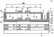
第1フィルタ11は、MEMS技術を利用して形成されており、基板20上に配置され、透過領域S1に固定ミラーM1を有する固定ミラー構造体30と、支持部材40を介して固定ミラー構造体30上に配置され、透過領域S1に可動ミラーM2を有する可動ミラー構造体50と、を備えている。可動ミラー構造体50のエアギャップAGを架橋する部位は、変位可能なメンブレンMEMとなっている。そして、固定ミラー構造体30の電極34と可動ミラー構造体50の電極54の間に印加する電圧に基づいて生じる静電気力(静電引力)によりメンブレンMEMが変位し、エアギャップAGの長さが変化するようになっている。このメンブレンMEMの変位により、エアギャップAGにおけるミラーM1,M2の対向距離、すなわちギャップ長さが変化し、ギャップ長さに応じた所望波長の光を選択的に透過させることができる。
The
固定ミラー構造体30は、基板20の一面上に、絶縁膜22を介して配置されている。本実施形態では、基板20として、例えば単結晶シリコンからなる平面矩形状の半導体基板を採用している。また、基板20の一面上には、シリコン酸化膜やシリコン窒化膜などの絶縁膜22が略均一の厚みをもって形成されている。そして、絶縁膜22を介して、基板20の一面上に固定ミラー構造体30が配置されている。さらに、本実施形態では基板20の一面側表層には、不純物がドーピングされてなる吸収領域21が、垂直方向において、透過領域S1を除く領域に選択的に設けられ、これにより、透過領域S1外での光の透過を抑制するようになっている。この吸収領域21を有さない構成を採用することもできる。
The fixed
固定ミラー構造体30は、例えばポリシリコンからなり、絶縁膜22上に積層された高屈折率下層31と、例えばポリシリコンからなり、該高屈折率下層31上に積層された高屈折率上層32と、を有する。そして、高屈折率下層31と高屈折率上層32との間に、低屈折率層33としての空気層が介在された部位が光学多層膜構造の固定ミラーM1となっている。また、固定ミラーM1は、高屈折率下層31に高屈折率上層32の一部位が接してなる連結部により複数個に分割(細分化)されており、各固定ミラーM1は連結部によって連結されている。また、透過領域S1(固定ミラーM1の形成領域)を除く領域では、高屈折率下層31に高屈折率上層32が接しており、メンブレンMEMの対向部位であって透過領域S1を取り囲む周辺領域T1領域には、電極34が形成されている。なお、符号35は、電極34用のパッドであり、符号36は、低屈折率層33としての空気層をエッチングにより形成するための貫通孔である。
The fixed
一方、可動ミラー構造体50は、例えばポリシリコンからなり、エアギャップAGを架橋して支持部材40上に配置された高屈折率下層51と、例えばポリシリコンからなり、高屈折率下層51上に積層された高屈折率上層52と、を有する。そして、高屈折率下層51と高屈折率上層52との間に、低屈折率層53としての空気層が介在された部位が光学多層膜構造の可動ミラーM2となっている。また、可動ミラーM2は、高屈折率下層51に高屈折率上層52の一部位が接してなる連結部により複数個に分割(細分化)されており、各可動ミラーM2は連結部によって連結されている。この可動ミラーM2は、固定ミラーM1と対向している。また、透過領域S1(可動ミラーM2の形成領域)を除く領域では、高屈折率下層51に高屈折率上層52が接しており、メンブレンMEMであって透過領域S1を取り囲む周辺領域T1領域には、電極54が形成されている。なお、符号55は、電極54用のパッドであり、符号56は、低屈折率層53としての空気層をエッチングにより形成するための貫通孔である。また、符号57は、メンブレンMEMを貫通し、エアギャップAGと外部とを連通させる貫通孔である。この貫通孔57は、エッチングにより支持部材40の一部を除去してエアギャップAGとするための貫通孔である。
On the other hand, the
また、図1に示す符号41は、支持部材40を貫通し、高屈折率上層32に達するコンタクトホールとしての開口部であり、この開口部41に電極34用のパッド35が形成されている。
Further,
このように、ミラー構造体30,50を構成する高屈折率層31,32,51,52としてポリシリコンを採用すると、波長2〜10μm程度の赤外光に対して透明であるので、赤外線ガス検出器の波長選択フィルターとして好適である。なお、ポリシリコン以外にも、ポリゲルマニウムやポリシリコンゲルマニウムなど、シリコン及びゲルマニウムの少なくとも一方を含む半導体薄膜を採用すると、同様の効果を期待することができる。
As described above, when polysilicon is employed as the high refractive index layers 31, 32, 51 and 52 constituting the
加えて、上記したように、ミラーM1,M2の低屈折率層33,53として空気層を採用すると、高屈折率層の屈折率nH(例えばSiでは3.45、Geでは4)と低屈折率層の屈折率nL(空気では1)とのn比(nH/nL)を大きく(例えば3.3以上と)して、上記した波長2〜10μm程度の赤外光を選択的に透過させることのできるファブリペローフィルタを安価に実現することができる。 In addition, as described above, when an air layer is employed as the low refractive index layers 33 and 53 of the mirrors M1 and M2, the refractive index nH (for example, 3.45 for Si and 4 for Ge) of the high refractive index layer is low. The n ratio (nH / nL) to the refractive index nL (1 in the air) of the refractive index layer is increased (for example, 3.3 or more) to selectively transmit the infrared light having the wavelength of about 2 to 10 μm. A Fabry-Perot filter that can be used can be realized at low cost.
ここで、上記した第1フィルタ11は、電極34,54の対向距離の変化量が、該対向距離の初期長さの1/3よりも大きくなると、静電気力がメンブレンMEMのばね復元力を上回り、両ミラー構造体30,50が静電気力で引き込まれ、電圧を除去しても元の状態に戻らなくなる(プルイン現象が生じる)ようになっている。このため、電極34,54の対向距離の初期長さの1/3が、プルイン限界となっている。
Here, in the
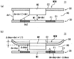
また、上記したように、固定ミラーM1及び可動ミラーM2は光学多層膜構造を有している。そして、各ミラーを構成する層31〜33,51〜53の光学膜厚は、中心波長λcの1/4となっており、固定ミラーM1と可動ミラーM2とで、中心波長λcが互いに等しくなっている。このように、中心波長λcは、各層31〜33、51〜53の光学膜厚によって決定される。この中心波長λcは、図2(a)に示すようにミラーM1,M2の反射帯域の中心位置をなす。また、反射帯域は、中心波長λcを中心とし、その幅が低屈折率層33(53)に対する高屈折率層31,32(51,52)の屈折率比で決定される。なお、同じ屈折率比でも、中心波長λcが長波長であるほど幅は広くなる。
Moreover, as described above, the fixed mirror M1 and the movable mirror M2 have an optical multilayer structure. The optical film thickness of the
図3(a)に示すように、固定ミラーM1及び可動ミラーM2は、反射帯域の波長の光に対して反射作用(高い反射率)を示し、反射帯域外の波長の光に対しては反射率が低く、反射作用を示さない。このミラーM1,M2を対向配置してなる第1フィルタ11(ファブリペローフィルタ)では、図3(b)に示すように光を選択的に透過できる分光帯域がミラーの反射帯域に対応している。本実施形態では、概ね3〜8μmの分光帯域を有している。 As shown in FIG. 3A, the fixed mirror M1 and the movable mirror M2 exhibit a reflection effect (high reflectance) with respect to light with a wavelength in the reflection band, and reflect with respect to light with a wavelength outside the reflection band. The rate is low and does not show a reflection effect. In the first filter 11 (Fabry-Perot filter) formed by arranging the mirrors M1 and M2 so as to face each other, the spectral band capable of selectively transmitting light corresponds to the reflection band of the mirror as shown in FIG. . In this embodiment, it has a spectral band of approximately 3 to 8 μm.
また、第1フィルタ11を選択的に透過する透過スペクトル(干渉光)の波長λは次式で示される。dは、ミラー間のギャップ長さであり、mは干渉光の次数を示す正の整数である。
(数1)λ=2×d/m
実際は、様々な次数の干渉光のうち、上記した分光帯域にピークを有するものが、第1フィルタ11を選択的に透過する。また、ギャップ長さdは、メンブレンMEMの変位にともなって変化する。したがって、メンブレンMEMの変位にともなってギャップ長さdが取り得る範囲において、上記した分光帯域にピークを有する干渉光が、第1フィルタ11を通じて選択的に透過される。したがって、ギャップ長さdの取り得る範囲において、光が選択的に透過される波長域が、図2(b)に例示するように、干渉光の変調帯域となる。
Further, the wavelength λ of the transmission spectrum (interference light) selectively transmitted through the
(Equation 1) λ = 2 × d / m
Actually, among the interference lights of various orders, those having peaks in the above-described spectral band selectively pass through the
電圧が印加されない初期状態(メンブレンMEMが変位する前の状態)において、ミラーM1,M2間のギャップ長さと電極34,54の対向距離が等しいとすると、各次数の変調帯域は、数式1から以下に示すようになる。1次の干渉光(m=1)の変調帯域は、理想的には2di〜di×4/3となる。2次の干渉光(m=2)の変調帯域は、理想的にはdi〜di×2/3となる。3次の干渉光(m=3)の変調帯域は、理想的にはdi×2/3〜di×4/9となる。4次の干渉光(m=4)の変調帯域は、理想的にはdi×1/2〜di×1/3となる。したがって、図4に示すように、1次の干渉光の変調帯域と2次の干渉光の変調帯域との間に、分光不可能な波長帯域(分光不可域)が存在している。また、2次の干渉光の下限(プルイン限界)と3次の干渉光の上限(初期状態)が一致し、これにより、2次の干渉光の変調帯域と3次の干渉光の変調帯域が、隙間無く、且つ、重複する帯域無く、1つの波長域として繋がっている。また、3次の干渉光の下限(プルイン限界)が、4次の干渉光の上限(初期状態)を下回り、これにより、2次の干渉光の変調帯域と3次の干渉光の変調帯域が、一部重複しつつ1つの波長域として繋がっている。
Assuming that the gap length between the mirrors M1 and M2 and the facing distance between the
本実施形態では、初期状態のギャップ長さdiが、第1フィルタ11の分光帯域の上限(本実施形態では8μm)とほぼ同じ長さに設定されている。このため、第1フィルタ11の分光帯域内には、2次の干渉光、3次の干渉光、4次の干渉光の各変調帯域が位置し、第1フィルタ11から、2次の干渉光、3次の干渉光、及び4次の干渉光の、3つの次数の干渉光が透過されるようになっている。
In the present embodiment, the gap length di in the initial state is set to substantially the same length as the upper limit of the spectral band of the first filter 11 (8 μm in the present embodiment). Therefore, the modulation bands of the second order interference light, the third order interference light, and the fourth order interference light are located within the spectral band of the
次に、残りの第2フィルタ12、赤外線検出器13、及び補正処理部14について説明する。
Next, the remaining
第2フィルタ12は、所定帯域の光(任意の次数の干渉光の変調帯域に応じた光)を選択的に透過させるバンドパス部60を有している。バンドパス部60は、光学多層膜構造の所謂バンドパスフィルターであり、図1及び図2に示すように、ミラーM1,M2の形成領域、すなわち第1フィルタ11の透過領域S1に対応して設けられている。また、バンドパス部60として、異なる次数の干渉光それぞれに対応する複数種類のバンドパス部60a〜60cを有する。各バンドパス部60a〜60cは、対応する次数の干渉光の変調帯域に応じた光透過特性を有している。
The
本実施形態では、バンドパス部60aが、2次の干渉光の変調帯域において光を選択的に透過させる特性を有し、バンドパス部60bが、3次の干渉光の変調帯域において光を選択的に透過させる特性を有する。また、バンドパス部60cが、4次の干渉光の変調帯域において光を選択的に透過させる特性を有する。したがって、第1フィルタ11を透過した干渉光のうち、バンドパス部60aからは2次の干渉光が透過される。また、バンドパス部60bからは、主として3次の干渉光が透過される。また、バンドパス部60cからは、主として4次の干渉光が透過される。なお、図1では、便宜上、細分化されたミラーM1,M2の1つ(一対)につき1つのバンドパス部60が対応しているように図示している。しかしながら、複数対のミラーM1,M2に対応して1つのバンドパス部60を設けても良い。また、細分化されたミラーM1,M2ではなく、透過領域S1にミラーM1,M2がそれぞれ1つ設けられる場合には、1つのミラーM1,M2の互いに異なる一部に対応するように複数のバンドパス部60a〜60cを設ければ良い。
In the present embodiment, the
上記したように、3次の干渉光と4次の干渉光は変調帯域が一部重複する。このため、3次の干渉光が、ギャップ長さが初期状態diから所定範囲のときにとり得る領域Aに位置すると、バンドパス部60bから3次の干渉光だけでなく、4次の干渉光も透過される。また、4次の干渉光が、ギャップ長さがプルイン限界から所定範囲のときにとり得る領域Bに位置すると、バンドパス部60cから4次の干渉光だけでなく、3次の干渉光も透過される。領域A,Bについては後述する。
As described above, the modulation bands of the third-order interference light and the fourth-order interference light partially overlap. For this reason, when the third-order interference light is located in the region A that can be taken when the gap length is within a predetermined range from the initial state di, not only the third-order interference light but also the fourth-order interference light from the
また、本実施形態では、図2に示すように、複数のバンドパス部60a〜60cが、受光面の形状及び受光面積が互いに等しく、垂直方向においてミラーM1,M2(透過領域S1)の中心C1に対し同心円上に配置されている。このような配置とすると、バンドパス部60a〜60cに対応して設けられる各赤外線検出素子70a〜70cが検出する光の強度のばらつきを抑制することができる。すなわち、各赤外線検出素子70a〜70cで感度をほぼ同一とすることができる。なお、図2では受光面の形状として真円の例を示すが、特に形状は限定されるものではない。
In the present embodiment, as shown in FIG. 2, the plurality of
また、本実施形態では、バンドパス部60a〜60cが、金属からなる基材61に保持されており、第2フィルタ12がバンドパスフィルタアレイとなっている。基材61は、第1フィルタ11を透過した干渉光を透過させないマスク(非透過部)としての機能を果たす。この基材61における透過領域S1に対応する部分に、バンドパス部60a〜60cの配置部分に対応して貫通孔が設けられている。貫通孔における第1フィルタ11と反対側の開口近傍の内壁が、図1に示すように縮径しており、この縮径部にバンドパス部60a〜60cが搭載されている。
Moreover, in this embodiment, the
赤外線検出器13は、第2フィルタ12を透過した干渉光を、バンドパス部60の種類ごとに異なる赤外線検出素子70にて検出するように、複数の赤外線検出素子70を有している。本実施形態では、3つのバンドパス部60a〜60cに対応して3つの赤外線検出素子70a〜70cを有する。なお、赤外線検出素子70の個数は、バンドパス部60の個数と同数に限定されるものではない。例えば2次の干渉光用のバンドパス部60aを複数有し、これら複数のバンドパス部60aに対応して1つの赤外線検出素子70aを設けても良い。また、1つのバンドパス部60aに対応して複数の赤外線検出素子70aを設けても良い。
The
赤外線検出素子70としては、ボロメータ、熱電堆(サーモパイル)、焦電型素子、量子型素子などを採用することができる。本実施形態では、赤外線検出器13が、例えばシリコンやゲルマニウムからなる基板71の第2フィルタ12側の一面上に形成された熱電堆と、該熱電堆の少なくとも一部を被覆するように設けられた赤外線吸収膜を備えた熱型の赤外線検出素子70a〜70cを有している。
As the infrared detecting
また、バンドパス部60aを透過した干渉光(2次の干渉光)が赤外線検出素子70aに入射し、バンドパス部60bを透過した干渉光(主として3次の干渉光)が赤外線検出素子70bに入射するようになっている。さらに、バンドパス部60cを透過した干渉光(主として4次の干渉光)が赤外線検出素子70cに入射するようになっている。
Further, interference light (secondary interference light) transmitted through the
補正処理部14は、連続する2つの次数の干渉光それぞれに対応する2つのバンドパス部の一方を、連続する2つの次数の干渉光が透過する帯域において、連続する2つの次数の干渉光が透過するバンドパス部に対応した赤外線検出素子の出力を、連続する2つの次数の干渉光の一方のみが透過するバンドパス部に対応した赤外線検出素子の出力に基づいて補正処理するものである。
The
本実施形態では、3次の干渉光と4次の干渉光の変調帯域が一部重複するため、3次の干渉光の波長が図5に示す領域Aにあるときに、3次の干渉光に対応するバンドパス部60bから、3次の干渉光とともに4次の干渉光が透過される。このため、バンドパス部60bに対応する赤外線検出素子70bには、3次の干渉光と4次の干渉光が入射し、その出力は2つの干渉光の影響を受ける。
In this embodiment, since the modulation bands of the third-order interference light and the fourth-order interference light partially overlap, the third-order interference light is present when the wavelength of the third-order interference light is in the region A shown in FIG. The fourth-order interference light is transmitted together with the third-order interference light from the band-
しかしながら、3次の干渉光の波長が図5に示す領域Aにあるとき、4次の干渉光に対応するバンドパス部60cからは4次の干渉光のみが透過される。このため、4次のバンドパス部60cに対応する赤外線検出素子70cの出力は、4次の干渉光の影響のみを受ける。補正処理部14は、3次の干渉光の波長が図5に示す領域Aにあるとき、赤外線検出素子70cの出力に基づいて、赤外線検出素子70bの出力における4次の干渉光の影響分を補正する。例えば、赤外線検出素子70bの出力と赤外線検出素子70cの出力の差分を、赤外線検出素子70bによる3次の干渉光の影響分とする。
However, when the wavelength of the third-order interference light is in the region A shown in FIG. 5, only the fourth-order interference light is transmitted from the
同様に、、4次の干渉光の波長が図5に示す領域Bにあるとき、4次の干渉光に対応するバンドパス部60cから、4次の干渉光とともに3次の干渉光が透過される。一方、3次の干渉光に対応するバンドパス部60bからは3次の干渉光のみが透過される。補正処理部14は、4次の干渉光の波長が図5に示す領域Bにあるとき、赤外線検出素子70bの出力に基づいて、赤外線検出素子70cの出力における3次の干渉光の影響分を補正する。例えば、赤外線検出素子70cの出力と赤外線検出素子70bの出力の差分を、赤外線検出素子70cによる4次の干渉光の影響分とする。
Similarly, when the wavelength of the fourth-order interference light is in the region B shown in FIG. 5, the third-order interference light is transmitted together with the fourth-order interference light from the
これにより、3次の干渉光と4次の干渉光の変調領域が重複領域を有しながらも、3次の干渉光と4次の干渉光をそれぞれ検出することができる。なお、2次の干渉光については、他の干渉光と変調帯域が重複しないため、補正処理部14にて補正は行わず、赤外線検出素子70aの出力をそのまま出力する。
As a result, the third-order interference light and the fourth-order interference light can be detected while the modulation areas of the third-order interference light and the fourth-order interference light have overlapping regions. As for the secondary interference light, the modulation band does not overlap with other interference light, so that the
次に、プルイン限界を初期状態の電極34,54の対向距離の1/3とする第1フィルタ11を備えた、上記波長選択型赤外線検出装置10の特徴部分の効果について説明する。
Next, the effect of the characteristic part of the wavelength selective infrared detecting
本実施形態では、第1フィルタ11を構成する一対のミラーM1,M2が、シリコンからなる高屈折率層31,32,51,52間に、空気からなる低屈折率層33,53が介在されてなるエアミラーとなっている。このため、第1フィルタ11の分光帯域を広くとることができる。また、初期状態のギャップ長さが第1フィルタ11の分光帯域の上限と同じ長さとされており、第2フィルタ12が、2次、3次、4次の各干渉光に対応したバンドパス部60a〜60cを有する。このため、第1フィルタ11の分光帯域のほぼ全域を、第1フィルタ及び第2フィルタによる透過スペクトルの変調帯域とすることができる。さらには、3次の干渉光に対応するバンドパス部60b及び4次の干渉光に対応するバンドパス部60cの一方を3次の干渉光と4次の干渉光が透過する領域A,Bにおいて、3次の干渉光及び4次の干渉光が透過するバンドパス部に対応した赤外線検出素子の出力を、3次の干渉光及び4次の一方の干渉光が透過するバンドパス部に対応した赤外線検出素子の出力に基づいて補正処理する補正処理部14を備える。したがって、3次の干渉光と4次の干渉光の変調領域が重複領域を有しながらも、実質的に3次の干渉光、4次の干渉光をそれぞれ検出することができる。したがって、2次の干渉光の変調帯域の上限から4次の干渉光の変調帯域の下限までの範囲、換言すれば分光帯域全域において、所定波長の光を選択的に検出することができる。
In the present embodiment, the pair of mirrors M1 and M2 constituting the
なお、本実施形態では、第2フィルタ12が2次〜4次の干渉光用のバンドパス部60a〜60cを有する例を示した。しかしながら、第2フィルタ12を透過する干渉光の次数は上記例に限定されるものではない。少なくとも可変ファブリペロー型の第1フィルタ11が、ギャップ長さに応じた複数の次数の干渉光を透過させ、第2フィルタ12の各バンドパス部60が、複数の次数の干渉光のうち、自身の光透過特性に応じた波長の光をそれぞれ選択的に透過させる。そして、バンドパス部60を透過した干渉光が、バンドパス部60の光透過特性ごとに異なる赤外線検出素子70にて検出されればよい。例えば、第1フィルタ11から1次〜4次の干渉光が透過され、第2フィルタ12が、1次〜4次の干渉光のうち、1次、2次、4次の干渉光を透過させるように、1次、2次、4次の干渉光に対応した3つのバンドパス部60を有する構成としても良い。各バンドパス部60を透過できる干渉光の変調帯域の足し合わせが、第1フィルタ及び第2フィルタによる波長選択フィルタの透過スペクトルの変調帯域となるため、第1フィルタ11を1つのみ有する構成において、従来よりも広い波長域において所定波長の光を選択的に検出することができる。
In the present embodiment, an example in which the
なかでも、本実施形態に示したように、第2フィルタ12が、連続する複数の次数の干渉光について、バンドパス部60を有する構成とすると良い。干渉光の変調帯域が互いに近いため、分光帯域内に、各干渉光の変調帯域が位置するように調整しやすい。すなわち、第1フィルタ11を構成しやすい。また、干渉光の次数によっては、複数の変調帯域を、連続する1つの変調帯域とすることもできる。
In particular, as shown in the present embodiment, the
また、本実施形態では、第2フィルタ12が、連続する複数の次数の干渉光として、2次〜4次の干渉光用のバンドパス部60a〜60cを有したが、2次と3次の干渉光用のバンドパス部60a,60bのみを有する構成や、3次と4次の干渉光用のバンドパス部60b,60cのみを有する構成を採用することもできる。2次と3次の干渉光用のバンドパス部60a,60bのみを有する場合、補正処理部14を不要とすることができる。
Further, in the present embodiment, the
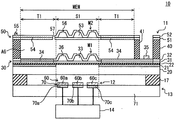
例えば、2次と3次の干渉光用のバンドパス部60a,60bのみを有する例としては、図6に示す構成を採用することができる。図6に示す波長選択型赤外線検出装置10では、第1フィルタ11において、一対のミラーM1,M2が、シリコンの半導体薄膜からなる高屈折率層31,32,51,52間に、シリコンよりも低屈折率の二酸化シリコンからなる低屈折率層33,53が介在されてなる光学多層膜構造を有している。そして、初期状態のギャップ長さが第1フィルタ11の分光帯域の上限とほぼ同じ長さとされている。また、第2フィルタ12が、2次、3次の各干渉光に対応したバンドパス部60a,60bを有しており、赤外線検出器13がバンドパス部60a,60bに対応した赤外線検出素子70a,70bを有している。
For example, as an example having only the
このような構成とすると、シリコンを高屈折率層31,32,51,52とし、二酸化シリコンを低屈折率層33,53とするミラーM1,M2において、2次干渉光の変調帯域の上限が、第1フィルタ11の分光帯域(概ね3〜6μm)の上限とほぼ一致し、3次干渉光の変調帯域の下限が分光帯域の下限とほぼ一致することとなる。したがって、第1フィルタ11の分光帯域のほぼ全域を、第1フィルタ11及び第2フィルタ12による透過スペクトルの変調帯域とすることができる。
With such a configuration, in the mirrors M1 and M2 in which silicon is the high refractive index layers 31, 32, 51, and 52 and silicon dioxide is the low refractive index layers 33 and 53, the upper limit of the modulation band of the secondary interference light is Thus, the upper limit of the spectral band (approximately 3 to 6 μm) of the
また、本実施形態では、スペーサ16を介して第2フィルタ12と赤外線検出器13が積層配置される例を示した。しかしながら、例えば図7に示すように、第2フィルタ12を構成するバンドパス部60a〜60cが、赤外線検出器13の対応する赤外線検出素子70a〜70c上に積層配置された構成としても良い。このような構成とすると、バンドパス部60の直下に赤外線検出素子70が存在するため、赤外線検出素子70の感度を向上しつつ積層方向において波長選択型赤外線検出装置10の体格を小型化することができる。なお、図7に示す例では、赤外線検出素子70として、例えばシリコンやゲルマニウムからなる基板71の第2フィルタ12側の表層に、p導電型又はn導電型の不純物が注入されてなるボロメータが形成されている。この場合、赤外線検出素子70としてのボロメータに所定の検出電圧を印加しておくことで、赤外線吸収の温度変化による赤外線検出素子70の抵抗変化に基づき、赤外線を検出することができる。また、図7に示す符号17は、赤外線検出器13の基板71と第1フィルタ11の間に介在されたスペーサである。
Further, in the present embodiment, an example in which the
(第2実施形態)
本実施形態では、第1フィルタ11が、第1実施形態同様、一対のミラー構造体30,50を有する。そして、可動ミラー構造体50のエアギャップAGを架橋する部分が、変位可能なメンブレンMEMとなっている。また、初期状態のギャップ長さdiの2倍の長さが第1フィルタ11の分光帯域の上限とほぼ同じ長さとなっており、対向配置されたミラーM1,M2間のギャップ長さの変化量を、初期状態のギャップ長さdiの1/2以上とすることができる。そして、第2フィルタ12が、連続する複数の次数の干渉光として、1次の干渉光に対応したバンドパス部60と2次の干渉光に対応したバンドパス部60を有する点を主たる特徴点とする。
(Second Embodiment)
In the present embodiment, the
このような、ミラーM1,M2間のギャップ長さの変化量を初期状態のギャップ長さdiの1/2以上とすることができる第1フィルタ11について、その一例を説明する。本実施形態に示す第1フィルタ11は、本出願人により先になされた特願2010−261490号に記載のものであるため、詳細については参照されたい。
An example of the
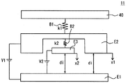
図8は、本実施形態に係る第1フィルタ11を、ばね変形部と電極とで簡易モデル化した図である。図8では、電極E1(第1実形態の電極34に相当)に電極E2(第1実施形態の電極54に相当)が対向配置され、電極E1,E2はばね変形部B1にて接続されている。また、電極E1に電極E3が対向配置され、電極E3はばね変形部B2にて電極E2と接続されている。すなわち、2つのばね変形部B1,B2と2つの電極対を有している。また、3つの電極E1〜E3のうち、電極E1の位置が固定され、電極E2,E3が変位可能となっている。
FIG. 8 is a diagram in which the
ここで、ばね変形部B1のばね定数をk1、ばね変形部B2のばね定数をk2、電極対E1,E2に印加する電圧をV1、電極対E1,E3に印加する電圧をV2、電極E1,E2の対向距離及び電極E1,E3の初期長さ(電圧が印加されない状態での長さ)をともにdiとする。また、電圧V1,V2を印加したときの電極E2の絶対変位量をx1、同じく電圧V1,V2を印加したときの電極E3の絶対変位量をx2、大気中の誘電率をε、電極E1,E2の対向面積をS1、電極E1,E3の対向面積をS2とする。 Here, the spring constant of the spring deformation portion B1 k 1, the spring constant k 2 of the spring deformation portion B2, V 1 the voltage applied to the electrode pair E1, E2, the voltage applied to the electrode pair E1, E3 V 2 The opposing distance between the electrodes E1 and E2 and the initial length of the electrodes E1 and E3 (the length when no voltage is applied) are both di. Further, x 1 the absolute amount of displacement of the electrode E2 when a voltage is applied to V1, V2, also the absolute amount of displacement x 2 electrodes E3 upon application of voltages V1, V2, the dielectric constant in the air epsilon, electrode E1, E2 facing area of S 1, the opposing area of the electrodes E1, E3 and S 2.
電極E2に働く力の釣り合いは、電圧V1,V2の印加による電極E2の変位x1でのばね変形部B1の復元力と、電極E2の変位x1での電圧V1の印加にて生じる静電気力との釣り合いで決定され、下記式2で示される。
(数2)k1x1=k2(x2−x1)+εS1V1 2/{2(di−x1)2}
一方、電極E3に働く力の釣り合いは、電圧V1,V2に印加による、電極E2の変位x1と電極E3の変位x2でのばね変形部B2の復元力と、電極E3の変位x2での電圧V2の印加にて生じる静電気力との釣り合いで決定され、下記式3で示される。
(数3)k2(x2−x1)=εS2V2 2/{2(di−x2)2}
プルイン限界は、これら数式2,3において、変位x1とx2が最大の接点解を持つ状態であり、数値計算によって算出することができる。
Balance of forces acting on the electrode E2 is the electrostatic force generated by application of the voltage V1 of the restoring force of the spring deformation portion B1 of the displacement x 1 of the electrode E2 by application of voltages V1, V2, the displacement x 1 of the electrode E2 And is shown by the following
(Expression 2) k 1 x 1 = k 2 (x 2 −x 1 ) + εS 1 V 1 2 / {2 (di−x 1 ) 2 }
On the other hand, the balance of forces acting on the electrode E3 is by applying a voltage V1, V2, and the restoring force of the spring deformation portion B2 of the displacement x 2 of the displacement x 1 and the electrode E3 of the electrode E2, the displacement x 2 electrodes E3 Is determined by the balance with the electrostatic force generated by the application of the voltage V2, and is expressed by the following
(Expression 3) k 2 (x 2 −x 1 ) = εS 2 V 2 2 / {2 (di−x 2 ) 2 }
Pull limit, in these
図9は、算出した電極E3の変位x2の最大値の、ばね定数比k1/k2に対する依存性を示す図である。ばね定数比k1/k2を1よりも大きくする、すなわちばね定数k2をばね定数k1よりも小さくすると、電極E3の変位量を初期長さdiの1/3(0.33)よりも大きくすることができる。なお、ばね定数比k1/k2を無限大とすると、x2=5di/9となる。すなわち、理想的には、初期長さdiの5/9(0.56)まで変位させることができる。 9, the maximum value of the displacement x 2 of the calculated electrode E3, a diagram showing the dependence on the spring constant ratio k 1 / k 2. When the spring constant ratio k 1 / k 2 is made larger than 1, that is, the spring constant k 2 is made smaller than the spring constant k 1 , the displacement amount of the electrode E3 is calculated from 1/3 (0.33) of the initial length di. Can also be increased. If the spring constant ratio k 1 / k 2 is infinite, x 2 = 5 di / 9. In other words, it can be ideally displaced to 5/9 (0.56) of the initial length di.
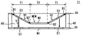
次に、図8に示す簡易モデルの構成を適用した第1フィルタ11について説明する。図10に示す第1フィルタ11は、透過領域S1に固定ミラーM1を有する固定ミラー構造体30と、透過領域S1に可動ミラーM2を有する可動ミラー構造体50と、を備える。可動ミラー構造体50において、可動ミラーM2を含み、エアギャップAGを介して固定ミラー構造体30と対向する部分が変位可能なメンブレンMEMとされ、該メンブレンMEMを除く部分の少なくとも一部が、支持部材40によって固定ミラー構造体30上に支持されている。なお、メンブレンMEMに構成された可動ミラーM2は、固定ミラーM1に対向配置されている。
Next, the
また、メンブレンMEMにおける透過領域S1(可動ミラーM2の形成領域)を除く周辺領域T1には、複数のばね変形部が、透過領域S1をそれぞれ取り囲みつつ多重に設けられている。これらばね変形部は、メンブレンMEMの外周端からメンブレンMEMの中心に向かう方向においてメンブレンMEMの中心に近いばね変形部ほどばね定数が小さく設定されている。図10に示す例では、複数のばね変形部として、図8のモデル同様、2つのばね変形部B1,B2を有している。そして、メンブレンMEMの中心に近いばね変形部B2のばね定数k2が、メンブレンMEMの外周端に近いばね変形部B1のばね定数k1よりも小さくなっており、さらには2つのばね変形部B1,B2のばね定数比k1/k2が7以上となっている。 Further, in the peripheral region T1 excluding the transmission region S1 (formation region of the movable mirror M2) in the membrane MEM, a plurality of spring deforming portions are provided in a multiple manner so as to surround the transmission region S1. The spring constants of these spring deformed portions are set to be smaller as the spring deformed portions are closer to the center of the membrane MEM in the direction from the outer peripheral end of the membrane MEM toward the center of the membrane MEM. In the example shown in FIG. 10, two spring deformable portions B <b> 1 and B <b> 2 are provided as a plurality of spring deformable portions as in the model of FIG. 8. Then, the spring constant k 2 of the spring deformation portion B2 closer to the center of the membrane MEM is, is smaller than the spring constant k 1 of the spring deformation portion B1 closer to the outer peripheral edge of the membrane MEM, further two spring deformation portion B1 , B2 has a spring constant ratio k 1 / k 2 of 7 or more.
また、メンブレンMEM及び固定ミラー構造体30のメンブレン対向部位の周辺領域T1には、互いに対向するように電極が設けられて電極対が構成されている。この電極対は、透過領域S1を取り囲みつつ複数のばね変形部に対応してばね変形部と同数の多重に設けられるとともに、複数の電極対はそれぞれ独立して電圧を印加できるように電気的に分離されている。図10に示す例では、可動ミラー構造体50のメンブレンMEMに、複数の電極E2,E3が、透過領域S1を取り囲みつつ複数のばね変形部B1,B2に対応してばね変形部B1,B2と同数の多重に設けられている。より詳しくは、メンブレンMEMの外周端側から、ばね変形部B1、電極E2、ばね変形部B2、電極E3、そして可動ミラーM2の順となっている。また、電極E2,E3に対向して、固定ミラー構造体30に電極E1が設けられている。すなわち、メンブレンMEMの外周端にばね変形部B1が設けられ、メンブレンMEMの外周端からメンブレンMEMの中心に向かう方向において、複数のばね変形部B1,B2と複数の電極対(電極対E1,E2と電極対E1,E3)が交互に設けられている。また、メンブレンMEMにおいて、各電極対を構成する電極E2,E3の剛性が、ばね変形部B1,B2いずれの剛性よりも高くなっている。
Further, in the peripheral region T1 of the membrane facing part of the membrane MEM and the fixed
このような構成の第1フィルタ11では、最外周のばね変形部B1に対応する最外周の電極対E1,E2(第1電極対)に電圧V1を印加することで、該電極対E1,E2に生じる静電気力により、複数のばね変形部B1,B2のうち、最外周のばね変形部B1を変形させることができる。この電圧V1の印加では、メンブレンMEM全体が変位することとなる。また、例えば最外周の電極対E1,E2よりも内側に位置する電極対E1,E3(第2電極対)に電圧V2を印加することで、該電極対E1,E3に生じる静電気力により、ばね定数の関係(k1>k2)から最外周のばね変形部B1を殆ど変形させずに、内側に位置するばね変形部B2を変形させることができる。本実施形態では、ばね定数の関係(k1>k2)から、電極対E1,E3に生じる静電気力を、電極対E1,E2に生じる静電気力よりも小さくしている。
In the
このため、最外周の電極対E1,E2に電圧V1を印加してメンブレンMEMの透過領域S1部分(可動ミラーM2)を変位させた状態で、内側に位置する電極対E1,E3に電圧V2を印加することで、電極E3よりも内側に位置するメンブレンMEMの透過領域S1部分を、図10に示すようにさらに変位させることができる。理想的には、ミラーM1,M2の初期状態のギャップ長さを電極E1,E3の対向距離同様diとすると、電極対E1,E2に生じる静電気力により、ミラーM2を初期状態のギャップ長さdiの1/3変位させる。これにより、ミラーM1,M2のギャップ長さは初期状態の長さdiの2/3となる。そして、電極対E1,E3に生じる静電気力により、ミラーM2を初期状態のギャップ長さdiの2/3に対してさらに1/3変位させる。すなわち、理想的には、トータルで、ミラーM2を初期状態のギャップ長さdiの5/9変位させることができる。このように、各電極対に電圧を印加する期間を少なくとも一部重複させ、該重複期間において各電極対に生じる静電気力により、メンブレンMEMを、従来のプルイン限界(初期状態の電極の対向距離の1/3)を超えて変位させることができる。 For this reason, the voltage V2 is applied to the inner electrode pair E1, E3 in a state where the transmission region S1 portion (movable mirror M2) of the membrane MEM is displaced by applying the voltage V1 to the outermost electrode pair E1, E2. By applying, the transmission region S1 portion of the membrane MEM located inside the electrode E3 can be further displaced as shown in FIG. Ideally, assuming that the gap length in the initial state of the mirrors M1 and M2 is di as in the facing distance of the electrodes E1 and E3, the mirror length of the mirror M2 in the initial state is caused by the electrostatic force generated in the electrode pair E1 and E2. 1/3 displacement. Thereby, the gap length of the mirrors M1 and M2 becomes 2/3 of the initial length di. The mirror M2 is further displaced by 1/3 with respect to 2/3 of the gap length di in the initial state by electrostatic force generated in the electrode pair E1, E3. In other words, ideally, the mirror M2 can be displaced 5/9 of the initial gap length di in total. In this manner, at least part of the period in which the voltage is applied to each electrode pair is overlapped, and the membrane MEM is made to have a conventional pull-in limit (the opposing distance between the electrodes in the initial state) by the electrostatic force generated in each electrode pair during the overlap period. 1/3) can be displaced.
また、本実施形態では、初期状態で、電極E1,E2の対向距離及び電極E1,E3の対向距離が等しく、ミラーM1,M2間のギャップ長さが、電極E1,E2の対向距離及び電極E1,E3の対向距離以下となっている。したがって、ミラーM1,M2間のギャップ長さの変化量を、初期状態のギャップ長さdiの1/3よりも大きくすることができる。 In this embodiment, in the initial state, the facing distance between the electrodes E1 and E2 and the facing distance between the electrodes E1 and E3 are equal, and the gap length between the mirrors M1 and M2 is equal to the facing distance between the electrodes E1 and E2 and the electrode E1. , E3 or less. Therefore, the amount of change in the gap length between the mirrors M1 and M2 can be made larger than 1/3 of the gap length di in the initial state.
さらに、本実施形態では、2つのばね変形部B1,B2のばね定数比k1/k2が7以上となっている。したがって、図9に示したように、電極E1,E3の対向距離の変化量を、初期状態のギャップ長さdiの1/2よりも大きくすることができる。なお、ばね定数比k1/k2が6で、電極E1,E3の対向距離の変化量が、初期長さdiの1/2よりも若干小さく、ばね定数比k1/k2が7で、電極E1,E3の対向距離の変化量が初期状態のギャップ長さdiの1/2よりも大きくなる。
Further, in the present embodiment, the spring constant ratio k 1 / k 2 between the two spring deformation portions B1 and B2 is 7 or more. Therefore, as shown in FIG. 9, the amount of change in the facing distance between the electrodes E1 and E3 can be made larger than 1/2 of the gap length di in the initial state. It should be noted that the spring constant ratio k 1 / k 2 is 6, the amount of change in the facing distance between the
ここで、電圧が印加されない初期状態において、ミラーM1,M2間のギャップ長さdiと電極E1,E2の対向距離及び電極E1,E3の対向距離が等しく、ミラーM2を初期状態のギャップ長さdiの1/2変位させることができるとすると、各次数の変調帯域は、上記した数式1から以下に示すようになる。1次の干渉光(m=1)の変調帯域は、理想的には2di〜diとなる。2次の干渉光(m=2)の変調帯域は、理想的にはdi〜di×1/2となる。3次の干渉光(m=3)の変調帯域は、理想的にはdi×2/3〜di×1/3となる。4次の干渉光(m=4)の変調帯域は、理想的にはdi×1/2〜di×1/4となる。したがって、図11に示すように、1次の干渉光の下限(プルイン限界)と2次の干渉光の上限(初期状態)が一致し、これにより、1次の干渉光の変調帯域と2次の干渉光の変調帯域が、隙間無く、且つ、重複する帯域無く、1つの波長域として繋がる。なお、ミラーM2を初期状態のギャップ長さdiの1/2変位させることができるとすると、1次の干渉光の下限(プルイン限界)が、2次の干渉光の上限(初期状態)を下回り、これにより、1次の干渉光の変調帯域と2次の干渉光の変調帯域が、一部重複しつつ1つの波長域として繋がる。
Here, in the initial state in which no voltage is applied, the gap length di between the mirrors M1 and M2, the opposing distance between the electrodes E1 and E2, and the opposing distance between the electrodes E1 and E3 are equal, and the mirror M2 is in the initial gap length di. If it can be displaced by 1/2, the modulation band of each order is as shown below from
図12(a),(b)は、1次の干渉光と2次の干渉光の変調帯域を示している。図12(a),(b)は、本実施形態同様、初期状態で、ミラーM1,M2間のギャップ長さdiと電極E1,E2の対向距離及び電極E1,E3の対向距離が等しい構成での結果を示している。比較例として示す図12(a)では、初期長さdi(4200nm)に対し、プルイン限界の2800nm(di×1/3)までしか可動ミラーM2を変位させることができないため、1次干渉光の変調帯域が狭く、1次の干渉光の変調帯域と2次の干渉光の変調帯域の間に、分光不可域が存在している。これに対し、2つのばね変形部B1,B2のばね定数比k1/k2を7以上とした構成では、図12(b)に示すように、1次の干渉光の変調帯域と2次の干渉光の変調帯域が、連続して1つの帯域となっている。なお、図12(b)では、エアギャップ4200nmが初期長さdiであり、エアギャップ2100nmが可動ミラーM2を初期長さdiの1/2変位させた状態を示している。 FIGS. 12A and 12B show the modulation bands of the primary interference light and the secondary interference light. 12A and 12B, in the initial state, as in this embodiment, the gap length di between the mirrors M1 and M2, the opposing distance between the electrodes E1 and E2, and the opposing distance between the electrodes E1 and E3 are the same. Shows the results. In FIG. 12A shown as a comparative example, the movable mirror M2 can be displaced only up to the pull-in limit of 2800 nm (di × 1/3) with respect to the initial length di (4200 nm). The modulation band is narrow, and there is a non-spectral region between the modulation band of the primary interference light and the modulation band of the secondary interference light. On the other hand, in the configuration in which the spring constant ratio k 1 / k 2 of the two spring deformable portions B1 and B2 is 7 or more, as shown in FIG. The modulation band of the interference light is continuously one band. FIG. 12B shows a state in which the air gap 4200 nm is the initial length di and the air gap 2100 nm has displaced the movable mirror M2 by 1/2 of the initial length di.
このように、2つのばね変形部B1,B2のばね定数比k1/k2を7以上とすると、1次の干渉光の変調帯域を広くして、1次の干渉光の変調帯域と2次の干渉光の変調帯域を連続させることができる。すなわち、分光不可域を無くすことができる。
As described above, when the spring constant ratio k 1 / k 2 of the two spring
また、本実施形態では、初期状態のギャップ長さdiの2倍の長さが第1フィルタ11の分光帯域(例えば第1実施形態同様8μm)の上限とほぼ同じ長さとなっている。したがって、1次干渉光の変調帯域の上限が、第1フィルタ11の分光帯域の上限とほぼ一致し、2次の干渉光の変調帯域の下限が、第1フィルタ11の分光帯域の下限とほぼ一致する。このため、第1フィルタ11の分光帯域内には、1次の干渉光、2次の干渉光の各変調帯域が位置し、第1フィルタ11から、1次の干渉光と2次の干渉光の、2つの次数の干渉光が透過される。
In the present embodiment, the length twice as large as the gap length di in the initial state is substantially the same as the upper limit of the spectral band of the first filter 11 (for example, 8 μm as in the first embodiment). Therefore, the upper limit of the modulation band of the first order interference light substantially coincides with the upper limit of the spectral band of the
また、図示しないが、第2フィルタ12が、連続する複数の次数の干渉光として、1次の干渉光に対応したバンドパス部60と2次の干渉光に対応したバンドパス部60を有している。さらに、赤外線検出器13が、バンドパス部60それぞれに対応する赤外線検出素子70を有している。
Although not shown, the
以上から、本実施形態に係る波長選択型赤外線検出装置10によれば、1次の干渉光の変調帯域の上限から2次の干渉光の変調帯域の下限までの連続する1つの広い波長域において、所定波長の光を選択的に検出することができる。また、干渉光は次数が小さいほど変調帯域が広いので、1次の干渉光と2次の干渉光を利用する本実施形態によれば、所定波長の光を選択的に検出することができる波長域をより広くすることができる。また、分光帯域のほぼ全域において、所定波長の光を選択的に検出することができる。
From the above, according to the wavelength selective
なお、ばね変形部B1,B2のばね定数比k1/k2が7の場合、1次の干渉光の下限(プルイン限界)と2次の干渉光の上限(初期状態)が一致し、変調帯域が重複しないので、第1実施形態に示した補正処理部14が不要である。一方、ばね変形部B1,B2のばね定数比k1/k2が7より大きいと、1次の干渉光の下限(プルイン限界)が2次の干渉光の上限(初期状態)を下回り、変調帯域が重複する。この場合、第1実施形態に示した補正処理部14を備えれば良い。本実施形態の補正処理部14は、1次の干渉光に対応するバンドパス部60及び2次の干渉光に対応するバンドパス部60の一方を1次の干渉光と2次の干渉光が透過する帯域において、1次の干渉光及び2次の干渉光が透過するバンドパス部60に対応した赤外線検出素子70の出力を、1次の干渉光及び2次の一方の干渉光が透過するバンドパス部60に対応した赤外線検出素子70の出力に基づいて補正処理する。したがって、1次の干渉光の変調帯域と2次の干渉光の変調帯域が重複しながらも、これらの変調帯域の全域を、連続する1つの変調帯域とすることができる。したがって、所定波長の光を選択的に検出することができる波長域をより広くすることができる。
When the spring constant ratio k 1 / k 2 of the spring deformed portions B1 and B2 is 7, the lower limit (pull-in limit) of the first order interference light and the upper limit (initial state) of the second order interference light match, and the modulation Since the bands do not overlap, the
なお、図10に示す第1フィルタ11では、電極E2,E3の剛性がばね変形部B1,B2よりも高くされ、電極E2,E3とばね変形部B1,B2とが電気的に分離されている。すなわち、電極E2,E3とばね変形部B1,B2が構造的に分離されている。したがって、電極対をなす電極E2,E3を平行に保ったまま、ばね変形部B1,B2を変形させて、メンブレンMEMを変位させることができる。これにより、電極E3に接続された可動ミラーM2と固定ミラーM1との対向距離の制御性を向上することができる。そして、透過波長の半値幅(FWHM)を小さくする、すなわち分解能を向上することができる。しかしながら、メンブレンMEMにおいて、電極対を構成する電極E2,E3がばね変形部B1,B2を兼ねる構成としても良い。具体的には、電極E2がばね変形部B1を兼ね、電極E3がばね変形部B2を兼ねても良い。これによれば、電極E2,E3とばね変形部B1,B2が構造的に分離される構成に較べて、構成を簡素化し、垂直方向において、第1フィルタ11の体格を小型化することも可能である。
In the
また、可動ミラー構造体50が互いに電気的に分離された複数の電極E2,E3を有し、固定ミラー構造体30が、複数の電極E2,E3に対向配置された1つの電極E1を有する例を示した。しかしながら、固定ミラー構造体30が互いに電気的に分離された複数の電極E2,E3を有し、可動ミラー構造体50が、複数の電極E2,E3に対向配置された1つの電極E1を有しても良い。また、固定ミラー構造体30と可動ミラー構造体50がともに同数の電極(電極を2つずつ)を有して複数の電極対が構成されても良い。
In addition, the
(第3実施形態)
本実施形態も、第2実施形態同様、第1フィルタ11が、対向配置されたミラーM1,M2間のギャップ長さの変化量を、初期状態のギャップ長さdiの1/2以上とすることができ、第2フィルタ12が、連続する複数の次数の干渉光として、1次の干渉光に対応したバンドパス部60と2次の干渉光に対応したバンドパス部60を有している。このような構成において、第2実施形態に示した第1フィルタ11と形態が異なる点を特徴とする。このような、第1フィルタ11について、本出願人は、先に特願2010−258028号にて出願しているため、詳細については参照されたい。
(Third embodiment)
In the present embodiment as well, as in the second embodiment, the
以下においては、固定電極E1と可動電極E2の対向距離をde、特に電圧が印加されない初期状態での対向距離をdei、プルイン限界での対向距離をdep、対向距離の変化量をΔde、特にプルイン限界での変化量をΔdepとする。また、固定ミラーM1と可動ミラーM2の対向距離をdm(上記ギャップ長さdに相当)、特に電圧が印加されない初期状態での対向距離をdmi(上記ギャップ長さdiに相当)、プルイン限界での対向距離をdmp、対向距離の変化量をΔdm、特にプルイン限界での変化量をΔdmpとする。 In the following, the opposing distance between the fixed electrode E1 and the movable electrode E2 is de, the opposing distance in the initial state where no voltage is applied is dei, the opposing distance at the pull-in limit is dep, and the amount of change in the opposing distance is Δde, especially the pull-in Let Δdep be the amount of change at the limit. Further, the facing distance between the fixed mirror M1 and the movable mirror M2 is dm (corresponding to the gap length d), the facing distance in the initial state where no voltage is applied is dmi (corresponding to the gap length di), and the pull-in limit. Let dmp be the facing distance, Δdm the amount of change in the facing distance, and especially Δdmp the amount of change at the pull-in limit.
図13に示すように、本実施形態に係る第1フィルタ11も、エアギャップAGを介して対向配置された固定ミラー構造体30及び可動ミラー構造体50を備えており、可動ミラー構造体50のエアギャップAGを架橋する部分が、後述する電極E1,E2間への電圧の印加により変位可能なメンブレンMEMとなっている。また、エアギャップAGを介した対向部位として、固定ミラー構造体30は、固定ミラーM1と固定電極E1を有している。一方、可動ミラー構造体50は、エアギャップAGを介して固定ミラーM1に対向配置された可動ミラーM2と、エアギャップAGを介して少なくとも一部が固定電極E1に対向配置された可動電極E2を有している。なお、図1に示す例では、支持部材40を介して可動ミラー構造体50が固定ミラー構造体30の一面上に支持(固定)されている。
As shown in FIG. 13, the
そして、固定電極E1と可動電極E2の間に印加される電圧Vに基づいて静電気力が生じると、可動ミラー構造体50のメンブレンMEMが変位し、エアギャップAGの長さが変化する。これにより、エアギャップAGにおける固定ミラーM1と可動ミラーM2との対向距離dmに応じた波長の光を選択的に透過させることができる。
When an electrostatic force is generated based on the voltage V applied between the fixed electrode E1 and the movable electrode E2, the membrane MEM of the
なお、ミラーM1,M2間の対向距離の変化量Δdmをできるだけ大きくするために、ミラーM1,M2間の初期長さdmiは、電極E1,E2間の初期長さdei以下とされる。図13では、dmi=deiとなっている。 Note that the initial length dmi between the mirrors M1 and M2 is set to be equal to or smaller than the initial length dei between the electrodes E1 and E2 in order to make the variation Δdm of the facing distance between the mirrors M1 and M2 as large as possible. In FIG. 13, dmi = dei.
また、本実施形態では、固定電極E1と該固定電極E1を除く固定ミラー構造体30の他の部分(固定ミラーM1など)、及び、可動電極E2と該可動電極E2を除く可動ミラー構造体50の他の部分(可動ミラーM2など)、の少なくとも一方が電気的に分離されている。したがって、エアギャップAGを変化させるべく固定電極E1と可動電極E2の間に電圧を印加しながらも、固定ミラーM1と可動ミラーM2をほぼ同電位または完全に同電位とすることができる。このため、固定ミラーM1と可動ミラーM2との間で静電気力が殆ど生じないか、全く生じない状態となり、プルイン限界は、固定電極E1と可動電極E2との対向距離deに依存する。なお、このような電気的な分離構造としては、pn接合分離や、ポリシリコンをエッチングによりパターニングし、空間的に分離するトレンチ絶縁分離を採用することができる。
In the present embodiment, the fixed electrode E1 and other portions of the fixed
また、図13及び図14(a),(b)に示すように、メンブレンMEMが、可動ミラーM2と、可動ミラーM2を取り囲む高剛性部H1と、メンブレンMEMの外端に設けられ、高剛性部H1と接続された第1ばね変形部B1と、高剛性部H1と可動ミラーM2との間に設けられ、高剛性部H1及び可動ミラーM2と接続された第2ばね変形部B2と、を有している。すなわち、メンブレンMEMの外端から中心に向けて、第1ばね変形部B1、可動電極E2を含む高剛性部H1、第2ばね変形部B2、可動ミラーM2の順に設けられている。 Further, as shown in FIGS. 13 and 14A and 14B, the membrane MEM is provided at the movable mirror M2, the high-rigidity portion H1 surrounding the movable mirror M2, and the outer end of the membrane MEM. A first spring deformation part B1 connected to the part H1, and a second spring deformation part B2 provided between the high rigidity part H1 and the movable mirror M2 and connected to the high rigidity part H1 and the movable mirror M2. Have. That is, the first spring deformed portion B1, the high rigidity portion H1 including the movable electrode E2, the second spring deformed portion B2, and the movable mirror M2 are provided in this order from the outer end of the membrane MEM toward the center.
高剛性部H1は、メンブレンMEMの変位時に撓まず平坦なまま変位するようにばね変形部B1,B2よりも剛性が高く設定された部分であり、少なくとも一部に可動電極E2を含んでいる。図14(a)〜(c)において、高剛性部H1のうち、外側の端部、すなわち第1ばね変形部B1と接続される側の端部をH1aと示し、内側の端部、すなわち第2ばね変形部B2と接続される側の端部をH1bと示す。この高剛性部H1は、メンブレンMEMの中心から外端に向かう方向において、固定ミラー構造体30との初期状態での対向距離が全域で等しくなっている。すなわち、高剛性部H1全域で初期長さがdeiとなっている。
The high-rigidity portion H1 is a portion that is set to have higher rigidity than the spring deformation portions B1 and B2 so that the membrane MEM does not bend when it is displaced and remains flat, and includes the movable electrode E2 at least partially. 14A to 14C, the outer end of the high-rigidity portion H1, that is, the end connected to the first spring deforming portion B1, is denoted as H1a, and the inner end, ie, the first end. An end portion on the side connected to the two spring deformable portion B2 is denoted as H1b. The high-rigidity portion H1 has the same opposing distance in the initial state with the fixed
2つのばね変形部B1,B2は、可動ミラーM2を取り囲むように多重(2重)に設けられ、メンブレンMEMを構成する他の部分、すなわち可動ミラーM2及び高剛性部H1よりも剛性が低くされて、変形しやすくされた部分である。より具体的には、可動ミラー構造体50における固定ミラー構造体30との固定部分(図13の支持部材40による支持部分)と高剛性部H1(メンブレンMEMにおける第1ばね変形部B1以外の部分)とを力学的(構造的に)分離してメンブレンMEMを変位可能とすべく、剛性が低く設定された部分である。第1ばね変形部B1は、可動電極E2よりも外側に位置しており、電圧印加時にメンブレンMEMを変位させるべく、剛性が低く(ばね定数が低く)設定されている。また、第1ばね変形部B1の長さが、高剛性部H1の長さに対して十分に短い長さに設定されている。一方、第2ばね変形部B2は、可動電極E2(高剛性部H1)よりも内側に位置しており、高剛性部H1と可動ミラーM2とを力学的(構造的に)分離すべく、剛性が低く(ばね定数が低く)設定されている。
The two spring deformable portions B1 and B2 are provided in multiple (double) so as to surround the movable mirror M2, and have lower rigidity than the other parts constituting the membrane MEM, that is, the movable mirror M2 and the high-rigidity portion H1. This is a part that is easily deformed. More specifically, a portion of the
さらに、本実施形態において、固定電極E1及び可動電極E2は、可動電極E2における固定電極E1との対向部分(換言すれば、可動電極E2と固定電極E1との対向部分)が、メンブレンMEMの中心から外端に向かう方向において高剛性部H1の一部のみを占めるように設けられている。そして、メンブレンMEMの中心から外端に向かう方向において、可動電極E2における固定電極E1との対向部分(換言すれば、可動電極E2と固定電極E1との対向部分)の中心Ecと高剛性部H1における第1ばね変形部B1側の端部H1aとの距離L1、高剛性部H1の長さ(端部H1aから端部H1bまでの長さ)L2が、少なくともL2/L1≧3/2を満たすように構成されている。なお、メンブレンMEMの中心から外端に向かう方向において、固定電極E1と可動電極E2の寸法の関係は特に限定されるものではない。固定電極E1のほうが長くても良いし、可動電極E2のほうが長くても良い。また、固定電極E1と可動電極E2の長さが等しくても良い。 Furthermore, in the present embodiment, the fixed electrode E1 and the movable electrode E2 are such that the portion of the movable electrode E2 facing the fixed electrode E1 (in other words, the portion facing the movable electrode E2 and the fixed electrode E1) is the center of the membrane MEM. Is provided so as to occupy only a part of the high-rigidity portion H1 in the direction from the outer end to the outer end. Then, in the direction from the center of the membrane MEM toward the outer end, the center Ec of the movable electrode E2 facing the fixed electrode E1 (in other words, the portion facing the movable electrode E2 and the fixed electrode E1) and the highly rigid portion H1. The distance L1 from the end H1a on the first spring deformed portion B1 side and the length of the high-rigidity portion H1 (length from the end H1a to the end H1b) L2 satisfy at least L2 / L1 ≧ 3/2. It is configured as follows. In the direction from the center of the membrane MEM toward the outer end, the relationship between the dimensions of the fixed electrode E1 and the movable electrode E2 is not particularly limited. The fixed electrode E1 may be longer, or the movable electrode E2 may be longer. Further, the lengths of the fixed electrode E1 and the movable electrode E2 may be equal.
次に、上記した第1フィルタ11の特徴点の効果を説明する。
Next, the effect of the feature point of the
数式1に示す関係から、1次の干渉光の変調帯域は、理想的には2dmi〜2(dmi−Δdmp)となる。また、2次の干渉光の変調帯域は、理想的にはdmi〜(dmi−Δdmp)となる。1次の干渉光と2次の干渉光との分光不可域を無くすには、1次の干渉光の波長可変帯域の下限値[2(dmi−Δdmp)]が、2次の干渉光の波長可変帯域の上限値[dmi]以下となれば良い。プルイン限界での変化量Δdmpが初期長さdmiの1/2以上となると、1次の干渉光の変調帯域の下限値が2次の干渉光の変調帯域の上限値dmi以下となる。
From the relationship shown in
これに対し、本実施形態では、第1ばね変形部B1の長さが、高剛性部H1の長さに対して十分に短い長さに設定されており、これにより、第1ばね変形部B1が変位方向の長さに殆ど影響を与えないようになっている。このため、電圧Vを印加し、メンブレンMEMが、図2(a)に示す初期状態から図2(b)に示す状態に変位したときの高剛性部H1の外側の端部H1a(第1ばね変形部B1側の端部)の変化量はほぼゼロとみなすことができる。高剛性部H1の外側の端部H1aを基準端とし、電圧Vを印加したときの基準端に対する可動電極E2における固定電極E1との対向部分の中心Ecの変化量を上記Δde、基準端に対する高剛性部H1の内側の端部H1bの変化量をΔd1とする。 On the other hand, in the present embodiment, the length of the first spring deformation part B1 is set to a sufficiently short length with respect to the length of the high rigidity part H1, thereby the first spring deformation part B1. Hardly affects the length in the displacement direction. For this reason, when the voltage V is applied and the membrane MEM is displaced from the initial state shown in FIG. 2 (a) to the state shown in FIG. 2 (b), the outer end H1a (first spring) of the high rigidity portion H1. The amount of change in the deformed portion B1 side end) can be regarded as almost zero. The amount of change of the center Ec of the portion of the movable electrode E2 facing the fixed electrode E1 with respect to the reference end when the voltage V is applied is the above-described Δde, and the amount of change relative to the reference end is the end H1a outside the high-rigidity portion H1. Let Δd1 be the amount of change in the end H1b inside the rigid portion H1.
ここで、本実施形態では、第1ばね変形部B1及び第2ばね変形部B2とは別に高剛性部H1を設け、この高剛性部H1の少なくとも一部に可動電極E2を設けている。したがって、電圧Vを印加し、電極E1,E2間に生じる静電気力により可動電極E2が固定電極E1に向けて変位しようとすると、図14(b)に示すように、高剛性部H1は、内側の端部H1bが外側の端部H1aよりも固定ミラー構造体30に近づくように傾斜しつつ変位する。また、ばね変形部B1,B2よりも剛性の高い高剛性部H1は、ばね変形部B1,B2のように撓むことなく平坦な状態で傾斜しつつ変位する。
Here, in the present embodiment, a high-rigidity part H1 is provided separately from the first spring deformation part B1 and the second spring deformation part B2, and the movable electrode E2 is provided on at least a part of the high-rigidity part H1. Therefore, when the voltage V is applied and the movable electrode E2 tries to be displaced toward the fixed electrode E1 by the electrostatic force generated between the electrodes E1 and E2, as shown in FIG. The end portion H1b is displaced while being inclined so as to be closer to the fixed
このように、高剛性部H1は平坦な状態で傾斜しつつ変位する。したがって、距離L1,L2と変化量Δde、Δd1との間に下記比例関係が成立する。
(数4)L2/L1=Δd1/Δde
可動ミラーM2は、第2ばね変形部B2を介して高剛性部H1の端部H1bに接続されている。したがって、電極間の対向距離の変化量Δdeがプルイン限界Δdep(=dei×1/3)のとき、高剛性部H1の内側の端部H1bの変化量Δd1は、下記式で示されることとなる。
(数5)L2/L1=3Δd1/dei
上記したように、プルイン限界での変化量Δdmpが初期長さdmiの1/2以上となると、1次の干渉光の変調帯域の下限値が2次の干渉光の変調帯域の上限値dmi以下となる。また、ミラーM1,M2間の初期長さdmiは電極E1,E2間の初期長さdei以下である。したがって、高剛性部H1の端部H1bの変化量Δd1が、電極E1,E2間の初期長さdeiの1/2以上となれば、ミラーM1,M2間のプルイン限界での変化量Δdmpが初期長さdmiの1/2以上となる。本実施形態に示すように、初期長さdeiと初期長さdmiが等しい場合には、Δd1が初期長さdeiの1/2で、変化量Δdmpが初期長さdmiの1/2となる。これを満たす式は、数式5から下記の通りとなる。
(数6)L2/L1≧3/2
このように、数式6の関係を満たすと、可動ミラーM2を初期長さdmiの1/2以上変位させ、これにより、1次の干渉光の変調帯域と2次の干渉光の変調帯域を連続させることができる。すなわち、分光不可域を無くすことができる。
Thus, the highly rigid part H1 is displaced while inclining in a flat state. Therefore, the following proportional relationship is established between the distances L1 and L2 and the change amounts Δde and Δd1.
(Expression 4) L2 / L1 = Δd1 / Δde
The movable mirror M2 is connected to the end portion H1b of the high-rigidity portion H1 through the second spring deformation portion B2. Therefore, when the change amount Δde of the facing distance between the electrodes is the pull-in limit Δdep (= dei × 1/3), the change amount Δd1 of the inner end portion H1b of the high-rigidity portion H1 is expressed by the following equation. .
(Expression 5) L2 / L1 = 3Δd1 / dei
As described above, when the amount of change Δdmp at the pull-in limit is ½ or more of the initial length dmi, the lower limit value of the modulation band of the primary interference light is less than or equal to the upper limit value dmi of the modulation band of the secondary interference light. It becomes. The initial length dmi between the mirrors M1 and M2 is equal to or shorter than the initial length dei between the electrodes E1 and E2. Therefore, if the change amount Δd1 of the end portion H1b of the high-rigidity portion H1 is ½ or more of the initial length dei between the electrodes E1 and E2, the change amount Δdmp at the pull-in limit between the mirrors M1 and M2 is the initial value. It becomes 1/2 or more of the length dmi. As shown in the present embodiment, when the initial length dei and the initial length dmi are equal, Δd1 is ½ of the initial length dei and the change amount Δdmp is ½ of the initial length dmi. A formula satisfying this is as follows from
(Expression 6) L2 / L1 ≧ 3/2
In this way, when the relationship of Expression 6 is satisfied, the movable mirror M2 is displaced by more than 1/2 of the initial length dmi, and thereby, the modulation band of the primary interference light and the modulation band of the secondary interference light are continuous. Can be made. That is, it is possible to eliminate the non-spectral region.
また、本実施形態では、初期状態での対向距離をdmi(初期状態のギャップ長さdi)の2倍の長さが第1フィルタ11の分光帯域(例えば第1実施形態同様8μm)の上限とほぼ同じ長さとなっている。したがって、1次干渉光の変調帯域の上限が、第1フィルタ11の分光帯域の上限とほぼ一致し、2次の干渉光の変調帯域の下限が、第1フィルタ11の分光帯域の下限とほぼ一致する。このため、第1フィルタ11の分光帯域内には、1次の干渉光、2次の干渉光の各変調帯域が位置し、第1フィルタ11から、1次の干渉光と2次の干渉光の、2つの次数の干渉光が透過される。
Further, in the present embodiment, the opposing distance in the initial state is twice the length of dmi (gap length di in the initial state) as the upper limit of the spectral band of the first filter 11 (for example, 8 μm as in the first embodiment). It is almost the same length. Therefore, the upper limit of the modulation band of the first order interference light substantially coincides with the upper limit of the spectral band of the
また、図示しないが、第2フィルタ12が、連続する複数の次数の干渉光として、1次の干渉光に対応したバンドパス部60と2次の干渉光に対応したバンドパス部60を有している。さらに、赤外線検出器13が、バンドパス部60それぞれに対応する赤外線検出素子70を有している。
Although not shown, the
以上から、本実施形態に係る波長選択型赤外線検出装置10によっても、1次の干渉光の変調帯域の上限から2次の干渉光の変調帯域の下限までの連続する1つの広い波長域において、所定波長の光を選択的に検出することができる。また、干渉光は次数が小さいほど変調帯域が広いので、1次の干渉光と2次の干渉光を利用する本実施形態によれば、所定波長の光を選択的に検出することができる波長域をより広くすることができる。また、分光帯域のほぼ全域において、所定波長の光を選択的に検出することができる。
From the above, also in the wavelength selective
なお、L2/L1=3/2の場合、1次の干渉光の下限(プルイン限界)と2次の干渉光の上限(初期状態)が一致し、変調帯域が重複しないので、第1実施形態に示した補正処理部14が不要である。一方、L2/L1>3/2の場合、1次の干渉光の下限(プルイン限界)が2次の干渉光の上限(初期状態)を下回り、変調帯域が重複する。この場合、第1実施形態に示した補正処理部14を備えれば良い。本実施形態の補正処理部14は、1次の干渉光に対応するバンドパス部60及び2次の干渉光に対応するバンドパス部60の一方を1次の干渉光と2次の干渉光が透過する帯域において、1次の干渉光及び2次の干渉光が透過するバンドパス部60に対応した赤外線検出素子70の出力を、1次の干渉光及び2次の一方の干渉光が透過するバンドパス部60に対応した赤外線検出素子70の出力に基づいて補正処理する。したがって、1次の干渉光の変調帯域と2次の干渉光の変調帯域が重複しながらも、これらの変調帯域の全域を、連続する1つの変調帯域とすることができる。したがって、所定波長の光を選択的に検出することができる波長域をより広くすることができる。
In the case of L2 / L1 = 3/2, the lower limit (pull-in limit) of the first order interference light and the upper limit (initial state) of the second order interference light coincide with each other, and the modulation bands do not overlap. The
また、本実施形態では、高剛性部H1と可動ミラーM2とが、高剛性部H1及び可動ミラーM2よりも剛性の低い第2ばね変形部B2によって力学的(構造的)に分離されている。したがって、電極E1,E2間に電圧Vを印加し、可動電極E2を含む高剛性部H1が変位しても、図13に示すように可動ミラーM2を固定ミラー構造体30(固定ミラーM1)に対してほぼ平行に保持することができる。また、固定電極E1と該固定電極E1を除く固定ミラー構造体30の他の部分、及び、可動電極E2と該可動電極E2を除く可動ミラー構造体50の他の部分、の少なくとも一方が電気的に分離されているため、電極E1,E2間に電圧を印加しながらも、固定ミラーM1と可動ミラーM2をほぼ同電位または完全に同電位とすることができる。このため、ミラーM1,M2間に静電気力が殆ど生じず(又は全く生じず)、可動ミラーM2及び固定ミラーM1を平坦に保持することができる。これにより、透過光(干渉光)の半値幅(FWHM)を低減することができる。
In the present embodiment, the high-rigidity portion H1 and the movable mirror M2 are mechanically (structurally) separated by the second spring deformation portion B2 having a rigidity lower than that of the high-rigidity portion H1 and the movable mirror M2. Therefore, even if the voltage V is applied between the electrodes E1 and E2 and the high-rigidity portion H1 including the movable electrode E2 is displaced, the movable mirror M2 is fixed to the fixed mirror structure 30 (fixed mirror M1) as shown in FIG. It can be held substantially parallel to. Further, at least one of the other part of the fixed
(第4実施形態)
本実施形態も、第2実施形態及び第3実施形態同様、第1フィルタ11が、対向配置されたミラーM1,M2間のギャップ長さの変化量を、初期状態のギャップ長さdiの1/2以上とすることができ、第2フィルタ12が、連続する複数の次数の干渉光として、1次の干渉光に対応したバンドパス部60と2次の干渉光に対応したバンドパス部60を有している。このような構成において、第2実施形態及び第3実施形態に示した第1フィルタ11と形態が異なる点を特徴とする。このような、第1フィルタ11について、本出願人は、先に特願2009−170310号にて出願しているため、詳細については参照されたい。
(Fourth embodiment)
In the present embodiment, similarly to the second embodiment and the third embodiment, the
図15では、固定ミラーM1に対して、可動ミラーM2の厚みを厚く図示しているが、これは、可動ミラーM2が可動電極E2よりも固定ミラー構造体30側に凸であって、これにより、dei>dmiであることを示すためのものであり、両ミラーM1,M2の厚みを特に規定するものではない。また、図15では、ミラー構造体30,50として、エアギャップAGを介した対向部位のみを示している。
In FIG. 15, the movable mirror M2 is shown thicker than the fixed mirror M1, but this is because the movable mirror M2 is more convex than the movable electrode E2 toward the fixed
図15(a),(b)に示すように、本実施形態に係る第1フィルタ11も、エアギャップAGを介して対向配置された固定ミラー構造体30及び可動ミラー構造体50を備えている。また、エアギャップAGを介した対向部位として、固定ミラー構造体30は、固定ミラーM1と、不純物が導入されてなる固定電極E1とを有し、可動ミラー構造体50は、エアギャップAGを介して固定ミラーM1に対向する可動ミラーM2と、不純物が導入されてなる可動電極E2とを有している。そして、電極E1,E2間に印加される電圧に基づいて生じる静電気力により可動ミラー構造体50のメンブレンMEMが変位し、これによりエアギャップAGが変化する。そして、エアギャップAGにおける固定ミラーM1と可動ミラーM2との対向距離dmに応じた波長の光を選択的に透過させるようになっている。
As shown in FIGS. 15A and 15B, the
特に本実施形態では、固定ミラー構造体30において、固定ミラーM1と固定電極E1との間に絶縁分離領域F1が設けられ、これにより、固定ミラーM1と固定電極E1とが電気的に分離されている。一方、可動ミラー構造体50を構成する可動ミラーM2と可動電極E2とは電気的に結合されており、可動ミラーM2は、可動電極E2と同電位とされる構成となっている。
In particular, in the present embodiment, in the fixed
このように、本実施形態に係る第1フィルタ11では、固定ミラー構造体30を構成する固定ミラーM1と固定電極E1が電気的に絶縁分離されている。したがって、エアギャップAGを変化させるべく固定電極E1と可動電極E2の間に電圧を印加しても固定電極E1と絶縁分離された固定ミラーM1は、固定電極E1と同電位とはならない。これにより、固定ミラーM1と可動ミラーM2との間で静電気力が殆ど生じないか、全く生じない状態となり、プルイン限界は、固定電極E1と電気的に結合された領域(以下、固定電極E1と同電位の領域と示す)と、可動電極E2と電気的に結合された領域(以下、可動電極E2と同電位の領域)との対向距離deに依存することとなる。なお、図15(a),(b)では、固定電極E1と同電位の領域として固定電極E1のみを含み、可動電極E2と同電位の領域として、可動電極E2及び可動ミラーM2を含んでいる。
Thus, in the
さらに、電極E1,E2間に電圧が印加されない初期状態で、図15(a)に示すように、可動ミラー構造体50において、可動ミラーM2が可動電極E2に対して固定ミラー構造体30側に凸となっている。また、絶縁分離領域F1が、可動ミラー構造体50における可動ミラーM2を含む凸の部分を除く部分(図15の場合、可動電極E2)と少なくとも対向している。換言すれば、固定電極E1と同電位の領域が、可動ミラー構造体50における可動ミラーM2を含む凸の部分とは対向しておらず、凸の部分を除く部分のみと対向している。そして、このような構造を採用することにより、初期状態で、固定電極E1と同電位の領域と可動電極E2と同電位の領域との対向距離deiが、ミラーM1,M2の対向距離dmiよりも長くなっている(dei>dmi)。
Further, in an initial state where no voltage is applied between the electrodes E1 and E2, as shown in FIG. 15A, in the
なお、対向距離deiは、初期状態で、エアギャップAGにおける固定電極E1と同電位の領域と可動電極E2と同電位の領域との対向距離deのうちで最短部分の距離である。本実施形態では、凸構造の可動ミラー構造体50側ではなく、固定ミラー構造体30側に絶縁分離領域F1を設けており、固定電極E1と同電位の領域と可動電極E2と同電位の領域との対向距離deとしては、図15(a)に示すように、固定電極E1と可動電極E2間の対向距離de1だけでなく、固定電極E1と可動ミラーM2(凸部分)との対向距離de2も考慮しなければならない。
Note that the facing distance dei is the distance of the shortest portion of the facing distance de between the region having the same potential as the fixed electrode E1 and the region having the same potential as the movable electrode E2 in the air gap AG in the initial state. In the present embodiment, the insulating separation region F1 is provided on the fixed
本実施形態では、対向距離de1が、初期状態において対向距離deiとなり、且つ、電圧を印加した状態(変位状態)でも、固定電極E1と同電位の領域と可動電極E2と同電位の領域との最短部分となるよう、可動電極E2からの可動ミラーM2の突出長さと、絶縁分離領域F1の垂直方向の幅を設定している。このように、固定電極E1と可動電極E2間の対向距離de1を対向距離deiとなるようにすると、対向距離deと対向距離dmの変化方向が上記変位方向で略一致するので、変位方向に対して斜めの距離である対向距離de2を対向距離deiとするよりも、第1フィルタ11の設計を簡素化することができる。
In the present embodiment, the opposing distance de1 is the opposing distance dei in the initial state, and even when a voltage is applied (displaced state), the region having the same potential as the fixed electrode E1 and the region having the same potential as the movable electrode E2 The protruding length of the movable mirror M2 from the movable electrode E2 and the vertical width of the insulating isolation region F1 are set so as to be the shortest portion. As described above, when the facing distance de1 between the fixed electrode E1 and the movable electrode E2 is set to the facing distance dei, the changing direction of the facing distance de and the facing distance dm substantially coincides with the above displacement direction. Therefore, it is possible to simplify the design of the
ここで、固定電極E1と同電位の領域と可動電極E2と同電位の領域との対向距離deを、初期状態(dei)から、プルイン限界のΔdmax(=dei×1/3)変位させて、下記式7に示すプルイン限界での対向距離depとすると、このときの固定ミラーM1と可動ミラーM2との対向距離dm(=dmp)は、下記式8で示す値となる。
(数7)dep=dei×2/3
(数8)dmp=dmi−(dei×1/3)
本実施形態に係る第1フィルタ11では、上記のごとく、dei>dmiであるから、数式8に示す括弧内において、dei×1/3>dmi×1/3である。したがって、本実施形態によれば、電圧が印加されない状態での固定ミラーM1と可動ミラーM2との対向距離dmiに対し、dmi×1/3を超えて可動ミラー構造体5のメンブレンMEMを変位させることができる。
Here, the facing distance de between the region having the same potential as the fixed electrode E1 and the region having the same potential as the movable electrode E2 is displaced from the initial state (dei) by Δdmax (= dei × 1/3) of the pull-in limit, Assuming that the facing distance dep at the pull-in limit shown in the following
(Expression 7) dep = dei × 2/3
(Equation 8) dmp = dmi− (dei × 1/3)
In the
また、上記したプルイン限界までの最大変位Δdmaxは、下記式で示すことができる。
(数9)Δdmax/dmi=(dei/dmi)×1/3
図16は、数式9に示す、最大変位Δdmaxとdei/dmiとの関係を図に示したものである。図16からも明らかなように、dei/dmi=3/2とすると、Δdmax/dmi=1/2とすることができる。すなわち、可動ミラーM2を初期長さdmiの1/2以上変位させ、これにより、1次の干渉光の変調帯域と2次の干渉光の変調帯域を連続させることができる。すなわち、上記した分光不可域を無くすことができる。したがって、下記式を満たすように、固定電極E1と同電位の領域と可動電極E2と同電位の領域との対向距離deiが設定されることがより好ましい。
(数10)dei≧dmi×3/2
このように、数式10の関係を満たすと、可動ミラーM2を初期長さdmiの1/2以上変位させ、これにより、1次の干渉光の変調帯域と2次の干渉光の変調帯域を連続させることができる。すなわち、分光不可域を無くすことができる。
The maximum displacement Δdmax up to the pull-in limit described above can be expressed by the following equation.
(Equation 9) Δdmax / dmi = (dei / dmi) × 1/3
FIG. 16 shows the relationship between the maximum displacement Δdmax and dei / dmi shown in Equation 9. As is clear from FIG. 16, when dei / dmi = 3/2, Δdmax / dmi = 1/2 can be obtained. That is, the movable mirror M2 is displaced by more than 1/2 of the initial length dmi, so that the modulation band of the primary interference light and the modulation band of the secondary interference light can be made continuous. That is, it is possible to eliminate the non-spectral region described above. Therefore, it is more preferable that the facing distance dei between the region having the same potential as the fixed electrode E1 and the region having the same potential as the movable electrode E2 is set so as to satisfy the following expression.
(Equation 10) dei ≧ dmi × 3/2
As described above, when the relationship of
また、本実施形態では、初期状態での対向距離をdmiの2倍の長さが第1フィルタ11の分光帯域(例えば第1実施形態同様8μm)の上限とほぼ同じ長さとなっている。したがって、1次干渉光の変調帯域の上限が、第1フィルタ11の分光帯域の上限とほぼ一致し、2次の干渉光の変調帯域の下限が、第1フィルタ11の分光帯域の下限とほぼ一致する。このため、第1フィルタ11の分光帯域内には、1次の干渉光、2次の干渉光の各変調帯域が位置し、第1フィルタ11から、1次の干渉光と2次の干渉光の、2つの次数の干渉光が透過される。
Further, in the present embodiment, the length of the opposing distance in the initial state twice as long as dmi is substantially the same as the upper limit of the spectral band of the first filter 11 (for example, 8 μm as in the first embodiment). Therefore, the upper limit of the modulation band of the first order interference light substantially coincides with the upper limit of the spectral band of the
また、図示しないが、第2フィルタ12が、連続する複数の次数の干渉光として、1次の干渉光に対応したバンドパス部60と2次の干渉光に対応したバンドパス部60を有している。さらに、赤外線検出器13が、バンドパス部60それぞれに対応する赤外線検出素子70を有している。
Although not shown, the
以上から、本実施形態に係る波長選択型赤外線検出装置10によっても、1次の干渉光の変調帯域の上限から2次の干渉光の変調帯域の下限までの連続する1つの広い波長域において、所定波長の光を選択的に検出することができる。また、干渉光は次数が小さいほど変調帯域が広いので、1次の干渉光と2次の干渉光を利用する本実施形態によれば、所定波長の光を選択的に検出することができる波長域をより広くすることができる。また、分光帯域のほぼ全域において、所定波長の光を選択的に検出することができる。
From the above, also in the wavelength selective
なお、dei=dmi×3/2の場合、1次の干渉光の下限(プルイン限界)と2次の干渉光の上限(初期状態)が一致し、変調帯域が重複しないので、第1実施形態に示した補正処理部14が不要である。一方、dei>dmi×3/2の場合、1次の干渉光の下限(プルイン限界)が2次の干渉光の上限(初期状態)を下回り、変調帯域が重複する。この場合、第1実施形態に示した補正処理部14を備えれば良い。本実施形態の補正処理部14は、1次の干渉光に対応するバンドパス部60及び2次の干渉光に対応するバンドパス部60の一方を1次の干渉光と2次の干渉光が透過する帯域において、1次の干渉光及び2次の干渉光が透過するバンドパス部60に対応した赤外線検出素子70の出力を、1次の干渉光及び2次の一方の干渉光が透過するバンドパス部60に対応した赤外線検出素子70の出力に基づいて補正処理する。したがって、1次の干渉光の変調帯域と2次の干渉光の変調帯域が重複しながらも、これらの変調帯域の全域を、連続する1つの変調帯域とすることができる。したがって、所定波長の光を選択的に検出することができる波長域をより広くすることができる。
In the case of dei = dmi × 3/2, the lower limit (pull-in limit) of the first order interference light and the upper limit (initial state) of the second order interference light match, and the modulation bands do not overlap, so the first embodiment The
なお、本実施形態では、ミラー構造体30,50のうち、可動ミラー構造体50のみに凸の部分を設ける例を示した。しかしながら、固定ミラー構造体30のみに凸の部分を設けた構成、或いは、両ミラー構造体30,50に、凸の部分をそれぞれ設けた構成とすることで、dei>dmiを満たすようにしても良い。
In the present embodiment, an example in which a convex portion is provided only on the
本実施形態では、ミラー構造体30,50のうち、固定ミラー構造体30のみに絶縁分離領域F1を設ける例を示した。しかしながら、可動ミラー構造体50のみに絶縁分離領域を設け多構成、或いは、両ミラー構造体30,50に、絶縁分離領域をそれぞれ設けた構成とすることも可能である。なお、両ミラーM1,M2を同電位とすると、ミラーM1,M2間に静電気力が作用しないので、変位量を精度良く制御することができる。
In the present embodiment, the example in which the insulating isolation region F <b> 1 is provided only in the fixed
(第5実施形態)
本実施形態も、第2実施形態〜第4実施形態同様、第1フィルタ11が、対向配置されたミラーM1,M2間のギャップ長さの変化量を、初期状態のギャップ長さdiの1/2以上とすることができ、第2フィルタ12が、連続する複数の次数の干渉光として、1次の干渉光に対応したバンドパス部60と2次の干渉光に対応したバンドパス部60を有している。このような構成において、第2実施形態〜第4実施形態に示した第1フィルタ11と形態が異なる点を特徴とする。このような、第1フィルタ11について、本出願人は、先に特願2010−280814号にて出願しているため、詳細については参照されたい。
(Fifth embodiment)
In the present embodiment as well, in the same way as in the second to fourth embodiments, the
図17(a),(b)に示すように、本実施形態に係る第1フィルタ11は、固定ミラーM1を有する固定ミラー構造体30と、第1エアギャップAG1を介して固定ミラー構造体30と対向する部分が長さ方向に変位可能なメンブレンMEMとされ、該メンブレンMEMに、可動ミラーM2と可動電極E2を有する可動ミラー構造体50と、長さ方向において、可動ミラー構造体50に対し固定ミラー構造体30と反対側に配置され、第2エアギャップAG2を介してメンブレンMEMと対向する部分に固定電極E3を有する電極構造体80と、を備える。
As shown in FIGS. 17A and 17B, the
このように、本実施形態では、長さ方向において、可動ミラー構造体50が、固定ミラー構造体30と電極構造体80の間に配置されている。また、固定ミラー構造体30が固定電極E1を有しておらず、代わりに電極構造体80に固定電極E3が設けられている。なお、本実施形態においても、固定ミラーM1と可動ミラーM2は互いに対向しており、第1フィルタ11においてこれらミラーM1,M2の形成領域が、光を選択的に透過させる透過領域S1となっている。また、特許請求の範囲の記載との対応関係は、第1エアギャップAG1が第1ギャップに、第2エアギャップAG2が第2ギャップに、可動電極E2が第1電極に、固定電極E3が第2電極に相当する。
Thus, in this embodiment, the
また、図17(a),(b)に示す例では、支持部材42を介して電極構造体80上に可動ミラー構造体50が配置され、支持部材40を介して可動ミラー構造体50上に固定ミラー構造体30が配置されている。
In the example shown in FIGS. 17A and 17B, the
また、可動電極E2と固定電極E3との間に電圧が印加されない初期状態で、図17(a)に示すように、第2エアギャップAG2における電極間の長さdei(以下、電極間の初期長さdeiと示す)が、第1エアギャップAG1におけるミラー間の長さdmi(以下、ミラー間の初期長さdmiと示す)よりも長くなっている(dei>dmi)。本実施形態では、初期状態で、固定ミラー構造体30のメンブレン対向部分と可動ミラー構造体50のメンブレンMEMとの対向距離が、第1エアギャップAG1全域でほぼ等しくなっている。すなわち、ミラー間の初期長さdmiが、第1エアギャップAG1における最大長さの部分の長さd1maxと等しくなっている。このため、電極間の初期長さdeiは、第1エアギャップAG1における最大長さd1maxよりも長くなっている(dei>d1max)。
Further, in the initial state where no voltage is applied between the movable electrode E2 and the fixed electrode E3, as shown in FIG. 17A, the length dei between the electrodes in the second air gap AG2 (hereinafter referred to as the initial between the electrodes). The length dei) is longer than the length dmi between the mirrors in the first air gap AG1 (hereinafter referred to as the initial length dmi between the mirrors) (dei> dmi). In the present embodiment, in the initial state, the facing distance between the membrane facing portion of the fixed
また、可動ミラー構造体50のメンブレンMEMと、固定ミラー構造体30のメンブレン対向部分とが、互いに対向する部分で同電位とされている。このような構成としては、例えばメンブレンMEM全体とメンブレン対向部分全体が同一の電位とされても良い。また、ミラーM1,M2の形成領域(透過領域S1)と周辺領域T1とが、各ミラー構造体30,50において異なる電位とされ、且つ、ミラーM1,M2の形成領域同士、周辺領域T1同士が互いに同一の電位とされても良い。
Further, the membrane MEM of the
そして、第1フィルタ11は、可動電極E2と固定電極E3との間に電圧を印加すると、図17(b)に示すように、メンブレンMEMが電極構造体80に近づく方向(図17(b)中の白抜き矢印方向)に変位する。この変位により、電極間の長さdeが初期長さdeiより短くなるとともに、ミラー間の長さdmが初期長さdmiより長くなるように構成されている。
When the
次に、本実施形態に係る第1フィルタ11の主たる特徴部分の効果について説明する。
Next, the effect of the main characteristic part of the
本実施形態では、長さ方向において、可動ミラー構造体50が、固定ミラー構造体30と電極構造体80の間に配置されている。また、固定ミラー構造体30が固定電極E1を有しておらず、代わりに電極構造体80に固定電極E3が設けられている。したがって、可動電極E2と固定電極E3との間に電圧を印加して静電気力(静電引力)を生じさせると、メンブレンMEMが電極構造体80側に引っ張られ、電極間の長さdeが初期長さdeiより短くなる。その反面、ミラー間の長さdmが初期長さdmiより長くなる。
In the present embodiment, the
このように、メンブレンMEMを変位させるための静電気力を生じる電極E2,E3間の長さdeが短くなるにつれてミラー間の長さdmが長くなるように構成されている。したがって、ミラー間の長さdmの取り得る範囲は、従来のようにミラー間の初期長さdmiのみによって決定されるのではなく、その上限値が電極間の初期長さdeiに基づいて決定される。ミラー間の長さdmの取り得る範囲は、具体的にはdmi〜(dmi+dei×1/3)となる。また、電極間の初期長さdeiは、ミラー間の初期長さdmiよりも長くなっている(dei>dmi)。したがって、電極E2,E3のプルイン限界までのミラー間の長さdmの変化量Δdm(=dei×1/3)を、従来構成のミラー間の長さの変化量Δdm(=dmi×1/3)よりも大きくすることができる。 In this way, the length dm between the mirrors is increased as the length de between the electrodes E2 and E3 that generate an electrostatic force for displacing the membrane MEM is shortened. Therefore, the possible range of the length dm between the mirrors is not determined only by the initial length dmi between the mirrors as in the prior art, but the upper limit value is determined based on the initial length dei between the electrodes. The Specifically, the possible range of the length dm between the mirrors is dmi to (dmi + dei × 1/3). The initial length dei between the electrodes is longer than the initial length dmi between the mirrors (dei> dmi). Therefore, the change amount Δdm (= dei × 1/3) of the length dm between the mirrors up to the pull-in limit of the electrodes E2, E3 is changed to the change amount Δdm (= dmi × 1/3) of the length between the mirrors of the conventional configuration. ) Can be larger.
また、本実施形態では、可動ミラー構造体50のメンブレンMEMと、固定ミラー構造体30のメンブレン対向部分とが、互いに対向する部分で同電位とされる。したがって、可動ミラー構造体50のメンブレンMEMと固定ミラー構造体30のメンブレン対向部分との間に電位差が生じて、該電位差に基づく静電気力により、メンブレンMEMの変位に影響を及ぼすのを抑制することができる。このため、固定ミラー構造体30のメンブレン対向部分は変位せず、可動ミラー構造体50のメンブレンMEMのみが変位する。
In the present embodiment, the membrane MEM of the
以上より、本実施形態に係る第1フィルタ11によれば、変化量Δdmが初期長さdmiの1/3よりも大きくなるように、可動ミラー構造体50のメンブレンMEMを変位させることができる。すなわち、従来よりも透過スペクトルの変調帯域を広くすることができる。
As described above, according to the
また、従来の第1フィルタ11では、エアギャップAGを介して対向するメンブレンMEM及びメンブレン対向部分のいずれの箇所に電極を設けたとしても、電極間の長さdeは最大でd1maxである。すなわち、電極間の長さの変化量Δdeは、最大でd1max×1/3となる。これに対し、本実施形態では、電極間の初期長さdeiを、第1エアギャップAG1における最大長さd1maxよりも長くしている(dei>d1max)。このため、変化量Δdeがd1max×1/3よりも大きくなるように、可動ミラー構造体50のメンブレンMEMを変位させることができる。これにより、従来よりも確実に透過スペクトルの変調帯域を広くすることができる。
Further, in the conventional
また、本実施形態では、電極間の初期長さdeiとミラー間の初期長さdmiとが、下記式の関係を満たすように構成されている。
(数11)dei≧3×dmi
上記した数式1から、1次の干渉光の変調帯域は、理想的には2dmi〜2(dmi+dei×1/3)となる。また、2次の干渉光の変調帯域は、理想的にはdmi〜(dmi+dei×1/3)となる。したがって、1次の干渉光の変調帯域と2次の干渉光の変調帯域の間に隙間(分光不可域)が存在せず、これらの変調帯域を、連続する1つの変調帯域とするには、2次の干渉光の変調帯域の上限値が1次の干渉光の変調帯域の下限値以上となれば良い。
In the present embodiment, the initial length dei between the electrodes and the initial length dmi between the mirrors are configured to satisfy the relationship of the following formula.
(Equation 11) dei ≧ 3 × dmi
From
上記した数式11の関係を満たすと、2次の干渉光の変調帯域の上限値が1次の干渉光の変調帯域の下限値以上となる。例えばdei=3×dmiの場合、可動ミラーM2がdmi変位した状態が電極E2,E3のプルイン限界となる。したがって、図18に示すように、1次の干渉光の変調帯域は、理想的には4dmi〜2dmiとなる。また、2次の干渉光の変調帯域は、理想的には2dmi〜dmiとなる。なお、3次の干渉光の変調帯域は、理想的にはdmi×4/3〜dmi×2/3となる。このように、1次の干渉光の変調帯域の下限値と2次の干渉光の変調帯域の上限値が一致する。また、dei>3×dmiの場合、Δdmをdmiより大きくすることができる。したがって、2次の干渉光の変調帯域の上限値が1次の干渉光の変調帯域の下限値を上回る。
When the relationship of
このように、数式11の関係を満たすと、1次の干渉光の変調帯域と2次の干渉光の変調帯域を、隙間なく連続する1つの変調帯域とすることができる。したがって、連続する1つの広い波長域において所定波長の光を選択的に検出することができる。干渉光は次数が小さいほど変調帯域が広いので、1次の干渉光と2次の干渉光を含む複数の次数の干渉光(例えば1次〜3次の干渉光)を用いると、変調帯域を効果的に広くすることができる。
In this way, when the relationship of
また、本実施形態では、電極E2,E3のプルイン限界までメンブレンMEMを変位させた状態のミラー間の長さdmの2倍の長さが、第1フィルタ11の分光帯域(例えば第1実施形態同様8μm)の上限とほぼ同じ長さとなっている。したがって、1次干渉光の変調帯域の上限が、第1フィルタ11の分光帯域の上限とほぼ一致し、2次の干渉光の変調帯域の下限が、第1フィルタ11の分光帯域の下限とほぼ一致する。このため、第1フィルタ11の分光帯域内には、1次の干渉光、2次の干渉光の各変調帯域が位置し、第1フィルタ11から、1次の干渉光と2次の干渉光の、2つの次数の干渉光が透過される。
Further, in the present embodiment, the spectral band of the first filter 11 (for example, the first embodiment) is twice as long as the length dm between the mirrors in a state where the membrane MEM is displaced to the pull-in limit of the electrodes E2 and E3. Similarly, the length is almost the same as the upper limit of 8 μm). Therefore, the upper limit of the modulation band of the first order interference light substantially coincides with the upper limit of the spectral band of the
また、図示しないが、第2フィルタ12が、連続する複数の次数の干渉光として、1次の干渉光に対応したバンドパス部60と2次の干渉光に対応したバンドパス部60を有している。さらに、赤外線検出器13が、バンドパス部60それぞれに対応する赤外線検出素子70を有している。
Although not shown, the
以上から、本実施形態に係る波長選択型赤外線検出装置10によっても、1次の干渉光の変調帯域の上限から2次の干渉光の変調帯域の下限までの連続する1つの広い波長域において、所定波長の光を選択的に検出することができる。また、干渉光は次数が小さいほど変調帯域が広いので、1次の干渉光と2次の干渉光を利用する本実施形態によれば、所定波長の光を選択的に検出することができる波長域をより広くすることができる。また、分光帯域のほぼ全域において、所定波長の光を選択的に検出することができる。
From the above, also in the wavelength selective
なお、dei=3×dmiの場合、1次の干渉光の下限(プルイン限界)と2次の干渉光の上限(初期状態)が一致し、変調帯域が重複しないので、第1実施形態に示した補正処理部14が不要である。一方、dei>3×dmiの場合、1次の干渉光の下限(プルイン限界)が2次の干渉光の上限(初期状態)を下回り、変調帯域が重複する。この場合、第1実施形態に示した補正処理部14を備えれば良い。本実施形態の補正処理部14は、1次の干渉光に対応するバンドパス部60及び2次の干渉光に対応するバンドパス部60の一方を1次の干渉光と2次の干渉光が透過する帯域において、1次の干渉光及び2次の干渉光が透過するバンドパス部60に対応した赤外線検出素子70の出力を、1次の干渉光及び2次の一方の干渉光が透過するバンドパス部60に対応した赤外線検出素子70の出力に基づいて補正処理する。したがって、1次の干渉光の変調帯域と2次の干渉光の変調帯域が重複しながらも、これらの変調帯域の全域を、連続する1つの変調帯域とすることができる。したがって、所定波長の光を選択的に検出することができる波長域をより広くすることができる。
In the case of dei = 3 × dmi, the lower limit (pull-in limit) of the first-order interference light and the upper limit (initial state) of the second-order interference light match, and the modulation bands do not overlap. Further, the
さらに本実施形態では、電極構造体80が、第2電極としての固定電極E3を透過領域S1とは異なる領域(周辺領域T1)に有しつつ、固定電極E3の形成領域とは異なる領域であって少なくとも透過領域S1に対応する領域に光透過部を有する。不純物のイオン注入や金属蒸着によって形成される固定電極E3を透過領域S1に設けることも可能であるが、固定電極E3によって、一対のミラーM1,M2を透過した光(赤外線)の一部が吸収されてしまう。これに対し、周辺領域T1に固定電極E3を設け、透過領域S1を含む、固定電極E3が設けられていない領域を光透過部とすると、透過率を向上することができる。
Further, in the present embodiment, the
好ましくは、図17に示すように、電極構造体80(を構成する基板)に貫通孔H1を設け、貫通孔H1の形成領域を光透過部とすると良い。これによれば、基板による光の吸収や基板表面での光の反射を抑制し、これにより透過率を向上することができる。また、基板による光の吸収を抑制すべく高価な基板(例えば低酸素濃度基板)を用いなくとも良いので、コストを低減することもできる。また、基板表面に反射防止膜(ARコート)を設けることで、基板表面での光の反射を抑制することも考えられるが、広い変調帯域(波長域)に対応する反射防止膜の形成は困難である。これに対し、貫通孔H1を設けると、そもそも反射防止膜を不要とできるので、広い波長域において基板表面での光の反射を抑制しつつコストを低減することができる。 Preferably, as shown in FIG. 17, a through hole H1 is provided in the electrode structure 80 (the substrate constituting the electrode structure 80), and a region where the through hole H1 is formed is used as a light transmission portion. According to this, light absorption by the substrate and reflection of light on the substrate surface can be suppressed, thereby improving the transmittance. Further, it is not necessary to use an expensive substrate (for example, a low oxygen concentration substrate) in order to suppress light absorption by the substrate, so that the cost can be reduced. It is also possible to suppress reflection of light on the substrate surface by providing an antireflection film (AR coating) on the substrate surface, but it is difficult to form an antireflection film corresponding to a wide modulation band (wavelength range). It is. On the other hand, when the through-hole H1 is provided, an antireflection film can be made in the first place, so that the cost can be reduced while suppressing the reflection of light on the substrate surface in a wide wavelength range.
さらに好ましくは、基板に設けられた貫通孔H1において、開口面積(垂直方向に沿う面積)の最も小さい最小開口部分の位置が、垂直方向において透過領域S1と一致すると良い。これによれば、貫通孔H1を有する基板を、アパーチャ(開口)が空いた遮蔽板として用いることができる。このため、周辺領域T1での光の透過を抑制し、透過領域S1のみ選択的に光を透過させることができる。また、アパーチャを形成すべく別途不純物のイオン注入や金属薄膜の形成を必要としないので、製造工程を簡素化することができる。 More preferably, in the through hole H1 provided in the substrate, the position of the smallest opening portion having the smallest opening area (area along the vertical direction) may coincide with the transmission region S1 in the vertical direction. According to this, the board | substrate which has the through-hole H1 can be used as a shielding board with a vacant aperture (opening). For this reason, transmission of light in the peripheral region T1 can be suppressed, and light can be selectively transmitted only in the transmission region S1. Further, since it is not necessary to separately implant impurities or form a metal thin film in order to form the aperture, the manufacturing process can be simplified.
以上、本発明の好ましい実施形態について説明したが、本発明は上述した実施形態になんら制限されることなく、本発明の主旨を逸脱しない範囲において、種々変形して実施することが可能である。 The preferred embodiments of the present invention have been described above. However, the present invention is not limited to the above-described embodiments, and various modifications can be made without departing from the spirit of the present invention.
本実施形態では、第1フィルタ11の基板20として、一面上に絶縁膜22を備えた半導体基板の例を示した。しかしながら、基板20としては上記例に限定されるものではなく、ガラスなどの絶縁基板を採用することも可能である。その場合、絶縁膜22は不要である。
In the present embodiment, as the
本実施形態では、第1フィルタ11を構成する可動ミラー構造体50が、支持部材40を介して固定ミラー構造体30上に支持される例を示した。しかしながら、メンブレンMEMよりも外側に位置する可動ミラー構造体50の部分が、固定ミラー構造体30に接して、メンブレンMEMを支持する支持部材としての機能を果たす構成を採用することもできる。すなわち、支持部材40を有さない構成とすることもできる。また、同様に、第5実施形態に示した構成において、支持部材40,42の少なくとも一方を有さない構成とすることもできる。
In the present embodiment, the example in which the
10・・・波長選択型赤外線検出装置
11・・・第1フィルタ
12・・・第2フィルタ
13・・・赤外線検出器
14・・・補正処理部
60,60a〜60c・・・バンドパス部
70,70a〜70c・・・赤外線検出素子
M1,M2・・・ミラー
MEM・・・メンブレン
S1・・・透過領域
AG・・・エアギャップ(ギャップ)
DESCRIPTION OF
Claims (16)
所定帯域の光を選択的に透過させるバンドパス部を有し、該バンドパス部が前記ミラーに対応して設けられた第2フィルタと、
赤外線検出素子にて前記バンドパス部を透過した光を検出する赤外線検出器と、を備え、
前記第1フィルタを透過する光は、複数の次数の干渉光を含み、
前記バンドパス部は、任意の次数の干渉光がギャップ長さの変化に伴って取り得る変調帯域に応じた光透過特性を有し、
前記第2フィルタは、異なる次数の干渉光それぞれに対応する複数種類の前記バンドパス部を有し、
前記赤外線検出器は、前記第2フィルタを透過した干渉光を、前記バンドパス部の種類ごとに異なる前記赤外線検出素子にて検出するように、複数の前記赤外線検出素子を有することを特徴とする波長選択型赤外線検出装置。 A variable Fabry-Perot type first filter that can change the gap length between the mirrors arranged opposite to each other and selectively transmits light having a wavelength corresponding to the gap length in the infrared region;
A second filter provided with a bandpass portion that selectively transmits light in a predetermined band, the bandpass portion corresponding to the mirror;
An infrared detector that detects light transmitted through the bandpass unit with an infrared detection element;
The light passing through the first filter includes a plurality of orders of interference light,
The bandpass unit has a light transmission characteristic according to a modulation band that interference light of an arbitrary order can take with a change in gap length,
The second filter includes a plurality of types of the bandpass units corresponding to different orders of interference light,
The infrared detector includes a plurality of the infrared detection elements so that the interference light transmitted through the second filter is detected by the infrared detection elements that are different for each type of the bandpass unit. Wavelength selective infrared detector.
前記ミラーと電極とが一体的に形成され、前記ミラー及び前記電極を含む部分が前記ギャップを介して対向配置された一対のミラー構造体を有し、
電圧が印加されない初期状態で、前記ミラー間のギャップ長さが、前記電極間の対向距離以下とされ、
前記一対の電極間に印加される電圧に基づいて生じる静電気力により、一方の前記ミラー構造体におけるギャップを架橋するメンブレンの部分が変位し、
前記電極間の対向距離の変化量が、電圧が印加されない初期状態の前記電極間の対向距離の1/3で、静電気力が前記メンブレンのばね復元力と釣り合う構成とされており、
前記第2フィルタは、連続する複数の次数の干渉光として、2次、3次、4次のうちの連続する少なくとも2つの干渉光に対応したバンドパス部を有することを特徴とする請求項2に記載の波長選択型赤外線検出装置。 The first filter is:
The mirror and the electrode are integrally formed, and a part including the mirror and the electrode has a pair of mirror structures disposed to face each other through the gap,
In an initial state where no voltage is applied, the gap length between the mirrors is equal to or less than the facing distance between the electrodes,
Due to the electrostatic force generated based on the voltage applied between the pair of electrodes, the portion of the membrane that bridges the gap in one of the mirror structures is displaced,
The amount of change in the facing distance between the electrodes is 1/3 of the facing distance between the electrodes in the initial state where no voltage is applied, and the electrostatic force is balanced with the spring restoring force of the membrane.
3. The second filter has a bandpass unit corresponding to at least two consecutive interference lights of the second, third, and fourth orders as a plurality of successive interference lights. 2. A wavelength-selective infrared detecting device according to 1.
前記第2フィルタは、連続する複数の次数の干渉光として、2次、3次、4次の各干渉光に対応した前記バンドパス部を有し、
3次の干渉光に対応する前記バンドパス部及び4次の干渉光に対応する前記バンドパス部の一方を3次の干渉光と4次の干渉光が透過する帯域において、3次の干渉光及び4次の干渉光が透過する前記バンドパス部に対応した赤外線検出素子の出力を、3次の干渉光及び4次の一方の干渉光が透過する前記バンドパス部に対応した赤外線検出素子の出力に基づいて補正処理する補正処理部を備えることを特徴とする請求項3に記載の波長選択型赤外線検出装置。 In the first filter, the pair of mirrors includes a low refractive index layer made of air having a lower refractive index than a material constituting the high refractive index layer interposed between high refractive index layers made of a silicon semiconductor thin film. The gap length in the initial state before displacement is the same length as the upper limit of the spectral band of the first filter,
The second filter has the bandpass unit corresponding to each of the second-order, third-order, and fourth-order interference light as a plurality of successive orders of interference light,
Third-order interference light in a band where the third-order interference light and the fourth-order interference light pass through one of the band-pass portion corresponding to the third-order interference light and the band-pass portion corresponding to the fourth-order interference light. And the output of the infrared detection element corresponding to the bandpass part through which the fourth-order interference light is transmitted, and the output of the infrared detection element corresponding to the bandpass part through which the third-order interference light and one of the fourth-order interference lights are transmitted. The wavelength selective infrared detection apparatus according to claim 3, further comprising a correction processing unit that performs correction processing based on the output.
前記第2フィルタは、連続する複数の次数の干渉光として、2次、3次の各干渉光に対応した前記バンドパス部を有することを特徴とする請求項3に記載の波長選択型赤外線検出装置。 In the first filter, in the pair of mirrors, a low refractive index layer made of silicon dioxide having a lower refractive index than that of a material constituting the high refractive index layer is interposed between high refractive index layers made of a silicon semiconductor thin film. The gap length in the initial state before displacement is the same length as the upper limit of the spectral band of the first filter,
4. The wavelength selective infrared detection according to claim 3, wherein the second filter includes the bandpass unit corresponding to each of the second-order and third-order interference light as a plurality of successive orders of interference light. apparatus.
前記第2フィルタは、連続する複数の次数の干渉光として、1次、2次の各干渉光に対応したバンドパス部を有することを特徴とする請求項2に記載の波長選択型赤外線検出装置。 The first filter has a pair of mirror structures in which the mirror and the electrode are integrally formed, and a portion including the mirror and the electrode is disposed to face each other through the gap, and one of the mirror structures The part of the body that bridges the gap may be a displaceable membrane, and the amount of change in the gap length between the opposed mirrors may be 1/2 or more of the initial gap length before displacement. Can
The wavelength-selective infrared detection device according to claim 2, wherein the second filter has a bandpass unit corresponding to each of the first-order and second-order interference light as a plurality of successive orders of interference light. .
前記メンブレンにおけるミラー形成領域を除く周辺領域には、前記ミラー形成領域をそれぞれ取り囲みつつ多重に設けられたばね変形部として、前記メンブレンの外周端から所定範囲にわたって設けられた第1ばね変形部と、該第1ばね変形部よりも内側に設けられ、前記第1ばね変形部よりもばね定数が小さく設定された第2ばね変形部を有し、
前記第1ばね変形部のばね定数をk1、前記第2ばね変形部のばね定数をk2とすると、k1/k2≧7を満たすように前記ばね変形部が構成され、
前記一対のミラー構造体におけるメンブレン及びメンブレン対向部位であってミラー形成領域を除く周辺領域には、互いに対向するように電極が設けられて電極対が構成され、
該電極対は、前記ミラー形成領域を取り囲みつつ複数の前記ばね変形部に対応して同数の多重に設けられ、電圧の印加により生じる静電気力によって、前記第1ばね変形部を変形させる第1電極対と、該第1電極対よりも内側に設けられ、電圧の印加により生じる静電気力により主として前記第2ばね変形部を変形させる第2電極対を有し、
各電極対に電圧を印加する期間を少なくとも一部重複させ、該重複期間において各電極対に生じる静電気力により、前記メンブレンが変位されることを特徴とする請求項6又は請求項7に記載の波長選択型赤外線検出装置。 In the first filter,
In the peripheral region excluding the mirror formation region in the membrane, as a spring deformation portion provided in multiple surrounding each of the mirror formation regions, a first spring deformation portion provided over a predetermined range from the outer peripheral end of the membrane, A second spring deformation portion provided inside the first spring deformation portion and having a spring constant set smaller than that of the first spring deformation portion;
When the spring constant of the first spring deformation portion is k 1 and the spring constant of the second spring deformation portion is k 2 , the spring deformation portion is configured to satisfy k 1 / k 2 ≧ 7,
In the peripheral region excluding the mirror formation region, which is the membrane and the membrane facing part in the pair of mirror structures, electrodes are provided so as to face each other, and an electrode pair is configured.
The electrode pairs are provided in the same number of multiples corresponding to the plurality of spring deforming portions while surrounding the mirror forming region, and the first electrodes deform the first spring deforming portions by electrostatic force generated by applying a voltage. A pair and a second electrode pair that is provided inside the first electrode pair and deforms the second spring deformed portion mainly by electrostatic force generated by application of a voltage;
The period of applying a voltage to each electrode pair is at least partially overlapped, and the membrane is displaced by electrostatic force generated in each electrode pair during the overlapping period. Wavelength selective infrared detector.
電圧が印加されない初期状態で、前記ミラー間のギャップ長さが、前記電極間の対向距離以下とされ、
一対の前記ミラー構造体の少なくとも一方において、前記電極と該電極を除く前記ミラー構造体の他の部分が電気的に分離され、
前記メンブレンは、前記ミラーを取り囲む高剛性部と、前記メンブレンの外端に設けられ、前記高剛性部と接続された第1ばね変形部と、前記高剛性部と前記ミラーとの間に設けられ、前記高剛性部及び前記ミラーと接続された第2ばね変形部を有し、
前記ミラーを取り囲むように多重に設けられた2つの前記ばね変形部は、前記メンブレンを構成する他の前記ミラー及び前記高剛性部よりも剛性が低くされ、
前記メンブレンに形成された電極における他方の電極との対向部分が、前記メンブレンの中心から外端に向かう方向において、前記高剛性部の一部のみを占めており、
前記メンブレンの中心から外端に向かう方向において、前記一対の電極の対向部分の中心と前記高剛性部における第1ばね変形部側の端部との距離をL1、前記高剛性部の長さをL2とすると、
L2/L1≧3/2
を満たすように構成されることを特徴とする請求項6又は請求項7に記載の波長選択型赤外線検出装置。 In the first filter,
In an initial state where no voltage is applied, the gap length between the mirrors is equal to or less than the facing distance between the electrodes,
In at least one of the pair of mirror structures, the electrode and the other part of the mirror structure excluding the electrode are electrically separated,
The membrane is provided between a high-rigidity portion surrounding the mirror, a first spring deformed portion provided at an outer end of the membrane and connected to the high-rigidity portion, and the high-rigidity portion and the mirror. A second spring deformation portion connected to the high-rigidity portion and the mirror,
The two spring deformed portions provided in a multiple manner so as to surround the mirror have a lower rigidity than the other mirrors and the high-rigidity portion constituting the membrane,
The facing part of the electrode formed on the membrane with the other electrode occupies only a part of the high-rigidity part in the direction from the center of the membrane toward the outer end,
In the direction from the center of the membrane toward the outer end, the distance between the center of the opposed portion of the pair of electrodes and the end of the high rigidity portion on the first spring deformation portion side is L1, and the length of the high rigidity portion is L2
L2 / L1 ≧ 3/2
The wavelength-selective infrared detection device according to claim 6 or 7, wherein the wavelength-selective infrared detection device is configured to satisfy the above.
一対の前記ミラー構造体のうち、少なくとも一方のミラー構造体において前記ミラーと前記電極が電気的に絶縁分離され、
前記電圧が印加されない初期状態で、一方の前記ミラー構造体において電極を含む電気的に結合された部分と、他方の前記ミラー構造体において電極を含む電気的に結合された部分との対向距離deiが、前記ミラー間の対向距離dmiよりも長く、
dei≧dmi×3/2
を満たして設定されていることを特徴とする請求項6又は請求項7に記載の波長選択型赤外線検出装置。 In the first filter,
The mirror and the electrode are electrically insulated and separated in at least one of the pair of mirror structures.
In an initial state where the voltage is not applied, an opposing distance dei between an electrically coupled portion including an electrode in one of the mirror structures and an electrically coupled portion including an electrode in the other mirror structure Is longer than the facing distance dmi between the mirrors,
dei ≧ dmi × 3/2
The wavelength-selective infrared detecting device according to claim 6, wherein the wavelength-selective infrared detecting device is set to satisfy the above.
光を透過させる透過領域に固定ミラーを有する固定ミラー構造体と、
第1ギャップを介して固定ミラー構造体と対向する部分が変位可能なメンブレンとされ、該メンブレンに、第1電極と前記固定ミラーに対向して設けられた可動ミラーとを有する可動ミラー構造体と、
前記可動ミラー構造体に対して前記固定ミラー構造体と反対側に配置され、第2ギャップを介して前記メンブレンと対向する部分に第2電極を有する電極構造体と、を備え、
前記第1電極と前記第2電極との間に電圧が印加されない初期状態で、前記第2ギャップにおける電極間の長さdeiと、前記第1ギャップにおけるミラー間の長さdmiとが、
dei≧3×dmi
を満たしており、
前記可動ミラー構造体のメンブレンと、前記固定ミラーを含む固定ミラー構造体のメンブレン対向部分とは、互いに対向する部分が同電位とされ、
前記第1電極と前記第2電極との間に電圧を印加し、前記メンブレンを前記電極構造体に近づく方向に変位させることで、前記第2ギャップにおける電極間の長さdeが初期状態の長さdeiより短くなるとともに、前記第1ギャップにおけるミラー間の長さdmが初期状態の長さdmiより長くなり、
前記第2フィルタは、連続する複数の次数の干渉光として、1次、2次の各干渉光に対応したバンドパス部を有することを特徴とする請求項2に記載の波長選択型赤外線検出装置。 The first filter is:
A fixed mirror structure having a fixed mirror in a transmission region that transmits light;
A movable mirror structure having a portion that can displace the fixed mirror structure through the first gap, and having a movable electrode provided on the membrane so as to face the fixed mirror. ,
An electrode structure that is disposed on the opposite side to the fixed mirror structure with respect to the movable mirror structure and has a second electrode in a portion facing the membrane via a second gap;
In an initial state where no voltage is applied between the first electrode and the second electrode, a length dei between the electrodes in the second gap and a length dmi between the mirrors in the first gap are:
dei ≧ 3 × dmi
Meets
The membrane of the movable mirror structure and the membrane facing portion of the fixed mirror structure including the fixed mirror have the same potential at the portions facing each other.
By applying a voltage between the first electrode and the second electrode and displacing the membrane in a direction approaching the electrode structure, the length de between the electrodes in the second gap is the initial length. And the length dm between the mirrors in the first gap is longer than the initial length dmi,
The wavelength-selective infrared detection device according to claim 2, wherein the second filter has a bandpass unit corresponding to each of the first-order and second-order interference light as a plurality of successive orders of interference light. .
1次の干渉光に対応する前記バンドパス部及び2次の干渉光に対応する前記バンドパス部の一方を1次の干渉光と2次の干渉光が透過する帯域において、1次の干渉光及び2次の干渉光が透過する前記バンドパス部に対応した赤外線検出素子の出力を、1次の干渉光及び2次の一方の干渉光が透過する前記バンドパス部に対応した赤外線検出素子の出力に基づいて補正処理する補正処理部を備えることを特徴とする請求項6〜12いずれか1項に記載の波長選択型赤外線検出装置。 The first filter can make the amount of change in the gap length between the mirrors larger than 1/2 of the initial gap length before displacement,
The primary interference light in a band in which the primary interference light and the secondary interference light pass through one of the band pass portion corresponding to the primary interference light and the band pass portion corresponding to the secondary interference light. And the output of the infrared detection element corresponding to the bandpass part through which the second order interference light is transmitted, and the output of the infrared detection element corresponding to the bandpass part through which the first order interference light and one of the second order interference light are transmitted. The wavelength selective infrared detection device according to claim 6, further comprising a correction processing unit configured to perform correction processing based on the output.
前記第1フィルタと前記第2フィルタとの間、及び、前記第2フィルタと前記赤外線検出器との間にそれぞれスペーサが介在され、前記第1フィルタ、前記第2フィルタ、及び前記赤外線検出器が一体化されていることを特徴とする請求項1〜14いずれか1項に記載の波長選択型赤外線検出装置。 The second filter is made of a material that does not transmit light that passes through the first filter, and includes a non-transmission portion that integrally holds the plurality of bandpass portions so that light is transmitted through each bandpass portion. Have
Spacers are interposed between the first filter and the second filter and between the second filter and the infrared detector, respectively, and the first filter, the second filter, and the infrared detector are The wavelength selective infrared detection device according to claim 1, wherein the wavelength selection infrared detection device is integrated.
Priority Applications (1)
| Application Number | Priority Date | Filing Date | Title |
|---|---|---|---|
| JP2010281998A JP5601190B2 (en) | 2010-12-17 | 2010-12-17 | Wavelength selective infrared detector |
Applications Claiming Priority (1)
| Application Number | Priority Date | Filing Date | Title |
|---|---|---|---|
| JP2010281998A JP5601190B2 (en) | 2010-12-17 | 2010-12-17 | Wavelength selective infrared detector |
Publications (2)
| Publication Number | Publication Date |
|---|---|
| JP2012127917A true JP2012127917A (en) | 2012-07-05 |
| JP5601190B2 JP5601190B2 (en) | 2014-10-08 |
Family
ID=46645103
Family Applications (1)
| Application Number | Title | Priority Date | Filing Date |
|---|---|---|---|
| JP2010281998A Expired - Fee Related JP5601190B2 (en) | 2010-12-17 | 2010-12-17 | Wavelength selective infrared detector |
Country Status (1)
| Country | Link |
|---|---|
| JP (1) | JP5601190B2 (en) |
Cited By (11)
| Publication number | Priority date | Publication date | Assignee | Title |
|---|---|---|---|---|
| JP2014056073A (en) * | 2012-09-12 | 2014-03-27 | Seiko Epson Corp | Optical module, electronic equipment and driving method |
| WO2015064750A1 (en) * | 2013-10-31 | 2015-05-07 | 浜松ホトニクス株式会社 | Light-detecting device |
| WO2015064758A1 (en) * | 2013-10-31 | 2015-05-07 | 浜松ホトニクス株式会社 | Light-detecting device |
| US9316538B2 (en) | 2013-03-18 | 2016-04-19 | Seiko Epson Corporation | Light measuring device, printing apparatus, and image display apparatus |
| JP2017032537A (en) * | 2015-08-03 | 2017-02-09 | 采▲ぎょく▼科技股▲ふん▼有限公司VisEra Technologies Company Limited | Spectral measurement device |
| CN107160867A (en) * | 2017-05-08 | 2017-09-15 | 西安印艺苑实业有限公司 | Recognize method, device and the printer of print paper attribute |
| JP2017181290A (en) * | 2016-03-30 | 2017-10-05 | パイオニア株式会社 | Imaging device |
| US9857221B2 (en) | 2014-07-31 | 2018-01-02 | Seiko Epson Corporation | Spectral image acquisition apparatus and light reception wavelength acquisition method |
| JP2018077257A (en) * | 2018-02-08 | 2018-05-17 | 浜松ホトニクス株式会社 | Light detection device |
| JP2018141766A (en) * | 2017-02-27 | 2018-09-13 | 采▲ぎょく▼科技股▲ふん▼有限公司VisEra Technologies Company Limited | Spectrum inspection device |
| JP2019139243A (en) * | 2018-02-08 | 2019-08-22 | 浜松ホトニクス株式会社 | Optical detector |
Citations (9)
| Publication number | Priority date | Publication date | Assignee | Title |
|---|---|---|---|---|
| JPS6457134A (en) * | 1987-08-27 | 1989-03-03 | Minolta Camera Kk | Spectrum measuring sensor |
| JP2000028931A (en) * | 1998-07-09 | 2000-01-28 | Tdk Corp | Multiple wavelength filter array |
| JP2005309099A (en) * | 2004-04-21 | 2005-11-04 | Seiko Epson Corp | Tunable filter and method of manufacturing the same |
| JP4158076B2 (en) * | 2000-02-18 | 2008-10-01 | 横河電機株式会社 | Wavelength selective infrared detector and infrared gas analyzer |
| JP2011027780A (en) * | 2009-07-21 | 2011-02-10 | Denso Corp | Fabry-perot interferometer and manufacturing method of the same |
| JP2011191554A (en) * | 2010-03-15 | 2011-09-29 | Seiko Epson Corp | Optical filter, and analytical instrument and optical apparatus using the same |
| JP2012108371A (en) * | 2010-11-18 | 2012-06-07 | Denso Corp | Fabry-perot interferometer and manufacturing method thereof |
| JP2012112777A (en) * | 2010-11-24 | 2012-06-14 | Denso Corp | Fabry-perot interferometer |
| JP2012127862A (en) * | 2010-12-16 | 2012-07-05 | Denso Corp | Fabry-perot interferometer |
-
2010
- 2010-12-17 JP JP2010281998A patent/JP5601190B2/en not_active Expired - Fee Related
Patent Citations (9)
| Publication number | Priority date | Publication date | Assignee | Title |
|---|---|---|---|---|
| JPS6457134A (en) * | 1987-08-27 | 1989-03-03 | Minolta Camera Kk | Spectrum measuring sensor |
| JP2000028931A (en) * | 1998-07-09 | 2000-01-28 | Tdk Corp | Multiple wavelength filter array |
| JP4158076B2 (en) * | 2000-02-18 | 2008-10-01 | 横河電機株式会社 | Wavelength selective infrared detector and infrared gas analyzer |
| JP2005309099A (en) * | 2004-04-21 | 2005-11-04 | Seiko Epson Corp | Tunable filter and method of manufacturing the same |
| JP2011027780A (en) * | 2009-07-21 | 2011-02-10 | Denso Corp | Fabry-perot interferometer and manufacturing method of the same |
| JP2011191554A (en) * | 2010-03-15 | 2011-09-29 | Seiko Epson Corp | Optical filter, and analytical instrument and optical apparatus using the same |
| JP2012108371A (en) * | 2010-11-18 | 2012-06-07 | Denso Corp | Fabry-perot interferometer and manufacturing method thereof |
| JP2012112777A (en) * | 2010-11-24 | 2012-06-14 | Denso Corp | Fabry-perot interferometer |
| JP2012127862A (en) * | 2010-12-16 | 2012-07-05 | Denso Corp | Fabry-perot interferometer |
Cited By (32)
| Publication number | Priority date | Publication date | Assignee | Title |
|---|---|---|---|---|
| JP2014056073A (en) * | 2012-09-12 | 2014-03-27 | Seiko Epson Corp | Optical module, electronic equipment and driving method |
| US11029509B2 (en) | 2012-09-12 | 2021-06-08 | Seiko Epson Corporation | Optical module, electronic device, and driving method |
| US9316538B2 (en) | 2013-03-18 | 2016-04-19 | Seiko Epson Corporation | Light measuring device, printing apparatus, and image display apparatus |
| KR102273850B1 (en) | 2013-10-31 | 2021-07-05 | 하마마츠 포토닉스 가부시키가이샤 | Light-detecting device |
| JPWO2015064749A1 (en) * | 2013-10-31 | 2017-03-09 | 浜松ホトニクス株式会社 | Photodetector |
| WO2015064749A1 (en) * | 2013-10-31 | 2015-05-07 | 浜松ホトニクス株式会社 | Light-detecting device |
| CN105683726A (en) * | 2013-10-31 | 2016-06-15 | 浜松光子学株式会社 | Light-detecting device |
| CN105705920A (en) * | 2013-10-31 | 2016-06-22 | 浜松光子学株式会社 | Light-detecting device |
| KR20160079768A (en) * | 2013-10-31 | 2016-07-06 | 하마마츠 포토닉스 가부시키가이샤 | Light-detecting device |
| KR20160082965A (en) * | 2013-10-31 | 2016-07-11 | 하마마츠 포토닉스 가부시키가이샤 | Light-detecting device |
| US10175107B2 (en) | 2013-10-31 | 2019-01-08 | Hamamatsu Photonics K.K. | Light-detecting device |
| KR102273849B1 (en) | 2013-10-31 | 2021-07-05 | 하마마츠 포토닉스 가부시키가이샤 | Light-detecting device |
| JP2015087318A (en) * | 2013-10-31 | 2015-05-07 | 浜松ホトニクス株式会社 | Light detection device |
| JPWO2015064758A1 (en) * | 2013-10-31 | 2017-03-09 | 浜松ホトニクス株式会社 | Photodetector |
| WO2015064758A1 (en) * | 2013-10-31 | 2015-05-07 | 浜松ホトニクス株式会社 | Light-detecting device |
| US10895501B2 (en) | 2013-10-31 | 2021-01-19 | Hamamatsu Photonics K.K. | Light-detecting device |
| WO2015064750A1 (en) * | 2013-10-31 | 2015-05-07 | 浜松ホトニクス株式会社 | Light-detecting device |
| US10775238B2 (en) | 2013-10-31 | 2020-09-15 | Hamamatsu Photonics K.K. | Light-detecting device |
| US10184832B2 (en) | 2013-10-31 | 2019-01-22 | Hamamatsu Photonics K.K. | Light-detecting device |
| US10066995B2 (en) | 2013-10-31 | 2018-09-04 | Hamamatsu Photonics K.K. | Light-detecting device |
| US9857221B2 (en) | 2014-07-31 | 2018-01-02 | Seiko Epson Corporation | Spectral image acquisition apparatus and light reception wavelength acquisition method |
| CN106404684B (en) * | 2015-08-03 | 2019-05-03 | 采钰科技股份有限公司 | Spectral measurement device |
| US9972651B2 (en) | 2015-08-03 | 2018-05-15 | Visera Technologies Company Limited | Spectrum-inspection device |
| CN106404684A (en) * | 2015-08-03 | 2017-02-15 | 采钰科技股份有限公司 | Spectrum-inspection device |
| JP2017032537A (en) * | 2015-08-03 | 2017-02-09 | 采▲ぎょく▼科技股▲ふん▼有限公司VisEra Technologies Company Limited | Spectral measurement device |
| JP2017181290A (en) * | 2016-03-30 | 2017-10-05 | パイオニア株式会社 | Imaging device |
| JP2021184632A (en) * | 2016-03-30 | 2021-12-02 | パイオニア株式会社 | Imaging device |
| US10145740B2 (en) | 2017-02-27 | 2018-12-04 | Visera Technologies Company Limited | Sensing multiple peak wavelengths using combination of dual-band filters |
| JP2018141766A (en) * | 2017-02-27 | 2018-09-13 | 采▲ぎょく▼科技股▲ふん▼有限公司VisEra Technologies Company Limited | Spectrum inspection device |
| CN107160867A (en) * | 2017-05-08 | 2017-09-15 | 西安印艺苑实业有限公司 | Recognize method, device and the printer of print paper attribute |
| JP2018077257A (en) * | 2018-02-08 | 2018-05-17 | 浜松ホトニクス株式会社 | Light detection device |
| JP2019139243A (en) * | 2018-02-08 | 2019-08-22 | 浜松ホトニクス株式会社 | Optical detector |
Also Published As
| Publication number | Publication date |
|---|---|
| JP5601190B2 (en) | 2014-10-08 |
Similar Documents
| Publication | Publication Date | Title |
|---|---|---|
| JP5601190B2 (en) | Wavelength selective infrared detector | |
| JP6211833B2 (en) | Fabry-Perot interference filter | |
| KR102350757B1 (en) | Fabry-perot interference filter | |
| JP5516358B2 (en) | Manufacturing method of Fabry-Perot interferometer | |
| JP5177209B2 (en) | Fabry-Perot interferometer | |
| Ebermann et al. | Tunable MEMS Fabry-Pérot filters for infrared microspectrometers: a review | |
| JP6211315B2 (en) | Fabry-Perot interference filter | |
| EP3074800B1 (en) | Wavelength tunable mems-fabry perot filter | |
| JP5545199B2 (en) | Fabry-Perot interferometer | |
| JP6945450B2 (en) | Photodetector | |
| JP2011027780A (en) | Fabry-perot interferometer and manufacturing method of the same | |
| US10921503B2 (en) | Wavelength variable interference filter and optical module | |
| JP5783139B2 (en) | Fabry-Perot interferometer | |
| JP5573623B2 (en) | Wavelength selection filter | |
| JP5170025B2 (en) | Fabry-Perot interferometer | |
| WO2018180241A1 (en) | Light detecting device | |
| JP2015018280A (en) | Optical filter, optical filter module, spectrometry device, and optical device | |
| JP6187376B2 (en) | Fabry-Perot interferometer | |
| JP6710721B2 (en) | Fabry-Perot interference filter | |
| KR102564636B1 (en) | Adjustable MES etalon device | |
| JP2010190618A (en) | Wavelength selection type infrared ray detector | |
| JP2018197780A (en) | Filter control-type derivation method, optical measurement system, control method of fabry-perot interference filter and filter control program | |
| WO2022201714A1 (en) | Optical filter, spectroscopic sensor, and method for manufacturing optical filter | |
| US20210011276A1 (en) | Optical filter and electronic apparatus | |
| JP2018010037A (en) | Fabry-perot interference filter and photodetection device |
Legal Events
| Date | Code | Title | Description |
|---|---|---|---|
| A621 | Written request for application examination |
Free format text: JAPANESE INTERMEDIATE CODE: A621 Effective date: 20130412 |
|
| A977 | Report on retrieval |
Free format text: JAPANESE INTERMEDIATE CODE: A971007 Effective date: 20131205 |
|
| A131 | Notification of reasons for refusal |
Free format text: JAPANESE INTERMEDIATE CODE: A131 Effective date: 20140527 |
|
| A521 | Written amendment |
Free format text: JAPANESE INTERMEDIATE CODE: A523 Effective date: 20140703 |
|
| TRDD | Decision of grant or rejection written | ||
| A01 | Written decision to grant a patent or to grant a registration (utility model) |
Free format text: JAPANESE INTERMEDIATE CODE: A01 Effective date: 20140722 |
|
| A61 | First payment of annual fees (during grant procedure) |
Free format text: JAPANESE INTERMEDIATE CODE: A61 Effective date: 20140804 |
|
| R151 | Written notification of patent or utility model registration |
Ref document number: 5601190 Country of ref document: JP Free format text: JAPANESE INTERMEDIATE CODE: R151 |
|
| R250 | Receipt of annual fees |
Free format text: JAPANESE INTERMEDIATE CODE: R250 |
|
| R250 | Receipt of annual fees |
Free format text: JAPANESE INTERMEDIATE CODE: R250 |
|
| LAPS | Cancellation because of no payment of annual fees |