JP2012124635A - High-frequency band equipartition circuit - Google Patents
High-frequency band equipartition circuit Download PDFInfo
- Publication number
- JP2012124635A JP2012124635A JP2010272329A JP2010272329A JP2012124635A JP 2012124635 A JP2012124635 A JP 2012124635A JP 2010272329 A JP2010272329 A JP 2010272329A JP 2010272329 A JP2010272329 A JP 2010272329A JP 2012124635 A JP2012124635 A JP 2012124635A
- Authority
- JP
- Japan
- Prior art keywords
- line
- frequency band
- equal distribution
- distribution circuit
- band equal
- Prior art date
- Legal status (The legal status is an assumption and is not a legal conclusion. Google has not performed a legal analysis and makes no representation as to the accuracy of the status listed.)
- Pending
Links
Images
Landscapes
- Waveguide Switches, Polarizers, And Phase Shifters (AREA)
Abstract
【課題】製造容易で安価でありながらも、入力整合・アイソレーション・電力等分配・分配位相差90°を実現し、また、動作周波数を任意に変化させられ、コグニティブ無線やソフトウェア無線に適用できる高周波帯域等分配回路を提供すること。
【解決手段】誘電体の下面にグランド層が形成された高周波回路基板と、その高周波回路基板の上面に設けられるマイクロストリップ線路と、そのマイクロストリップ線路に電気的に接続され、高周波を入出力する入出力線路と、を備えた高周波帯域等分配回路において、入力線路との接続位置と出力線路との接続位置に、それぞれ動作周波数を制御する容量性負荷を設け、その容量値により動作周波数の値を制御する。マイクロストリップ線路を、高周波の入力線路と出力線路に連なり動作周波数の略波長となる線状の2つの線路と、その2つの線路の間に接続され動作周波数の略波長となる線状の2つの副線路とから構成してもよい。
【選択図】図1[PROBLEMS] To realize input matching / isolation / power distribution / distribution phase difference of 90 [deg.] While being easy to manufacture and inexpensive, and capable of arbitrarily changing an operating frequency and applicable to cognitive radio and software radio. To provide a high frequency band equal distribution circuit.
A high frequency circuit board having a ground layer formed on a lower surface of a dielectric, a microstrip line provided on the upper surface of the high frequency circuit board, and a high frequency circuit board electrically connected to the microstrip line for inputting and outputting high frequencies In a high frequency band equal distribution circuit including an input / output line, a capacitive load for controlling the operating frequency is provided at each of the connection position with the input line and the connection position with the output line, and the value of the operating frequency is determined by the capacitance value. To control. A microstrip line is connected to a high-frequency input line and an output line, two linear lines having an approximate operating frequency, and two linear lines connected between the two lines and having an approximate operating frequency wavelength. You may comprise from a subline.
[Selection] Figure 1
Description
本発明は、高周波帯において入力整合・アイソレーション・電力等分配・分配位相差90°を実現する小型分配回路に関する。詳しくは、これらの特性を保持しながら動作周波数のみを変化させることができるチューナブル高周波帯等分配回路であり、特に、移動体通信における使用周波数が過密な周波数領域通信において、動作周波数を任意に選んで通信を行うコグニティブ無線通信やソフトウェア無線通信への適用が可能な通信機器に不可欠な高周波帯域等分配回路に関する。 The present invention relates to a small distribution circuit that realizes input matching, isolation, power distribution, and distribution phase difference of 90 ° in a high frequency band. Specifically, it is a tunable high-frequency band equal distribution circuit that can change only the operating frequency while maintaining these characteristics, and in particular, in the frequency domain communication where the frequency used in mobile communication is excessive, the operating frequency can be arbitrarily set. The present invention relates to a high frequency band equal distribution circuit that is indispensable for a communication device that can be applied to cognitive radio communication and software radio communication that perform selective communication.
近年、ギガヘルツ帯(1〜5GHz)の移動通信システムが展開されるようになり、その帯域に対応可能な高周波回路のマイクロ波集積回路化やモノリシックマイクロ波集積回路化が要求されている。 In recent years, mobile communication systems in the gigahertz band (1 to 5 GHz) have been developed, and there has been a demand for microwave integrated circuits and monolithic microwave integrated circuits for high-frequency circuits that can handle the band.
従来、周波数がGHz帯の電力分配・合成回路は、1波長の長さを有する3dBブランチラインカップラが主に用いられている。
しかし、1波長として動作させるため、小型化は困難である。更に、線路長を自由に変化させられないため、チューナブル化は不可能であった。
また、電力分配・合成回路は、入力整合・アイソレーション・電力等分配・分配位相差90°が要求されるため、その調整は経験と勘に頼らざるを得ず、製造の困難性や高コスト化の原因となっていた。
Conventionally, a power distribution / combination circuit with a frequency in the GHz band has mainly used a 3 dB branch line coupler having a length of one wavelength.
However, since it is operated as one wavelength, it is difficult to reduce the size. Furthermore, since the line length cannot be changed freely, it has been impossible to make it tunable.
The power distribution / combination circuit requires input matching / isolation / power distribution / distribution phase difference of 90 [deg.], So adjustments must be based on experience and intuition, making manufacturing difficult and costly It was the cause of the conversion.
特許文献1〜4には、3dBブランチラインカップラとして動作させるための技術が開示されている。
しかしながら、従来の電力等分配回路は、十分な小型化が達成されていず、また性能の再現性や製造コストなどの点で問題点があった。更に、チューナブル化についての開示はない。
Patent Documents 1 to 4 disclose techniques for operating as a 3 dB branch line coupler.
However, the conventional power distribution circuit has not been sufficiently reduced in size, and has problems in terms of performance reproducibility and manufacturing cost. Furthermore, there is no disclosure about making it tunable.
そこで、本発明は、マイクロストリップ線路構造を基にして、製造容易で安価でありながらも、入力整合・アイソレーション・電力等分配・分配位相差90°を実現し、また、動作周波数を任意に変化させられ、コグニティブ無線やソフトウェア無線に適用できる高周波帯域等分配回路を提供することを課題とする。 Therefore, the present invention is based on the microstrip line structure, and is easy to manufacture and inexpensive, yet realizes input matching, isolation, power distribution, and distributed phase difference of 90 °, and can arbitrarily set the operating frequency. It is an object of the present invention to provide a high-frequency band distribution circuit that can be changed and applied to cognitive radio and software radio.
上記課題を解決するため、本発明の高周波帯域等分配回路は次の構成を備える。すなわち、誘電体の下面にグランド層が形成された高周波回路基板と、その高周波回路基板の上面に設けられるマイクロストリップ線路と、そのマイクロストリップ線路に電気的に接続され、高周波を入出力する入出力線路と、を備えた高周波帯域等分配回路において、入力線路との接続位置と出力線路との接続位置に、それぞれ動作周波数を制御する容量性負荷を設け、その容量値により動作周波数の値を制御することを特徴とする。 In order to solve the above problems, the high frequency band equal distribution circuit of the present invention has the following configuration. That is, a high-frequency circuit board having a ground layer formed on the lower surface of the dielectric, a microstrip line provided on the upper surface of the high-frequency circuit board, and an input / output that is electrically connected to the microstrip line and inputs / outputs a high frequency signal In a high frequency band equal distribution circuit having a line, a capacitive load for controlling the operating frequency is provided at the connection position with the input line and the connection position with the output line, and the value of the operating frequency is controlled by the capacitance value. It is characterized by doing.
ここで、マイクロストリップ線路を、高周波の入力線路と出力線路に連なり動作周波数の略波長となる線状の2つの線路と、その2つの線路の間に接続され動作周波数の略波長となる線状の2つの副線路とから構成してもよい。 Here, the microstrip line is connected to a high-frequency input line and an output line, two linear lines having an approximate operating frequency, and a linear line connected between the two lines and having an approximately operating wavelength. The two sub lines may be used.
2つのマイクロストリップ線路の特性インピーダンスを同じに構成してもよい。 The characteristic impedances of the two microstrip lines may be the same.
2つのマイクロストリップ線路の特性インピーダンスを異なるように構成してもよい。 The characteristic impedances of the two microstrip lines may be different.
入出力線路との接続位置に設ける容量性負荷としては、容量の可変なチップキャパシタが有用に用いられる。 As the capacitive load provided at the connection position with the input / output line, a chip capacitor having a variable capacitance is usefully used.
入出力線路との接続位置に設ける容量性負荷としては、容量の可変なバラクタダイオードも有用に用いられる。 As the capacitive load provided at the connection position with the input / output line, a variable capacity varactor diode is also useful.
高周波を入出力する入出力線路を、マイクロストリップ線路の任意の位置にタップ接続される構成にしてもよい。 An input / output line for inputting / outputting a high frequency may be configured to be tapped at an arbitrary position on the microstrip line.
マイクロストリップ線路の線路長θ1,θ2を、次式によって定めてもよい。 The line lengths θ1 and θ2 of the microstrip line may be determined by the following equation.

マイクロストリップ線路の特性インピーダンスZを、次式によって定めてもよい。 The characteristic impedance Z of the microstrip line may be determined by the following equation.
(ただし、Z0は外部回路の特性インピーダンスである。) (However, Z0 is the characteristic impedance of the external circuit.)
容量性負荷の容量値Cを、次式によって定めてもよい。 The capacitance value C of the capacitive load may be determined by the following equation.
本発明によると、マイクロストリップ線路を用いたために製造容易で小型安価でありながらも性能が安定し、入力整合・アイソレーション・電力等分配・分配位相差90°の高周波帯等分配回路を提供できる。そして、入出力線路との接続位置に設けた容量性負荷の容量値により動作周波数の値を制御し、チューナブル高周波帯等分配回路を実現することができる。 According to the present invention, since a microstrip line is used, it is easy to manufacture, is small in size and inexpensive, and has stable performance, and can provide a high-frequency band equal distribution circuit with input matching, isolation, power distribution, and distribution phase difference of 90 °. . Then, the value of the operating frequency is controlled by the capacitance value of the capacitive load provided at the connection position with the input / output line, and a tunable high-frequency band distribution circuit can be realized.
以下、本発明の実施形態を、図面に示す実施例を基に説明する。なお、実施形態は、従来公知の技術を援用して適宜設計変更可能である。 Hereinafter, embodiments of the present invention will be described based on examples shown in the drawings. It should be noted that the design of the embodiment can be appropriately changed by using a conventionally known technique.
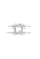
図1は、本発明の実施例のチューナブル高周波帯等分配回路を示す説明図である。
本実施例の帯等分配回路は、誘電体の下面にグランド層が形成された高周波回路基板の前記誘電体の上面に形成される。その高周波回路基板は、周知のものであるためここでは図示しない。帯等分配回路は、高周波回路基板の上面に設けられるマイクロストリップ線路と、そのマイクロストリップ線路に電気的に接続され、高周波を入出力する入出力線路と、を備えた高周波帯域等分配回路において、高周波の入力線路と出力線路に連なり動作周波数の2θ1の長さの線状の2つのマイクロストリップ線路と、その2つの線路の間に接続され動作周波数の2θ2の長さの線状の2つの副マイクロストリップ線路とから成り、2θ1と2θ2の4つのマイクロストリップ線路により略ロ字状に形成される。
FIG. 1 is an explanatory diagram showing a tunable high frequency band equal distribution circuit according to an embodiment of the present invention.
The band distribution circuit of this embodiment is formed on the upper surface of the dielectric of the high-frequency circuit board in which a ground layer is formed on the lower surface of the dielectric. Since the high-frequency circuit board is well known, it is not shown here. The band equal distribution circuit is a high frequency band equal distribution circuit comprising: a microstrip line provided on the upper surface of the high frequency circuit board; and an input / output line electrically connected to the microstrip line for inputting and outputting a high frequency. Two linear microstrip lines with an operating frequency of 2θ1 connected to a high-frequency input line and an output line, and two linear substrips with an operating frequency of 2θ2 connected between the two lines It consists of microstrip lines, and is formed in a substantially square shape by four microstrip lines 2θ1 and 2θ2.
マイクロストリップ線路の線路長θ1,θ2は、次式によって定められる。 The line lengths θ1 and θ2 of the microstrip line are determined by the following equations.
高周波を入出力する入出力線路は、マイクロストリップ線路の任意の位置にタップ接続する構成にしてもよい。高周波回路基板としては、PTFE、ガラスエポキシ、アルミナ、導体としては、銅箔が好適に利用できる。 The input / output line for inputting and outputting the high frequency may be configured to be tapped at an arbitrary position on the microstrip line. As the high-frequency circuit board, PTFE, glass epoxy, alumina, and copper foil can be suitably used as the conductor.
2つのマイクロストリップ線路の特性インピーダンスZは同一でもよいし、異なる値に設定してもよい。その特性インピーダンスZを、次式によって定められる。 The characteristic impedances Z of the two microstrip lines may be the same or may be set to different values. The characteristic impedance Z is determined by the following equation.
ただし、Z0は外部回路の特性インピーダンスである。 However, Z0 is the characteristic impedance of the external circuit.
入力線路との接続位置と出力線路との接続位置に、それぞれ容量性負荷Cを設け、その容量値により動作周波数の値を制御する。入出力線路との接続位置に設ける容量性負荷としては、容量の可変なチップキャパシタやバラクタダイオードが利用できる。
容量性負荷の容量値Cは、次式によって定められる。
Capacitive loads C are provided at the connection position with the input line and the connection position with the output line, respectively, and the value of the operating frequency is controlled by the capacitance value. As the capacitive load provided at the connection position with the input / output line, a variable-capacitance chip capacitor or varactor diode can be used.
The capacitance value C of the capacitive load is determined by the following equation.
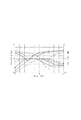
図2は、本発明の実施例のチューナブル高周波帯域等分配回路の特性を示すグラフである。
通過信号の中心周波数に2GHzを想定したものであり、S11は入力整合を示し、S21、S31は伝達特性を示し、S41はアイソレーションを示している。
FIG. 2 is a graph showing the characteristics of the tunable high frequency band equal distribution circuit according to the embodiment of the present invention.
It is assumed that the center frequency of the passing signal is 2 GHz, S11 indicates input matching, S21 and S31 indicate transfer characteristics, and S41 indicates isolation.
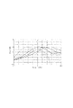
図3は、本発明によるチューナブル高周波帯等分配回路の実施例において、そのチューニングキャパシタCの値を変化させた場合の等分配周波数特性の変化を示すグラフである。
図示のように、チューニングキャパシタの容量値を変化させた場合、等分配値である3dBの値は変化しないが、動作周波数が変化することがわかる。
FIG. 3 is a graph showing the change of the equal distribution frequency characteristic when the value of the tuning capacitor C is changed in the embodiment of the tunable high frequency band equal distribution circuit according to the present invention.
As shown in the figure, when the capacitance value of the tuning capacitor is changed, the value of 3 dB which is the equally distributed value does not change, but the operating frequency changes.
本発明の高周波帯域等分配回路によると、製造容易で小型安価でありながらも安定した性能を有し、入力整合・アイソレーション・電力等分配・分配位相差90°を実現でき、また、動作周波数を任意に変化させられるので、特に、使用周波数が過密な周波数領域の各種移動体通信において、動作周波数を任意に選んで通信を行うコグニティブ無線やソフトウェア無線など、諸々の場面に活用でき、産業上利用価値が高い。 According to the high frequency band equal distribution circuit of the present invention, it is easy to manufacture, is small and inexpensive, and has stable performance, can realize input matching / isolation / power distribution / distribution phase difference of 90 °, and has an operating frequency. Can be used in various situations such as cognitive radio and software defined radio that perform communication by arbitrarily selecting the operating frequency, especially in various mobile communications in the frequency domain where the operating frequency is excessive. High utility value.
Claims (10)
入力線路との接続位置と出力線路との接続位置に、それぞれ動作周波数を制御する容量性負荷を設け、その容量値により動作周波数の値を制御する
ことを特徴とする高周波帯域等分配回路。 A high-frequency circuit board having a ground layer formed on the lower surface of the dielectric; a microstrip line provided on the upper surface of the high-frequency circuit board; In a high-frequency band equal distribution circuit comprising
A high-frequency band equal distribution circuit characterized in that a capacitive load for controlling the operating frequency is provided at each of the connection position with the input line and the connection position with the output line, and the value of the operating frequency is controlled by the capacitance value.
請求項1に記載の高周波帯域等分配回路。 A microstrip line is connected to a high-frequency input line and an output line and has two linear lines that have an approximate wavelength of the operating frequency, and two linear lines that are connected between the two lines and have an approximate wavelength of the operating frequency. The high frequency band equal distribution circuit according to claim 1, comprising a sub line.
請求項1または2に記載の高周波帯域等分配回路。 The high frequency band equal distribution circuit according to claim 1 or 2, wherein the two microstrip lines have the same characteristic impedance.
請求項1または2に記載の高周波帯域等分配回路。 The high frequency band equal distribution circuit according to claim 1 or 2, wherein the two microstrip lines have different characteristic impedances.
請求項1ないし4のいずれかに記載の高周波帯域等分配回路。 The high frequency band equal distribution circuit according to any one of claims 1 to 4, wherein the capacitive load provided at the connection position with the input / output line is a chip capacitor having a variable capacitance.
請求項1ないし4のいずれかに記載の高周波帯域等分配回路。 The high-frequency band equal distribution circuit according to any one of claims 1 to 4, wherein the capacitive load provided at the connection position with the input / output line is a varactor diode having a variable capacitance.
請求項1ないし6のいずれかに記載の高周波帯域等分配回路。 The high frequency band equal distribution circuit according to any one of claims 1 to 6, wherein an input / output line for inputting and outputting a high frequency is tapped to an arbitrary position of the microstrip line.
請求項1ないし7のいずれかに記載の高周波帯域等分配回路。 The line length θ1, θ2 of the microstrip line is
によって定める
請求項1ないし8のいずれかに記載の高周波帯域等分配回路。 The characteristic impedance Z of the microstrip line is
The high frequency band equal distribution circuit according to claim 1, defined by:
請求項1ないし9のいずれかに記載の高周波帯域等分配回路。
The capacitance value C of the capacitive load is
Priority Applications (1)
| Application Number | Priority Date | Filing Date | Title |
|---|---|---|---|
| JP2010272329A JP2012124635A (en) | 2010-12-07 | 2010-12-07 | High-frequency band equipartition circuit |
Applications Claiming Priority (1)
| Application Number | Priority Date | Filing Date | Title |
|---|---|---|---|
| JP2010272329A JP2012124635A (en) | 2010-12-07 | 2010-12-07 | High-frequency band equipartition circuit |
Publications (1)
| Publication Number | Publication Date |
|---|---|
| JP2012124635A true JP2012124635A (en) | 2012-06-28 |
Family
ID=46505648
Family Applications (1)
| Application Number | Title | Priority Date | Filing Date |
|---|---|---|---|
| JP2010272329A Pending JP2012124635A (en) | 2010-12-07 | 2010-12-07 | High-frequency band equipartition circuit |
Country Status (1)
| Country | Link |
|---|---|
| JP (1) | JP2012124635A (en) |
Citations (2)
| Publication number | Priority date | Publication date | Assignee | Title |
|---|---|---|---|---|
| JPH06216687A (en) * | 1993-01-18 | 1994-08-05 | Nippon Telegr & Teleph Corp <Ntt> | Variable frequency directional coupler |
| JP2003023310A (en) * | 2001-07-06 | 2003-01-24 | Hitachi Kokusai Electric Inc | Power distribution circuit and power combining circuit |
-
2010
- 2010-12-07 JP JP2010272329A patent/JP2012124635A/en active Pending
Patent Citations (2)
| Publication number | Priority date | Publication date | Assignee | Title |
|---|---|---|---|---|
| JPH06216687A (en) * | 1993-01-18 | 1994-08-05 | Nippon Telegr & Teleph Corp <Ntt> | Variable frequency directional coupler |
| JP2003023310A (en) * | 2001-07-06 | 2003-01-24 | Hitachi Kokusai Electric Inc | Power distribution circuit and power combining circuit |
Similar Documents
| Publication | Publication Date | Title |
|---|---|---|
| Deng et al. | A reconfigurable filtering antenna with integrated bandpass filters for UWB/WLAN applications | |
| JP4552205B2 (en) | Filter with switch function | |
| JP5218646B2 (en) | Variable capacity module and matching circuit module | |
| JP5928433B2 (en) | High frequency circuit module | |
| EP2096904A1 (en) | System for interconnecting two substrates each comprising at least one transmission line | |
| US8299869B2 (en) | Setting of a balun | |
| Chi et al. | Highly reconfigurable quadrature coupler with ideal impedance matching and port isolation | |
| JP2014112824A (en) | Antenna device | |
| US9059497B2 (en) | Variable filter and communication apparatus | |
| CN104966880A (en) | LTCC Wilkinson power divider with new structure | |
| CN104037477A (en) | Multi-band tunable microstrip band-pass filter | |
| JP4762920B2 (en) | Distribution circuit | |
| CN104716408B (en) | A kind of continuously variable type substrate integration wave-guide analog phase shifter | |
| US7633358B2 (en) | Phase shifter circuit with proper broadband performance | |
| Guermal et al. | A novel configuration of reconfigurable bandpass filter based on varactor diodes | |
| CN106207335A (en) | A kind of adjustable reconfigurable band filter | |
| CN106450601A (en) | Coupling control-based LTCC filtering switch | |
| CN201387935Y (en) | PIFA built-in antenna device | |
| Wong et al. | Impedance tuner using BST varactors in alumina-based IPD technology | |
| JP2012124635A (en) | High-frequency band equipartition circuit | |
| JP6502684B2 (en) | Filter element and communication module | |
| JP2012039473A (en) | Impedance variable matching circuit | |
| JP2008017159A (en) | Transmission line type lumped constant Wilkinson divider with two types of phase shifters | |
| Figur et al. | RF MEMS variable matching networks for multi-band and multi-mode GaN power amplifiers | |
| JP5682888B2 (en) | Tunable high frequency bandpass filter |
Legal Events
| Date | Code | Title | Description |
|---|---|---|---|
| A621 | Written request for application examination |
Free format text: JAPANESE INTERMEDIATE CODE: A621 Effective date: 20131007 |
|
| A521 | Written amendment |
Free format text: JAPANESE INTERMEDIATE CODE: A821 Effective date: 20131008 |
|
| A521 | Written amendment |
Free format text: JAPANESE INTERMEDIATE CODE: A523 Effective date: 20131202 |
|
| A521 | Written amendment |
Free format text: JAPANESE INTERMEDIATE CODE: A523 Effective date: 20140120 |
|
| A977 | Report on retrieval |
Free format text: JAPANESE INTERMEDIATE CODE: A971007 Effective date: 20140709 |
|
| A02 | Decision of refusal |
Free format text: JAPANESE INTERMEDIATE CODE: A02 Effective date: 20150507 |