JP2012103367A - Charging member, process cartridge and electrophotographic device - Google Patents
Charging member, process cartridge and electrophotographic device Download PDFInfo
- Publication number
- JP2012103367A JP2012103367A JP2010250152A JP2010250152A JP2012103367A JP 2012103367 A JP2012103367 A JP 2012103367A JP 2010250152 A JP2010250152 A JP 2010250152A JP 2010250152 A JP2010250152 A JP 2010250152A JP 2012103367 A JP2012103367 A JP 2012103367A
- Authority
- JP
- Japan
- Prior art keywords
- group
- formula
- carbon atoms
- compound
- represented
- Prior art date
- Legal status (The legal status is an assumption and is not a legal conclusion. Google has not performed a legal analysis and makes no representation as to the accuracy of the status listed.)
- Withdrawn
Links
Images


Abstract
Description
本発明は、電子写真感光体の表面を所定の電位に帯電するための帯電部材に関する。 The present invention relates to a charging member for charging the surface of an electrophotographic photosensitive member to a predetermined potential.
電子写真装置において、電子写真感光体(以下、単に「感光体」ということもある)、の表面を帯電する方式として、感光体の表面に接触して配置されたローラ形状の帯電部材(以降、帯電ローラともいう)を用いる接触帯電方式が多く採用されている。通常、帯電ローラは、感光体との接触部分の面積を大きくするため、導電性の弾性層と、表面保護のための導電性の表面層とを有する構成が一般的である。 In an electrophotographic apparatus, as a method of charging the surface of an electrophotographic photosensitive member (hereinafter, also simply referred to as “photosensitive member”), a roller-shaped charging member (hereinafter referred to as “contacting member”) disposed in contact with the surface of the photosensitive member. A contact charging method using a charging roller) is often used. Usually, the charging roller generally has a configuration having a conductive elastic layer and a conductive surface layer for surface protection in order to increase the area of the contact portion with the photoreceptor.
ところで、導電性粒子を含有させることによって導電化してなる表面層を有する帯電部材は、長期に亘って電圧が印加された状態が続くにつれて、帯電部材の電気抵抗値が徐々に変化してくることがある。特に低温低湿環境下では、その傾向が著しい。 By the way, in the charging member having a surface layer made conductive by containing conductive particles, the electric resistance value of the charging member gradually changes as the voltage is applied for a long time. There is. This tendency is particularly remarkable in a low temperature and low humidity environment.
より具体的には、帯電部材に電圧を印加し続けていると、部分的に電気抵抗が上昇し、当該部分の帯電性能が低下し、それに伴い、感光体の表面の帯電電位にムラが生じることがある。このような帯電電位のムラは、電子写真画像上にも反映されてしまうことがある。このような課題に対し、特許文献1には、導電性粒子の表面をカップリング剤で処理するという技術が開示されている。
More specifically, when a voltage is continuously applied to the charging member, the electrical resistance partially increases, the charging performance of the part decreases, and accordingly, the charged potential on the surface of the photosensitive member becomes uneven. Sometimes. Such unevenness of the charged potential may be reflected on the electrophotographic image. For such a problem,
しかしながら、本発明者らの検討によれば、カップリング剤で表面処理した導電性粒子を含有する導電性の表面層を備えた帯電部材であっても、過酷な条件、例えば、低温低湿環境下で、帯電部材に直流電圧を長期間印加したよな場合には、電気抵抗の経時的な変動が認められた。
そこで、本発明の目的は、過酷な条件下であっても電気抵抗の変動を、より一層抑制することのできる帯電部材の提供にある。
However, according to the study by the present inventors, even a charging member having a conductive surface layer containing conductive particles surface-treated with a coupling agent can be used under harsh conditions such as low temperature and low humidity. In the case where a DC voltage was applied to the charging member for a long period of time, a change in electric resistance with time was recognized.
Therefore, an object of the present invention is to provide a charging member that can further suppress fluctuations in electrical resistance even under severe conditions.
本発明によれば、導電性基体および表面層を有する帯電部材であって、該表面層は、バインダー樹脂と、導電性粒子の表面が、下記式(1)で示すユニットを有する化合物で被覆されている導電性複合粒子とを含有する帯電部材が提供される:
X2は、水素原子、炭素原子数1以上10以下のアルキル基、メチル基およびエチル基から選ばれる少なくとも一方で置換されていてもよいフェニル基、アリル基、ビニル基、上記式(18)で表わされる基および上記式(19)で表わされる基からなる群から選ばれる基である。上記式(3)においてXが下記式(19)である場合、式(19)で表わされる基の繰り返しの数は1以上10以下であり、かつ、最末端を構成している式(19)中のX2は、水素原子、炭素原子数1以上10以下のアルキル基、メチル基およびエチル基から選ばれる少なくとも一方で置換されていてもよいフェニル基、アリル基、ビニル基または上記式(18)で示される基である。)
X2 represents a hydrogen atom, an alkyl group having 1 to 10 carbon atoms, a phenyl group, an allyl group, a vinyl group which may be substituted at least one selected from a methyl group and an ethyl group, represented by the above formula (18). And a group selected from the group consisting of groups represented by the above formula (19). In the formula (3), when X is the following formula (19), the number of repeating groups represented by the formula (19) is 1 or more and 10 or less, and the most terminal formula (19) X2 therein is a hydrogen atom, an alkyl group having 1 to 10 carbon atoms, a phenyl group, an allyl group, a vinyl group which may be substituted at least one selected from a methyl group and an ethyl group, or the above formula (18) It is group shown by these. )
本発明によれば、表面層中の導電性粒子がバインダー中に固定化され、長期間の直流電圧の印加によっても表面層中の導電性粒子の移動が抑制される。その結果、帯電性能が長期に亘って安定した帯電部材を得ることができる。 According to the present invention, the conductive particles in the surface layer are fixed in the binder, and the movement of the conductive particles in the surface layer is suppressed even by applying a DC voltage for a long time. As a result, it is possible to obtain a charging member whose charging performance is stable over a long period of time.
本発明者らは、鋭意検討した結果、帯電部材の表面層に添加する導電性粒子を、後述する式(1)で示される構造を有する化合物を含有する物質で被覆した導電性複合粒子を使用することにより、長寿命化を達成できる帯電部材が得られることがわかった。
すなわち、本発明者らは、表面層の経時的な電気抵抗の変化は、表面層に添加している導電性粒子の酸化や、帯電部材の繰り返しの使用に伴う表面層の伸縮によって表面層中の導電性粒子の存在位置の変化による導電パスの切断などによるものと推測している。
一方、導電性粒子を被覆している、式(1)に係る化合物は非常にバルキーな構造を有するため、複合導電性粒子は、酸化されにくいものと考えられる。
As a result of intensive studies, the present inventors use conductive composite particles in which conductive particles added to the surface layer of the charging member are coated with a substance containing a compound having a structure represented by the formula (1) described later. By doing so, it was found that a charging member capable of achieving a long life can be obtained.
That is, the present inventors have found that the change in electrical resistance of the surface layer over time is caused by the oxidation of the conductive particles added to the surface layer and the expansion and contraction of the surface layer accompanying repeated use of the charging member. It is presumed that this is due to the cutting of the conductive path due to the change in the location of the conductive particles.
On the other hand, since the compound according to the formula (1) covering the conductive particles has a very bulky structure, the composite conductive particles are considered to be hardly oxidized.
また、当該化合物は、ビニル基またはビニル重合体の側鎖に、シロキサンデンドリマー構造(ポリシロキサン構造を核とし、シロキサン結合とシルアルキレン結合が交互に配列した高分岐構造)を備えた非常にバルキーな構造を有している。このような構造により、複合導電性粒子とバインダーとがよく絡み合い、表面層中での複合導電性粒子の位置が固定化される。表面層の繰り返しの伸縮や電圧印加によっても導電性粒子の移動が抑制されているものと考えられる。これらの理由により、本発明に係る帯電部材は、多様な環境の下での繰り返しの使用によっても、その帯電性能が経時的に変化し難くなっているものと考えられる。 In addition, the compound has a siloxane dendrimer structure (a highly branched structure in which a siloxane bond and a silalkylene bond are alternately arranged) in a vinyl group or a side chain of a vinyl polymer. It has a structure. With such a structure, the composite conductive particles and the binder are intertwined well, and the position of the composite conductive particles in the surface layer is fixed. It is considered that the movement of the conductive particles is suppressed by repeated expansion and contraction of the surface layer and voltage application. For these reasons, it is considered that the charging performance of the charging member according to the present invention does not easily change over time even after repeated use under various environments.
<帯電部材の構成>
本発明の帯電部材は、少なくとも導電性基体と、導電性基体上に設けられた表面層とを有する構成をなすものである。
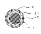
図1から図3に本発明の帯電部材の一例としての概略断面図を示す。図1は導電性基体1上に弾性層2を設け、更にその上に表面層3を設けたローラ形状の帯電部材(帯電ローラ)である。図2は弾性層2と表面層3との間に、中間層21を有する帯電ローラである。また、図3は弾性層2と表面層3との間に第1の中間層21および第2の中間層22を有する帯電ローラである。
<Configuration of charging member>
The charging member of the present invention comprises at least a conductive substrate and a surface layer provided on the conductive substrate.
1 to 3 show schematic sectional views as an example of the charging member of the present invention. FIG. 1 shows a roller-shaped charging member (charging roller) in which an elastic layer 2 is provided on a
<表面層の構成>
本発明に係る表面層は、バインダーと、導電性粒子を下記式(1)で示すユニットを有する化合物を含有する物質で被覆した導電性複合粒子とを含有する。
The surface layer according to the present invention contains a binder and conductive composite particles obtained by coating the conductive particles with a substance containing a compound having a unit represented by the following formula (1).
<式(1)で示すユニットを有する化合物>
前記式(1)で示すユニットを有する化合物は、ビニル基、もしくは、ビニル重合体の側鎖に、シロキサンデンドリマー構造(ポリシロキサン構造を核とし、シロキサン結合とシルアルキレン結合が交互に配列した高分岐構造)を有する。
前記式(1)で示されるR1は、水素原子や、メチル基、エチル基、プロピル基、イソプロピル基およびブチル基のような炭素原子数1以上4以下のアルキル基が例示される。Gは式(2)で表わされる構造を有する基である。
<Compound having unit represented by formula (1)>
The compound having the unit represented by the formula (1) is a highly branched group in which a vinyl group or a side chain of a vinyl polymer has a siloxane dendrimer structure (a polysiloxane structure is a nucleus, and siloxane bonds and silalkylene bonds are alternately arranged. Structure).
Examples of R1 represented by the formula (1) include a hydrogen atom and an alkyl group having 1 to 4 carbon atoms such as a methyl group, an ethyl group, a propyl group, an isopropyl group, and a butyl group. G is a group having a structure represented by the formula (2).
(式(1)中、R1は水素原子または炭素原子数1以上4以下のアルキル基である。Gは式(2)で表わされる構造を有する基である。)
本構造とすることにより、導電性粒子を被覆した際の化合物の安定性を更に高めることが可能になる。 By adopting this structure, it becomes possible to further improve the stability of the compound when the conductive particles are coated.
R8およびR9は、メチレン基、エチレン基、プロピレン基、ブチレン基のようなアルキレン基が例示され、この中でも、メチレン基、プロピレン基がより好ましい。
R10は、メチル基、エチル基、プロピル基、ブチル基のようなアルキル基が例示され、これらの中でもメチル基がより好ましい。R11は、メチレン基、エチレン基、プロピレン基、ブチレン基のようなアルキレン基が例示され、これらの中でもエチレン基がより好ましい。
R8 and R9 are exemplified by an alkylene group such as a methylene group, an ethylene group, a propylene group, and a butylene group, and among them, a methylene group and a propylene group are more preferable.
R10 is exemplified by an alkyl group such as a methyl group, an ethyl group, a propyl group, and a butyl group, and among these, a methyl group is more preferable. R11 is exemplified by an alkylene group such as a methylene group, an ethylene group, a propylene group, and a butylene group, and among these, an ethylene group is more preferable.
式(2)で示すE1、E2およびE3は、各々独立に下記式(3)で表わされる基である。また、aは0または1である。 E1, E2 and E3 represented by the formula (2) are each independently a group represented by the following formula (3). A is 0 or 1.
式(3)で示すZ1は、炭素原子数2以上10以下のアルキレン基、メチル基およびエチル基から選ばれる少なくとも一方で置換されていてもよいフェニレン基、下記式(15)〜式(17)で示される基であり、エチレン基、プロピレン基、ブチレン基、ヘキシレン基のような直鎖状アルキレン基、メチルメチレン基、メチルエチレン基、1−メチルペンチレン基、1,4−ジメチルブチレン基のような分岐状アルキレン基が例示される。また、式(3)で示すkは0または1であり、hは0以上3以下の整数である。 Z1 represented by formula (3) is an alkylene group having 2 to 10 carbon atoms, a phenylene group optionally substituted from at least one selected from a methyl group and an ethyl group, and the following formulas (15) to (17): A linear alkylene group such as ethylene group, propylene group, butylene group, hexylene group, methylmethylene group, methylethylene group, 1-methylpentylene group, 1,4-dimethylbutylene group Such branched alkylene groups are exemplified. Moreover, k shown by Formula (3) is 0 or 1, and h is an integer of 0 or more and 3 or less.
R3、R4、R6およびR7は各々独立に炭素原子数1以上5以下のアルキル基またはメチル基およびエチル基から選ばれる少なくとも一方で置換されていてもよいフェニル基である。
R5は炭素原子数1以上10以下のアルコキシ基、メチル基およびエチル基から選ばれる少なくとも一方で置換されていてもよいフェノキシ基、下記式(20)または下記式(21)で示される基である。
Xは、水素原子、炭素原子数1以上10以下のアルキル基、メチル基およびエチル基から選ばれる少なくとも一方で置換されていてもよいフェニル基、アリル基、ビニル基、下記式(18)で表わされる基および下記式(19)で表わされる基からなる群から選ばれる基である。
R5 is a group represented by the following formula (20) or the following formula (21) optionally substituted by at least one selected from an alkoxy group having 1 to 10 carbon atoms, a methyl group and an ethyl group. .
X represents a hydrogen atom, an alkyl group having 1 to 10 carbon atoms, a phenyl group, an allyl group, a vinyl group which may be substituted at least one selected from a methyl group and an ethyl group, represented by the following formula (18). And a group selected from the group consisting of groups represented by the following formula (19).
前記式(3)においてR3、R4、R6およびR7は、各々独立に、炭素原子数1以上5以下のアルキル基またはフェニル基である。これらの中でもメチル基が更に好ましい。 In the formula (3), R3, R4, R6 and R7 are each independently an alkyl group having 1 to 5 carbon atoms or a phenyl group. Among these, a methyl group is more preferable.
R5は炭素原子数1以上10以下のアルコキシ基、メチル基およびエチル基から選ばれる少なくとも一方で置換されていてもよいフェノキシ基、下記式(20)または下記式(21)で示される基である。
Z2は炭素原子数2以上10以下のアルキレン基、メチル基およびエチル基から選ばれる少なくとも一方で置換されていてもよいフェニレン基および上記式(15)〜(17)で表わされる2価の基からなる群から選ばれる基を示す。R19、R20、R22およびR23は各々独立に炭素原子数1以上5以下のアルキル基またはメチル基およびエチル基から選ばれる少なくとも一方で置換されていてもよいフェニル基を示す。R21は炭素原子数1以上10以下のアルコキシ基、メチル基およびエチル基から選ばれる少なくとも一方で置換されていてもよいフェノキシ基、下記式(20)または下記式(21)で示される基である。
X2は、水素原子、炭素原子数1以上10以下のアルキル基、メチル基およびエチル基から選ばれる少なくとも一方で置換されていてもよいフェニル基、アリル基、ビニル基、上記式(18)で表わされる基および上記式(19)で表わされる基からなる群から選ばれる基である。
上記式(3)においてXが下記式(19)である場合、式(19)で表わされる基の繰り返しの数は1以上10以下であり、かつ、最末端を構成している式(19)中のX2は、水素原子、炭素原子数1以上10以下のアルキル基、メチル基およびエチル基から選ばれる少なくとも一方で置換されていてもよいフェニル基、アリル基、ビニル基または上記式(18)で示される基である。
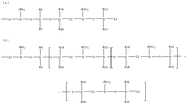
ここで、式(3)において、k=0であって、Xが式(19)であり、かつ、式(19)で表わされる基の繰り返しの数が1であるときの式(3)の構造を図8(a)に示す。また、当該繰り返しの数が3であるときの式(3)の構造を図8(b)に示す。
Z2 is an alkylene group having 2 to 10 carbon atoms, a phenylene group which may be substituted at least one selected from a methyl group and an ethyl group, and a divalent group represented by the above formulas (15) to (17). A group selected from the group consisting of: R19, R20, R22 and R23 each independently represents an alkyl group having 1 to 5 carbon atoms or a phenyl group which may be substituted at least one selected from a methyl group and an ethyl group. R21 is a group represented by the following formula (20) or the following formula (21) optionally substituted by at least one selected from an alkoxy group having 1 to 10 carbon atoms, a methyl group and an ethyl group. .
X2 represents a hydrogen atom, an alkyl group having 1 to 10 carbon atoms, a phenyl group, an allyl group, a vinyl group which may be substituted at least one selected from a methyl group and an ethyl group, represented by the above formula (18). And a group selected from the group consisting of groups represented by the above formula (19).
In the formula (3), when X is the following formula (19), the number of repeating groups represented by the formula (19) is 1 or more and 10 or less, and the most terminal formula (19) X2 therein is a hydrogen atom, an alkyl group having 1 to 10 carbon atoms, a phenyl group, an allyl group, a vinyl group which may be substituted at least one selected from a methyl group and an ethyl group, or the above formula (18) It is group shown by these.
Here, in the formula (3), k = 0, X is the formula (19), and the number of repetitions of the group represented by the formula (19) is 1, The structure is shown in FIG. FIG. 8B shows the structure of the formula (3) when the number of repetitions is 3.
尚、前記式(3)〜(21)中の、各々の基は、E1、E2およびE3おいて、前記定義を満たしていれば、異なる基であってもよい。例えば、E1を構成する前記式(3)中のZ1と、E2を構成する前記式(3)中のZ1は、炭素原子数2以上10以下のアルキレン基、メチル基およびエチル基から選ばれる少なくとも一方で置換されていてもよいフェニレン基および下記式(15)〜(17)で表わされる2価の基からなる群から選ばれる基であれば、異なっていてもよい。 In addition, each group in said Formula (3)-(21) may be different groups, as long as the said definition is satisfied in E1, E2, and E3. For example, Z1 in the formula (3) constituting E1 and Z1 in the formula (3) constituting E2 are at least selected from an alkylene group having 2 to 10 carbon atoms, a methyl group, and an ethyl group. On the other hand, it may be different as long as it is a group selected from the group consisting of an optionally substituted phenylene group and a divalent group represented by the following formulas (15) to (17).
前記式(3)中のhが0であり、Xが前記式(19)で表わされる基であって、式(19)で表わされる基の繰り返しの数が1以上3以下であり、かつ、前記式(19)中のrが0であることが更に好ましい。これらにより、化合物の撥水性を更に向上させることができ、導電性粒子の吸湿を更に抑制できる。 H in the formula (3) is 0, X is a group represented by the formula (19), and the number of repeating groups represented by the formula (19) is 1 or more and 3 or less, and More preferably, r in the formula (19) is 0. By these, the water repellency of a compound can further be improved and the moisture absorption of electroconductive particle can further be suppressed.
前記化合物は、前記式(1)で示すユニットを有すると共に、更に下記式(4)で示すユニットを有することが、より好ましい。
式(4)において、R2としては、水素原子、または、メチル基、エチル基、プロピル基、イソプロピル基およびブチル基のような炭素原子数1以上4以下のアルキル基が例示される。 In the formula (4), examples of R2 include a hydrogen atom or an alkyl group having 1 to 4 carbon atoms such as a methyl group, an ethyl group, a propyl group, an isopropyl group, and a butyl group.
Jは、水素原子、炭素原子数1以上4以下のアルキル基、メチル基およびエチル基から選ばれる少なくとも一方で置換されていてもよいフェニル基、下記式(9)、(10)、または(11)で示される基である。 J is a hydrogen atom, an alkyl group having 1 to 4 carbon atoms, a phenyl group which may be substituted at least one selected from a methyl group and an ethyl group, the following formulas (9), (10) or (11 ).
この中でも、下記式(9)、(10)または(11)で示される構造であることがより好ましい。
前記式(4)に示すようなビニル重合体との共重合体のような構造を有することにより、導電性粒子表面を被覆させやすく、また、一旦被覆したものが剥離しにくくなり、導電性粒子への吸湿やその表面の酸化を抑制する効果が更に強くなる。また、表面層のバインダー樹脂との絡み合いをより強固にし、導電性粒子に電荷が加わった際の導電性粒子の僅かな移動が抑制され、結果的に長時間電圧を印加し続けても通電による劣化の非常に少ない帯電部材を得ることが可能となる。 By having a structure like a copolymer with a vinyl polymer as shown in the above formula (4), it is easy to coat the surface of the conductive particles, and once coated, it becomes difficult to peel off. The effect of suppressing moisture absorption and oxidation on the surface is further enhanced. In addition, the entanglement with the binder resin of the surface layer is further strengthened, and the slight movement of the conductive particles when electric charges are applied to the conductive particles is suppressed. As a result, even if a voltage is continuously applied for a long time, It becomes possible to obtain a charging member with very little deterioration.
本発明の化合物の分子量はポリスチレン換算の数平均分子量で、10000以上のものを指し、より好ましくは20000以上2000000以下の範囲である。分子量が10000以上の場合、導電性粒子を十分に被覆することができ、好ましい。 The molecular weight of the compound of the present invention is a polystyrene-equivalent number average molecular weight of 10,000 or more, more preferably in the range of 20,000 to 2,000,000. When the molecular weight is 10,000 or more, the conductive particles can be sufficiently covered, which is preferable.
前記化合物は、下記式(12)で示す化合物、もしくは、下記式(12)を重合することにより得ることができる。
式(12)で示す構造の一例を、式(13)および式(14)に示す。
更に、前記化合物は、式(12)に示す化合物と、ビニル基を有する化合物を重合反応させることにより得ることができる。 Furthermore, the compound can be obtained by polymerizing a compound represented by the formula (12) and a compound having a vinyl group.
ビニル基を有する化合物としては、ラジカル重合性のビニル基を有するものであればよい。中でも、低級アルキル(メタ)アクリレート、芳香族ビニル型単量体およびアミド基含有ビニル型単量体がより好ましい。具体的には、低級アルキル(メタ)アクリレートとしては、(メタ)アクリル酸メチル、(メタ)アクリル酸エチル、(メタ)アクリル酸プロピル、(メタ)アクリル酸ブチルが例示できる。芳香族ビニル型単量体としては、スチレン、ビニルトルエン、ベンジル(メタ)アクリレート、フェノキシエチル(メタ)アクリレートが例示できる。アミド基含有ビニル型単量体としては、(メタ)アクリルアミド、N−メチロール(メタ)アクリルアミド、N−メトキシメチル(メタ)アクリルアミド、N,N−ジメチル(メタ)アクリルアミドが例示できる。 The compound having a vinyl group may be any compound having a radical polymerizable vinyl group. Of these, lower alkyl (meth) acrylates, aromatic vinyl monomers and amide group-containing vinyl monomers are more preferred. Specifically, examples of the lower alkyl (meth) acrylate include methyl (meth) acrylate, ethyl (meth) acrylate, propyl (meth) acrylate, and butyl (meth) acrylate. Examples of the aromatic vinyl type monomer include styrene, vinyl toluene, benzyl (meth) acrylate, and phenoxyethyl (meth) acrylate. Examples of the amide group-containing vinyl monomer include (meth) acrylamide, N-methylol (meth) acrylamide, N-methoxymethyl (meth) acrylamide, and N, N-dimethyl (meth) acrylamide.
また、前記式(12)で示す化合物と、上記ビニル基を有する化合物との混合比率を調整することにより、前記化合物全体に対し、前記式(1)で示すユニットの含有量を調整することができる。 Further, by adjusting the mixing ratio of the compound represented by the formula (12) and the compound having a vinyl group, the content of the unit represented by the formula (1) can be adjusted with respect to the entire compound. it can.
前記化合物を得るための重合法としては、ラジカル重合法やイオン重合法が使用される。この中でも、ラジカル重合法がより好ましく、ラジカル重合法の中でも、溶液重合法が更に好ましい。 As a polymerization method for obtaining the compound, a radical polymerization method or an ionic polymerization method is used. Among these, the radical polymerization method is more preferable, and among the radical polymerization methods, the solution polymerization method is more preferable.
溶液重合法は、溶媒中で、前記式(12)で示す化合物のみ、あるいは、前記式(12)で示す化合物とビニル基を有する化合物とをラジカル開始剤の存在下、50℃以上150℃以下の温度条件下で反応させることにより行われる。 In the solution polymerization method, only a compound represented by the formula (12) or a compound represented by the formula (12) and a compound having a vinyl group are mixed in a solvent in the presence of a radical initiator at 50 ° C. or higher and 150 ° C. or lower. The reaction is carried out under the following temperature conditions.
このとき用いる溶媒としては、ヘキサン、オクタン、デカン、シクロヘキサンのような脂肪族炭化水素等を例示できる。 Examples of the solvent used at this time include aliphatic hydrocarbons such as hexane, octane, decane, and cyclohexane.
ラジカル開始剤としては、一般にラジカル重合法に使用される従来公知の化合物が用いられ、具体的には、2,2´−アゾビス(イソブチロニトリル)、2,2´−アゾビス(2−メチルブチロニトリル)、2,2´−アゾビス(2,4−ジメチルバレロニトリル)のようなアゾビス系化合物、過酸化ベンゾイル、過酸化ラウロイル、tert−ブチルパーオキシベンゾエート、tert−ブチルパーオキシ−2−エチルヘキサノエートのような有機過酸化物を例示できる。
このラジカル開始剤は、1種を単独で使用してもよく、また2種類以上を混合して使用してもよい。ラジカル開始剤の使用量は、重合する化合物の合計を100質量部としたとき、0.1質量部以上5質量部以下の範囲であることが好ましい。
As the radical initiator, conventionally known compounds generally used in radical polymerization methods are used. Specifically, 2,2′-azobis (isobutyronitrile), 2,2′-azobis (2-methyl) are used. Butyronitrile), azobis compounds such as 2,2'-azobis (2,4-dimethylvaleronitrile), benzoyl peroxide, lauroyl peroxide, tert-butylperoxybenzoate, tert-butylperoxy-2- An organic peroxide such as ethylhexanoate can be exemplified.
This radical initiator may be used individually by 1 type, and may mix and use 2 or more types. The amount of radical initiator used is preferably in the range of 0.1 parts by mass or more and 5 parts by mass or less when the total amount of the compounds to be polymerized is 100 parts by mass.
また、重合に際しては連鎖移動剤を添加することができる。この連鎖移動剤の具体的を以下に挙げる。2−メルカプトエタノール、ブチルメルカプタン、n−ドデシルメルカプタン、3−メルカプトプロピルトリメトキシシラン、メルカプトプロピル基を有するポリジメチルシロキサンのようなメルカプト化合物等。
このような連鎖移動剤の配合量は、重合する化合物の合計を100質量部としたとき、好ましくは、0.001質量部以上15質量部以下、さらに好ましくは、0.01質量部以上10質量部以下である。なお、本発明の重合体を製造する場合、重合後、加熱下、減圧処理して、残存する未反応のビニル系化合物を除去することが好ましい。
A chain transfer agent can be added during the polymerization. Specific examples of this chain transfer agent are listed below. Mercapto compounds such as 2-mercaptoethanol, butyl mercaptan, n-dodecyl mercaptan, 3-mercaptopropyltrimethoxysilane, and polydimethylsiloxane having a mercaptopropyl group.
The amount of such chain transfer agent is preferably 0.001 to 15 parts by mass, more preferably 0.01 to 10 parts by mass, when the total amount of the compounds to be polymerized is 100 parts by mass. Or less. In addition, when manufacturing the polymer of this invention, it is preferable to remove the unreacted vinyl-type compound which remain | survives by carrying out pressure reduction treatment under a heating after superposition | polymerization.
<導電性粒子を被覆する前記式(1)で示すユニットを有する化合物を含有する物質>
本発明において、導電性粒子を被覆する物質として、少なくとも前記式(1)で示すユニットを有する化合物を含有していればよいが、好ましくは50%以上含有していることが好ましく。より好ましくは80%以上含有していることが好ましい。
<Material containing a compound having a unit represented by the formula (1) that coats conductive particles>
In the present invention, the substance covering the conductive particles may contain at least a compound having a unit represented by the formula (1), but preferably contains 50% or more. More preferably, it contains 80% or more.
<導電性粒子>
導電性粒子としては電子導電性粒子やイオン導電性粒子を用い得る。
<Conductive particles>
As the conductive particles, electron conductive particles or ion conductive particles can be used.
電子導電性粒子としては、アルミニウム、パラジウム、鉄、銅、銀の如き金属系の微粒子や、酸化チタン、酸化錫、酸化亜鉛、酸化ケイ素の如き金属酸化物およびこれらに異種金属、異種金属酸化物のような物質をドープした金属酸化物、前記記載の金属系の微粒子、および金属酸化物の表面に、電解処理、スプレー塗工、混合振とうにより表面処理した複合粒子、ファーネスブラック、サーマルブラック、アセチレンブラック、ケッチェンブラック、PAN(ポリアクリロニトリル)系カーボン、ピッチ系カーボンの如きカーボン粉が例示される。また、これらの電子導電性粒子を単独でまたは2種以上組み合わせて用いることができる。 Electroconductive particles include metal-based fine particles such as aluminum, palladium, iron, copper and silver, metal oxides such as titanium oxide, tin oxide, zinc oxide and silicon oxide, and different metals and different metal oxides. Metal oxides doped with such materials, metal-based fine particles as described above, and composite particles surface-treated by electrolytic treatment, spray coating, mixed shaking, furnace black, thermal black, Examples thereof include carbon powders such as acetylene black, ketjen black, PAN (polyacrylonitrile) -based carbon, and pitch-based carbon. These electronic conductive particles can be used alone or in combination of two or more.
イオン導電性粒子としては、以下に挙げる低分子イオン導電剤を、ポリエーテル結合を有する樹脂(例えば、ポリエチレンオキサイド、ポリプロピレンオキサイド、ポリエーテルアミド、ポリエーテルエステルアミド、ポリエーテルエステル)に練り込んだものが例示できる。
低分子イオン導電剤としては、過塩素酸リチウム、過塩素酸ナトリウム、過塩素酸カルシウムの如き無機イオン物質を例示することができる。
As ion conductive particles, the following low molecular ion conductive agents are kneaded into a resin having a polyether bond (for example, polyethylene oxide, polypropylene oxide, polyether amide, polyether ester amide, polyether ester). Can be illustrated.
Examples of the low molecular ion conductive agent include inorganic ionic substances such as lithium perchlorate, sodium perchlorate, and calcium perchlorate.
また、導電性粒子としては、上記の電子導電性粒子とイオン導電性粒子とを複合化したハイブリッド粒子も用いることができる。
このようなハイブリッド粒子の作製方法としては、予めポリエーテルエステルアミド、ポリエステルアミド、ポリエーテルアミド、ポリエーテルエステルのようなイオン導電性粒子に電子導電性粒子を混練し、ペレット状としたものを公知の方法(例えば、機械粉砕、冷凍粉砕)により粉砕し、必要に応じて分級を行って所望のハイブリッド粒子を得る。
また、より球状に近いハイブリッド粒子を得る方法としては、以下のような方法が挙げられる。予めポリエーテルエステルアミド、ポリエステルアミド、ポリエーテルアミド、ポリエーテルエステルのようなイオンに電子導電性粒子を混練した複合樹脂(これを複合樹脂Aとする)を複合樹脂Aと相溶性のない別の樹脂(これを樹脂Bとする)と混合し、複合樹脂Aと樹脂Bとを均一に混合・分散させる。その後、この混合物を融点以下に冷却し、複合樹脂Aとは非相溶だが、樹脂Bとは相溶する展開溶媒と上記樹脂混合物を混合して樹脂粒子の懸濁液とする。そして、これを遠心分離、濾過、またはこれらの方法を組み合わせて分離することにより、複合樹脂Aからなる粒子を得ることができる。樹脂Bとしては、例えば、ポリエチレンオキサイド、ポリエチレングリコール、ポリビニルアルコールが例示でき、これらを単独で、あるいは組み合わせたものが使用できる。
As the conductive particles, hybrid particles obtained by combining the above electronic conductive particles and ionic conductive particles can also be used.
As a method for producing such hybrid particles, a method in which electron conductive particles are previously kneaded with ion conductive particles such as polyether ester amide, polyester amide, polyether amide, and polyether ester to form a pellet is known. The desired hybrid particles are obtained by pulverization by the above method (for example, mechanical pulverization, freeze pulverization) and classification as necessary.
Moreover, the following methods are mentioned as a method of obtaining the hybrid particle nearer spherical. A composite resin (hereinafter referred to as composite resin A) in which electronic conductive particles are kneaded with ions such as polyether ester amide, polyester amide, polyether amide, and polyether ester in advance is not compatible with composite resin A. A resin (this is referred to as “resin B”) is mixed, and the composite resin A and the resin B are uniformly mixed and dispersed. Thereafter, the mixture is cooled to a temperature equal to or lower than the melting point, and a developing solvent which is incompatible with the composite resin A but is compatible with the resin B and the resin mixture are mixed to obtain a suspension of resin particles. And the particle | grains which consist of composite resin A can be obtained by isolate | separating this by centrifugation, filtration, or combining these methods. Examples of the resin B include polyethylene oxide, polyethylene glycol, and polyvinyl alcohol, and these can be used alone or in combination.
<導電性粒子の平均粒径>
導電性粒子の平均粒径の目安としては、30μm未満、特には、10μm未満である。
<Average particle size of conductive particles>
As a standard of the average particle diameter of the conductive particles, it is less than 30 μm, particularly less than 10 μm.
<導電性粒子の体積抵抗率>
また、導電性粒子の体積抵抗率の目安としては、106Ω・cm以下、特には、10−3Ω・cm以上103Ω・cm以下の範囲である。
<Volume resistivity of conductive particles>
The volume resistivity of the conductive particles is 10 6 Ω · cm or less, particularly 10 −3 Ω · cm or more and 10 3 Ω · cm or less.
<導電性粒子と化合物との比率>
導電性粒子と式(1)の化合物との比率の目安としては、導電性粒子の表面の全体を被覆するのに最低限の量の化合物があればよい。
<Ratio of conductive particles to compound>
As a measure of the ratio between the conductive particles and the compound of the formula (1), a minimum amount of the compound is sufficient to cover the entire surface of the conductive particles.
<化合物による導電性粒子の被覆方法>
本発明における化合物による導電性粒子の被覆方法としては、湿式による方法、乾式による方法が挙げられる。
<Method of coating conductive particles with compound>
Examples of the method for coating the conductive particles with the compound in the present invention include a wet method and a dry method.
湿式による方法は、詳細には、本発明の化合物を可溶な溶剤に溶解して、溶液とした後、この溶液を導電性粒子表面に塗布した後、溶剤を乾燥することによって得る方法が挙げられる。
より具体的には、導電性粒子を浮遊流動させながら、化合物の溶液をスプレーし、導電性粒子表面に化合物の被覆層を形成させる方法が挙げられる。このような装置として、ヘンシェルミキサー、プラネタリーミキサー、ナウターミキサー、マルチパーパスミキサーが挙げられる。
Specifically, the wet method includes a method obtained by dissolving the compound of the present invention in a soluble solvent to form a solution, applying the solution to the surface of the conductive particles, and then drying the solvent. It is done.
More specifically, a method of spraying a solution of the compound while floating and flowing the conductive particles to form a coating layer of the compound on the surface of the conductive particles can be mentioned. Examples of such an apparatus include a Henschel mixer, a planetary mixer, a nauter mixer, and a multipurpose mixer.
乾式による方法として、化合物の粒子と導電性粒子とを機械的に混合して被覆する方法、導電性粒子に化合物の粒子を機械的衝撃力により被覆する方法、化合物の粒子と導電性粒子とを機械的に混合した後に加熱することで導電性粒子を被覆する方法のような方法が挙げられる。
化合物の粒子と導電性粒子とを機械的に混合して被覆する装置としては、例えばメカノミル(岡田精工社製)、メカノフュ−ジョンシステム(ホソカワミクロン社製)、ペイントコンディショナー(レッドデビル社製)のような装置を使用することができる。
導電性粒子に化合物の粒子を機械的衝撃力により被覆する装置としては、例えばハイブリダイザ−(奈良機械製作所社製)のような装置を使用することができる。
また、加熱処理する装置としては、スピラコ−タ−(岡田精工社製)、サフュ−ジングシステム(日本ニュ−マチック社製)のような装置を使用することができる。
As a dry method, a method in which compound particles and conductive particles are mixed and coated mechanically, a method in which conductive particles are coated with compound particles by mechanical impact force, a compound particle and conductive particles Examples thereof include a method such as a method of coating conductive particles by heating after mechanical mixing.
As an apparatus for mechanically mixing and coating compound particles and conductive particles, for example, Mechano Mill (Okada Seiko Co., Ltd.), Mechano Fusion System (Hosokawa Micron Co., Ltd.), Paint Conditioner (Red Devil Co.) Equipment can be used.
An apparatus such as a hybridizer (manufactured by Nara Machinery Co., Ltd.) can be used as an apparatus for coating conductive particles with compound particles by mechanical impact force.
Moreover, as an apparatus to heat-process, apparatuses, such as a spiracoater (made by Okada Seiko Co., Ltd.) and a fusing system (made by Nippon Numatic Co., Ltd.) can be used.
<バインダー樹脂>
表面層に用いるバインダー樹脂としては、公知のバインダーを採用することができる。例えば、樹脂、天然ゴムやこれを加硫処理したもの、合成ゴムのようなゴムを挙げることができる。
樹脂としては、熱硬化性樹脂、熱可塑性樹脂のような樹脂が使用できる。中でも、フッ素樹脂、ポリアミド樹脂、アクリル樹脂、ポリウレタン樹脂、シリコーン樹脂、ブチラール樹脂がより好ましい。
合成ゴムとしては、エチレン−プロピレン−ジエン共重合体(EPDM)、スチレン−ブタジエン共重合ゴム(SBR)、シリコーンゴム、ウレタンゴム、イソプレンゴム(IR)、ブチルゴム、アクリロニトリル−ブタジエン共重合ゴム(NBR)、クロロプレンゴム(CR)、アクリルゴムおよびエピクロルヒドリンゴムが使用できる。
これらは、単独で用いてもよいし、2種以上を混合して用いても、また共重合体であってもよい。なお、これらの中でも、表面層に用いるバインダー樹脂としては、感光体やその他の部材を汚染せず離型性が高いという観点から、樹脂を用いることが好ましい。
<Binder resin>
As the binder resin used for the surface layer, a known binder can be employed. Examples thereof include resins, natural rubber, vulcanized products thereof, and rubbers such as synthetic rubber.
As the resin, a resin such as a thermosetting resin or a thermoplastic resin can be used. Among these, fluorine resin, polyamide resin, acrylic resin, polyurethane resin, silicone resin, and butyral resin are more preferable.
Synthetic rubbers include ethylene-propylene-diene copolymer (EPDM), styrene-butadiene copolymer rubber (SBR), silicone rubber, urethane rubber, isoprene rubber (IR), butyl rubber, acrylonitrile-butadiene copolymer rubber (NBR). Chloroprene rubber (CR), acrylic rubber and epichlorohydrin rubber can be used.
These may be used alone, in combination of two or more, or may be a copolymer. Among these, as the binder resin used for the surface layer, it is preferable to use a resin from the viewpoint of high releasability without contaminating the photoreceptor or other members.
<本発明の表面層に添加する他の粒子>
表面層には、本発明の効果を損なわない範囲で絶縁性粒子等を含有させてもよい。
<Other particles added to the surface layer of the present invention>
The surface layer may contain insulating particles or the like as long as the effects of the present invention are not impaired.
表面層には、表面の離型性を向上させるために、離型剤を含有させても良い。表面層に離型剤を含有させることで、帯電部材の表面に汚れが付着することを防ぎ、帯電部材の耐久性を向上させることができる。離型剤が液体の場合は、表面層を形成する際にレベリング剤としても作用する。
このような離型剤として、低表面エネルギーや摺動性のような物性を有する物質を利用することができ、その性状として、固体および液体のものを用いることができる。具体的には、二硫化モリブデン、二硫化タングステン、窒化ホウ素、一酸化鉛のような金属酸化物を挙げることができる。また、オイル状あるいは固体状(離型性樹脂あるいはその粉末、ポリマーの一部に離形性を有する部位を導入したもの)のケイ素やフッ素を分子内に含む化合物、ワックス、高級脂肪酸、その塩やエステル、その他誘導体も使用できる。
The surface layer may contain a release agent in order to improve the surface releasability. By including a release agent in the surface layer, it is possible to prevent dirt from adhering to the surface of the charging member and improve the durability of the charging member. When the release agent is a liquid, it also acts as a leveling agent when forming the surface layer.
As such a release agent, a substance having physical properties such as low surface energy and slidability can be used, and solid and liquid materials can be used as its properties. Specifically, metal oxides such as molybdenum disulfide, tungsten disulfide, boron nitride, and lead monoxide can be given. In addition, oil- or solid-state compounds (mold release resin or powder thereof, a part of the polymer with a part having a release property) silicon or fluorine in the molecule, wax, higher fatty acid, salt thereof , Esters and other derivatives can also be used.
<表面層の厚さ、その他処理>
表面層は、0.1μm以上100μm以下の厚さを有することが好ましい。より好ましくは、1μm以上50μm以下である。
なお、表面層の膜厚は、帯電ローラ断面を鋭利な刃物で切り出して、光学顕微鏡や電子顕微鏡で観察することで測定できる。
<Thickness of surface layer, other treatment>
The surface layer preferably has a thickness of 0.1 μm or more and 100 μm or less. More preferably, they are 1 micrometer or more and 50 micrometers or less.
The film thickness of the surface layer can be measured by cutting the charging roller section with a sharp blade and observing with an optical microscope or an electron microscope.
表面層は、表面処理が施されていてもよい。表面処理としては、UVや電子線を用いた表面加工処理や、化合物を表面に付着および/または含浸させる表面改質処理を挙げることができる。 The surface layer may be subjected to a surface treatment. Examples of the surface treatment include a surface processing treatment using UV or electron beam and a surface modification treatment for adhering and / or impregnating a compound on the surface.
<帯電部材の表面粗さ>
本発明の帯電部材は、表面の十点平均粗さRzjis(μm)が3≦Rzjis≦30であり、表面の凹凸平均間隔Rsm(μm)が15≦Rsm≦150であることがより好ましい。帯電部材の十点平均表面粗さRzjis、凹凸平均間隔Rsmをこの範囲とすることにより、帯電部材と電子写真感光体との接触状態をより安定にすることができる。これにより、感光体を均一に帯電することが容易になるため、より好ましい。
<Surface roughness of charging member>
In the charging member of the present invention, it is more preferable that the surface ten-point average roughness Rzjis (μm) is 3 ≦ Rzjis ≦ 30, and the surface unevenness average interval Rsm (μm) is 15 ≦ Rsm ≦ 150. By setting the ten-point average surface roughness Rzjis and the uneven average interval Rsm of the charging member within these ranges, the contact state between the charging member and the electrophotographic photosensitive member can be made more stable. This is more preferable because it is easy to uniformly charge the photosensitive member.
表面の十点平均粗さRzjisおよび表面の凹凸平均間隔Rsmの測定法について下記に示す。
JIS B0601−2001表面粗さの規格に準じて測定し、表面粗さ測定器「SE−3500」(商品名、株式会社小坂研究所製)を用いて行う。Rzjisは、帯電部材を無作為に6箇所測定し、その平均値である。また、Rsmは、帯電部材を無作為に6箇所選び、そこにおける各10点の凹凸間隔を測定しその平均を測定箇所のRsmとし、当該帯電部材のRsmとして、6箇所の平均値である。
A method for measuring the surface ten-point average roughness Rzjis and the surface unevenness average interval Rsm will be described below.
Measured according to JIS B0601-2001 surface roughness standards, and performed using a surface roughness measuring instrument “SE-3500” (trade name, manufactured by Kosaka Laboratory Ltd.). Rzjis is an average value obtained by measuring six charging members at random. Further, Rsm is a charging member randomly selected at six locations, and the uneven spacing at each of the 10 points is measured, and the average thereof is defined as Rsm at the measurement location.
<表面層の形成>
表面層は、静電スプレー塗布やディッピング塗布のような塗布法により形成することができる。または、予め所定の膜厚に成膜されたシート形状またはチューブ形状の層を接着または被覆することにより形成することもできる。あるいは、型内で所定の形状に材料を硬化、成形する方法も用いることができる。この中でも、塗布法によって塗布液を塗工し、塗膜(表面層)を形成することが好ましい。
<Formation of surface layer>
The surface layer can be formed by a coating method such as electrostatic spray coating or dipping coating. Or it can also form by adhere | attaching or coat | covering the sheet | seat shape or tube-shaped layer beforehand formed into a film thickness with the predetermined | prescribed film thickness. Alternatively, a method of curing and molding the material into a predetermined shape in the mold can also be used. Among these, it is preferable to apply a coating solution by a coating method to form a coating film (surface layer).
塗布法によって表面層を形成する場合、塗布液に用いられる溶剤としては、バインダー樹脂を溶解することができる溶剤であればよい。具体的には、メタノール、エタノール、イソプロパノールのようなアルコール類、アセトン、メチルエチルケトン、シクロヘキサノンのようなケトン類、N,N−ジメチルホルムアミド、N,N−ジメチルアセトアミドのようなアミド類、ジメチルスルホキシドのようなスルホキシド類、テトラヒドロフラン、ジオキサン、エチレングリコールモノメチルエーテルのようなエーテル類、酢酸メチル、酢酸エチルのようなエステル類、キシレン、リグロイン、クロロベンゼン、ジクロロベンゼンのような芳香族化合物を挙げることができる。また、水系の塗布液も使用することができる。 When the surface layer is formed by a coating method, the solvent used in the coating solution may be any solvent that can dissolve the binder resin. Specifically, alcohols such as methanol, ethanol and isopropanol, ketones such as acetone, methyl ethyl ketone and cyclohexanone, amides such as N, N-dimethylformamide and N, N-dimethylacetamide, and dimethyl sulfoxide Sulphoxides, tetrahydrofuran, dioxane, ethers such as ethylene glycol monomethyl ether, esters such as methyl acetate and ethyl acetate, and aromatic compounds such as xylene, ligroin, chlorobenzene and dichlorobenzene. An aqueous coating solution can also be used.
<表面層の体積抵抗率>
表面層の体積抵抗率は、23℃/50%RH環境において、1×103Ω・cm以上1×1015Ω・cm以下であることが、より好ましい。
表面層の体積抵抗率がこれよりも小さいと、感光体にピンホールが発生した場合、ピンホールに過大な電流が流れて印加電圧が電圧降下してしまい、ピンホール部の長手方向全域が帯状の帯電不良となって画像に現れる場合がある。逆に体積抵抗率が大き過ぎると、帯電ローラに電流が流れにくくなり、感光体を所定の電位に帯電することができず画像が所望する濃度にならないという弊害が発生する場合がある。
<Volume resistivity of surface layer>
The volume resistivity of the surface layer is more preferably 1 × 10 3 Ω · cm to 1 × 10 15 Ω · cm in a 23 ° C./50% RH environment.
If the volume resistivity of the surface layer is smaller than this, if a pinhole occurs in the photoconductor, an excessive current flows through the pinhole, causing the applied voltage to drop, and the entire longitudinal direction of the pinhole part is strip-shaped. May appear in the image as a charging failure. On the other hand, if the volume resistivity is too large, it is difficult for current to flow through the charging roller, and the photosensitive member cannot be charged to a predetermined potential, and an adverse effect that an image does not have a desired density may occur.
表面層の体積抵抗率は、以下のようにして求める。まず、ローラ状態から表面層を剥がし、5mm×5mm程度の短冊形に切り出す。両面に金属を蒸着して電極とガード電極とを作製し測定用サンプルを得る。あるいはアルミシートの上に塗布して表面層塗膜を形成し、塗膜面に金属を蒸着して測定用サンプルを得る。得られた測定用サンプルについて微小電流計(商品名:ADVANTEST R8340A ULTRA HIGH RESISTANCE METER、(株)アドバンテスト製)を用いて200Vの電圧を印加する。そして、30秒後の電流を測定し、膜厚と電極面積とから計算して求める。 The volume resistivity of the surface layer is determined as follows. First, the surface layer is peeled off from the roller state and cut into strips of about 5 mm × 5 mm. Metal is vapor-deposited on both surfaces to produce an electrode and a guard electrode, and a measurement sample is obtained. Alternatively, it is applied on an aluminum sheet to form a surface layer coating film, and a metal for vapor deposition is deposited on the coating surface to obtain a measurement sample. A voltage of 200 V is applied to the obtained measurement sample using a microammeter (trade name: ADVANTEST R8340A ULTRA HIGH RESISTANCE METER, manufactured by Advantest Corporation). Then, the current after 30 seconds is measured and calculated from the film thickness and the electrode area.
<導電性基体>
本発明の帯電部材に用いられる導電性基体は、導電性を有し、その上に設けられる表面層のような層を支持する機能を有するものである。材料としては、例えば、鉄、銅、ステンレス、アルミニウム、ニッケルのような金属やその合金を挙げることができる。
<Conductive substrate>
The conductive substrate used in the charging member of the present invention is conductive and has a function of supporting a layer such as a surface layer provided thereon. Examples of the material include metals such as iron, copper, stainless steel, aluminum, and nickel, and alloys thereof.
<弾性層>
弾性層に用いる材料としては、表面層のバインダー樹脂の成分として前記で例示した、ゴムや樹脂を用いることができる。
好ましくは、エピクロルヒドリンゴム、アクリロニトリル−ブタジエン共重合ゴム(NBR)、クロロプレンゴム、ウレタンゴム、シリコーンゴム、あるいはSBS(スチレン・ブタジエン・スチレン−ブロックコポリマー)、SEBS(スチレン・エチレンブチレン・スチレン−ブロックコポリマー)のような熱可塑性エラストマーが例示される。この中でも、抵抗調整が容易であるため、極性ゴムを用いるのがより好ましい。中でも、エピクロルヒドリンゴムおよびNBRを挙げることができる。これらは、弾性層の抵抗制御および硬度制御をより行い易いという利点がある。
<Elastic layer>
As a material used for the elastic layer, rubber or resin exemplified above as a component of the binder resin of the surface layer can be used.
Preferably, epichlorohydrin rubber, acrylonitrile-butadiene copolymer rubber (NBR), chloroprene rubber, urethane rubber, silicone rubber, SBS (styrene / butadiene / styrene / block copolymer), SEBS (styrene / ethylene butylene / styrene / block copolymer) Examples of the thermoplastic elastomer are as follows. Among these, polar adjustment is more preferable because resistance adjustment is easy. Among these, epichlorohydrin rubber and NBR can be mentioned. These have the advantage that resistance control and hardness control of the elastic layer can be performed more easily.
エピクロルヒドリンゴムは、ポリマー自体が中抵抗領域の導電性を有し、導電性粒子の添加量が少なくても良好な導電性を発揮することができる。また、位置による電気抵抗のバラツキも小さくすることができるので、高分子弾性体として好適に用いられる。エピクロルヒドリンゴムとしては、エピクロルヒドリン単独重合体、エピクロルヒドリン−エチレンオキサイド共重合体、エピクロルヒドリン−アリルグリシジルエーテル共重合体およびエピクロルヒドリン−エチレンオキサイド−アリルグリシジルエーテル三元共重合体が挙げられる。この中でも安定した中抵抗領域の導電性を示すことから、エピクロルヒドリン−エチレンオキサイド−アリルグリシジルエーテル三元共重合体が特に好適に用いられる。エピクロルヒドリン−エチレンオキサイド−アリルグリシジルエーテル三元共重合体は、重合度や組成比を任意に調整することで導電性や加工性を制御できる。 In the epichlorohydrin rubber, the polymer itself has conductivity in the middle resistance region, and can exhibit good conductivity even if the amount of conductive particles added is small. Moreover, since the variation in electric resistance depending on the position can be reduced, it is suitably used as a polymer elastic body. Examples of the epichlorohydrin rubber include an epichlorohydrin homopolymer, an epichlorohydrin-ethylene oxide copolymer, an epichlorohydrin-allyl glycidyl ether copolymer, and an epichlorohydrin-ethylene oxide-allyl glycidyl ether terpolymer. Of these, epichlorohydrin-ethylene oxide-allyl glycidyl ether terpolymer is particularly preferably used since it exhibits stable conductivity in a medium resistance region. The epichlorohydrin-ethylene oxide-allyl glycidyl ether terpolymer can control conductivity and workability by arbitrarily adjusting the degree of polymerization and composition ratio.
弾性層は、エピクロルヒドリンゴム単独でもよいが、エピクロルヒドリンゴムを主成分として、必要に応じてその他の一般的なゴムを含有してもよい。その他の一般的なゴムとしては、エチレン・プロピレンゴム(EPM)、エチレン−プロピレン−ジエン共重合体(EPDM)、アクリロニトリル−ブタジエン共重合ゴム(NBR)、クロロプレンゴム、天然ゴム、イソプレンゴム、ブタジエンゴム、スチレン−ブタジエンゴム、ウレタンゴム、シリコーンゴムが挙げられる。また、SBS(スチレン・ブタジエン・スチレン−ブロックコポリマー)、SEBS(スチレン・エチレンブチレン・スチレン−ブロックコポリマー)の如き熱可塑性エラストマーを含有してもよい。上記の一般的なゴムを含有する場合、その含有量は、弾性層材料100質量部に対し、1質量部以上50質量部以下であるのがより好ましい。 The elastic layer may be epichlorohydrin rubber alone, but it may contain epichlorohydrin rubber as a main component and other general rubber as necessary. Other common rubbers include ethylene / propylene rubber (EPM), ethylene-propylene-diene copolymer (EPDM), acrylonitrile-butadiene copolymer rubber (NBR), chloroprene rubber, natural rubber, isoprene rubber, butadiene rubber. Styrene-butadiene rubber, urethane rubber, and silicone rubber. Further, a thermoplastic elastomer such as SBS (styrene / butadiene / styrene block copolymer) or SEBS (styrene / ethylene butylene / styrene block copolymer) may be contained. When said general rubber | gum is contained, it is more preferable that the content is 1 to 50 mass parts with respect to 100 mass parts of elastic layer materials.
弾性層の体積抵抗率は、23℃/50%RH環境下で測定して、102Ω・cm以上1010Ω・cm以下であることが好ましい。また、体積抵抗率を調整するため、カーボンブラック、導電性金属酸化物、アルカリ金属塩、アンモニウム塩のような導電性粒子を適宜添加することができる。弾性層材料に極性ゴムを使用する場合は、特に、アンモニウム塩を用いることが好ましい。 The volume resistivity of the elastic layer is preferably 10 2 Ω · cm or more and 10 10 Ω · cm or less as measured in a 23 ° C./50% RH environment. In order to adjust the volume resistivity, conductive particles such as carbon black, conductive metal oxide, alkali metal salt, and ammonium salt can be added as appropriate. When polar rubber is used for the elastic layer material, it is particularly preferable to use an ammonium salt.
弾性層には絶縁性粒子、軟化油、可塑剤、老化防止剤や充填剤のような添加剤を含有させても良い。 The elastic layer may contain additives such as insulating particles, softening oil, plasticizer, anti-aging agent and filler.
弾性層の硬度の目安としては、マイクロ硬度(MD−1型)で70°以下、特には、60°以下である。帯電部材と感光体との間のニップ幅を確保するためである。
なお、「マイクロ硬度(MD−1型)」とは、アスカー マイクロゴム硬度計MD−1型(商品名、高分子計器株式会社製)を用いて測定した弾性層の硬度である。具体的には、常温常湿(23℃/55%RH)の環境中に12時間以上放置した帯電層に対して該硬度計を10Nのピークホールドモードで測定した値とする。
As a measure of the hardness of the elastic layer, the micro hardness (MD-1 type) is 70 ° or less, particularly 60 ° or less. This is to ensure a nip width between the charging member and the photosensitive member.
In addition, "micro hardness (MD-1 type)" is the hardness of the elastic layer measured using Asker micro rubber hardness meter MD-1 type (trade name, manufactured by Kobunshi Keiki Co., Ltd.). Specifically, the hardness meter is set to a value measured in a 10 N peak hold mode with respect to a charged layer left for 12 hours or more in an environment of normal temperature and normal humidity (23 ° C./55% RH).
弾性層の体積抵抗率は次のようにして測定する。弾性層に使用するすべての材料を厚さ1mmのシートに成型し、両面に金属を蒸着して電極とガード電極とを形成して得た体積抵抗率測定試料を用い、上記表面層の体積抵抗率測定方法と同様にして体積抵抗率を測定できる。 The volume resistivity of the elastic layer is measured as follows. Using the volume resistivity measurement sample obtained by forming all the materials used for the elastic layer into a sheet having a thickness of 1 mm and depositing metal on both sides to form electrodes and guard electrodes, The volume resistivity can be measured in the same manner as the rate measuring method.
弾性層は、表面処理が施されていてもよい。表面処理としては、UVや電子線を用いた表面加工処理や、化合物を表面に付着および/または含浸させる表面改質処理を挙げることができる。 The elastic layer may be subjected to a surface treatment. Examples of the surface treatment include a surface processing treatment using UV or electron beam and a surface modification treatment for adhering and / or impregnating a compound on the surface.
弾性層は、予め所定の膜厚に形成されたシート形状またはチューブ形状の層を導電性基体に接着または被覆することによって形成できる。また、クロスヘッドを備えた押出し機を用いて、導電性基体と弾性層材料とを一体的に押出すことでも形成可能である。 The elastic layer can be formed by adhering or covering a conductive substrate with a sheet-shaped or tube-shaped layer formed in advance to a predetermined film thickness. Further, it can also be formed by integrally extruding the conductive substrate and the elastic layer material using an extruder equipped with a cross head.
本発明の帯電部材は、感光体に対して、帯電部材の長手方向のニップ幅を均一にするという観点から、長手方向中央部が一番太く、長手方向両端部にいくほど細くなる形状、いわゆるクラウン形状が好ましい。クラウン量の目安としては、中央部の外径と中央部から90mm離れた位置の外径との差が、30μm以上200μm以下である。 The charging member of the present invention has a shape in which the central portion in the longitudinal direction is the thickest and becomes narrower toward both ends in the longitudinal direction from the viewpoint of making the nip width in the longitudinal direction of the charging member uniform with respect to the photoreceptor, so-called A crown shape is preferred. As an indication of the crown amount, the difference between the outer diameter of the central portion and the outer diameter at a position 90 mm away from the central portion is 30 μm or more and 200 μm or less.
<中間層>
弾性層と表面層との間には、1層以上の中間層を設けてもよい。中間層の体積抵抗率は102Ω・cm以上1016Ω・cm以下であることがより好ましい。中間層の体積抵抗率を調整するために、前記導電性粒子および絶縁性粒子のような物質を用いることができる。
本発明の中間層には、表面層に含有される各種物質の他、弾性層で例示する材料を適宜含有させることができる。また、弾性層と同様に、UVや電子線を用いた表面加工処理や、化合物を表面に付着および/または含浸させる表面改質処理を施してもよい。
<Intermediate layer>
One or more intermediate layers may be provided between the elastic layer and the surface layer. The volume resistivity of the intermediate layer is more preferably 10 2 Ω · cm to 10 16 Ω · cm. In order to adjust the volume resistivity of the intermediate layer, substances such as the conductive particles and the insulating particles can be used.
In the intermediate layer of the present invention, materials exemplified in the elastic layer can be appropriately contained in addition to various substances contained in the surface layer. Similarly to the elastic layer, surface treatment using UV or electron beam or surface modification treatment for adhering and / or impregnating a compound on the surface may be performed.
<電子写真装置>
本発明の帯電部材を備える電子写真装置の1例の概略構成を図4に示す。
電子写真装置は、感光体、感光体を帯電する帯電装置、露光を行う潜像形成装置、トナー像に現像する現像装置、転写材に転写する転写装置、感光体上の転写トナーを回収するクリーニング装置、トナー像を定着する定着装置のような装置から構成されている。
<Electrophotographic device>
FIG. 4 shows a schematic configuration of an example of an electrophotographic apparatus provided with the charging member of the present invention.
The electrophotographic apparatus includes a photosensitive member, a charging device that charges the photosensitive member, a latent image forming device that performs exposure, a developing device that develops the toner image, a transfer device that transfers to a transfer material, and a cleaning that collects the transfer toner on the photosensitive member. The apparatus includes a device such as a fixing device for fixing a toner image.
感光体4は、導電性基体上に感光層を有する回転ドラム型である。感光体4は矢示の方向に所定の周速度(プロセススピード)で回転駆動される。
帯電装置は、感光体4に所定の押圧力で当接されることにより接触配置される接触式の帯電ローラ5を有する。帯電ローラ5は、感光体4の回転に従い回転する従動回転であり、帯電用の電源19から所定の直流電圧を帯電ローラ5へ印加することにより、感光体4を所定の電位に帯電する。
感光体4に静電潜像を形成する潜像形成装置11としては、例えばレーザービームスキャナーのような露光装置が用いられる。一様に帯電された感光体4に画像情報に対応した露光を行うことにより、感光体4上へ静電潜像が形成される。
現像装置は、感光体4に近接または接触して配設される現像ローラ6を有する。感光体4の帯電極性と同極性に静電的処理されたトナーを反転現像により、静電潜像をトナー像に可視化現像する。
転写装置は、接触式の転写ローラ8を有する。感光体4からトナー像を普通紙のような転写材7(転写材は、搬送部材を有する給紙システムにより搬送される。)に転写する。
クリーニング装置は、ブレード型のクリーニング部材10および回収容器を有し、転写した後、感光体4上に残留する転写残トナーを機械的に掻き落とし回収する。
ここで、現像装置にて転写残トナーを回収する現像同時クリーニング方式を採用することにより、クリーニング装置を省くことも可能である。
定着装置9は、加熱されたロールのような部材で構成され、転写されたトナー像を転写材7に定着し、機外に排出する。
The
The charging device includes a contact-
As the latent image forming apparatus 11 that forms an electrostatic latent image on the
The developing device has a developing
The transfer device has a contact-
The cleaning device includes a blade-
Here, it is possible to omit the cleaning device by adopting a development simultaneous cleaning system in which the transfer device collects the transfer residual toner.
The fixing
<プロセスカートリッジ>
感光体、帯電装置、現像装置、クリーニング装置のような装置を一体化し、電子写真装置本体に着脱自在に設計されたプロセスカートリッジ(図5)を用いることもできる。
すなわち、帯電部材5が被帯電体の感光体4と少なくとも一体化され、電子写真装置本体に着脱自在に構成されているプロセスカートリッジであり、該帯電部材が上記の帯電部材である。また、電子写真装置は、少なくとも、プロセスカートリッジ、露光装置を有し、該プロセスカートリッジが上記のプロセスカートリッジである。
なお、該電子写真装置は、帯電部材に直流電圧のみを印加して、感光体(被帯電体)を帯電することが好ましい。
<Process cartridge>
It is also possible to use a process cartridge (FIG. 5) designed such that a photosensitive member, a charging device, a developing device, a cleaning device and the like are integrated and detachable from the main body of the electrophotographic apparatus.
That is, the charging
In the electrophotographic apparatus, it is preferable to charge only the direct current voltage to the charging member to charge the photosensitive member (charged member).
<本発明の化合物の分子量の測定方法>
本発明の化合物の分子量はゲルパーミュエーションクロマトグラフィ(GPC)装置を使用し測定した。測定値はポリスチレン換算の数平均分子量を化合物の分子量とした。
<Method for Measuring Molecular Weight of Compound of the Present Invention>
The molecular weight of the compound of the present invention was measured using a gel permeation chromatography (GPC) apparatus. The measured value was the number average molecular weight in terms of polystyrene as the molecular weight of the compound.
<導電性粒子の平均粒径の測定方法>
表面層に含有させる前の工程における導電性粒子の粒径は、コールターのような公知の方法により測定した。
また、既に表面層に含有された状態での導電性粒子の粒径の測定方法は、まず、表面層の断面をTEMにて観察し、導電性粒子の断面画像データから、導電性粒子の投影面積を求め、次に、この面積と等しい面積を持つ円の直径を求めて、これを導電性粒子の粒径とする。同様に別の導電性粒子の断面画像データの投影面積から、この面積と等しい面積を持つ円の直径を求め、これらの円の直径の算術平均を導電性粒子の平均粒径とした。
<Measuring method of average particle diameter of conductive particles>
The particle size of the conductive particles in the step before the inclusion in the surface layer was measured by a known method such as Coulter.
The method for measuring the particle size of the conductive particles already contained in the surface layer is to first observe the cross section of the surface layer with a TEM, and project the conductive particles from the cross-sectional image data of the conductive particles. The area is obtained, and then the diameter of a circle having an area equal to this area is obtained, and this is used as the particle diameter of the conductive particles. Similarly, the diameter of a circle having an area equal to this area was determined from the projected area of cross-sectional image data of another conductive particle, and the arithmetic average of the diameters of these circles was defined as the average particle diameter of the conductive particles.
<導電性粒子の体積抵抗率測定方法>
導電性粒子の体積抵抗率は、23℃55%Rh常圧の環境で測定する。内径1cmのポリテトラフルオロエチレン(PTFE)製の円筒の上下にステンレス(SUS316製)の円柱状の電極を配置した電極で測定する。測定サンプルと電極は、上記環境下で12時間以上放置して環境に馴染ませた後に測定を行う。
PTFE製円筒の下部にSUS製の下部電極を配置し、約2gの導電性粒子を片寄らないように入れ、上からSUS製の円柱状の電極を載せ、PTFE製円筒と上下の電極とによって挟む。10MPaの圧力を加えた状態で、1分間以上放置する。その後、微小電流計(商品名:ADVANTEST R8340A ULTRA HIGH RESISTANCE METER、(株)アドバンテスト製)を用いて200Vの電圧を印加する。そして、30秒後の電流を測定し、電極面の間隔と電極面積とから計算して体積抵抗率を求める。
<Method for measuring volume resistivity of conductive particles>
The volume resistivity of the conductive particles is measured in an environment of 23 ° C. and 55% Rh normal pressure. Measurement is performed with electrodes in which cylindrical electrodes made of stainless steel (made of SUS316) are arranged above and below a cylinder made of polytetrafluoroethylene (PTFE) having an inner diameter of 1 cm. The measurement sample and the electrode are measured after being left in the above environment for 12 hours or longer and acclimatized to the environment.
A SUS bottom electrode is placed at the bottom of a PTFE cylinder, about 2 g of conductive particles are placed so as not to be displaced, a SUS columnar electrode is placed from above, and sandwiched between the PTFE cylinder and the upper and lower electrodes. . The sample is allowed to stand for 1 minute or more with a pressure of 10 MPa applied. Thereafter, a voltage of 200 V is applied using a microammeter (trade name: ADVANTEST R8340A ULTRA HIGH RESISTANCE METER, manufactured by Advantest Corporation). Then, the current after 30 seconds is measured, and the volume resistivity is obtained by calculating from the distance between the electrode surfaces and the electrode area.
以下に、具体的な実施例を挙げて本発明を更に詳細に説明するが、本発明の技術的範囲はこれらに限定されるものではない。 Hereinafter, the present invention will be described in more detail with reference to specific examples, but the technical scope of the present invention is not limited thereto.
前記式(1)で示すユニットを有する化合物において、前記式(1)で示すユニットの数をn、前記式(4)で示すユニットの数をmとし、以下、実施例を具体的に説明する。 In the compound having the unit represented by the formula (1), n is the number of units represented by the formula (1), and m is the number of units represented by the formula (4). .
[化合物の作製]
[化合物1の作製]<製造例D1>
攪拌機、冷却器および温度計を備えたガラス製の1リットルフラスコに、溶媒として、イソプロピルアルコール300質量部を投入した。攪拌下、温度を80℃に保ち、窒素ガスを通しながら、以下の化合物を1時間かけて滴下した。
平均分子式Aで示す化合物:90質量部
ブチルアクリレート:78質量部
メチルメタクリレート:132質量部
ラジカル重合開始剤(α,α´−アゾビスイソブチロニトリル):0.3質量部
さらに、80℃で6時間重合反応を行った。イソプロピルアルコールの一部を減圧除去した後、残った溶液を多量のメタノール中に投入して、攪拌、静置し、沈殿物を得た。更に沈殿物を減圧乾燥し、化合物1を得た。
得られた化合物を、29Si−NMR、13C−NMRおよびFT−IRにより分析した。その結果、化合物1は、下記式(A−1)で示すα、βおよびγのユニットを有していた。前記式(1)で示すユニットの数nは7、前記式(4)で示すユニットの数mは192であった。また、化合物1のゲルパーミュエーションクロマトグラフィー(以下、GPCとあらわす)によるポリスチレン(以下、PSとあらわす)換算重量平均分子量は約30000であった。
[Preparation of Compound 1] <Production Example D1>
As a solvent, 300 parts by mass of isopropyl alcohol was charged into a
Compound represented by average molecular formula A: 90 parts by mass
Butyl acrylate: 78 parts by mass
Methyl methacrylate: 132 parts by mass
Radical polymerization initiator (α, α′-azobisisobutyronitrile): 0.3 part by mass
Furthermore, a polymerization reaction was performed at 80 ° C. for 6 hours. After a part of isopropyl alcohol was removed under reduced pressure, the remaining solution was put into a large amount of methanol, stirred and allowed to stand to obtain a precipitate. Further, the precipitate was dried under reduced pressure to obtain
The obtained compound was analyzed by 29 Si-NMR, 13 C-NMR and FT-IR. As a result,
[化合物2の作製]<製造例D2>
滴下する混合物を下記に変更した以外は、製造例D1と同様にして重合反応を行った。
平均分子式Aで示す化合物:120質量部
エチルアクリレート:90質量部
メチルメタクリレート:90質量部
ラジカル重合開始剤(α,α´−アゾビスイソブチロニトリル):0.3質量部
反応後、メタノールに投入することなく、150℃、10mmHgで減圧乾燥することにより、化合物2を得た。得られた化合物を、29Si−NMR、13C−NMRおよびFT−IRにより分析したところ、化合物2は、下記式(A−2)で示すα、βおよびγユニットを有していた。前記式(1)で示すユニットの数nは6、前記式(4)で示すユニットの数mは120であった。また、化合物2のGPCによるPS換算重量平均分子量は約20000であった。
A polymerization reaction was performed in the same manner as in Production Example D1, except that the mixture to be dropped was changed to the following.
Compound represented by average molecular formula A: 120 parts by mass
Ethyl acrylate: 90 parts by mass
Methyl methacrylate: 90 parts by mass
Radical polymerization initiator (α, α′-azobisisobutyronitrile): 0.3 part by mass
After the reaction, compound 2 was obtained by drying under reduced pressure at 150 ° C. and 10 mmHg without adding to methanol. When the obtained compound was analyzed by 29 Si-NMR, 13 C-NMR, and FT-IR, Compound 2 had α, β, and γ units represented by the following formula (A-2). The number n of units represented by the formula (1) was 6, and the number m of units represented by the formula (4) was 120. Moreover, the PS conversion weight average molecular weight by GPC of the compound 2 was about 20000.
[化合物3の作製]<製造例D3>
滴下する混合物を下記に変更し、溶媒をエタノール300質量部に変更した以外は、製造例D1と同様にして、重合反応を行った。
平均分子式Aで示す化合物:120質量部
ブチルアクリレート:50質量部
メチルメタクリレート:50質量部
ラジカル重合開始剤(α,α´−アゾビスイソブチロニトリル):0.3質量部
反応後、メタノールに投入することなく、150℃、10mmHgで減圧乾燥することにより、化合物3を得た。得られた化合物を、29Si−NMR、13C−NMRおよびFT−IRにより分析したところ、化合物3は、下記式(A−3)で示すα、βおよびγユニットを有していた。前記式(1)で示すユニットの数nは6、前記式(4)で示すユニットの数mは60であった。また、化合物3のGPCによるPS換算重量平均分子量は約15000であった。
The polymerization reaction was carried out in the same manner as in Production Example D1, except that the mixture to be dropped was changed to the following and the solvent was changed to 300 parts by mass of ethanol.
Compound represented by average molecular formula A: 120 parts by mass
Butyl acrylate: 50 parts by mass
Methyl methacrylate: 50 parts by mass
Radical polymerization initiator (α, α′-azobisisobutyronitrile): 0.3 part by mass
After the reaction, compound 3 was obtained by drying under reduced pressure at 150 ° C. and 10 mmHg without adding to methanol. When the obtained compound was analyzed by 29 Si-NMR, 13 C-NMR and FT-IR, Compound 3 had α, β and γ units represented by the following formula (A-3). The number n of units represented by the formula (1) was 6, and the number m of units represented by the formula (4) was 60. Moreover, the PS conversion weight average molecular weight by GPC of the compound 3 was about 15000.
[化合物4の作製]<製造例D4>
滴下する混合物を下記に変更し、溶媒をエタノール100質量部、反応時間を10時間とした以外は、製造例D1と同様にして、重合反応を行った。
平均分子式Aで示す化合物:120質量部
スチレンモノマー:20質量部
ラジカル重合開始剤(α,α´−アゾビスイソブチロニトリル):0.5質量部
反応後、メタノールに投入することなく、150℃、10mmHgで減圧乾燥することにより、化合物4を得た。
得られた化合物を、29Si−NMR、13C−NMRおよびFT−IRにより分析したところ、化合物4は、下記式(A−4)で示すαおよびβユニットを有していた。
前記式(1)で示すユニットの数nは64、前記式(4)で示すユニットの数mは135であった。
また、化合物4のGPCによるPS換算重量平均分子量は約100000であった。
The mixture to be dropped was changed to the following, and the polymerization reaction was carried out in the same manner as in Production Example D1, except that the solvent was 100 parts by mass of ethanol and the reaction time was 10 hours.
Compound represented by average molecular formula A: 120 parts by mass
Styrene monomer: 20 parts by mass
Radical polymerization initiator (α, α′-azobisisobutyronitrile): 0.5 part by mass
After the reaction,
When the obtained compound was analyzed by 29 Si-NMR, 13 C-NMR and FT-IR,
The number n of units represented by the formula (1) was 64, and the number m of units represented by the formula (4) was 135.
Moreover, PS conversion weight average molecular weight of GPC by GPC was about 100,000.
[化合物5の作製]<製造例D5>
滴下する混合物を下記に変更し、溶媒をエタノール100質量部、反応時間を10時間とした以外は、製造例D1と同様にして、重合反応を行った。
平均分子式Dで示す化合物:130質量部
スチレンモノマー:30質量部
ラジカル重合開始剤(α,α´−アゾビスイソブチロニトリル):0.5質量部
反応後、メタノールに投入することなく、150℃、10mmHgで減圧乾燥することにより、化合物5を得た。
得られた化合物を、29Si−NMR、13C−NMRおよびFT−IRにより分析したところ、化合物5は、下記式(A−5)で示すαおよびβユニットを有していた。
前記式(1)で示すユニットの数nは12、前記式(4)で示すユニットの数mは177であった。
また、化合物5のGPCによるPS換算重量平均分子量は約100000であった。
The mixture to be dropped was changed to the following, and the polymerization reaction was carried out in the same manner as in Production Example D1, except that the solvent was 100 parts by mass of ethanol and the reaction time was 10 hours.
Compound represented by average molecular formula D: 130 parts by mass
Styrene monomer: 30 parts by mass
Radical polymerization initiator (α, α′-azobisisobutyronitrile): 0.5 part by mass
After the reaction,
When the obtained compound was analyzed by 29 Si-NMR, 13 C-NMR and FT-IR,
The number n of units represented by the formula (1) was 12, and the number m of units represented by the formula (4) was 177.
Moreover, PS conversion weight average molecular weight of GPC by GPC was about 100,000.
[化合物6の作製]<製造例D6>
下記を室温で6時間攪拌した。
エタノール:100質量部
平均分子式Lで示す化合物:200質量部
メチルメタクリレート:50質量部
この混合溶液に下記化合物を添加し、滴下する混合物とした。これ以外は製造例D1と同様にして、重合反応を行った。
ラジカル重合開始剤(α,α´−アゾビスイソブチロニトリル):0.5質量部
反応後、メタノールに投入することなく、150℃、10mmHgで減圧乾燥することにより、化合物6を得た。
得られた化合物を、29Si−NMR、13C−NMRおよびFT−IRにより分析したところ、化合物6は、下記式(A−6)で示すαおよびβユニットを有していた。
前記式(1)で示すユニットの数nは43、前記式(4)で示すユニットの数mは1398であった。
また、化合物6のGPCによるPS換算重量平均分子量は約700000であった。
The following was stirred at room temperature for 6 hours.
Ethanol: 100 parts by mass
Compound represented by average molecular formula L: 200 parts by mass
Methyl methacrylate: 50 parts by mass
The following compounds were added to this mixed solution to prepare a mixture to be dropped. Except this, it carried out similarly to manufacture example D1, and performed the polymerization reaction.
Radical polymerization initiator (α, α′-azobisisobutyronitrile): 0.5 part by mass After the reaction,
When the obtained compound was analyzed by 29 Si-NMR, 13 C-NMR and FT-IR,
The number n of units represented by the formula (1) was 43, and the number m of units represented by the formula (4) was 1398.
Further, the weight average molecular weight in terms of PS by GPC of
[化合物7の作製]<製造例D7>
混合溶液に添加する物質を下記に変更した以外は、製造例D6と同様にして、重合反応を行った。
平均分子式Pで示す化合物:200質量部
メチルメタクリレート:50質量部
反応後、メタノールに投入することなく、150℃、10mmHgで減圧乾燥することにより、化合物7を得た。
得られた化合物を、29Si−NMR、13C−NMRおよびFT−IRにより分析したところ、化合物7は、下記式(A−7)で示すαおよびβユニットを有していた。
前記式(1)で示すユニットの数nは95、前記式(4)で示すユニットの数mは998であった。
また、化合物7のGPCによるPS換算重量平均分子量は約500000であった。
A polymerization reaction was performed in the same manner as in Production Example D6, except that the substance added to the mixed solution was changed to the following.
Compound represented by average molecular formula P: 200 parts by mass
Methyl methacrylate: 50 parts by mass
After the reaction,
When the obtained compound was analyzed by 29 Si-NMR, 13 C-NMR and FT-IR,
The number n of units represented by the formula (1) was 95, and the number m of units represented by the formula (4) was 998.
Moreover, PS conversion weight average molecular weight by GPC of the
[化合物8の作製]<製造例D8>
滴下する混合物を下記に変更した以外は、製造例D4と同様にして、重合反応を行った。
平均分子式Bで示す化合物:100質量部
スチレンモノマー:10質量部
反応後、メタノールに投入することなく、150℃、10mmHgで減圧乾燥することにより、化合物8を得た。
得られた化合物を、29Si−NMR、13C−NMRおよびFT−IRにより分析したところ、化合物8は、下記式(A−8)で示すαおよびβユニットを有していた。
前記式(1)で示すユニットの数nは112、前記式(4)で示すユニットの数mは86であった。
また、化合物8のGPCによるPS換算重量平均分子量は約100000であった。
A polymerization reaction was performed in the same manner as in Production Example D4 except that the mixture to be dropped was changed to the following.
Compound represented by average molecular formula B: 100 parts by mass
Styrene monomer: 10 parts by mass
After the reaction,
When the obtained compound was analyzed by 29 Si-NMR, 13 C-NMR and FT-IR,
The number n of units represented by the formula (1) was 112, and the number m of units represented by the formula (4) was 86.
Moreover, the PS conversion weight average molecular weight by GPC of the
[化合物9の作製]<製造例D9>
混合溶液に添加する物質を下記に変更し、攪拌時間を12時間とし、反応時間を100時間とした以外は、製造例D6と同様にして、重合反応を行った。
平均分子式Cで示す化合物:100質量部
メチルメタクリレート:20質量部
反応後、メタノールに投入することなく、150℃、10mmHgで減圧乾燥することにより、化合物9を得た。
得られた化合物を、29Si−NMR、13C−NMRおよびFT−IRにより分析したところ、化合物9は、下記式(A−9)で示すαおよびβユニットを有していた。
前記式(1)で示すユニットの数nは116、前記式(4)で示すユニットの数mは250であった。
また、化合物9のGPCによるPS換算重量平均分子量は約500000であった。
The substance added to the mixed solution was changed to the following, and the polymerization reaction was carried out in the same manner as in Production Example D6 except that the stirring time was 12 hours and the reaction time was 100 hours.
Compound represented by average molecular formula C: 100 parts by mass
Methyl methacrylate: 20 parts by mass
After the reaction,
When the obtained compound was analyzed by 29 Si-NMR, 13 C-NMR and FT-IR,
The number n of units represented by the formula (1) was 116, and the number m of units represented by the formula (4) was 250.
Moreover, PS conversion weight average molecular weight by GPC of the
[化合物10の作製]<製造例D10>
混合溶液に添加する物質を下記に変更し、開始剤の添加量を1質量部にした以外は、製造例D9と同様にして、重合反応を行った。
平均分子式Nで示す化合物:200質量部
メチルメタクリレート:20質量部
エタノール:50質量部
アセトン:50質量部
トルエン:50質量部
反応後、メタノールに投入することなく、150℃、10mmHgで減圧乾燥することにより、化合物10を得た。
得られた化合物を、29Si−NMR、13C−NMRおよびFT−IRにより分析したところ、化合物10は、下記式(A−10)で示すαおよびβユニットを有していた。
前記式(1)で示すユニットの数nは159、前記式(4)で示すユニットの数mは1634であった。
また、化合物10のGPCによるPS換算重量平均分子量は約1800000であった。
The substance added to the mixed solution was changed to the following, and the polymerization reaction was carried out in the same manner as in Production Example D9, except that the amount of initiator added was 1 part by mass.
Compound represented by average molecular formula N: 200 parts by mass
Methyl methacrylate: 20 parts by mass
Ethanol: 50 parts by mass
Acetone: 50 parts by mass
Toluene: 50 parts by mass
After the reaction,
When the obtained compound was analyzed by 29 Si-NMR, 13 C-NMR, and FT-IR,
The number n of units represented by the formula (1) was 159, and the number m of units represented by the formula (4) was 1634.
Moreover, PS conversion weight average molecular weight by GPC of the
[化合物11の作製]<製造例D11>
滴下する混合物を下記に変更し、溶媒をエタノール50質量部、アセトン50質量部、トルエン50質量部に変更した以外は、製造例D1と同様にして、重合反応を行った。
平均分子式Oで示す化合物:200質量部
メチルメタクリレート:50質量部
ラジカル重合開始剤(α,α´−アゾビスイソブチロニトリル):0.3質量部
反応後、メタノールに投入することなく、150℃、10mmHgで減圧乾燥することにより、化合物11を得た。
得られた化合物を、29Si−NMR、13C−NMRおよびFT−IRにより分析したところ、化合物11は、下記式(A−11)で示すαおよびβユニットを有していた。
前記式(1)で示すユニットの数nは2、前記式(4)で示すユニットの数mは80であった。
また、化合物11のGPCによるPS換算重量平均分子量は約40000であった。
The mixture to be dropped was changed to the following, and the polymerization reaction was carried out in the same manner as in Production Example D1, except that the solvent was changed to 50 parts by mass of ethanol, 50 parts by mass of acetone, and 50 parts by mass of toluene.
Compound represented by average molecular formula O: 200 parts by mass
Methyl methacrylate: 50 parts by mass
Radical polymerization initiator (α, α′-azobisisobutyronitrile): 0.3 part by mass
After the reaction, compound 11 was obtained by drying under reduced pressure at 150 ° C. and 10 mmHg without adding to methanol.
When the obtained compound was analyzed by 29 Si-NMR, 13 C-NMR, and FT-IR, Compound 11 had α and β units represented by the following formula (A-11).
The number n of units represented by the formula (1) was 2, and the number m of units represented by the formula (4) was 80.
Moreover, the PS conversion weight average molecular weight by GPC of the compound 11 was about 40000.
[化合物12の作製]<製造例D12>
混合溶液に添加する物質を下記に変更した以外は、製造例D6と同様にして、重合反応を行った。
平均分子式Mで示す化合物:200質量部
メチルメタクリレート:50質量部
イソプロピルアルコール:50質量部
エタノール:50質量部
反応後、メタノールに投入することなく、150℃、10mmHgで減圧乾燥することにより、化合物12を得た。
得られた化合物を、29Si−NMR、13C−NMRおよびFT−IRにより分析したところ、化合物12は、下記式(A−12)で示すαおよびβユニットを有していた。
前記式(1)で示すユニットの数nは106、前記式(4)で示すユニットの数mは1398であった。
また、化合物12のGPCによるPS換算重量平均分子量は約700000であった。
A polymerization reaction was performed in the same manner as in Production Example D6, except that the substance added to the mixed solution was changed to the following.
Compound represented by average molecular formula M: 200 parts by mass
Methyl methacrylate: 50 parts by mass
Isopropyl alcohol: 50 parts by mass
Ethanol: 50 parts by mass
After the reaction,
When the obtained compound was analyzed by 29 Si-NMR, 13 C-NMR and FT-IR,
The number n of units represented by the formula (1) was 106, and the number m of units represented by the formula (4) was 1398.
Moreover, PS conversion weight average molecular weight by GPC of the
[化合物13の作製]<製造例D13>
滴下する混合物を下記に変更した以外は、製造例D1と同様にして、重合反応を行った。
平均分子式Hで示す化合物:75質量部
メチルメタクリレート:120質量部
スチレンモノマー:100質量部
ラジカル重合開始剤(α,α´−アゾビスイソブチロニトリル):0.3質量部
反応後、メタノールに投入することなく、150℃、10mmHgで減圧乾燥することにより、化合物13を得た。
得られた化合物を、29Si−NMR、13C−NMRおよびFT−IRにより分析したところ、化合物13は、下記式(A−13)で示すα、βおよびγユニットを有していた。
前記式(1)で示すユニットの数nは4、前記式(4)で示すユニットの数mは290であった。
また、化合物13のGPCによるPS換算重量平均分子量は約40000であった。
A polymerization reaction was performed in the same manner as in Production Example D1, except that the mixture to be dropped was changed to the following.
Compound represented by average molecular formula H: 75 parts by mass
Methyl methacrylate: 120 parts by mass
Styrene monomer: 100 parts by mass
Radical polymerization initiator (α, α′-azobisisobutyronitrile): 0.3 part by mass
After the reaction, compound 13 was obtained by drying under reduced pressure at 150 ° C. and 10 mmHg without adding to methanol.
When the obtained compound was analyzed by 29 Si-NMR, 13 C-NMR, and FT-IR, Compound 13 had α, β, and γ units represented by the following formula (A-13).
The number n of units represented by the formula (1) was 4, and the number m of units represented by the formula (4) was 290.
Moreover, PS conversion weight average molecular weight by GPC of the compound 13 was about 40000.
[化合物14の作製]<製造例D14>
滴下する混合物を下記に変更し、溶媒をエタノール100質量部とした以外は、製造例D1と同様にして、重合反応を行った。
平均分子式Lで示す化合物:100質量部
ラジカル重合開始剤(α,α´−アゾビスイソブチロニトリル):0.3質量部
反応後、メタノールに投入することなく、150℃、10mmHgで減圧乾燥することにより、化合物14を得た。
得られた化合物を、29Si−NMR、13C−NMRおよびFT−IRにより分析したところ、化合物14は、下記式(A−14)で示すαユニットを有していた。
前記式(1)で示すユニットの数nは3、前記式(4)で示すユニットの数mは0であった。
また、化合物14のGPCによるPS換算重量平均分子量は約39000であった。
A polymerization reaction was performed in the same manner as in Production Example D1, except that the mixture to be dropped was changed to the following and the solvent was changed to 100 parts by mass of ethanol.
Compound represented by average molecular formula L: 100 parts by mass
Radical polymerization initiator (α, α′-azobisisobutyronitrile): 0.3 part by mass
After the reaction, compound 14 was obtained by drying under reduced pressure at 150 ° C. and 10 mmHg without adding it to methanol.
When the obtained compound was analyzed by 29 Si-NMR, 13 C-NMR, and FT-IR, Compound 14 had an α unit represented by the following formula (A-14).
The number n of units represented by the formula (1) was 3, and the number m of units represented by the formula (4) was 0.
Moreover, the PS conversion weight average molecular weight by GPC of the compound 14 was about 39000.
[化合物15の作製]<製造例D15>
滴下する混合物を下記に変更した以外は、製造例D11と同様にして、重合反応を行った。
平均分子式Oで示す化合物:100質量部
ラジカル重合開始剤(α,α´−アゾビスイソブチロニトリル):0.3質量部
反応後、メタノールに投入することなく、150℃、10mmHgで減圧乾燥することにより、化合物15を得た。
得られた化合物を、29Si−NMR、13C−NMRおよびFT−IRにより分析したところ、化合物15は、下記式(A−15)で示すαユニットを有していた。
前記式(1)で示すユニットの数nは2、前記式(4)で示すユニットの数mは0であった。
また、化合物15のGPCによるPS換算重量平均分子量は約30000であった。
A polymerization reaction was performed in the same manner as in Production Example D11 except that the mixture to be dropped was changed to the following.
Compound represented by average molecular formula O: 100 parts by mass
Radical polymerization initiator (α, α′-azobisisobutyronitrile): 0.3 part by mass
After the reaction, compound 15 was obtained by drying under reduced pressure at 150 ° C. and 10 mmHg without adding to methanol.
When the obtained compound was analyzed by 29 Si-NMR, 13 C-NMR, and FT-IR, Compound 15 had an α unit represented by the following formula (A-15).
The number n of units represented by the formula (1) was 2, and the number m of units represented by the formula (4) was 0.
Moreover, the PS conversion weight average molecular weight of GPC by GPC was about 30,000.
[化合物16の作製]<製造例D16>
滴下する混合物を下記に変更した以外は、製造例D1と同様にして、重合反応を行った。
平均分子式比Aで示す化合物:90質量部
ブチルアクリレート:78質量部
メチルメタクリレート:132質量部
ラジカル重合開始剤(α,α´−アゾビスイソブチロニトリル):0.3質量部
反応後、メタノールに投入することなく、150℃、10mmHgで減圧乾燥することにより、化合物16を得た。
得られた化合物を、29Si−NMR、13C−NMRおよびFT−IRにより分析したところ、化合物16は、下記式(A−16)で示すα、βおよびγユニットを有していた。
また、化合物16のGPCによるPS換算重量平均分子量は約25000であった。
A polymerization reaction was performed in the same manner as in Production Example D1, except that the mixture to be dropped was changed to the following.
Compound represented by average molecular formula ratio A: 90 parts by mass
Butyl acrylate: 78 parts by mass
Methyl methacrylate: 132 parts by mass
Radical polymerization initiator (α, α′-azobisisobutyronitrile): 0.3 part by mass
After the reaction, compound 16 was obtained by drying under reduced pressure at 150 ° C. and 10 mmHg without adding to methanol.
When the obtained compound was analyzed by 29 Si-NMR, 13 C-NMR, and FT-IR, compound 16 had α, β, and γ units represented by the following formula (A-16).
Moreover, the PS conversion weight average molecular weight by GPC of the compound 16 was about 25000.
[化合物17の作製]<製造例D17>
滴下する混合物を下記に変更した以外は、製造例D1と同様にして、重合反応を行った。
平均分子式比Bで示す化合物:100質量部
ブチルアクリレート:90質量部
メチルメタクリレート:90質量部
ラジカル重合開始剤(α,α´−アゾビスイソブチロニトリル):0.3質量部
反応後、メタノールに投入することなく、150℃、10mmHgで減圧乾燥することにより、化合物17を得た。
得られた化合物を、29Si−NMR、13C−NMRおよびFT−IRにより分析したところ、化合物17は、下記式(A−17)で示すα、βおよびγユニットを有していた。
また、化合物(17)のGPCによるPS換算重量平均分子量は約180000であった。
A polymerization reaction was performed in the same manner as in Production Example D1, except that the mixture to be dropped was changed to the following.
Compound represented by average molecular formula ratio B: 100 parts by mass
Butyl acrylate: 90 parts by mass
Methyl methacrylate: 90 parts by mass
Radical polymerization initiator (α, α′-azobisisobutyronitrile): 0.3 part by mass
After the reaction, compound 17 was obtained by drying under reduced pressure at 150 ° C. and 10 mmHg without adding it to methanol.
When the obtained compound was analyzed by 29 Si-NMR, 13 C-NMR, and FT-IR, Compound 17 had α, β, and γ units represented by the following formula (A-17).
Moreover, the PS conversion weight average molecular weight by GPC of the compound (17) was about 180,000.
[導電性粒子の作製]
[導電性粒子1の作製]
シリカ粒子(平均粒子径15nm、体積抵抗率1.8×10¹²Ω・cm)7.0kgに、メチルハイドロジェンポリシロキサン140gを、エッジランナーを稼動させながら添加し、588N/cm(60kg/cm)の線荷重で30分間混合攪拌を行った。このときの攪拌速度は22rpmであった。
その中に、カーボンブラック粒子(粒子径20nm、体積抵抗率1.0×101Ω・cm、pH6.0)7.0kgを、エッジランナーを稼動させながら10分間かけて添加し、更に588N/cm(60kg/cm)の線荷重で60分間混合攪拌を行った。このようにしてシリカ粒子表面にメチルハイドロジェンポリシロキサンを付着させた被覆シリカ粒子の表面にカーボンブラックを付着させた後、乾燥機を用いて80℃で60分間乾燥を行い、導電性粒子1を得た。このときの攪拌速度は22rpmであった。なお、得られた導電性粒子1は、平均粒径が18nmであり、体積抵抗率は1.0×102Ω・cmであった。
[Preparation of conductive particles]
[Preparation of Conductive Particle 1]
To 7.0 kg of silica particles (average particle diameter 15 nm, volume resistivity 1.8 × 10 12 Ω · cm), 140 g of methyl hydrogen polysiloxane was added while operating the edge runner, and 588 N / cm (60 kg / cm ) Was mixed and stirred for 30 minutes. The stirring speed at this time was 22 rpm.
Into this, 7.0 kg of carbon black particles (
[導電性粒子2の作製]
ポリエーテルエステルアミド樹脂(三洋化成工業(株)製、商品名;ペレスタットNC6321)100質量部とカーボンブラック20質量部と2軸押出機にて混練し、混合物を得た。得られた混合物100質量部とポリエチレンオキサイド(明成化学工業(株)製、商品名R150)200質量部とをタンブラーミキサーにてドライブレンドし、2軸押出機にて260℃で加熱しながら混練し、混合物を得た。得られた混合物を約150℃に冷却した後、分散媒である水10リットルと混合してポリエーテルエステルアミド樹脂粒子の懸濁液とした。これを遠心分離法により、カーボンブラックが分散されたポリエーテルエステルアミド樹脂粒子を分離した後、加熱乾燥して、平均粒子径が12μmのほぼ真球状をした導電性粒子2を得た。得られた導電性粒子2の体積抵抗率は1×10⁵Ω・cmであった。
なお、ここで使用したポリエチレンオキサイドはポリエーテルエステルアミドとは非相溶性であり、水溶性である。また、ポリエーテルエステルアミドは非水溶性である。
[Preparation of Conductive Particle 2]
A polyether ester amide resin (manufactured by Sanyo Chemical Industries, Ltd., trade name: Pelestat NC6321) 100 parts by mass,
The polyethylene oxide used here is incompatible with the polyether ester amide and is water-soluble. Further, the polyether ester amide is insoluble in water.
[導電性粒子3の作製]<黒鉛粒子1の製造例>
コールタールピッチから溶剤分別により、β−レジンを抽出し、これを水素添加により重量化処理を行った。続いて、トルエンにより溶剤可溶分を除去することで、バルクメソフェーズピッチを得た。このバルクメソフェーズピッチを機械粉砕した後、空気中で、昇温速度300℃/hで270℃まで昇温し、酸化処理を施した。これを平均粒径3.5μmとなるように分級した。次に、このピッチ粒子を窒素雰囲気下で1500℃/hrの昇温速度で3000℃まで昇温して1時間保持して焼成し、黒鉛粒子1を得た(黒鉛粒子1の平均粒径は3μm、体積抵抗率は1×10−2Ω・cmであった)。
[Preparation of Conductive Particle 3] <Production Example of
Β-Resin was extracted from coal tar pitch by solvent fractionation, and this was subjected to weighting treatment by hydrogenation. Subsequently, bulk mesophase pitch was obtained by removing solvent-soluble components with toluene. After this bulk mesophase pitch was mechanically pulverized, the temperature was raised to 270 ° C. in air at a temperature rising rate of 300 ° C./h, and an oxidation treatment was performed. This was classified so as to have an average particle size of 3.5 μm. Next, the pitch particles were heated to 3000 ° C. at a temperature increase rate of 1500 ° C./hr under a nitrogen atmosphere and held for 1 hour to be fired to obtain graphite particles 1 (the average particle size of the
[導電性粒子4の作製]<黒鉛粒子2の製造例>
石炭系重質油を熱処理し、生成した粗メソカーボンマイクロビーズを遠心分離し、ベンゼンで洗浄精製して乾燥した。続いて、アトマイザーミルにて機械的に分散を行い、メソカーボンマイクロビーズを得た。このメソカーボンマイクロビーズを窒素雰囲気下にて、昇温速度600℃/hで1200℃まで昇温させ、続いて、アトマイザーミルにて2次分散を行った。この際、平均粒径が、15μm程度になるよう調整した。この粒子を窒素雰囲気下にて、昇温速度1400℃/hで2800℃まで昇温し、2800℃で15分間加熱処理を施し、黒鉛粒子2を得た(黒鉛粒子2の平均粒径は12μm、体積抵抗率は1×10−2Ω・cmであった)。
[Preparation of Conductive Particles 4] <Production Example of Graphite Particles 2>
Coal heavy oil was heat-treated, and the generated crude mesocarbon microbeads were centrifuged, washed with benzene, purified and dried. Subsequently, mechanical dispersion was performed with an atomizer mill to obtain mesocarbon microbeads. The mesocarbon microbeads were heated to 1200 ° C. at a temperature rising rate of 600 ° C./h in a nitrogen atmosphere, and then subjected to secondary dispersion in an atomizer mill. At this time, the average particle size was adjusted to about 15 μm. The particles were heated to 2800 ° C. at a heating rate of 1400 ° C./h in a nitrogen atmosphere and heat-treated at 2800 ° C. for 15 minutes to obtain graphite particles 2 (the average particle size of graphite particles 2 is 12 μm). The volume resistivity was 1 × 10 −2 Ω · cm).
[導電性粒子5の作製]<黒鉛粒子3の製造例>
平均粒子径18μmのフェノール樹脂粒子を酸化性雰囲気下に300℃で1時間熱安定化処理した後、1100℃/hで2200℃まで昇温し、2200℃で10分間加熱処理を施した。更に、分級処理を行い、黒鉛粒子3を得た(黒鉛粒子3の平均粒径は15μm、体積抵抗率は1×10−2Ω・cmであった)。
[Preparation of Conductive Particle 5] <Production Example of Graphite Particle 3>
The phenol resin particles having an average particle diameter of 18 μm were heat-stabilized at 300 ° C. for 1 hour in an oxidizing atmosphere, heated to 1200 ° C./h to 2200 ° C., and heat-treated at 2200 ° C. for 10 minutes. Further, classification treatment was performed to obtain graphite particles 3 (the average particle diameter of the graphite particles 3 was 15 μm, and the volume resistivity was 1 × 10 −2 Ω · cm).
[導電性粒子6]
トーカブラック#5500(商品名、東海カーボン(株)製、一次粒径25nm、体積抵抗率1×10⁻²Ω・cm)を導電性粒子6とした。
[Conductive particles 6]
Talker Black # 5500 (trade name, manufactured by Tokai Carbon Co., Ltd., primary particle size 25 nm,
[導電性粒子7]
デンカブラック粉状品(商品名、電気化学工業(株)製、一次粒径35nm、体積抵抗率2×10⁻¹Ω・cm)を導電性粒子7とした。
[Conductive particles 7]
Denka black powder (trade name, manufactured by Denki Kagaku Kogyo Co., Ltd.,
[導電性粒子8]
三菱#3030(商品名、三菱化学(株)製、一次粒径55nm、体積抵抗率1×100Ω・cm)を導電性粒子8とした。
[Conductive particles 8]
Mitsubishi # 3030 (trade name, manufactured by Mitsubishi Chemical Corporation, primary particle size 55 nm,
[導電性粒子9]
S−1(商品名、(株)ジェムコ製、一次粒径30nm、体積抵抗率5×10⁵Ω・cm)を導電性粒子9とした。
[Conductive particles 9]
S-1 (trade name, manufactured by Gemco Co., Ltd., primary particle size 30 nm,
[導電性粒子10]
パゼットCK(商品名、ハクスイテック(株)製、一次粒径30nm、体積抵抗率1×10⁴Ω・cm)を導電性粒子10とした。
[Conductive particles 10]
Passet CK (trade name, manufactured by Hakusuitec Co., Ltd., primary particle size 30 nm,
[導電性粒子11]
S−2000(商品名、(株)ジェムコ製、一次粒径30nm、体積抵抗率5×101Ω・cm)を導電性粒子11とした。
[Conductive particles 11]
S-2000 (trade name, manufactured by Gemco Co., Ltd., primary particle size 30 nm,
[導電性粒子12]
パゼットGK(商品名、ハクスイテック(株)製、一次粒径30nm、体積抵抗率5×101Ω・cm)を導電性粒子12とした。
[Conductive particles 12]
Passet GK (trade name, manufactured by Hakusuitec Co., Ltd., primary particle size 30 nm,
[導電性粒子13]
銅粒子(平均粒径15μm、体積抵抗率1×10⁻³Ω・cm)を導電性粒子13とした。
[Conductive particles 13]
Copper particles (average particle size 15 μm,
[本発明の導電性複合粒子の作製]
[導電性複合粒子1の作製]<製造例P1>
上記により得られた化合物1をシクロペンタシロキサンに溶解させ、化合物1の40wt%シクロペンタシロキサン溶液を作製した。
上記により得られた導電性粒子1の100質量部をマルチパーパスミキサー(商品名、三井鉱山(株)製)に仕込み、2000rpmで回転させながら、化合物1の40wt%シクロペンタシロキサン溶液250質量部を滴下した。
これを80℃で30分間乾燥させ、導電性粒子1の表面が、化合物1で被覆された導電性複合粒子1を得た。
[Production of Conductive Composite Particles of the Present Invention]
[Preparation of Conductive Composite Particle 1] <Production Example P1>
100 parts by mass of the
This was dried at 80 ° C. for 30 minutes to obtain conductive
[導電性複合粒子2の作製]<製造例P2>
上記により得られた化合物1をイソドデカンに溶解させ、化合物1の40wt%イソドデカン溶液を作製した。
導電性粒子として導電性粒子6の100質量部をマルチパーパスミキサー(商品名、三井鉱山(株)製)に仕込み、2000rpmで回転させながら、化合物1の40wt%イソドデカン溶液250質量部を滴下した。
これを80℃で30分間乾燥させ、導電性粒子6の表面が、化合物1で被覆された導電性複合粒子2を得た。
[Preparation of Conductive Composite Particle 2] <Production Example P2>
As conductive particles, 100 parts by mass of
This was dried at 80 ° C. for 30 minutes to obtain conductive composite particles 2 in which the surfaces of the
[導電性複合粒子3の作製]<製造例P3>
導電性粒子として導電性粒子3とした以外は製造例P1と同様にして導電性複合粒子3を得た。
[Preparation of Conductive Composite Particle 3] <Production Example P3>
Conductive composite particles 3 were obtained in the same manner as in Production Example P1, except that the conductive particles 3 were used as the conductive particles.
[導電性複合粒子4の作製]<製造例P4>
導電性粒子として導電性粒子7とした以外は製造例P1と同様にして導電性複合粒子4を得た。
[Preparation of Conductive Composite Particle 4] <Production Example P4>
Conductive
[導電性複合粒子5の作製]<製造例P5>
導電性粒子として導電性粒子8とした以外は製造例P1と同様にして導電性複合粒子5を得た。
[Preparation of Conductive Composite Particle 5] <Production Example P5>
Conductive
[導電性複合粒子6の作製]<製造例P6>
化合物として化合物2を、導電性粒子として導電性粒子6とした以外は製造例P1と同様にして導電性複合粒子6を得た。
[Preparation of Conductive Composite Particle 6] <Production Example P6>
Conductive
[導電性複合粒子7の作製]<製造例P7>
化合物として化合物3とした以外は製造例P1と同様にして導電性複合粒子7を得た。
[Preparation of Conductive Composite Particle 7] <Production Example P7>
Conductive
[導電性複合粒子8の作製]<製造例P8>
上記により得られた化合物4を機械粉砕により、化合物4の微粉体とした。
上記により得られた導電性粒子3の100質量部に、化合物4の微粉体100質量部を混合し、この混合体をメカノミルに仕込み、導電性粒子3の表面に化合物4の微粉体を機械的に処理した。このようにして、導電性粒子3の表面が、化合物4で被覆された導電性複合粒子8を得た。
[Preparation of Conductive Composite Particle 8] <Production Example P8>
100 parts by mass of the fine particles of
[導電性複合粒子9〜38の作製]<製造例P9〜P38>
化合物および導電性粒子、その添加量を表1に示すように変更した以外は製造例P1と同様にして導電性複合粒子9〜38を得た。なお、化合物の添加量は化合物の固形分を100%としたときの添加量を示す。
[Preparation of
Conductive
[導電性複合粒子39の作製]<製造例P39>
以下の化合物を混合し、化合物15とアクリル樹脂とのメチルエチルケトン混合溶液を作製した。
化合物15:20質量部
アクリル樹脂(デルペット60N(商品名)、旭化成工業(株)製):20質量部
メチルエチルケトン:60質量部
導電性粒子として導電性粒子2の100質量部をマルチパーパスミキサー(商品名、三井鉱山(株)製)に仕込み、2000rpmで回転させながら、上記で得られた混合溶液250質量部を滴下した。
これを80℃で30分間乾燥させ、導電性粒子2の表面が、化合物15を含有する物質で被覆された導電性複合粒子39を得た。
[Preparation of Conductive Composite Particle 39] <Production Example P39>
The following compounds were mixed to prepare a methyl ethyl ketone mixed solution of compound 15 and acrylic resin.
Compound 15: 20 parts by mass
Acrylic resin (Delpet 60N (trade name), manufactured by Asahi Kasei Corporation): 20 parts by mass
Methyl ethyl ketone: 60 parts by mass
As a conductive particle, 100 parts by mass of the conductive particle 2 was charged into a multi-purpose mixer (trade name, manufactured by Mitsui Mining Co., Ltd.), and 250 parts by mass of the mixed solution obtained above was dropped while rotating at 2000 rpm.
This was dried at 80 ° C. for 30 minutes to obtain conductive composite particles 39 in which the surfaces of the conductive particles 2 were coated with the substance containing the compound 15.
[表面処理酸化チタン粒子の作製]<製造例T1>
針状ルチル型酸化チタン微粒子(平均粒子径15nm、縦:横=3:1、体積抵抗率5.2×10¹⁰Ωcm)1000g、表面処理剤としてイソブチルトリメトキシシラン100gおよび溶媒としてトルエン3000gを配合してスラリーを調製した。
このスラリーを、攪拌機で30分間混合した後、有効内容積の80%が平均粒子径0.8mmのガラスビーズで充填されたビスコミルに供給し、温度35±5℃で湿式解砕処理を行った。
湿式解砕処理後のスラリーを、ニーダーを用いて減圧蒸留(バス温度:110℃、製品温度:30℃以上60℃以下、減圧度:約100Torr)によりトルエンを除去し、120℃で2時間表面処理剤の焼付け処理を行った。焼付け処理した微粒子を室温まで冷却した後、ピンミルを用いて粉砕して、表面処理酸化チタン粒子を得た。
[Production of surface-treated titanium oxide particles] <Production Example T1>
1000 g of acicular rutile-type titanium oxide fine particles (average particle size 15 nm, length: width = 3: 1, volume resistivity 5.2 × 10 10 Ωcm), 100 g of isobutyltrimethoxysilane as a surface treatment agent, and 3000 g of toluene as a solvent To prepare a slurry.
This slurry was mixed with a stirrer for 30 minutes, and then supplied to Viscomill in which 80% of the effective internal volume was filled with glass beads having an average particle diameter of 0.8 mm, and wet crushing was performed at a temperature of 35 ± 5 ° C. .
Toluene was removed from the slurry after wet pulverization by vacuum distillation (bath temperature: 110 ° C, product temperature: 30 ° C to 60 ° C, degree of vacuum: about 100 Torr) using a kneader, and the surface was kept at 120 ° C for 2 hours. The treating agent was baked. The fine particles subjected to baking treatment were cooled to room temperature and then pulverized using a pin mill to obtain surface-treated titanium oxide particles.
[弾性層を有する導電性基体]
直径6mm、長さ252.5mmのステンレス製丸棒に、熱硬化性接着剤「メタロックU−20」(商品名、株式会社東洋化学研究所製)を塗布し、乾燥したものを導電性基体として使用した。
エピクロルヒドリンゴム100質量部に対して、下記成分を加えて、50℃に調節した密閉型ミキサーにて10分間混練して、原料コンパウンドを調製した。
炭酸カルシウム:60質量部
脂肪族ポリエステル系可塑剤:8質量部
ステアリン酸亜鉛:1質量部
2−メルカプトベンズイミダゾール(MB)(老化防止剤):0.5質量部
酸化亜鉛:2質量部
四級アンモニウム塩:2質量部
カーボンブラック(平均粒子径100nm、体積抵抗率0.1Ωcm):5質量部
これに、加硫剤として硫黄0.8質量部、加硫促進剤としてジベンゾチアジルスルフィト(DM)1質量部とテトラメチルチウラムモノスルフィド(TS)0.5質量部とを、20℃に冷却した二本ロール機にて15間混練して、弾性層用コンパウンドを得た。
上記導電性基体とともに、弾性層用コンパウンドをクロスヘッド付き押出成型機にて押し出し、外径が約9mmのローラ形状になるように成型した。次いで、電気オーブンにて160℃で1時間、加硫および接着剤の硬化を行った。その後、弾性層の両端部を突っ切り、弾性層の長さを232mmとした。更に、ローラ形状の長手方向中央部における外径が8.5mmのローラ形状になるように表面の研磨加工を行って、導電性基体上に弾性層を形成して、弾性層付きの導電性基体を得た。なお、この弾性層付きの導電性基体のクラウン量(中央部の外径と中央部から90mm離れた位置の外径との差)は120μmであった。
[Conductive substrate having an elastic layer]
A stainless steel round bar with a diameter of 6 mm and a length of 252.5 mm was coated with a thermosetting adhesive “Metalock U-20” (trade name, manufactured by Toyo Chemical Laboratory Co., Ltd.), and the dried one was used as a conductive substrate. used.
The following components were added to 100 parts by mass of epichlorohydrin rubber and kneaded for 10 minutes in a closed mixer adjusted to 50 ° C. to prepare a raw material compound.
Calcium carbonate: 60 parts by mass
Aliphatic polyester plasticizer: 8 parts by mass
Zinc stearate: 1 part by mass
2-mercaptobenzimidazole (MB) (anti-aging agent): 0.5 parts by mass
Zinc oxide: 2 parts by mass
Quaternary ammonium salt: 2 parts by mass
Carbon black (average particle diameter 100 nm, volume resistivity 0.1 Ωcm): 5 parts by mass
To this, 0.8 parts by mass of sulfur as a vulcanizing agent, 1 part by mass of dibenzothiazyl sulfite (DM) and 0.5 parts by mass of tetramethylthiuram monosulfide (TS) as vulcanization accelerators were heated to 20 ° C. The mixture was kneaded for 15 in a cooled two-roll mill to obtain an elastic layer compound.
Along with the conductive substrate, the elastic layer compound was extruded using an extruder with a crosshead and molded into a roller shape having an outer diameter of about 9 mm. Next, vulcanization and curing of the adhesive were performed in an electric oven at 160 ° C. for 1 hour. Thereafter, both ends of the elastic layer were cut off to make the length of the elastic layer 232 mm. Further, the surface is polished so that the outer diameter at the central portion in the longitudinal direction of the roller shape is 8.5 mm, an elastic layer is formed on the conductive substrate, and the conductive substrate with the elastic layer is formed. Got. The amount of crown of the conductive substrate with the elastic layer (the difference between the outer diameter at the center and the outer diameter at a position 90 mm away from the center) was 120 μm.
<実施例1>
[表面層用塗布液の調製]
カプロラクトン変性アクリルポリオール溶液にメチルイソブチルケトンを加え、固形分が14質量%となるように調整した。
この溶液714.3質量部(アクリルポリオール固形分100質量部)に対して、下記成分を加え、混合溶液を調整した。
導電性複合粒子1:45質量部
表面処理酸化チタン粒子:20質量部
変性ジメチルシリコーンオイル(*1):0.08質量部
ブロックイソシアネート混合物(*2):80.14質量部
このとき、ブロックイソシアネート混合物は、イソシアネート量としては「NCO/OH=1.0」となる量であった。
また、(*1)は変性ジメチルシリコーンオイル「SH28PA」(商品名、東レ・ダウコーニングシリコーン株式会社製)であり、(*2)はヘキサメチレンジイソシアネート(HDI)とイソホロンジイソシアネート(IPDI)との各ブタノンオキシムブロック体の7:3混合物である。
内容積450mLのガラス瓶に上記混合溶液200gを、メディアとしての平均粒径0.8mmのガラスビーズ200gと共に入れ、ペイントシェーカー分散機を用いて24時間分散した。
分散した後、平均粒子径が10μmのポリメチルメタクリレート樹脂粒子2.24gを添加した(アクリルポリオール固形分100質量部に対してポリメチルメタクリレート樹脂粒子10質量部相当量である)。
その後、1時間分散し、ガラスビーズを除去して表面層用塗布液を得た。
<Example 1>
[Preparation of coating solution for surface layer]
Methyl isobutyl ketone was added to the caprolactone-modified acrylic polyol solution to adjust the solid content to 14% by mass.
The following components were added to 714.3 parts by mass of this solution (100 parts by mass of acrylic polyol solid content) to prepare a mixed solution.
Conductive composite particles 1: 45 parts by mass
Surface-treated titanium oxide particles: 20 parts by mass
Modified dimethyl silicone oil (* 1): 0.08 parts by mass
Block isocyanate mixture (* 2): 80.14 parts by mass
At this time, the blocked isocyanate mixture was such that the amount of isocyanate was “NCO / OH = 1.0”.
(* 1) is a modified dimethyl silicone oil “SH28PA” (trade name, manufactured by Toray Dow Corning Silicone Co., Ltd.), and (* 2) is each of hexamethylene diisocyanate (HDI) and isophorone diisocyanate (IPDI). 7: 3 mixture of butanone oxime blocks.
200 g of the above mixed solution was placed in a glass bottle with an internal volume of 450 mL together with 200 g of glass beads having an average particle diameter of 0.8 mm as a medium, and dispersed for 24 hours using a paint shaker disperser.
After the dispersion, 2.24 g of polymethyl methacrylate resin particles having an average particle diameter of 10 μm were added (corresponding to 10 parts by mass of polymethyl methacrylate resin particles with respect to 100 parts by mass of acrylic polyol solid content).
Thereafter, dispersion was performed for 1 hour, and the glass beads were removed to obtain a surface layer coating solution.
[帯電ローラの作製]
上記表面層用塗布液を用いて、上記で作製した弾性層を有する導電性基体に1回ディッピング塗布した。常温で30分間以上風乾した後、熱風循環乾燥機にて80℃で1時間、更に160℃で1時間乾燥して、弾性層上に表面層を形成した帯電ローラを得た。
ここで、ディッピング塗布は以下の通りである。浸漬時間9秒、ディッピング塗布引き上げ速度は、初期速度20mm/s、最終速度2mm/s、その間は時間に対して直線的に速度を変化させて行った。
得られた帯電ローラの表面層の厚さおよび表面粗さ(RzjisおよびRSm)について測定した。結果を表2に示す。
[Production of charging roller]
Using the surface layer coating solution, dipping coating was performed once on the conductive substrate having the elastic layer prepared above. After air drying at room temperature for 30 minutes or more, it was dried at 80 ° C. for 1 hour and further at 160 ° C. for 1 hour with a hot air circulating drier to obtain a charging roller having a surface layer formed on the elastic layer.
Here, the dipping coating is as follows. The immersion time was 9 seconds, the dipping coating lifting speed was an initial speed of 20 mm / s and a final speed of 2 mm / s, and the speed was changed linearly with respect to the time.
The thickness and surface roughness (Rzjis and RSm) of the surface layer of the obtained charging roller were measured. The results are shown in Table 2.
[帯電ローラ表面層中の導電性複合粒子の存在状態の確認]
帯電ローラ表面層を鋭利な刃物(例えばカミソリ)によって切り出し、表面層断面の切片を作製した。更に、この表面層切片を樹脂にて埋包し、ミクロトームにて切り出すことで観察用サンプルとし、TEMにて観察したところ、表面層中に存在する導電性粒子が、化合物1によって被覆されていることが観察された。
[Confirmation of presence of conductive composite particles in charging roller surface layer]
The surface layer of the charging roller was cut out with a sharp blade (for example, a razor) to produce a section of the surface layer cross section. Further, the surface layer slice was embedded in a resin and cut out with a microtome to obtain an observation sample. When observed with a TEM, the conductive particles present in the surface layer were covered with the
[帯電ローラの電気抵抗の測定]
図6に示す電気抵抗値測定用の機器を用いて、帯電ローラの抵抗を測定した。
まず、帯電ローラ5を軸受け33aと軸受け33bとにより、円柱形金属32(直径30mm)に対して帯電ローラ5が平行になるように当接させる(図6(a))。
ここで、当接圧はバネによる押し圧力により一端が4.9N、両端で合計9.8Nに調整した。
次に、図示しないモータにより周速45mm/secで駆動回転される円柱形金属32に従い帯電ローラ5が従動回転する。
従動回転中、図6(b)の様に、安定化電源34から直流電圧−200Vを印加し、帯電ローラ5に流れる電流値を電流計35で測定する。印加電圧、電流値から、帯電ローラ5の電気抵抗を算出した。
帯電ローラ5は、NN(常温常湿:23℃/55%RH)環境に24時間以上放置した後に電気抵抗値を測定した。帯電ローラ5の電気抵抗値は、9×104Ωであった。
[Measurement of electrical resistance of charging roller]
The resistance of the charging roller was measured using the electrical resistance value measuring device shown in FIG.
First, the charging
Here, the contact pressure was adjusted to 4.9 N at one end and 9.8 N in total at both ends by the pressing force of the spring.
Next, the charging
During the driven rotation, as shown in FIG. 6B, a DC voltage of −200 V is applied from the stabilized
The charging
[ガサツキ画像の評価]
<放電空回転加速試験>
図4に示す構成を有する電子写真装置であるキヤノン株式会社社製カラーレーザープリンタ(LBP5400(商品名))を使用した。なお、図5に示す構成を有するプロセスカートリッジとして、上記プリンター用のプロセスカートリッジ(ブラック用)を用いた。
上記プロセスカートリッジから付属の帯電ローラを取り外し、作製した帯電ローラをセットした。また、帯電ローラ5は、感光体4に対し、一端で4.9N、両端で合計9.8Nのバネによる押し圧力で当接させた(図7)。ここで帯電ローラ5に直流電圧−1000Vを印加した状態で、感光体4を回転駆動させ、20時間連続で回転させ、電圧を印可し続けた。
その後、図4に示す電子写真装置として、電子写真装置(LBP5400(商品名)、キヤノン株式会社製)を改造することにより、プロセススピードを200mm/sに設定し、高速化を図った。この電子写真装置を用い、1枚画像を出力して電子写真装置の回転を停止させた後、また画像形成動作を再開するという動作を繰り返し(印字率1%で間欠耐久)、5000枚の画像出力耐久試験を行った。
上記の試験を、23℃/50%RH(NN環境、以下NN)、15℃/10%RH(LL環境、以下LL)の2環境でそれぞれ行った。耐久試験中、1000枚目、3000枚目および5000枚目の時点でハーフトーン画像を出力し、その画像からガサツキ画像の発生状態を評価した。上記の発生状態の評価は、以下に示す評価基準にて行った。
<ガサツキ画像の評価基準>
ランク1:未発生である。
ランク2:ごく軽微な発生のみで、ほとんど確認できないレベルである。
ランク3:画像の一部に発生が認められるが、実用上問題ないレベルである。
ランク4:画像全体に発生し、著しく画像の品質が低下するレベルである。
[Evaluation of rustling image]
<Discharge idling acceleration test>
A color laser printer (LBP5400 (trade name)) manufactured by Canon Inc., which is an electrophotographic apparatus having the configuration shown in FIG. 4, was used. The process cartridge for the printer (for black) was used as the process cartridge having the configuration shown in FIG.
The attached charging roller was removed from the process cartridge, and the produced charging roller was set. Further, the charging
After that, the electrophotographic apparatus (LBP5400 (trade name), manufactured by Canon Inc.) was modified as the electrophotographic apparatus shown in FIG. Using this electrophotographic apparatus, after outputting one image and stopping the rotation of the electrophotographic apparatus, the operation of restarting the image forming operation is repeated (intermittent durability at a printing rate of 1%). An output durability test was conducted.
The above test was performed in two environments of 23 ° C./50% RH (NN environment, hereinafter NN) and 15 ° C./10% RH (LL environment, hereinafter LL). During the endurance test, halftone images were output at the 1000th, 3000th, and 5000th time points, and the generation state of the rough image was evaluated from the images. The evaluation of the occurrence state was performed according to the following evaluation criteria.
<Evaluation criteria for rustling images>
Rank 1: Not generated.
Rank 2: It is a level that can hardly be confirmed with only slight occurrence.
Rank 3: Occurrence is recognized in a part of the image, but it is a level that causes no problem in practical use.
Rank 4: It occurs at the entire image and is a level at which the quality of the image is significantly reduced.
上述の発生状態の評価結果を表2に示す。帯電ローラの通電劣化に起因するガサツキ画像は、耐久試験中は未発生であり、良好な画像を維持することができた。 Table 2 shows the evaluation results of the above-mentioned occurrence state. A rough image caused by the deterioration of the charging roller due to energization was not generated during the durability test, and a good image could be maintained.
[抵抗上昇率の確認]
また、耐久試験終了後の帯電ローラを取り出して、電気抵抗値を測定したところ、1.02×10⁵Ωであり、放電空回転加速試験および耐久試験前の電気抵抗値に比較して1.14倍であり、通電による劣化が非常に少なかったことが確認された。
[Confirmation of resistance increase rate]
Moreover, when the charging roller after the endurance test was taken out and the electric resistance value was measured, it was 1.02 × 10 5 Ω. It was 14 times, and it was confirmed that there was very little deterioration by electricity supply.
<実施例2>
[表面層用塗布液の調製]
水系ウレタン樹脂であるスーパーフレックス460(商品名、第一工業製薬(株)製)100質量部に対し、導電性複合粒子2の25質量部の混合溶液を調整した。
内容積450mLのガラス瓶に上記混合溶液200gを、メディアとしての平均粒径0.8mmのガラスビーズ200gと共に入れ、ペイントシェーカー分散機を用いて2時間分散した。
分散した後、平均粒子径が10μmのポリメチルメタクリレート樹脂粒子2.24gを添加した(アクリルポリオール固形分100質量部に対してポリメチルメタクリレート樹脂粒子10質量部相当量である)。
その後、1時間分散し、ガラスビーズを除去して表面層用塗布液を得た。
<Example 2>
[Preparation of coating solution for surface layer]
A mixed solution of 25 parts by mass of the conductive composite particles 2 was prepared with respect to 100 parts by mass of Superflex 460 (trade name, manufactured by Daiichi Kogyo Seiyaku Co., Ltd.), which is an aqueous urethane resin.
200 g of the above mixed solution was placed in a glass bottle having an internal volume of 450 mL together with 200 g of glass beads having an average particle diameter of 0.8 mm as a medium, and dispersed for 2 hours using a paint shaker disperser.
After the dispersion, 2.24 g of polymethyl methacrylate resin particles having an average particle diameter of 10 μm were added (corresponding to 10 parts by mass of polymethyl methacrylate resin particles with respect to 100 parts by mass of acrylic polyol solid content).
Thereafter, dispersion was performed for 1 hour, and the glass beads were removed to obtain a surface layer coating solution.
[帯電ローラの作製]
上記表面層用塗布液を用いて、上記で作製した弾性層を有する導電性基体に1回ディッピング塗布した後、熱風循環乾燥機にて80℃で5分間硬化させ、弾性層上に表面層を形成した帯電ローラを得た。
ここで、ディッピング塗布は以下の通りである。浸漬時間9秒、ディッピング塗布引き上げ速度は、初期速度20mm/s、最終速度2mm/s、その間は時間に対して直線的に速度を変化させて行った。
得られら帯電ローラの表面層の厚さおよび表面粗さ(RzjisおよびRSm)について測定した。結果を表2に示す。
[Production of charging roller]
Using the surface layer coating solution, after dipping and coating once on the conductive substrate having the elastic layer produced above, it is cured for 5 minutes at 80 ° C. in a hot air circulating dryer, and the surface layer is formed on the elastic layer. A formed charging roller was obtained.
Here, the dipping coating is as follows. The immersion time was 9 seconds, the dipping coating lifting speed was an initial speed of 20 mm / s and a final speed of 2 mm / s, and the speed was changed linearly with respect to the time.
The thickness and surface roughness (Rzjis and RSm) of the surface layer of the obtained charging roller were measured. The results are shown in Table 2.
[帯電ローラ表面層中の導電性粒子の存在状態の確認]
帯電ローラ表面層を鋭利な刃物(例えばカミソリ)によって切り出し、表面層断面の切片を作製した。更に、この表面層切片を樹脂にて埋包し、ミクロトームにて切り出すことで観察用サンプルとし、TEMにて観察したところ、表面層中に存在する導電性粒子が、化合物1によって被覆されていることが観察された。
[Confirmation of presence of conductive particles in charging roller surface layer]
The surface layer of the charging roller was cut out with a sharp blade (for example, a razor) to produce a section of the surface layer cross section. Furthermore, the surface layer slice was embedded in a resin and cut out with a microtome to obtain a sample for observation. When observed with a TEM, the conductive particles present in the surface layer were covered with
作製した帯電ローラにおいて、帯電ローラの電気抵抗値測定、ガサツキ画像の評価、抵抗上昇率の確認を実施例1と同様の方法で行った。結果を表2に示す。
本実施例の帯電ローラにおいて、ガサツキ画像は、耐久試験中は未発生であり、良好な画像を維持することができた。
In the manufactured charging roller, measurement of the electric resistance value of the charging roller, evaluation of the roughness image, and confirmation of the rate of increase in resistance were performed in the same manner as in Example 1. The results are shown in Table 2.
In the charging roller of the present example, no rough image was generated during the durability test, and a good image could be maintained.
<実施例3>
[表面層用塗布液の調製]
水系ウレタン樹脂であるスーパーフレックス460(商品名、第一工業製薬(株)製)60質量部、スーパーフレックス110(商品名、第一工業製薬(株)製)40質量部、導電性複合粒子3の30質量部を混合して混合溶液を調整した。
内容積450mLのガラス瓶に上記混合溶液200gを、メディアとしての平均粒径0.8mmのガラスビーズ200gと共に入れ、ペイントシェーカー分散機を用いて2時間分散した。
分散した後、平均粒子径が10μmのポリメチルメタクリレート樹脂粒子2.24gを添加した(アクリルポリオール固形分100質量部に対してポリメチルメタクリレート樹脂粒子10質量部相当量である)。
その後、1時間分散し、ガラスビーズを除去して表面層用塗布液を得た。
<Example 3>
[Preparation of coating solution for surface layer]
60 parts by mass of Superflex 460 (trade name, manufactured by Daiichi Kogyo Seiyaku Co., Ltd.), 40 parts by mass of Superflex 110 (trade name, manufactured by Daiichi Kogyo Seiyaku Co., Ltd.), which is an aqueous urethane resin, conductive composite particles 3 30 parts by mass of was mixed to prepare a mixed solution.
200 g of the above mixed solution was placed in a glass bottle having an internal volume of 450 mL together with 200 g of glass beads having an average particle diameter of 0.8 mm as a medium, and dispersed for 2 hours using a paint shaker disperser.
After the dispersion, 2.24 g of polymethyl methacrylate resin particles having an average particle diameter of 10 μm were added (corresponding to 10 parts by mass of polymethyl methacrylate resin particles with respect to 100 parts by mass of acrylic polyol solid content).
Thereafter, dispersion was performed for 1 hour, and the glass beads were removed to obtain a surface layer coating solution.
[帯電ローラの作製]
上記表面層用塗布液を用いて、上記で作製した弾性層を有する導電性基体に1回ディッピング塗布した後、熱風循環乾燥機にて80℃で5分間硬化させ、弾性層上に表面層を形成した帯電ローラを得た。
ここで、ディッピング塗布は以下の通りである。浸漬時間9秒、ディッピング塗布引き上げ速度は、初期速度20mm/s、最終速度2mm/s、その間は時間に対して直線的に速度を変化させて行った。
得られら帯電ローラの表面層の厚さおよび表面粗さ(RzjisおよびRSm)について測定した。結果を表2に示す。
[Production of charging roller]
Using the surface layer coating solution, after dipping and coating once on the conductive substrate having the elastic layer produced above, it is cured for 5 minutes at 80 ° C. in a hot air circulating dryer, and the surface layer is formed on the elastic layer. A formed charging roller was obtained.
Here, the dipping coating is as follows. The immersion time was 9 seconds, the dipping coating lifting speed was an initial speed of 20 mm / s and a final speed of 2 mm / s, and the speed was changed linearly with respect to the time.
The thickness and surface roughness (Rzjis and RSm) of the surface layer of the obtained charging roller were measured. The results are shown in Table 2.
[帯電ローラ表面層中の導電性粒子の存在状態の確認]
帯電ローラ表面層を鋭利な刃物(例えばカミソリ)によって切り出し、表面層断面の切片を作製した。更に、この表面層切片を樹脂にて埋包し、ミクロトームにて切り出すことで観察用サンプルとし、TEMにて観察したところ、表面層中に存在する導電性粒子が、化合物1によって被覆されていることが観察された。
[Confirmation of presence of conductive particles in charging roller surface layer]
The surface layer of the charging roller was cut out with a sharp blade (for example, a razor) to produce a section of the surface layer cross section. Further, the surface layer slice was embedded in a resin and cut out with a microtome to obtain an observation sample. When observed with a TEM, the conductive particles present in the surface layer were covered with the
作製した帯電ローラにおいて、帯電ローラの電気抵抗値測定、ガサツキ画像の評価、抵抗上昇率の確認を実施例1と同様の方法で行った。結果を表2に示す。
本実施例の帯電ローラにおいて、ガサツキ画像は、耐久評価中は未発生であり、良好な画像を維持することができた。
In the manufactured charging roller, measurement of the electric resistance value of the charging roller, evaluation of the roughness image, and confirmation of the rate of increase in resistance were performed in the same manner as in Example 1. The results are shown in Table 2.
In the charging roller of the present example, no rough image was generated during the durability evaluation, and a good image could be maintained.
<実施例4〜13>
導電性複合粒子の種類およびその添加量を表2に示すように変更した以外は、実施例3と同様にして帯電ローラを作製した。
得られた帯電ローラの表面層の厚さおよび表面粗さ(RzjisおよびRSm)について測定した。結果を表2に示す。
作製した帯電ローラにおいて、帯電ローラの電気抵抗値測定、ガサツキ画像の評価、抵抗上昇率の確認を実施例1と同様の方法で行った。結果を表2に示す。
本実施例の帯電ローラにおいて、ガサツキ画像は、耐久評価中は未発生であり、良好な画像を維持することができた。
<Examples 4 to 13>
A charging roller was produced in the same manner as in Example 3 except that the type of conductive composite particles and the amount added were changed as shown in Table 2.
The thickness and surface roughness (Rzjis and RSm) of the surface layer of the obtained charging roller were measured. The results are shown in Table 2.
In the manufactured charging roller, measurement of the electric resistance value of the charging roller, evaluation of the roughness image, and confirmation of the rate of increase in resistance were performed in the same manner as in Example 1. The results are shown in Table 2.
In the charging roller of the present example, no rough image was generated during the durability evaluation, and a good image could be maintained.
<実施例14〜17>
導電性複合粒子の種類およびその添加量を表2に示すように変更した以外は、実施例3と同様にして帯電ローラを作製した。
得られた帯電ローラの表面層の厚さおよび表面粗さ(RzjisおよびRSm)について測定した。結果を表2に示す。
作製した帯電ローラにおいて、帯電ローラの電気抵抗値測定、ガサツキ画像の評価、抵抗上昇率の確認を実施例1と同様の方法で行った。結果を表2に示す。
LLの5000枚目の印字にてランク2の画像レベルが発生した。
<Examples 14 to 17>
A charging roller was produced in the same manner as in Example 3 except that the type of conductive composite particles and the amount added were changed as shown in Table 2.
The thickness and surface roughness (Rzjis and RSm) of the surface layer of the obtained charging roller were measured. The results are shown in Table 2.
In the manufactured charging roller, measurement of the electric resistance value of the charging roller, evaluation of the roughness image, and confirmation of the rate of increase in resistance were performed in the same manner as in Example 1. The results are shown in Table 2.
An image level of rank 2 was generated by printing the LL 5000th sheet.
<実施例18〜25>
導電性複合粒子の種類およびその添加量を表2に示すように変更した以外は、実施例3と同様にして帯電ローラを作製した。
得られた帯電ローラの表面層の厚さおよび表面粗さ(RzjisおよびRSm)について測定した。結果を表2に示す。
作製した帯電ローラにおいて、帯電ローラの電気抵抗値測定、ガサツキ画像の評価、抵抗上昇率の確認を実施例1と同様の方法で行った。結果を表2に示す。
LLの3000枚目、LLの5000枚目およびNNの5000枚目の印字にてランク2の画像レベルが発生した。
<Examples 18 to 25>
A charging roller was produced in the same manner as in Example 3 except that the type of conductive composite particles and the amount added were changed as shown in Table 2.
The thickness and surface roughness (Rzjis and RSm) of the surface layer of the obtained charging roller were measured. The results are shown in Table 2.
In the manufactured charging roller, measurement of the electric resistance value of the charging roller, evaluation of the roughness image, and confirmation of the rate of increase in resistance were performed in the same manner as in Example 1. The results are shown in Table 2.
An image level of rank 2 was generated on the LL 3000th sheet, the LL 5000th sheet, and the NN 5000th sheet.
<実施例26〜32>
導電性複合粒子の種類およびその添加量を表2に示すように変更した以外は、実施例3と同様にして帯電ローラを作製した。
得られた帯電ローラの表面層の厚さおよび表面粗さ(RzjisおよびRSm)について測定した。結果を表2に示す。
作製した帯電ローラにおいて、帯電ローラの電気抵抗値測定、ガサツキ画像の評価、抵抗上昇率の確認を実施例1と同様の方法で行った。結果を表2に示す。
LLの3000枚目、NNの3000枚目およびNNの5000枚目の印字にてランク2の画像レベルが発生し、LLの5000枚目の印字にてランク3の画像レベルが発生した。
<Examples 26 to 32>
A charging roller was produced in the same manner as in Example 3 except that the type of conductive composite particles and the amount added were changed as shown in Table 2.
The thickness and surface roughness (Rzjis and RSm) of the surface layer of the obtained charging roller were measured. The results are shown in Table 2.
In the manufactured charging roller, measurement of the electric resistance value of the charging roller, evaluation of the roughness image, and confirmation of the rate of increase in resistance were performed in the same manner as in Example 1. The results are shown in Table 2.
Rank 2 image levels were generated on the LL 3000th sheet, NN 3000th sheet, and NN 5000th sheet print, and rank 3 image levels were generated on the LL 5000th sheet print.
<実施例33〜35>
導電性複合粒子の種類およびその添加量を表2に示すように変更した以外は、実施例3と同様にして帯電ローラを作製した。
得られた帯電ローラの表面層の厚さおよび表面粗さ(RzjisおよびRSm)について測定した。結果を表2に示す。
作製した帯電ローラにおいて、帯電ローラの電気抵抗値測定、ガサツキ画像の評価、抵抗上昇率の確認を実施例1と同様の方法で行った。結果を表2に示す。
LLの3000枚目、LLの5000枚目およびNNの5000枚目の印字にてランク3の画像レベルが発生した。
<Examples 33 to 35>
A charging roller was produced in the same manner as in Example 3 except that the type of conductive composite particles and the amount added were changed as shown in Table 2.
The thickness and surface roughness (Rzjis and RSm) of the surface layer of the obtained charging roller were measured. The results are shown in Table 2.
In the manufactured charging roller, measurement of the electric resistance value of the charging roller, evaluation of the roughness image, and confirmation of the rate of increase in resistance were performed in the same manner as in Example 1. The results are shown in Table 2.
The image level of rank 3 was generated by printing the LL 3000th sheet, the LL 5000th sheet, and the NN 5000th sheet.
<実施例36>
導電性複合粒子の種類およびその添加量を表2に示すように変更した以外は、実施例3と同様にして帯電ローラを作製した。
得られた帯電ローラの表面層の厚さおよび表面粗さ(RzjisおよびRSm)について測定した。結果を表2に示す。
作製した帯電ローラにおいて、帯電ローラの電気抵抗値測定、ガサツキ画像の評価、抵抗上昇率の確認を実施例1と同様の方法で行った。結果を表2に示す。
LLの3000枚目、LLの5000枚目およびNNの5000枚目の印字にてランク3の画像レベルが発生した。
<Example 36>
A charging roller was produced in the same manner as in Example 3 except that the type of conductive composite particles and the amount added were changed as shown in Table 2.
The thickness and surface roughness (Rzjis and RSm) of the surface layer of the obtained charging roller were measured. The results are shown in Table 2.
In the manufactured charging roller, measurement of the electric resistance value of the charging roller, evaluation of the roughness image, and confirmation of the rate of increase in resistance were performed in the same manner as in Example 1. The results are shown in Table 2.
The image level of rank 3 was generated by printing the LL 3000th sheet, the LL 5000th sheet, and the NN 5000th sheet.
<比較例1〜3>
導電性複合粒子の種類およびその添加量を表2に示すように変更した以外は、実施例3と同様にして帯電ローラを作製した。
得られた帯電ローラの表面層の厚さおよび表面粗さ(RzjisおよびRSm)について測定した。結果を表2に示す。
作製した帯電ローラにおいて、帯電ローラの電気抵抗値測定、ガサツキ画像の評価、抵抗上昇率の確認を実施例1と同様の方法で行った。結果を表2に示す。
ランク4の画像レベルが発生した。
<Comparative Examples 1-3>
A charging roller was produced in the same manner as in Example 3 except that the type of conductive composite particles and the amount added were changed as shown in Table 2.
The thickness and surface roughness (Rzjis and RSm) of the surface layer of the obtained charging roller were measured. The results are shown in Table 2.
In the manufactured charging roller, measurement of the electric resistance value of the charging roller, evaluation of the roughness image, and confirmation of the rate of increase in resistance were performed in the same manner as in Example 1. The results are shown in Table 2.
<比較例4>
導電性複合粒子を添加せず、カーボンブラックのみを添加した以外は実施例3と同様にして帯電ローラを作製した。
得られた帯電ローラの表面層の厚さおよび表面粗さ(RzjisおよびRSm)について測定した。結果を表2に示す。
作製した帯電ローラにおいて、帯電ローラの電気抵抗値測定、ガサツキ画像の評価、抵抗上昇率の確認を実施例1と同様の方法で行った。結果を表2に示す。
ランク4の画像レベルが発生した。
<Comparative example 4>
A charging roller was produced in the same manner as in Example 3 except that only the carbon black was added without adding the conductive composite particles.
The thickness and surface roughness (Rzjis and RSm) of the surface layer of the obtained charging roller were measured. The results are shown in Table 2.
In the manufactured charging roller, measurement of the electric resistance value of the charging roller, evaluation of the roughness image, and confirmation of the rate of increase in resistance were performed in the same manner as in Example 1. The results are shown in Table 2.
NN:23℃/50%RH環境
1 導電性基体
2 弾性層
3 表面層
4 感光体
5 帯電部材(帯電ローラ)
6 現像ローラ
7 転写材
8 転写ローラ
9 定着装置
10 クリーニング部材
11 潜像形成装置
19 電源
21 第1の中間層
22 第2の中間層
32 円柱形金属
33a、33b 軸受け
34 安定化電源
35 電流計
DESCRIPTION OF
6 Developing
Claims (7)
該表面層は、
バインダー樹脂と、
導電性粒子の表面が、下記式(1)で示すユニットを有する化合物で被覆されている導電性複合粒子と、を含有することを特徴とする帯電部材:
Z1は炭素原子数2以上10以下のアルキレン基、メチル基およびエチル基から選ばれる少なくとも一方で置換されていてもよいフェニレン基および下記式(15)〜(17)で表わされる2価の基からなる群から選ばれる基を示す。
R3、R4、R6およびR7は各々独立に炭素原子数1以上5以下のアルキル基またはメチル基およびエチル基から選ばれる少なくとも一方で置換されていてもよいフェニル基を示す。
R5は炭素原子数1以上10以下のアルコキシ基、メチル基およびエチル基から選ばれる少なくとも一方で置換されていてもよいフェノキシ基、下記式(20)または下記式(21)で示される基である。
Xは、水素原子、炭素原子数1以上10以下のアルキル基、メチル基およびエチル基から選ばれる少なくとも一方で置換されていてもよいフェニル基、アリル基、ビニル基、下記式(18)で表わされる基および下記式(19)で表わされる基からなる群から選ばれる基である。)
R19、R20、R22およびR23は各々独立に炭素原子数1以上5以下のアルキル基またはメチル基およびエチル基から選ばれる少なくとも一方で置換されていてもよいフェニル基を示す。R21は炭素原子数1以上10以下のアルコキシ基、メチル基およびエチル基から選ばれる少なくとも一方で置換されていてもよいフェノキシ基、下記式(20)または下記式(21)で示される基である。
X2は、水素原子、炭素原子数1以上10以下のアルキル基、メチル基およびエチル基から選ばれる少なくとも一方で置換されていてもよいフェニル基、アリル基、ビニル基、上記式(18)で表わされる基および上記式(19)で表わされる基からなる群から選ばれる基である。
上記式(3)においてXが下記式(19)である場合、式(19)で表わされる基の繰り返しの数は1以上10以下であり、かつ、最末端を構成している式(19)中のX2は、水素原子、炭素原子数1以上10以下のアルキル基、メチル基およびエチル基から選ばれる少なくとも一方で置換されていてもよいフェニル基、アリル基、ビニル基または上記式(18)で示される基である。)
The surface layer is
A binder resin,
A charging member comprising: conductive composite particles whose surfaces of conductive particles are coated with a compound having a unit represented by the following formula (1):
Z1 is an alkylene group having 2 to 10 carbon atoms, a phenylene group which may be substituted at least one selected from a methyl group and an ethyl group, and a divalent group represented by the following formulas (15) to (17). A group selected from the group consisting of:
R3, R4, R6 and R7 each independently represent an alkyl group having 1 to 5 carbon atoms or a phenyl group which may be substituted at least one selected from a methyl group and an ethyl group.
R5 is a group represented by the following formula (20) or the following formula (21) optionally substituted by at least one selected from an alkoxy group having 1 to 10 carbon atoms, a methyl group and an ethyl group. .
X represents a hydrogen atom, an alkyl group having 1 to 10 carbon atoms, a phenyl group, an allyl group, a vinyl group which may be substituted at least one selected from a methyl group and an ethyl group, represented by the following formula (18). And a group selected from the group consisting of groups represented by the following formula (19). )
R19, R20, R22 and R23 each independently represents an alkyl group having 1 to 5 carbon atoms or a phenyl group which may be substituted at least one selected from a methyl group and an ethyl group. R21 is a group represented by the following formula (20) or the following formula (21) optionally substituted by at least one selected from an alkoxy group having 1 to 10 carbon atoms, a methyl group and an ethyl group. .
X2 represents a hydrogen atom, an alkyl group having 1 to 10 carbon atoms, a phenyl group, an allyl group, a vinyl group which may be substituted at least one selected from a methyl group and an ethyl group, represented by the above formula (18). And a group selected from the group consisting of groups represented by the above formula (19).
In the formula (3), when X is the following formula (19), the number of repeating groups represented by the formula (19) is 1 or more and 10 or less, and the most terminal formula (19) X2 therein is a hydrogen atom, an alkyl group having 1 to 10 carbon atoms, a phenyl group, an allyl group, a vinyl group which may be substituted at least one selected from a methyl group and an ethyl group, or the above formula (18) It is group shown by these. )
Priority Applications (1)
| Application Number | Priority Date | Filing Date | Title |
|---|---|---|---|
| JP2010250152A JP2012103367A (en) | 2010-11-08 | 2010-11-08 | Charging member, process cartridge and electrophotographic device |
Applications Claiming Priority (1)
| Application Number | Priority Date | Filing Date | Title |
|---|---|---|---|
| JP2010250152A JP2012103367A (en) | 2010-11-08 | 2010-11-08 | Charging member, process cartridge and electrophotographic device |
Publications (1)
| Publication Number | Publication Date |
|---|---|
| JP2012103367A true JP2012103367A (en) | 2012-05-31 |
Family
ID=46393870
Family Applications (1)
| Application Number | Title | Priority Date | Filing Date |
|---|---|---|---|
| JP2010250152A Withdrawn JP2012103367A (en) | 2010-11-08 | 2010-11-08 | Charging member, process cartridge and electrophotographic device |
Country Status (1)
| Country | Link |
|---|---|
| JP (1) | JP2012103367A (en) |
-
2010
- 2010-11-08 JP JP2010250152A patent/JP2012103367A/en not_active Withdrawn
Similar Documents
| Publication | Publication Date | Title |
|---|---|---|
| US7835669B2 (en) | Charging roller, process cartridge and electrophotographic apparatus | |
| EP2626746B1 (en) | Charging member, process cartridge, and electrophotographic device | |
| JP5473540B2 (en) | Charging member, process cartridge, and electrophotographic apparatus | |
| JP5173249B2 (en) | Charging member, process cartridge, and electrophotographic image forming apparatus | |
| JP2008276023A (en) | Charging member, process cartridge and electrophotographic image forming apparatus | |
| JP2003316112A (en) | Electrostatic charging member, image forming device, and process cartridge | |
| CN114556230B (en) | Electroconductive member for electrophotography, process cartridge, and electrophotographic image forming apparatus | |
| JP4745793B2 (en) | Elastic roller, developing device and image forming apparatus | |
| JP2010107796A (en) | Charging roller, process cartridge, and electrophotographic device | |
| JP5159157B2 (en) | Charging member, process cartridge, and electrophotographic image forming apparatus | |
| JP5159156B2 (en) | Charging member, process cartridge, and electrophotographic apparatus | |
| JP5591082B2 (en) | Charging roller and manufacturing method thereof | |
| JP5173248B2 (en) | Charging member, process cartridge, and electrophotographic image forming apparatus | |
| JP5173247B2 (en) | Charging member, process cartridge, and electrophotographic apparatus | |
| JP2014089415A (en) | Charging member for electrophotography, process cartridge, and electrophotographic device | |
| JP2012103367A (en) | Charging member, process cartridge and electrophotographic device | |
| JP2005315979A (en) | Conductive member, process cartridge, and image forming apparatus | |
| JP2017181687A (en) | Charging member, charging device, process cartridge, and image forming apparatus | |
| US10060028B2 (en) | Charging member, manufacturing method therefor, a process cartridge, and electrophotographic apparatus | |
| JP5641885B2 (en) | Charging member, process cartridge, and electrophotographic apparatus | |
| JP2006163147A (en) | Electrifying roller, electrifying method, process cartridge and electrophotographic device | |
| JP2014092590A (en) | Charging member, process cartridge, and electrophotographic device | |
| JP2012103337A (en) | Charging member, process cartridge and electrophotographic device | |
| JP2005345801A (en) | Conductive member, image forming apparatus and process cartridge | |
| JP2011107635A (en) | Coating composition for charging roller, charging roller, and method of manufacturing the charging roller |
Legal Events
| Date | Code | Title | Description |
|---|---|---|---|
| RD05 | Notification of revocation of power of attorney |
Free format text: JAPANESE INTERMEDIATE CODE: A7425 Effective date: 20120730 |
|
| RD05 | Notification of revocation of power of attorney |
Free format text: JAPANESE INTERMEDIATE CODE: A7425 Effective date: 20120731 |
|
| RD03 | Notification of appointment of power of attorney |
Free format text: JAPANESE INTERMEDIATE CODE: A7423 Effective date: 20120831 |
|
| RD05 | Notification of revocation of power of attorney |
Free format text: JAPANESE INTERMEDIATE CODE: A7425 Effective date: 20130701 |
|
| A300 | Withdrawal of application because of no request for examination |
Free format text: JAPANESE INTERMEDIATE CODE: A300 Effective date: 20140204 |