JP2012090118A5 - - Google Patents
Download PDFInfo
- Publication number
- JP2012090118A5 JP2012090118A5 JP2010235877A JP2010235877A JP2012090118A5 JP 2012090118 A5 JP2012090118 A5 JP 2012090118A5 JP 2010235877 A JP2010235877 A JP 2010235877A JP 2010235877 A JP2010235877 A JP 2010235877A JP 2012090118 A5 JP2012090118 A5 JP 2012090118A5
- Authority
- JP
- Japan
- Prior art keywords
- signal
- focus detection
- pixels
- detection pixel
- pixel
- Prior art date
- Legal status (The legal status is an assumption and is not a legal conclusion. Google has not performed a legal analysis and makes no representation as to the accuracy of the status listed.)
- Granted
Links
Images


Description
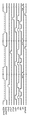
その後、画素群a、b、cを含む行の浮遊拡散層Cfd出力を保持容量211に保持するためにptn信号をLo→Hi→Loさせる。更に、画素信号を保持容量210に保持するためにpts信号をHiにするとともに、6行目の画素信号を浮遊拡散層Cfdに転送するためにptx_0信号をLo→Hi→Loにする。その後pts信号をHiにすることで、6行目の画素信号が保持容量210に保持される。その後Psel_024をLoにしてPres_024をHiにすることで画素群a、b、cを含む行の浮遊拡散層Cfdを再びリセットする。そして水平走査回路400によりph(n)信号が順次出力され6行目の信号が全画素分、順次読み出しアンプ216に読み出される。このときphadd信号はLoのままなので、出力信号は加算平均にはならない。ここまでが6行目の信号転送及び水平走査である。
Thereafter, in order to hold the floating diffusion layer Cfd output of the row including the pixel groups a, b, and c in the
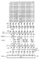
例えば、6、8、10行目の垂直同色画素加算後の画素では、4列目のR画素に焦点検出用画素が配置されているので、左右同色の2、6列目画素は読み出さず4列目画素のみを読み出す。そして、焦点検出用画素を含まないその他の画素列においては、ベイヤー画素配置時の色重心を考慮した水平方向の3画素の加算を行うようにしている。9、11、13行目の垂直同色3画素加算後の画素においても同様である。 For example, in the pixels after the vertical pixels of the same color the summing of 6,8,10 row, since the focus detection pixels in the R pixel in the fourth column are arranged, without reading the 2,6 row pixels of the left and right the same color Only the pixels in the fourth column are read out. In the other pixel columns not including the focus detection pixels, the horizontal three pixels are added in consideration of the color centroid when the Bayer pixels are arranged. The same applies to the pixels in the ninth, eleventh, and thirteenth rows after the addition of three pixels of the same color.
Claims (1)
Priority Applications (5)
| Application Number | Priority Date | Filing Date | Title |
|---|---|---|---|
| JP2010235877A JP5739640B2 (en) | 2010-10-20 | 2010-10-20 | Imaging device and imaging apparatus |
| KR1020137011980A KR101469400B1 (en) | 2010-10-20 | 2011-09-29 | Image sensor and image capturing apparatus |
| US13/877,598 US8988593B2 (en) | 2010-10-20 | 2011-09-29 | Image sensor and image capturing apparatus with focus detection pixels |
| CN201180050280.1A CN103168463B (en) | 2010-10-20 | 2011-09-29 | Imageing sensor and picture pick-up device |
| PCT/JP2011/073032 WO2012053363A1 (en) | 2010-10-20 | 2011-09-29 | Image sensor and image capturing apparatus |
Applications Claiming Priority (1)
| Application Number | Priority Date | Filing Date | Title |
|---|---|---|---|
| JP2010235877A JP5739640B2 (en) | 2010-10-20 | 2010-10-20 | Imaging device and imaging apparatus |
Publications (3)
| Publication Number | Publication Date |
|---|---|
| JP2012090118A JP2012090118A (en) | 2012-05-10 |
| JP2012090118A5 true JP2012090118A5 (en) | 2013-12-05 |
| JP5739640B2 JP5739640B2 (en) | 2015-06-24 |
Family
ID=45975081
Family Applications (1)
| Application Number | Title | Priority Date | Filing Date |
|---|---|---|---|
| JP2010235877A Active JP5739640B2 (en) | 2010-10-20 | 2010-10-20 | Imaging device and imaging apparatus |
Country Status (5)
| Country | Link |
|---|---|
| US (1) | US8988593B2 (en) |
| JP (1) | JP5739640B2 (en) |
| KR (1) | KR101469400B1 (en) |
| CN (1) | CN103168463B (en) |
| WO (1) | WO2012053363A1 (en) |
Families Citing this family (48)
| Publication number | Priority date | Publication date | Assignee | Title |
|---|---|---|---|---|
| JP5592944B2 (en) * | 2010-04-28 | 2014-09-17 | 富士フイルム株式会社 | Imaging device |
| JP5746496B2 (en) * | 2010-12-03 | 2015-07-08 | キヤノン株式会社 | Imaging device |
| JP5698555B2 (en) * | 2011-02-17 | 2015-04-08 | オリンパス株式会社 | Imaging device, imaging device |
| JP2013055500A (en) * | 2011-09-02 | 2013-03-21 | Sony Corp | Solid state imaging device and camera system |
| WO2014103852A1 (en) * | 2012-12-28 | 2014-07-03 | 富士フイルム株式会社 | Pixel correction method and image capture device |
| US9293500B2 (en) | 2013-03-01 | 2016-03-22 | Apple Inc. | Exposure control for image sensors |
| US9276031B2 (en) | 2013-03-04 | 2016-03-01 | Apple Inc. | Photodiode with different electric potential regions for image sensors |
| US9041837B2 (en) | 2013-03-05 | 2015-05-26 | Apple Inc. | Image sensor with reduced blooming |
| US9741754B2 (en) | 2013-03-06 | 2017-08-22 | Apple Inc. | Charge transfer circuit with storage nodes in image sensors |
| US9549099B2 (en) | 2013-03-12 | 2017-01-17 | Apple Inc. | Hybrid image sensor |
| US9319611B2 (en) | 2013-03-14 | 2016-04-19 | Apple Inc. | Image sensor with flexible pixel summing |
| US9826174B2 (en) * | 2013-03-26 | 2017-11-21 | Samsung Electronics Co., Ltd | Image processing apparatus and method |
| JP2015015596A (en) * | 2013-07-04 | 2015-01-22 | キヤノン株式会社 | Imaging device, and method of driving the same |
| JP6124717B2 (en) * | 2013-07-16 | 2017-05-10 | オリンパス株式会社 | Image sensor, focus detection device |
| JP6274788B2 (en) * | 2013-08-28 | 2018-02-07 | キヤノン株式会社 | Imaging apparatus, imaging system, and driving method of imaging apparatus |
| JP2015049283A (en) * | 2013-08-30 | 2015-03-16 | キヤノン株式会社 | Imaging device, imaging system, control method for imaging device, program, and storage medium |
| US9596423B1 (en) | 2013-11-21 | 2017-03-14 | Apple Inc. | Charge summing in an image sensor |
| US9596420B2 (en) | 2013-12-05 | 2017-03-14 | Apple Inc. | Image sensor having pixels with different integration periods |
| US9473706B2 (en) | 2013-12-09 | 2016-10-18 | Apple Inc. | Image sensor flicker detection |
| US10285626B1 (en) | 2014-02-14 | 2019-05-14 | Apple Inc. | Activity identification using an optical heart rate monitor |
| US9277144B2 (en) | 2014-03-12 | 2016-03-01 | Apple Inc. | System and method for estimating an ambient light condition using an image sensor and field-of-view compensation |
| US9232150B2 (en) | 2014-03-12 | 2016-01-05 | Apple Inc. | System and method for estimating an ambient light condition using an image sensor |
| US9584743B1 (en) | 2014-03-13 | 2017-02-28 | Apple Inc. | Image sensor with auto-focus and pixel cross-talk compensation |
| JP6305169B2 (en) * | 2014-04-07 | 2018-04-04 | キヤノン株式会社 | Solid-state imaging device, imaging apparatus, control method thereof, program, and storage medium |
| US9497397B1 (en) | 2014-04-08 | 2016-11-15 | Apple Inc. | Image sensor with auto-focus and color ratio cross-talk comparison |
| US9538106B2 (en) | 2014-04-25 | 2017-01-03 | Apple Inc. | Image sensor having a uniform digital power signature |
| JP6338436B2 (en) * | 2014-04-25 | 2018-06-06 | キヤノン株式会社 | Imaging apparatus and control method thereof |
| US9711553B2 (en) * | 2014-04-28 | 2017-07-18 | Samsung Electronics Co., Ltd. | Image sensor including a pixel having photoelectric conversion elements and image processing device having the image sensor |
| US9686485B2 (en) | 2014-05-30 | 2017-06-20 | Apple Inc. | Pixel binning in an image sensor |
| JP6530593B2 (en) * | 2014-08-11 | 2019-06-12 | キヤノン株式会社 | Imaging device, control method therefor, storage medium |
| KR102242472B1 (en) * | 2014-12-18 | 2021-04-20 | 엘지이노텍 주식회사 | Image sensor, image pick-up apparatus including the same and portable terminal including the apparatus |
| JP6595839B2 (en) * | 2015-08-05 | 2019-10-23 | キヤノン株式会社 | IMAGING ELEMENT, CONTROL METHOD THEREOF, AND IMAGING DEVICE |
| US9912883B1 (en) | 2016-05-10 | 2018-03-06 | Apple Inc. | Image sensor with calibrated column analog-to-digital converters |
| US10523860B2 (en) * | 2016-05-12 | 2019-12-31 | Canon Kabushiki Kaisha | Focus detection device, control method thereof, and image capture apparatus |
| TWI578785B (en) * | 2016-06-08 | 2017-04-11 | 群邁通訊股份有限公司 | Photographic device and photographic method |
| EP3712945A3 (en) | 2016-09-23 | 2020-12-02 | Apple Inc. | Stacked backside illuminated spad array |
| JP2018072390A (en) * | 2016-10-24 | 2018-05-10 | オリンパス株式会社 | Imaging device |
| CN110235024B (en) | 2017-01-25 | 2022-10-28 | 苹果公司 | SPAD detector with modulation sensitivity |
| US10656251B1 (en) | 2017-01-25 | 2020-05-19 | Apple Inc. | Signal acquisition in a SPAD detector |
| US10962628B1 (en) | 2017-01-26 | 2021-03-30 | Apple Inc. | Spatial temporal weighting in a SPAD detector |
| US10622538B2 (en) | 2017-07-18 | 2020-04-14 | Apple Inc. | Techniques for providing a haptic output and sensing a haptic input using a piezoelectric body |
| US10440301B2 (en) | 2017-09-08 | 2019-10-08 | Apple Inc. | Image capture device, pixel, and method providing improved phase detection auto-focus performance |
| CN107370959B (en) * | 2017-09-19 | 2019-11-29 | 德淮半导体有限公司 | Imaging sensor, imaging device and focusing method |
| US10848693B2 (en) | 2018-07-18 | 2020-11-24 | Apple Inc. | Image flare detection using asymmetric pixels |
| US11019294B2 (en) | 2018-07-18 | 2021-05-25 | Apple Inc. | Seamless readout mode transitions in image sensors |
| CN110855896A (en) * | 2019-12-13 | 2020-02-28 | 惠州Tcl移动通信有限公司 | Shooting method and device, storage medium and terminal equipment |
| US11563910B2 (en) | 2020-08-04 | 2023-01-24 | Apple Inc. | Image capture devices having phase detection auto-focus pixels |
| US11546532B1 (en) | 2021-03-16 | 2023-01-03 | Apple Inc. | Dynamic correlated double sampling for noise rejection in image sensors |
Family Cites Families (8)
| Publication number | Priority date | Publication date | Assignee | Title |
|---|---|---|---|---|
| JP4007713B2 (en) | 1999-04-06 | 2007-11-14 | オリンパス株式会社 | Imaging device |
| JP3968122B2 (en) | 2001-12-13 | 2007-08-29 | イーストマン コダック カンパニー | Imaging device |
| JP5040458B2 (en) | 2007-06-16 | 2012-10-03 | 株式会社ニコン | Solid-state imaging device and imaging apparatus using the same |
| JP5045350B2 (en) * | 2007-10-01 | 2012-10-10 | 株式会社ニコン | Imaging device and imaging apparatus |
| JP4403435B2 (en) * | 2007-11-16 | 2010-01-27 | ソニー株式会社 | Solid-state imaging device, drive control method, and imaging device |
| JP5127476B2 (en) * | 2008-01-28 | 2013-01-23 | キヤノン株式会社 | Imaging device |
| JP5241355B2 (en) * | 2008-07-10 | 2013-07-17 | キヤノン株式会社 | Imaging apparatus and control method thereof |
| JP5388544B2 (en) * | 2008-11-05 | 2014-01-15 | キヤノン株式会社 | Imaging apparatus and focus control method thereof |
-
2010
- 2010-10-20 JP JP2010235877A patent/JP5739640B2/en active Active
-
2011
- 2011-09-29 US US13/877,598 patent/US8988593B2/en active Active
- 2011-09-29 KR KR1020137011980A patent/KR101469400B1/en active IP Right Grant
- 2011-09-29 WO PCT/JP2011/073032 patent/WO2012053363A1/en active Application Filing
- 2011-09-29 CN CN201180050280.1A patent/CN103168463B/en active Active
Similar Documents
| Publication | Publication Date | Title |
|---|---|---|
| JP2012090118A5 (en) | ||
| JP5004775B2 (en) | Imaging apparatus and imaging system | |
| JP2015128215A5 (en) | ||
| JP2010147949A5 (en) | Imaging sensor, imaging system, and driving method of imaging sensor | |
| JP2013236362A5 (en) | ||
| JP2011511562A5 (en) | ||
| US8860858B2 (en) | Solid-state image sensor, driving method thereof, and camera | |
| JP2009206976A5 (en) | ||
| JP2011520351A5 (en) | ||
| JP2014023070A5 (en) | ||
| JP2013538518A5 (en) | ||
| JP2009117904A5 (en) | ||
| TW201230790A (en) | Solid-state image sensing device and camera system | |
| JP2006261789A5 (en) | ||
| JP2009194656A5 (en) | ||
| EP2309541A3 (en) | Solid-state image sensor and image sensing apparatus | |
| RU2015123466A (en) | IMAGE CAPTURE DEVICE AND METHOD FOR MANAGING THE IMAGE CAPTURE DEVICE | |
| JP2015026938A5 (en) | ||
| EP2339829A3 (en) | Sampling and readout of an image sensor | |
| JP2012513160A5 (en) | ||
| JP5075934B2 (en) | Solid-state imaging device and image recording device | |
| JP2016021052A5 (en) | ||
| JP2016042633A5 (en) | ||
| WO2014127376A3 (en) | High dynamic range cmos image sensor having anti-blooming properties and associated methods | |
| JP2007189537A5 (en) |