JP2012019503A - Antenna module - Google Patents
Antenna module Download PDFInfo
- Publication number
- JP2012019503A JP2012019503A JP2010287838A JP2010287838A JP2012019503A JP 2012019503 A JP2012019503 A JP 2012019503A JP 2010287838 A JP2010287838 A JP 2010287838A JP 2010287838 A JP2010287838 A JP 2010287838A JP 2012019503 A JP2012019503 A JP 2012019503A
- Authority
- JP
- Japan
- Prior art keywords
- resonator
- antenna
- surface wave
- wave radiation
- module according
- Prior art date
- Legal status (The legal status is an assumption and is not a legal conclusion. Google has not performed a legal analysis and makes no representation as to the accuracy of the status listed.)
- Pending
Links
Images


Classifications
-
- H—ELECTRICITY
- H01—ELECTRIC ELEMENTS
- H01Q—ANTENNAS, i.e. RADIO AERIALS
- H01Q9/00—Electrically-short antennas having dimensions not more than twice the operating wavelength and consisting of conductive active radiating elements
- H01Q9/04—Resonant antennas
- H01Q9/0407—Substantially flat resonant element parallel to ground plane, e.g. patch antenna
-
- H—ELECTRICITY
- H01—ELECTRIC ELEMENTS
- H01Q—ANTENNAS, i.e. RADIO AERIALS
- H01Q1/00—Details of, or arrangements associated with, antennas
- H01Q1/12—Supports; Mounting means
- H01Q1/22—Supports; Mounting means by structural association with other equipment or articles
- H01Q1/2283—Supports; Mounting means by structural association with other equipment or articles mounted in or on the surface of a semiconductor substrate as a chip-type antenna or integrated with other components into an IC package
-
- H—ELECTRICITY
- H01—ELECTRIC ELEMENTS
- H01Q—ANTENNAS, i.e. RADIO AERIALS
- H01Q1/00—Details of, or arrangements associated with, antennas
- H01Q1/36—Structural form of radiating elements, e.g. cone, spiral, umbrella; Particular materials used therewith
- H01Q1/38—Structural form of radiating elements, e.g. cone, spiral, umbrella; Particular materials used therewith formed by a conductive layer on an insulating support
-
- H—ELECTRICITY
- H01—ELECTRIC ELEMENTS
- H01Q—ANTENNAS, i.e. RADIO AERIALS
- H01Q19/00—Combinations of primary active antenna elements and units with secondary devices, e.g. with quasi-optical devices, for giving the antenna a desired directional characteristic
- H01Q19/005—Patch antenna using one or more coplanar parasitic elements
Landscapes
- Engineering & Computer Science (AREA)
- Microelectronics & Electronic Packaging (AREA)
- Waveguide Aerials (AREA)
- Details Of Aerials (AREA)
Abstract
Description
本発明はアンテナモジュールに関し、さらに詳細には、誘電体基板の表面に沿って流れる信号を放射して、ミリ波帯で広帯域特性を有しながら放射効率の高い高利得のアンテナモジュールに関する。 The present invention relates to an antenna module, and more particularly to a high gain antenna module having high radiation efficiency while radiating a signal flowing along the surface of a dielectric substrate and having broadband characteristics in the millimeter wave band.
ミリ波帯の周波数は波長が小さいためアンテナの小型化が容易であり、マイクロ波帯の周波数に比べて直進性に優れて広帯域特性を有するため、レーダーや広帯域通信サービスに用いられている。 Since the millimeter-wave band has a small wavelength, it is easy to reduce the size of the antenna. Since the millimeter-wave band is superior in straightness to the microwave band and has wideband characteristics, it is used for radar and broadband communication services.
このようなミリ波帯のシステムを構成するにあたり、製品の小型化及びコスト節減のためにSOP(System On Packaging)の形態を用いており、このようなSOPの方法としてLTCC(Low Temperature Cofired Ceramics)やLCP(Liquid Crystal Polymer)技術が考慮されている。このようなLTCCやLCP技術は基本的に多層基板を用いる技術であり、基板の内部にキャパシタ、インダクター、フィルターなどの手動部品を内蔵することができるため、モジュールの小型化と低価格化を果たすことができ、キャビティを自由に形成することができるため、モジュール構成の自由度が増加するという利点がある。 In configuring such a millimeter-wave band system, an SOP (System On Packaging) form is used to reduce the size and cost of the product, and as a method of such an SOP, LTCC (Low Temperature Conferred Ceramics) is used. And LCP (Liquid Crystal Polymer) technology is considered. Such LTCC and LCP technologies are basically technologies using a multilayer substrate, and manual components such as capacitors, inductors, filters, etc. can be built in the substrate, thereby reducing the size and cost of the module. In addition, since the cavity can be freely formed, there is an advantage that the degree of freedom of the module configuration is increased.
このようなSOPを用いたシステムの構成において、システムの性能を左右する要素の一つがパッチアンテナの具現である。しかし、ミリ波周波数帯、特に60GHz以上の超高周波帯で動作するパッチアンテナの場合、誘電体基板の表面に沿って流れる表面波の形態で信号の漏洩が発生するという問題があり、これは基板の厚さが増加するほど、基板の誘電率が高いほど大きくなる。このような信号の漏洩はアンテナの放射効率を落とし、結局アンテナ利得を減少させる。 In a system configuration using such an SOP, one of the factors that influence the performance of the system is the implementation of the patch antenna. However, in the case of a patch antenna that operates in a millimeter wave frequency band, particularly an ultrahigh frequency band of 60 GHz or more, there is a problem that signal leakage occurs in the form of a surface wave that flows along the surface of the dielectric substrate. As the thickness of the substrate increases, it increases as the dielectric constant of the substrate increases. Such signal leakage reduces the radiation efficiency of the antenna and eventually decreases the antenna gain.
また、60GHz帯の通信システムでは7GHz以上の広い帯域幅が求められているが、従来のパッチアンテナ構造ではこのような広い帯域幅を有するアンテナを具現することが不可能であるという問題がある。 In addition, a wide bandwidth of 7 GHz or more is required in a communication system of 60 GHz band, but there is a problem that it is impossible to implement an antenna having such a wide bandwidth with a conventional patch antenna structure.
従って、アンテナ部分のみをLTCCのようなセラミックス基板に比べて相対的に誘電率が低い有機基板で製作して用いているが、この場合、LTCC単一基板上にアンテナを含む全体SOPモジュールの形態で製作するよりモジュールの大きさと製作コストが増加するという問題がある。 Therefore, only the antenna portion is manufactured and used on an organic substrate having a relatively low dielectric constant compared to a ceramic substrate such as LTCC. In this case, the configuration of the entire SOP module including the antenna on the LTCC single substrate is used. There is a problem that the size of the module and the manufacturing cost increase compared to the case of manufacturing by the above method.
従って、本発明は上述のような従来技術の問題点を解決するためのもので、LTCCのような誘電率が高い多層基板上に表面波の進行を抑制して表面波形態の信号を再放射することにより、アンテナの効率と利得を高め、アンテナの帯域を広げることができるアンテナ構造が 具現されたアンテナモジュールを提供することをその目的とする。 Accordingly, the present invention is to solve the above-mentioned problems of the prior art, and re-radiates a surface wave form signal by suppressing the progress of the surface wave on a multilayer substrate having a high dielectric constant such as LTCC. Accordingly, an object of the present invention is to provide an antenna module in which an antenna structure that can increase the efficiency and gain of the antenna and widen the band of the antenna is realized.
上述の技術的課題を果たすための本発明の一実施形態によるアンテナモジュールは、誘電体基板の表面に形成されるパッチアンテナ共振器と、前記パッチアンテナ共振器と離隔されて配置され、前記パッチアンテナ共振器から前記誘電体基板の表面に沿って流れる信号を放射させるように前記パッチアンテナ共振器の周辺を取り囲む表面波放射共振器を含むことができる。 An antenna module according to an embodiment of the present invention for achieving the above technical problem is provided with a patch antenna resonator formed on a surface of a dielectric substrate, and spaced apart from the patch antenna resonator. A surface wave radiation resonator may be included that surrounds the periphery of the patch antenna resonator so as to radiate a signal flowing along the surface of the dielectric substrate from the resonator.
また、本発明の一実施形態によるアンテナモジュールにおいて、前記表面波放射共振器は金属帯の形状を有することができる。 In the antenna module according to the embodiment of the present invention, the surface wave radiation resonator may have a metal band shape.
また、本発明の一実施形態によるアンテナモジュールにおいて、前記パッチアンテナ共振器は円形パッチであり、前記表面波放射共振器は円形リングの形状で前記パッチアンテナの周辺を取り囲むように形成されることができる。 In the antenna module according to the embodiment of the present invention, the patch antenna resonator may be a circular patch, and the surface wave radiation resonator may be formed in a circular ring shape so as to surround the periphery of the patch antenna. it can.
また、本発明の一実施形態によるアンテナモジュールにおいて、前記パッチアンテナ共振器は四角形パッチであり、前記表面波放射共振器は四角リング形状で前記パッチアンテナの周辺を取り囲むように形成されることができる。 In the antenna module according to an embodiment of the present invention, the patch antenna resonator may be a rectangular patch, and the surface wave radiation resonator may be formed in a square ring shape so as to surround the periphery of the patch antenna. .
また、本発明の一実施形態によるアンテナモジュールにおいて、前記パッチアンテナ共振器は一側にフィードラインを備えて、前記表面波放射共振器は前記フィードラインが通過するようにスロットを備えることができる。 In the antenna module according to an embodiment of the present invention, the patch antenna resonator may include a feed line on one side, and the surface wave radiating resonator may include a slot through which the feed line passes.
また、本発明の一実施形態によるアンテナモジュールは、前記誘電体基板の厚さ方向に前記表面波放射共振器に対応する位置に形成される第2の表面波放射共振器と、前記表面波放射共振器と前記第2の表面波放射共振器を電気的に連結するビアをさらに含むことができる。 An antenna module according to an embodiment of the present invention includes a second surface wave radiation resonator formed at a position corresponding to the surface wave radiation resonator in a thickness direction of the dielectric substrate, and the surface wave radiation. A via may be further included to electrically connect the resonator and the second surface wave radiation resonator.
また、本発明の一実施形態によるアンテナモジュールにおいて、前記表面波放射共振器は前記パッチアンテナ共振器の周波数帯で共振することができるサイズに設計されることができる。 In the antenna module according to the embodiment of the present invention, the surface wave radiation resonator may be designed to have a size capable of resonating in the frequency band of the patch antenna resonator.
また、本発明の一実施形態によるアンテナモジュールにおいて、前記表面波放射共振器は前記パッチアンテナ共振器の周波数帯と近い周波数帯で共振することができるサイズに設計されることができる。 In the antenna module according to the embodiment of the present invention, the surface wave radiation resonator may be designed to have a size capable of resonating in a frequency band close to the frequency band of the patch antenna resonator.
また、本発明の一実施形態によるアンテナモジュールにおいて、前記表面波放射共振器の共振周波数は前記表面波放射共振器の幅、厚さ、及び前記パッチアンテナ共振器との間隔によって決まることができる。 In the antenna module according to the embodiment of the present invention, the resonance frequency of the surface wave radiation resonator may be determined by the width and thickness of the surface wave radiation resonator and the distance from the patch antenna resonator.
また、本発明の一実施形態によるアンテナモジュールは、前記パッチアンテナ共振器と前記表面波放射共振器の共振ピークをカップリングしてアンテナの帯域幅を拡張させることができる。 The antenna module according to an embodiment of the present invention can extend the bandwidth of the antenna by coupling resonance peaks of the patch antenna resonator and the surface wave radiation resonator.
また、本発明の一実施形態によるアンテナモジュールにおいて、前記誘電体基板はグランドパターンが形成された回路基板に連結されることができる。 In the antenna module according to the embodiment of the present invention, the dielectric substrate may be connected to a circuit substrate on which a ground pattern is formed.
また、本発明の一実施形態によるアンテナモジュールにおいて、前記パッチアンテナ共振器と前記表面波放射共振器はミリ波帯の周波数で動作することができる。 In the antenna module according to the embodiment of the present invention, the patch antenna resonator and the surface wave radiation resonator can operate at a frequency in a millimeter wave band.
また、本発明の一実施形態によるアンテナモジュールにおいて、前記誘電体基板はLTCCまたはLCPからなることができる。 In the antenna module according to an embodiment of the present invention, the dielectric substrate may be made of LTCC or LCP.
本発明によるアンテナモジュールによると、パッチアンテナ共振器の周りに表面波放射共振器を配置することにより、誘電体基板から表面波形態で信号が漏洩されることを防止し、またパッチアンテナ共振器から表面波放射共振器に流れる信号を再放射することにより、アンテナの放射効率と利得を高めることができる。 According to the antenna module of the present invention, by disposing a surface wave radiation resonator around the patch antenna resonator, it is possible to prevent signals from leaking in the form of surface waves from the dielectric substrate, and from the patch antenna resonator. By re-radiating the signal flowing in the surface wave radiation resonator, the radiation efficiency and gain of the antenna can be increased.
また、本発明によるアンテナモジュールによると、パッチアンテナ共振器と表面波放射共振器のカップリングを調節して、アンテナの帯域幅を拡張することができる。 According to the antenna module of the present invention, the antenna bandwidth can be expanded by adjusting the coupling between the patch antenna resonator and the surface wave radiation resonator.
以下、図面を参照して本発明の具体的な実施形態を詳細に説明する。但し、本発明の思想は提示される実施形態に制限されず、本発明の思想を理解する当業者は同一の思想の範囲内にて他の構成要素を追加、変更、削除等によって、退歩的な他の発明や本発明の思想の範囲内に含まれる他の実施形態を容易に提案することができるが、これもまた本発明の思想の範囲内に含まれるとするべきであろう。 Hereinafter, specific embodiments of the present invention will be described in detail with reference to the drawings. However, the idea of the present invention is not limited to the embodiments shown, and those skilled in the art who understand the idea of the present invention can perform a regressive process by adding, changing, or deleting other components within the scope of the same idea. Although other embodiments within the scope of the idea of the present invention and other embodiments can be easily proposed, they should also be included within the scope of the idea of the present invention.
また、各実施形態の図面に示される同一の思想の範囲内の機能が同一の構成要素は、同一または類似の参照符号を用いて説明する。 In addition, constituent elements having the same functions within the scope of the same idea shown in the drawings of the embodiments will be described using the same or similar reference numerals.
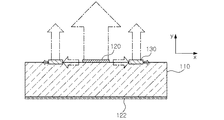
図1は本発明の第1実施形態によるアンテナモジュールの平面図であり、図2は本発明の第1実施形態によるアンテナモジュールで信号の放射を示す厚さ方向の断面図であり、図3a及び図3bは本発明の第1実施形態によるアンテナモジュールの反射特性(S11)及び放射特性(アンテナ利得)を示すグラフである。 FIG. 1 is a plan view of an antenna module according to a first embodiment of the present invention, and FIG. 2 is a cross-sectional view in the thickness direction illustrating signal radiation in the antenna module according to the first embodiment of the present invention. FIG. 3B is a graph showing reflection characteristics (S11) and radiation characteristics (antenna gain) of the antenna module according to the first embodiment of the present invention.
図1から図3を参照すると、本発明の第1実施形態によるアンテナモジュールは、誘電体基板110上に形成されるパッチアンテナ共振器120と表面波放射共振器130を含む。
1 to 3, the antenna module according to the first embodiment of the present invention includes a
上記誘電体基板110は、シリコン(Si)のような半導体基板、高周波用低温同時焼成セラミックス(Low Temperature Co−fired Ceramics:LTCC)のようなセラミックス基板、液晶高分子(Liquid Crystal Polymer:LCP)のような有機基板などで具現されることができる。
The
本実施形態で、誘電体基板110は誘電率が9.2、誘電損失が0.002であり、一層の厚さが0.06mmであるLTCC基板を6層積層し、総基板の厚さが0.36mmである基板に設計することができる。
In this embodiment, the
パッチアンテナ共振器120は誘電体基板110の表面に円形パッチの形態で形成されて、円形パッチの一側にフィードライン121が連結される。誘電体基板110の裏面にはグランド122が形成される。
The
表面波放射共振器130は、誘電体基板110上にパッチアンテナ共振器120から漏洩される信号を放射するようにパッチアンテナ共振器120の周辺に一定間隔だけ離れて形成される。
The surface
表面波放射共振器130は金属帯の形状を有することができ、パッチアンテナ共振器120の一側に形成されたフィードライン121が通過することができるようにスロット135を備える。
The surface
表面波放射共振器130はパッチアンテナ共振器120の周辺を取り囲むように形成されるため、パッチアンテナ共振器120の周りと対応する形状を有する。即ち、本実施形態でパッチアンテナ共振器120が円形パッチからなるため、表面波放射共振器130はパッチアンテナ共振器120と同一の中心を有する円形リングの形状を有する。
Since the surface
表面波放射共振器130はパッチアンテナ共振器120から誘電体基板110の表面に沿って流れる信号を放射するようにサイズが決められることができる。例えば、表面波放射共振器130はパッチアンテナ共振器120の周波数帯と近い周波数帯で共振することができるサイズに設計されたり、パッチアンテナ共振器120の周波数帯で共振することができるサイズに設計されることができる。
The surface
この時、表面波放射共振器130の幅、厚さ、パッチアンテナ共振器120との間隔、スロット135の幅を調整することにより、表面波放射共振器130のピークとパッチアンテナ共振器120のピークを適切にカップリングすると、アンテナの帯域幅を拡張させることが可能である。表面波放射共振器130の厚さは、パッチアンテナ共振器120の表面波信号が遮断及び放射するように、パッチアンテナ共振器120の厚さと実質的に同一またはそれより大きいことが好ましい。
At this time, the peak of the surface
本実施形態では、パッチアンテナ共振器120の直径を0.67mm、表面波放射共振器130の幅を0.59mm、厚さを10μm、外径を1.45mm、スロット135の幅を0.3mm、フィードライン121の幅を0.08mmに設計し、この時のアンテナ特性としてHFSS(High Frequency Simulation Software)を用いた電磁場模写実験によって測定して示したのが図3a及び図3bである。
In this embodiment, the diameter of the
図3aに図示されたように、本実施形態によるアンテナモジュールは周波数帯が57.5〜63.7GHzで6.2GHzの帯域幅を有し、二重共振器による二つのポール(pole)が存在することが分かる。即ち、パッチアンテナ共振器120とその周辺を取り囲む表面波放射共振器130の共振ピークが存在し、この二つの共振ピークのカップリングの程度を調節することによりアンテナモジュールの帯域幅を調節することができる。
As shown in FIG. 3a, the antenna module according to the present embodiment has a frequency band of 57.5 to 63.7 GHz and a bandwidth of 6.2 GHz, and there are two poles due to a double resonator. I understand that That is, there is a resonance peak of the surface
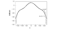
また、図3bに図示されたように、本実施形態によるアンテナモジュールの利得は9.6dBiであることが分かり、フィードライン121に垂直の方向(Φ=90゜)と水平の方向(Φ=0゜)での利得がほぼ類似であることが分かる。この時、アンテナモジュールの放射効率は60.8%である。 Also, as shown in FIG. 3b, it can be seen that the gain of the antenna module according to the present embodiment is 9.6 dBi, and the direction perpendicular to the feed line 121 (Φ = 90 °) and the horizontal direction (Φ = 0). It can be seen that the gain at (°) is almost similar. At this time, the radiation efficiency of the antenna module is 60.8%.
図8a及び図8bは比較例によるアンテナモジュールの反射特性(S11)及び放射特性(アンテナ利得)を示すグラフである。比較例によるアンテナモジュールは一般的な誘電体基板上に具現されたパッチアンテナであり、誘電率が9.2、誘電損失が0.002であり、一層の厚さが0.06mmであるLTCC基板を6層積層し、総基板の厚さが0.36mmである誘電体基板を用いている。 8a and 8b are graphs showing the reflection characteristic (S11) and radiation characteristic (antenna gain) of the antenna module according to the comparative example. The antenna module according to the comparative example is a patch antenna implemented on a general dielectric substrate, and has a dielectric constant of 9.2, a dielectric loss of 0.002, and a single layer thickness of 0.06 mm. Is used, and a dielectric substrate having a total substrate thickness of 0.36 mm is used.
図8aに図示されたように、比較例によるアンテナモジュールの周波数帯は59.3〜62GHzで2.7GHzの帯域幅を有し、図8bに図示されたように、アンテナ利得は2.5dBiであり、アンテナ放射効率は25%である。 As illustrated in FIG. 8a, the frequency band of the antenna module according to the comparative example has a bandwidth of 2.7 GHz at 59.3 to 62 GHz, and the antenna gain is 2.5 dBi as illustrated in FIG. 8b. The antenna radiation efficiency is 25%.
従って、本発明の第1実施形態によるアンテナモジュールは、比較例によるアンテナモジュールに比べて、帯域幅が約3倍程度広く、アンテナ利得が約4倍程度高くて、アンテナ放射効率は約2.5倍程度より大きく表れることが分かる。 Therefore, the antenna module according to the first embodiment of the present invention has a bandwidth about 3 times wider, an antenna gain about 4 times higher, and an antenna radiation efficiency of about 2.5 compared to the antenna module according to the comparative example. It turns out that it appears larger than about twice.
これは図2に示したように、本実施形態によるアンテナモジュールにおいて、パッチアンテナ共振器120から誘電体基板110の表面に沿って漏洩される信号(x軸方向の矢印)が表面波放射共振器130で再び放射(y軸方向の矢印)されるためである。
As shown in FIG. 2, in the antenna module according to the present embodiment, a signal (arrow in the x-axis direction) leaked from the
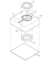
図4は本発明の第2実施形態によるアンテナモジュールの分解斜視図であり、図5は本発明の第2実施形態によるアンテナモジュールで信号の放射を示す厚さ方向の断面図である。 FIG. 4 is an exploded perspective view of an antenna module according to the second embodiment of the present invention, and FIG. 5 is a cross-sectional view in the thickness direction showing signal radiation in the antenna module according to the second embodiment of the present invention.
図4及び図5に図示された本発明の第2実施形態によるアンテナモジュールは、誘電体基板の表面だけでなく内部にも表面波放射共振器が形成されたものであり、他の構成は図1に図示された本発明の第1実施形態によるアンテナモジュールと同一であるため、この構成に対する詳細な説明は省略し、以下では差異点を中心に説明する。 The antenna module according to the second embodiment of the present invention shown in FIGS. 4 and 5 has a surface wave radiating resonator formed not only on the surface of the dielectric substrate but also on the inside thereof. 1 is the same as the antenna module according to the first embodiment of the present invention illustrated in FIG. 1, and thus detailed description of this configuration is omitted, and the following description focuses on the differences.
図4及び図5を参照すると、本発明の第2実施形態によるアンテナモジュールは、誘電体基板210上に形成されたパッチアンテナ共振器220を含み、上記パッチアンテナ共振器220の一側にはフィードライン221を備え、誘電体基板210の裏面にはグランド222を含む。
4 and 5, the antenna module according to the second embodiment of the present invention includes a
一方、誘電体基板210上には、パッチアンテナ共振器220の周辺を取り囲むように円形リング形状の第1の表面波放射共振器231がパッチアンテナ共振器220から所定間隔だけ離れて形成され、誘電体基板210の厚さ方向の内部には、上記第1の表面波放射共振器231と対応する位置に円形リング形状の第2の表面波放射共振器232が形成されている。
On the other hand, a circular ring-shaped first surface
この時、上記第1の表面波放射共振器231と第2の表面波放射共振器232は、誘電体基板210の厚さ方向に形成されるビア233によって連結される。ビア233は第1及び第2の表面波放射共振器の周りに沿って配置されることができる。
At this time, the first surface
第1の表面波放射共振器231と第2の表面波放射共振器232は同一のサイズに設計されることができ、求める周波数帯や帯域幅によって異なるサイズに設計されることもできる。即ち、本実施形態のように第2の表面波放射共振器232の厚さをより大きく設計することもできる。
The first surface
本実施形態によるアンテナモジュールの特性は次の通りである。 The characteristics of the antenna module according to the present embodiment are as follows.

上記表1に示されたように、第1の表面波放射共振器231の厚さが第2の表面波放射共振器232の厚さより半分程度小さくても、ほぼ同一のアンテナ特性を表すことが分かる。
As shown in Table 1 above, even if the thickness of the first surface
第2の表面波放射共振器232は誘電体基板210の内部層に形成されることもでき、図5のように誘電体基板210の裏面にキャビティを形成して内蔵することもできる。
The second surface
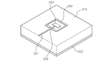
図6は本発明の第3実施形態によるアンテナモジュールの斜視図であり、図7a及び図7bは本発明の第3実施形態によるアンテナモジュールの反射特性(S11)及び放射特性(アンテナ利得)を示すグラフである。 FIG. 6 is a perspective view of an antenna module according to a third embodiment of the present invention, and FIGS. 7a and 7b show reflection characteristics (S11) and radiation characteristics (antenna gain) of the antenna module according to the third embodiment of the present invention. It is a graph.
図6及び図7に図示された本発明の第3実施形態によるアンテナモジュールは、パッチアンテナ共振器が四角形パッチからなり、表面波放射共振器が四角リングの形状に形成されるものであり、他の構成は図1に図示された本発明の第1実施形態によるアンテナモジュールと同一であるため、この構成に対する詳細な説明は省略し、以下では差異点を中心に説明する。 In the antenna module according to the third embodiment of the present invention shown in FIGS. 6 and 7, the patch antenna resonator is formed of a rectangular patch, and the surface wave radiation resonator is formed in the shape of a square ring. Since this configuration is the same as that of the antenna module according to the first embodiment of the present invention shown in FIG. 1, a detailed description thereof will be omitted, and the following description will focus on the differences.
図6を参照すると、本発明の第3実施形態によるアンテナモジュールは、誘電体基板310上にパッチアンテナ共振器320と表面波放射共振器330を含む。
Referring to FIG. 6, the antenna module according to the third embodiment of the present invention includes a
パッチアンテナ共振器320は四角形パッチからなり、一側にフィードライン321を備え、誘電体基板310の裏面に形成されたグランド322と接地される。
The
表面波放射共振器330は、誘電体基板310上にパッチアンテナ共振器320から漏洩される信号を放射するようにパッチアンテナ共振器320の周辺に一定間隔だけ離れて形成される。
The surface
表面波放射共振器330は金属帯の形状を有することができ、パッチアンテナ共振器320の一側に形成されたフィードライン321が通過することができるようにスロット335を備える。
The surface
表面波放射共振器330はパッチアンテナ共振器320の周辺を取り囲むように形成されるため、パッチアンテナ共振器320の周りと対応する形状を有する。即ち、本実施形態でパッチアンテナ共振器320が四角形パッチからなるため、表面波放射共振器330は四角形リングの形状を有する。
Since the surface
本実施形態によるアンテナモジュールの特性をHFSS(High Frequency Simulation Software)を用いた電磁場模写実験によって測定して示したのが図7a及び図7bである。 FIG. 7A and FIG. 7B show the characteristics of the antenna module according to the present embodiment as measured by an electromagnetic field replication experiment using HFSS (High Frequency Simulation Software).
図7aに図示されたように、本実施形態によるアンテナモジュールは周波数帯が55.8〜66GHzで10.2GHzの帯域幅を有し、図7bに図示されたように、アンテナ利得が7.1dBiであることが分かり、フィードライン321に垂直の方向(Φ=90゜)と水平の方向(Φ=0゜)での利得がほぼ類似することが分かる。 As shown in FIG. 7a, the antenna module according to the present embodiment has a frequency band of 55.8 to 66 GHz and a bandwidth of 10.2 GHz. As shown in FIG. 7b, the antenna gain is 7.1 dBi. It can be seen that the gains in the direction perpendicular to the feed line 321 (Φ = 90 °) and in the horizontal direction (Φ = 0 °) are almost similar.
従って、本実施形態によるアンテナモジュールは、図8a及び図8bに図示された比較例によるアンテナモジュールの特性に比べて大きく向上された特性を表すことが分かる。 Accordingly, it can be seen that the antenna module according to the present embodiment exhibits characteristics that are greatly improved as compared with the characteristics of the antenna module according to the comparative example illustrated in FIGS. 8a and 8b.
以上、本発明の好ましい実施形態を詳細に説明したが、これは例示的なものに過ぎず、当該分野にて通常の知識を有する者であれば、これから多様な変形及び均等な他の実施形態が可能であることを理解するであろう。例えば、本発明で誘電体基板の誘電率、誘電損失のような特性、厚さや積層数は求められる設計条件によって多様に変更されることができる。また、パッチアンテナ共振器または表面派放射共振器の寸法や形態、表面派放射共振器の配置形態なども求められる設計条件及び仕様によって多様に変更されることができる。例えば、本発明の第2実施形態で表面派放射共振器を二つの層で形成することを例として説明したが、これは例示的なものであり、3層以上で形成することも可能である。従って、本発明の真正な技術的保護範囲は添付の特許請求範囲によって決まるべきであろう。 Although the preferred embodiment of the present invention has been described in detail above, this is merely an example, and various modifications and other equivalent embodiments will be made by those having ordinary knowledge in the art. You will understand that is possible. For example, in the present invention, characteristics such as dielectric constant, dielectric loss, thickness, and number of layers of the dielectric substrate can be variously changed according to required design conditions. In addition, the size and form of the patch antenna resonator or the surface radiating resonator, the arrangement form of the surface radiating resonator, and the like can be variously changed according to the required design conditions and specifications. For example, in the second embodiment of the present invention, the surface radiating resonator is formed with two layers as an example. However, this is only an example, and it is possible to form the surface radiating resonator with three or more layers. . Accordingly, the true technical protection scope of the present invention should be determined by the appended claims.
110、210、310 誘電体基板
120、220、320 パッチアンテナ共振器
121、221、321 フィードライン
122、222、322 グランド
130、231、232、330 表面波放射共振器
135、235、335 スロット
110, 210, 310
Claims (13)
前記パッチアンテナ共振器と離隔されて配置され、前記パッチアンテナ共振器から前記誘電体基板の表面に沿って流れる信号を放射させるように前記パッチアンテナ共振器の周辺を取り囲む表面波放射共振器と
を含むアンテナモジュール。 A patch antenna resonator formed on the surface of the dielectric substrate;
A surface wave radiating resonator that is spaced apart from the patch antenna resonator and surrounds the periphery of the patch antenna resonator so as to radiate a signal flowing from the patch antenna resonator along the surface of the dielectric substrate. Including antenna module.
前記表面波放射共振器は円形リングの形状で前記パッチアンテナ共振器の周辺を取り囲むように形成されることを特徴とする請求項1に記載のアンテナモジュール。 The patch antenna resonator is a circular patch;
The antenna module according to claim 1, wherein the surface wave radiation resonator is formed in a circular ring shape so as to surround a periphery of the patch antenna resonator.
前記表面波放射共振器は四角リング形状で前記パッチアンテナ共振器の周辺を取り囲むように形成されることを特徴とする請求項1に記載のアンテナモジュール。 The patch antenna resonator is a rectangular patch;
2. The antenna module according to claim 1, wherein the surface wave radiation resonator is formed in a square ring shape so as to surround a periphery of the patch antenna resonator.
前記表面波放射共振器は前記フィードラインが通過するようにスロットを備えることを特徴とする請求項1に記載のアンテナモジュール。 The patch antenna resonator includes a feed line on one side,
The antenna module according to claim 1, wherein the surface wave radiation resonator includes a slot through which the feed line passes.
前記表面波放射共振器と前記第2の表面波放射共振器を電気的に連結するビアと
をさらに含むことを特徴とする請求項1に記載のアンテナモジュール。 A second surface wave radiation resonator formed at a position corresponding to the surface wave radiation resonator in the thickness direction of the dielectric substrate;
The antenna module according to claim 1, further comprising a via electrically connecting the surface wave radiation resonator and the second surface wave radiation resonator.
Applications Claiming Priority (2)
| Application Number | Priority Date | Filing Date | Title |
|---|---|---|---|
| KR1020100064914A KR20120004188A (en) | 2010-07-06 | 2010-07-06 | Antenna module |
| KR10-2010-0064914 | 2010-07-06 |
Publications (1)
| Publication Number | Publication Date |
|---|---|
| JP2012019503A true JP2012019503A (en) | 2012-01-26 |
Family
ID=45372695
Family Applications (1)
| Application Number | Title | Priority Date | Filing Date |
|---|---|---|---|
| JP2010287838A Pending JP2012019503A (en) | 2010-07-06 | 2010-12-24 | Antenna module |
Country Status (4)
| Country | Link |
|---|---|
| US (1) | US20120007781A1 (en) |
| JP (1) | JP2012019503A (en) |
| KR (1) | KR20120004188A (en) |
| DE (1) | DE102010056573A1 (en) |
Cited By (1)
| Publication number | Priority date | Publication date | Assignee | Title |
|---|---|---|---|---|
| JP2020036197A (en) * | 2018-08-30 | 2020-03-05 | キヤノン株式会社 | Element and method for manufacturing the same |
Families Citing this family (18)
| Publication number | Priority date | Publication date | Assignee | Title |
|---|---|---|---|---|
| KR101313018B1 (en) * | 2012-02-08 | 2013-10-01 | 홍익대학교 산학협력단 | Dual-band Circular Polarized Patch Antenna using metamaterial |
| CN103606744B (en) * | 2013-11-07 | 2015-06-03 | 中国计量学院 | Dual concentric opening circular patch antenna |
| KR102063826B1 (en) * | 2014-01-23 | 2020-01-08 | 엘지이노텍 주식회사 | Antenna apparatus for radar system |
| US9748654B2 (en) | 2014-12-16 | 2017-08-29 | Laird Technologies, Inc. | Antenna systems with proximity coupled annular rectangular patches |
| CN104681972B (en) * | 2015-02-15 | 2017-06-23 | 重庆大学 | There is the groove loading ultra-wideband monopole antenna of stabilising direction figure and good Out-of-band rejection ability simultaneously |
| JP6525249B2 (en) * | 2015-03-20 | 2019-06-05 | カシオ計算機株式会社 | Antenna device and electronic device |
| KR20180047392A (en) * | 2016-10-31 | 2018-05-10 | 삼성전자주식회사 | Antenna apparatus |
| WO2018182507A1 (en) * | 2017-03-31 | 2018-10-04 | Agency For Science, Technology And Research | Compact wideband high gain circularly polarized antenna |
| KR102486593B1 (en) * | 2017-12-19 | 2023-01-10 | 삼성전자 주식회사 | Antenna module supproting radiation of vertical polarization and electric device including the antenna module |
| US10969282B2 (en) | 2018-07-05 | 2021-04-06 | Florida State University Research Foundation, Inc. | Wireless temperature sensors and methods |
| US20220011173A1 (en) * | 2018-07-05 | 2022-01-13 | Florida State University Research Foundation, Inc. | Wireless Temperature Sensors and Methods |
| TWI696315B (en) * | 2019-01-30 | 2020-06-11 | 友達光電股份有限公司 | Antenna device and antenna system |
| CN112467356B (en) * | 2019-09-09 | 2024-01-02 | 北京小米移动软件有限公司 | Antenna assembly and terminal |
| CN112542686B (en) * | 2019-09-23 | 2024-03-26 | 北京小米移动软件有限公司 | Antenna assembly and terminal equipment |
| KR102454942B1 (en) * | 2021-03-17 | 2022-10-13 | 홍익대학교 산학협력단 | Array antenna using fractal antenna |
| TWI764682B (en) * | 2021-04-22 | 2022-05-11 | 和碩聯合科技股份有限公司 | Antenna module |
| CN115882223A (en) * | 2021-09-30 | 2023-03-31 | 华为技术有限公司 | Dual-band dual-circularly polarized antenna and antenna system |
| CN114094301B (en) * | 2021-10-28 | 2023-03-24 | 西安理工大学 | Preparation method of magnetic-dielectric composite material dielectric resonator and miniaturized antenna |
Citations (3)
| Publication number | Priority date | Publication date | Assignee | Title |
|---|---|---|---|---|
| JP2001094339A (en) * | 1999-09-27 | 2001-04-06 | Mitsubishi Electric Corp | Composite antenna |
| JP2002198724A (en) * | 2000-12-25 | 2002-07-12 | Matsushita Electric Works Ltd | Microstrip antenna |
| JP2004007559A (en) * | 2002-04-25 | 2004-01-08 | Matsushita Electric Ind Co Ltd | Multiple-resonance antenna, antenna module, and radio device using the multiple-resonance antenna |
Family Cites Families (3)
| Publication number | Priority date | Publication date | Assignee | Title |
|---|---|---|---|---|
| US4063246A (en) * | 1976-06-01 | 1977-12-13 | Transco Products, Inc. | Coplanar stripline antenna |
| KR100988909B1 (en) * | 2008-09-23 | 2010-10-20 | 한국전자통신연구원 | Microstrip patch antenna with high gain and wide band characteristics |
| KR101040347B1 (en) | 2008-12-05 | 2011-06-10 | 현대자동차주식회사 | System for calculation efficiency conversion of selective catalytic reduction in diesel vehicle and method thereof |
-
2010
- 2010-07-06 KR KR1020100064914A patent/KR20120004188A/en not_active Application Discontinuation
- 2010-12-24 JP JP2010287838A patent/JP2012019503A/en active Pending
- 2010-12-30 DE DE102010056573A patent/DE102010056573A1/en not_active Ceased
-
2011
- 2011-01-04 US US12/984,081 patent/US20120007781A1/en not_active Abandoned
Patent Citations (3)
| Publication number | Priority date | Publication date | Assignee | Title |
|---|---|---|---|---|
| JP2001094339A (en) * | 1999-09-27 | 2001-04-06 | Mitsubishi Electric Corp | Composite antenna |
| JP2002198724A (en) * | 2000-12-25 | 2002-07-12 | Matsushita Electric Works Ltd | Microstrip antenna |
| JP2004007559A (en) * | 2002-04-25 | 2004-01-08 | Matsushita Electric Ind Co Ltd | Multiple-resonance antenna, antenna module, and radio device using the multiple-resonance antenna |
Cited By (2)
| Publication number | Priority date | Publication date | Assignee | Title |
|---|---|---|---|---|
| JP2020036197A (en) * | 2018-08-30 | 2020-03-05 | キヤノン株式会社 | Element and method for manufacturing the same |
| JP7118813B2 (en) | 2018-08-30 | 2022-08-16 | キヤノン株式会社 | Device, method for manufacturing device |
Also Published As
| Publication number | Publication date |
|---|---|
| US20120007781A1 (en) | 2012-01-12 |
| KR20120004188A (en) | 2012-01-12 |
| DE102010056573A1 (en) | 2012-01-12 |
Similar Documents
| Publication | Publication Date | Title |
|---|---|---|
| JP2012019503A (en) | Antenna module | |
| Saeidi et al. | Ultra‐wideband antennas for wireless communication applications | |
| US8319689B2 (en) | Patch antenna with wide bandwidth at millimeter wave band | |
| KR100917847B1 (en) | Omni-directional planar antenna | |
| TWI327789B (en) | Slit loaded tapered slot patch antenna | |
| KR101757719B1 (en) | Antenna | |
| JP5983769B2 (en) | Multiband antenna | |
| WO2016121375A1 (en) | Frequency selective surface, wireless communication device and radar device | |
| KR102211392B1 (en) | Patch antenna | |
| US20080204327A1 (en) | Compact dual-band resonator using anisotropic metamaterial | |
| KR20150087595A (en) | Dielectric resonator antenna | |
| KR20120088484A (en) | Antenna structure using multilayered substrate | |
| EP2631991B1 (en) | Microstrip antenna | |
| TW201328026A (en) | Circular polarization antenna | |
| US9853359B2 (en) | Antenna integrated in a package substrate | |
| JP2018536358A (en) | Dual-polarized planar ultra-wideband antenna | |
| Hu et al. | 60 GHz Fabry–Pérot cavity filtering antenna driven by an SIW-fed filtering source | |
| US10230161B2 (en) | Low-band reflector for dual band directional antenna | |
| TWI566474B (en) | Multi-band antenna | |
| Das et al. | Design of UWB Planar Monopole Antennas with Etched Spiral Slot on the Patch for Multiple Band‐Notched Characteristics | |
| TWI459634B (en) | Annular slot ring antenna | |
| KR101611794B1 (en) | Dual-band metamaterial circulary polarized antenna for gps applications | |
| WO2021060974A1 (en) | Antenna device which is suitable for wireless communications according to a 5g network standard, rf transceiver containing an antenna device, and method for use in wireless communications according to a 5g network standard | |
| Lee et al. | V-band integrated filter and antenna for LTCC front-end modules | |
| Rajesh et al. | A study of CSRR loaded microstrip antenna for multiband applications |
Legal Events
| Date | Code | Title | Description |
|---|---|---|---|
| A977 | Report on retrieval |
Free format text: JAPANESE INTERMEDIATE CODE: A971007 Effective date: 20120705 |
|
| A131 | Notification of reasons for refusal |
Free format text: JAPANESE INTERMEDIATE CODE: A131 Effective date: 20120717 |
|
| A02 | Decision of refusal |
Free format text: JAPANESE INTERMEDIATE CODE: A02 Effective date: 20130108 |