JP2011530113A - Touch sensing device with composite electrode - Google Patents
Touch sensing device with composite electrode Download PDFInfo
- Publication number
- JP2011530113A JP2011530113A JP2011521273A JP2011521273A JP2011530113A JP 2011530113 A JP2011530113 A JP 2011530113A JP 2011521273 A JP2011521273 A JP 2011521273A JP 2011521273 A JP2011521273 A JP 2011521273A JP 2011530113 A JP2011530113 A JP 2011530113A
- Authority
- JP
- Japan
- Prior art keywords
- electrode
- electrodes
- touch panel
- composite
- microwire
- Prior art date
- Legal status (The legal status is an assumption and is not a legal conclusion. Google has not performed a legal analysis and makes no representation as to the accuracy of the status listed.)
- Withdrawn
Links
Images


Classifications
-
- G—PHYSICS
- G06—COMPUTING; CALCULATING OR COUNTING
- G06F—ELECTRIC DIGITAL DATA PROCESSING
- G06F3/00—Input arrangements for transferring data to be processed into a form capable of being handled by the computer; Output arrangements for transferring data from processing unit to output unit, e.g. interface arrangements
- G06F3/01—Input arrangements or combined input and output arrangements for interaction between user and computer
- G06F3/03—Arrangements for converting the position or the displacement of a member into a coded form
- G06F3/041—Digitisers, e.g. for touch screens or touch pads, characterised by the transducing means
- G06F3/044—Digitisers, e.g. for touch screens or touch pads, characterised by the transducing means by capacitive means
-
- G—PHYSICS
- G06—COMPUTING; CALCULATING OR COUNTING
- G06F—ELECTRIC DIGITAL DATA PROCESSING
- G06F3/00—Input arrangements for transferring data to be processed into a form capable of being handled by the computer; Output arrangements for transferring data from processing unit to output unit, e.g. interface arrangements
- G06F3/01—Input arrangements or combined input and output arrangements for interaction between user and computer
- G06F3/03—Arrangements for converting the position or the displacement of a member into a coded form
- G06F3/041—Digitisers, e.g. for touch screens or touch pads, characterised by the transducing means
-
- G—PHYSICS
- G06—COMPUTING; CALCULATING OR COUNTING
- G06F—ELECTRIC DIGITAL DATA PROCESSING
- G06F2203/00—Indexing scheme relating to G06F3/00 - G06F3/048
- G06F2203/041—Indexing scheme relating to G06F3/041 - G06F3/045
- G06F2203/04103—Manufacturing, i.e. details related to manufacturing processes specially suited for touch sensitive devices
-
- G—PHYSICS
- G06—COMPUTING; CALCULATING OR COUNTING
- G06F—ELECTRIC DIGITAL DATA PROCESSING
- G06F2203/00—Indexing scheme relating to G06F3/00 - G06F3/048
- G06F2203/041—Indexing scheme relating to G06F3/041 - G06F3/045
- G06F2203/04112—Electrode mesh in capacitive digitiser: electrode for touch sensing is formed of a mesh of very fine, normally metallic, interconnected lines that are almost invisible to see. This provides a quite large but transparent electrode surface, without need for ITO or similar transparent conductive material
-
- G—PHYSICS
- G06—COMPUTING; CALCULATING OR COUNTING
- G06F—ELECTRIC DIGITAL DATA PROCESSING
- G06F3/00—Input arrangements for transferring data to be processed into a form capable of being handled by the computer; Output arrangements for transferring data from processing unit to output unit, e.g. interface arrangements
- G06F3/01—Input arrangements or combined input and output arrangements for interaction between user and computer
- G06F3/03—Arrangements for converting the position or the displacement of a member into a coded form
- G06F3/041—Digitisers, e.g. for touch screens or touch pads, characterised by the transducing means
- G06F3/0416—Control or interface arrangements specially adapted for digitisers
- G06F3/04164—Connections between sensors and controllers, e.g. routing lines between electrodes and connection pads
-
- G—PHYSICS
- G06—COMPUTING; CALCULATING OR COUNTING
- G06F—ELECTRIC DIGITAL DATA PROCESSING
- G06F3/00—Input arrangements for transferring data to be processed into a form capable of being handled by the computer; Output arrangements for transferring data from processing unit to output unit, e.g. interface arrangements
- G06F3/01—Input arrangements or combined input and output arrangements for interaction between user and computer
- G06F3/03—Arrangements for converting the position or the displacement of a member into a coded form
- G06F3/041—Digitisers, e.g. for touch screens or touch pads, characterised by the transducing means
- G06F3/044—Digitisers, e.g. for touch screens or touch pads, characterised by the transducing means by capacitive means
- G06F3/0445—Digitisers, e.g. for touch screens or touch pads, characterised by the transducing means by capacitive means using two or more layers of sensing electrodes, e.g. using two layers of electrodes separated by a dielectric layer
-
- G—PHYSICS
- G06—COMPUTING; CALCULATING OR COUNTING
- G06F—ELECTRIC DIGITAL DATA PROCESSING
- G06F3/00—Input arrangements for transferring data to be processed into a form capable of being handled by the computer; Output arrangements for transferring data from processing unit to output unit, e.g. interface arrangements
- G06F3/01—Input arrangements or combined input and output arrangements for interaction between user and computer
- G06F3/03—Arrangements for converting the position or the displacement of a member into a coded form
- G06F3/041—Digitisers, e.g. for touch screens or touch pads, characterised by the transducing means
- G06F3/044—Digitisers, e.g. for touch screens or touch pads, characterised by the transducing means by capacitive means
- G06F3/0446—Digitisers, e.g. for touch screens or touch pads, characterised by the transducing means by capacitive means using a grid-like structure of electrodes in at least two directions, e.g. using row and column electrodes
-
- Y—GENERAL TAGGING OF NEW TECHNOLOGICAL DEVELOPMENTS; GENERAL TAGGING OF CROSS-SECTIONAL TECHNOLOGIES SPANNING OVER SEVERAL SECTIONS OF THE IPC; TECHNICAL SUBJECTS COVERED BY FORMER USPC CROSS-REFERENCE ART COLLECTIONS [XRACs] AND DIGESTS
- Y10—TECHNICAL SUBJECTS COVERED BY FORMER USPC
- Y10T—TECHNICAL SUBJECTS COVERED BY FORMER US CLASSIFICATION
- Y10T156/00—Adhesive bonding and miscellaneous chemical manufacture
- Y10T156/10—Methods of surface bonding and/or assembly therefor
-
- Y—GENERAL TAGGING OF NEW TECHNOLOGICAL DEVELOPMENTS; GENERAL TAGGING OF CROSS-SECTIONAL TECHNOLOGIES SPANNING OVER SEVERAL SECTIONS OF THE IPC; TECHNICAL SUBJECTS COVERED BY FORMER USPC CROSS-REFERENCE ART COLLECTIONS [XRACs] AND DIGESTS
- Y10—TECHNICAL SUBJECTS COVERED BY FORMER USPC
- Y10T—TECHNICAL SUBJECTS COVERED BY FORMER US CLASSIFICATION
- Y10T29/00—Metal working
- Y10T29/49—Method of mechanical manufacture
- Y10T29/49002—Electrical device making
- Y10T29/49117—Conductor or circuit manufacturing
- Y10T29/49124—On flat or curved insulated base, e.g., printed circuit, etc.
- Y10T29/49128—Assembling formed circuit to base
-
- Y—GENERAL TAGGING OF NEW TECHNOLOGICAL DEVELOPMENTS; GENERAL TAGGING OF CROSS-SECTIONAL TECHNOLOGIES SPANNING OVER SEVERAL SECTIONS OF THE IPC; TECHNICAL SUBJECTS COVERED BY FORMER USPC CROSS-REFERENCE ART COLLECTIONS [XRACs] AND DIGESTS
- Y10—TECHNICAL SUBJECTS COVERED BY FORMER USPC
- Y10T—TECHNICAL SUBJECTS COVERED BY FORMER US CLASSIFICATION
- Y10T29/00—Metal working
- Y10T29/49—Method of mechanical manufacture
- Y10T29/49002—Electrical device making
- Y10T29/49117—Conductor or circuit manufacturing
- Y10T29/49124—On flat or curved insulated base, e.g., printed circuit, etc.
- Y10T29/49155—Manufacturing circuit on or in base
Abstract
上部の電極と下部の電極とを有するマトリックスタッチパネルであって、上部の電極は複数の離間したマイクロワイヤで作られる複合電極であり、例えば、下部の電極からの電界を、マイクロワイヤ間に通過させて、指などのタッチする物体と容量的に結合させることができる。 A matrix touch panel having an upper electrode and a lower electrode, wherein the upper electrode is a composite electrode made of a plurality of spaced microwires. For example, an electric field from the lower electrode is passed between the microwires. Thus, it can be capacitively coupled to a touched object such as a finger.
Description
(関連出願の相互参照)
本特許文献は、米国特許法§119(e)の下、2008年8月1日に出願された米国特許出願第61/085,693号、名称「Electric Field Pervious Electrodes」の利益を主張し、かかる特許の開示は参照によりその全体が本明細書に組み込まれる。
(Cross-reference of related applications)
This patent document claims the benefit of US Patent Application No. 61 / 085,693, entitled “Electric Field Perspective Electrodes” filed on August 1, 2008 under US Patent Act §119 (e), The disclosure of such patents is incorporated herein by reference in its entirety.
(発明の分野)
本発明は、概してタッチ感知装置に関し、特に、タッチの発生又は位置を識別するのにユーザーの指又はその他のタッチ機器とタッチ装置との間の容量結合に依存するタッチ感知装置に関する。
(Field of Invention)
The present invention relates generally to touch sensing devices, and more particularly to touch sensing devices that rely on capacitive coupling between a user's finger or other touch device and the touch device to identify the occurrence or location of the touch.
タッチ感知装置は、機械的ボタン、キーパッド、及び位置決め装置の必要性を低減する又は排除することによって、ユーザーが電子システム及び電子ディスプレイと好都合にインターフェースをとるのを可能にする。例えば、ユーザーは、アイコンによって識別される位置にあるディスプレイ上のタッチスクリーンに単純に触れることで、複雑な一連の指示を実行することができる。 Touch sensing devices allow users to conveniently interface with electronic systems and displays by reducing or eliminating the need for mechanical buttons, keypads, and positioning devices. For example, a user can perform a complex series of instructions by simply touching a touch screen on a display at a location identified by an icon.
例えば、抵抗、赤外線、容量、弾性表面波、電磁気、近視野像等を含むタッチ感知装置を実施するのを目的とした何種類かの技術が存在する。容量式タッチ感知装置は、多くの用途で有効に機能することが見出されている。多くのタッチ感知装置では、センサの導電性物体がユーザーの指などの導電性タッチ手段と容量的に結合したときに、入力が感知される。一般的に、2つの導電性部材が実際の接触を伴わずに相互に接近するときはいつでも、これらの間に静電容量が形成される。容量式タッチ感知装置の場合、指などの物体がタッチ感知表面に接近すると、この物体と、この物体にごく近接している感知点との間にごくわずかな静電容量が生じる。感知点それぞれの静電容量の変化を感知し、かつ感知点の位置を認識することによって、感知回路は、複数の物体を認識し、物体がタッチ面を横断する際にこの物体の特徴を判定することができる。 For example, there are several techniques aimed at implementing touch sensing devices that include resistance, infrared, capacitance, surface acoustic wave, electromagnetic, near-field images, and the like. Capacitive touch sensing devices have been found to work effectively in many applications. In many touch sensing devices, an input is sensed when the conductive object of the sensor is capacitively coupled to a conductive touch means such as a user's finger. In general, whenever two conductive members approach each other without actual contact, a capacitance is formed between them. In the case of capacitive touch sensing devices, when an object, such as a finger, approaches the touch sensitive surface, there is a negligible capacitance between the object and a sensing point in close proximity to the object. By sensing the change in capacitance of each sensing point and recognizing the position of the sensing point, the sensing circuit recognizes multiple objects and determines the characteristics of this object as the object crosses the touch surface can do.
タッチを容量的に測定するために用いられる2つの既知の技術が存在する。1番目は、対地静電容量を測定し、それにより電極に信号を印加するものである。電極の近くがタッチされると、信号電流が、電極から指などの物体を通って電気的アースに流れる。 There are two known techniques used to capacitively measure touch. The first is to measure the ground capacitance and thereby apply a signal to the electrodes. When the vicinity of the electrode is touched, a signal current flows from the electrode through an object such as a finger to an electrical ground.
タッチを容量的に測定するのに使用される2番目の技術は、相互静電容量によるものである。相互容量タッチスクリーンは、電界により受け側電極に容量的に結合される励振電極に信号を印加する。2つの電極の間の信号結合は近くの物体によって低減され、これが容量結合を低減させる。 The second technique used to measure touch capacitively is by mutual capacitance. A mutual capacitive touch screen applies a signal to an excitation electrode that is capacitively coupled to a receiving electrode by an electric field. Signal coupling between the two electrodes is reduced by nearby objects, which reduces capacitive coupling.
容量式タッチ感知装置は、多くの場合、マトリクス状の長くて狭い電極のアレイを2つ備える。アレイは、2つの平行面上にあり、かつ電極間誘電体によって分離されることができる。センサ構造の影響を受ける、電極抵抗、電極間の(相互)静電容量、及びアースまでの電極容量などの電気的パラメータは、性能考察とのバランスがとれていなければならない。例えば、電極間の高レベルの相互寄生容量は、タッチによって生じる相互容量の小さな変化の測定を妨げる場合がある。電極間の誘電体の厚さを増大させることによって相互寄生容量の低減を達成することができるが、これはタッチセンサの厚さ及び重量を増大させるとともに、タッチによる静電容量を変化させる効果を低減させる。 Capacitive touch sensing devices often include two long and narrow arrays of electrodes in a matrix. The array is on two parallel planes and can be separated by an interelectrode dielectric. Electrical parameters such as electrode resistance, (mutual) capacitance between electrodes, and electrode capacitance to ground, which are affected by the sensor structure, must be balanced with performance considerations. For example, a high level of mutual parasitic capacitance between electrodes may prevent measurement of small changes in mutual capacitance caused by touch. A reduction in mutual parasitic capacitance can be achieved by increasing the thickness of the dielectric between the electrodes, but this increases the thickness and weight of the touch sensor and has the effect of changing the capacitance due to the touch. Reduce.
タッチセンサを設計する際に、多くのその他の性能及び構造考察が存在する。例えば、隣接する電気部品から放射される電磁妨害からタッチ信号を遮断することが望ましくあり得る。タッチ手段、即ち指と下部の電極との間の容量結合を、上部の電極に対して等しくすることができる。導電性要素のより大きな設計柔軟性、並びにカスタマイズされたセンサ及び独自の電極構成を有するタッチシステムのための改善された製造プロセスの方法に対する要望もまた存在している。 There are many other performance and structural considerations when designing touch sensors. For example, it may be desirable to shield the touch signal from electromagnetic interference radiated from adjacent electrical components. The capacitive coupling between the touch means, i.e. the finger and the lower electrode, can be equal to the upper electrode. There is also a need for improved manufacturing process methods for touch systems with greater design flexibility of conductive elements and customized sensors and unique electrode configurations.
本出願は、とりわけ、適切な電子部品を用いて、同時に又は重複する時間でタッチ感知装置の異なる部分に加えられる単一タッチ又は複数のタッチのいずれかを検出することが可能なタッチ感知装置を開示する。本開示と一致するタッチ感知装置は、電界が電極を透過してタッチする物体(例えば、指)と容量的に結合するように、第2の組の電極からの信号によって生成される電界に対して透過性の第1の組の複合電極を含む。電極の第1及び第2の組は、異なる平面上にあり、マトリックスタイプのタッチセンサを形成するように配列されることができる。このような装置は、2つの組の電極間、又は1つの組の電極とアースとの間の容量結合を測定して、タッチ事象の発生及び位置を判定する。 The present application provides, among other things, a touch sensing device capable of detecting either a single touch or multiple touches applied to different parts of the touch sensing device at the same time or at overlapping times using appropriate electronic components. Disclose. A touch sensing device consistent with this disclosure is directed to an electric field generated by a signal from the second set of electrodes such that the electric field is capacitively coupled to an object (eg, a finger) that touches through the electrode. And a permeable first set of composite electrodes. The first and second sets of electrodes are on different planes and can be arranged to form a matrix type touch sensor. Such devices measure capacitive coupling between two sets of electrodes, or between a set of electrodes and ground, to determine the occurrence and location of touch events.
一実施形態において、多層タッチパネルが記載されており、このタッチパネルは、透明なタッチ面を備える第1の層と、複数のマイクロワイヤ伝導体からなる複数の複合電極を含む上部電極層と、複数の電極を含む下部電極層であって、上部の電極及び下部の電極は、上部の電極及び下部の電極が交差するノードを有する電極マトリックスを画定し、上部電極層は第1の層と下部電極層との間に配置される、下部電極層と、上部電極層と下部電極層との間に配置される誘電体層と、を備える。マイクロワイヤは、1〜100マイクロメートルの間の様々な幅を有することができ、金属又は金属合金で作られることができる。 In one embodiment, a multilayer touch panel is described, the touch panel comprising a first layer with a transparent touch surface, an upper electrode layer including a plurality of composite electrodes made of a plurality of microwire conductors, and a plurality of layers. A lower electrode layer including electrodes, wherein the upper electrode and the lower electrode define an electrode matrix having nodes where the upper electrode and the lower electrode intersect, the upper electrode layer comprising the first layer and the lower electrode layer A lower electrode layer, and a dielectric layer disposed between the upper electrode layer and the lower electrode layer. Microwires can have various widths between 1 and 100 micrometers and can be made of metal or metal alloys.
別の実施形態において、タッチ感知装置上のタッチ又はタッチに近い事象の位置を識別する方法が記載され、該方法は、電子制御装置を用いてマトリックスタイプのタッチセンサに配置された重なっている上部の電極と下部の電極との間の、タッチセンサに近接する物体の存在によって誘発される相互容量の変化を示す値を感知することを含み、上部の電極は、複数のマイクロワイヤ伝導体からなる複合電極である。 In another embodiment, a method for identifying the location of a touch or an event close to a touch on a touch sensing device is described, the method comprising overlapping tops disposed on a matrix type touch sensor using an electronic control device Sensing a value indicative of a change in mutual capacitance induced by the presence of an object proximate to the touch sensor between the first electrode and the lower electrode, wherein the upper electrode comprises a plurality of microwire conductors It is a composite electrode.
いくつかの実施形態では、本明細書に記載される複合電極は、タッチ事象と未タッチ事象との間の大きな相互容量変化を可能にすることができ、結果として、例えば、タッチに対する感受性が高く、ノイズ及び寄生容量の影響を受けにくいことを意味する。 In some embodiments, the composite electrodes described herein can allow for large mutual capacitance changes between touch and non-touch events, resulting in, for example, high touch sensitivity. This means that it is less susceptible to noise and parasitic capacitance.
本開示は、以下の添付図面と関連させて、次の様々な実施形態の詳細な説明を考慮することによって、より完全に理解され、明らかとなり得る。
以下に示す実施形態の説明において、本発明を実施し得る様々な実施形態を実例として示す添付図面を参照する。本発明の範囲から逸脱することなく他の実施形態を用いてもよく、また、構造的変更を行なってもよいことを理解すべきである。図面及びグラフは本開示の例示を目的とし、正確な縮尺ではなく、一部の図では、説明のために寸法は誇張されている。 In the following description of embodiments, reference is made to the accompanying drawings that illustrate, by way of illustration, various embodiments in which the invention may be practiced. It should be understood that other embodiments may be used and structural changes may be made without departing from the scope of the invention. The drawings and graphs are for purposes of illustration of the disclosure and are not to scale, and in some of the drawings, the dimensions are exaggerated for purposes of illustration.
次に、本発明について添付図面を参照して、以下により完全に説明するが、この中で本発明の実施形態が示される。しかしながら、本発明は、多くの異なる形態で具現化されてもよく、本明細書に説明される実施形態に限定されると解釈されるべきではなく、むしろこれらの本実施形態は、本開示が徹底的かつ完全に、そして十分に本発明の範囲を当業者に伝達するように提供される。全体を通じて同様の符号は同様の要素を指す。 The present invention will now be described more fully hereinafter with reference to the accompanying drawings, in which embodiments of the invention are shown. However, the present invention may be embodied in many different forms and should not be construed as limited to the embodiments set forth herein; rather, these embodiments are disclosed by this disclosure; It is provided that the scope of the invention will be communicated to those skilled in the art thoroughly, completely and fully. Like numbers refer to like elements throughout.
以下の説明において、以下の定義は、本開示内で使用される用語を明確にする。 In the following description, the following definitions clarify terms used within this disclosure.
アース(Gnd)は、接地の電圧において存在し得る、又は局所的な共通電圧であり得る共通電気的基準点を指す。 Ground (Gnd) refers to a common electrical reference point that may be present at a voltage at ground or may be a local common voltage.
相互容量(Cm)は、タッチセンサの2つの電極間の静電容量である。 The mutual capacitance (Cm) is a capacitance between two electrodes of the touch sensor.
アースまでの静電容量は、センサ電極とアースとの間の静電容量である。 The capacitance to ground is the capacitance between the sensor electrode and ground.
寄生容量は、タッチが存在しない静電容量の値である。 Parasitic capacitance is the value of capacitance where there is no touch.
タッチセンサは、物体の検出及び/又は位置付けの目的で導電性物体と容量接触するように構成された1つ以上の電極を含む。 The touch sensor includes one or more electrodes configured to make capacitive contact with a conductive object for the purpose of object detection and / or positioning.
プリント基板(PCB)は、基板上にパターン化された回路を指す。本明細書で用いるとき、PCBは、ガラス繊維強化プラスチックで作製された剛性のPCB、若しくは一般にフレックスプリントと呼ばれる可撓性PCB、又は当該技術分野において既知のその他の種類のPCBを指し得る。 A printed circuit board (PCB) refers to a circuit patterned on a substrate. As used herein, a PCB may refer to a rigid PCB made of glass fiber reinforced plastic, or a flexible PCB commonly referred to as a flexprint, or other types of PCBs known in the art.
PMMAは、メチルメタクリレートの合成ポリマーである熱可塑性及び透明プラスチックであるポリ(メチルメタクリレート)を指す。PMMAは、一般にアクリルガラスとも呼ばれる。 PMMA refers to a thermoplastic polymer that is a synthetic polymer of methyl methacrylate and poly (methyl methacrylate) that is a transparent plastic. PMMA is also generally called acrylic glass.
図1は代表的なタッチ装置110を示す。装置110は、制御装置114に接続されるタッチパネル112を含み、タッチパネル112は、タッチパネル112の近くで生じるタッチ、及び場合によってはタッチに近いものを感知するための電子回路を含む。タッチパネル112は、行電極116a〜e及び列電極118a〜eの5×5マトリックスを有するものとして示されているが、他の数の電極、マトリックスの寸法、及び電極構成も用いることができる。タッチパネル112は、ユーザーが、コンピュータ、手持ち式の装置、携帯電話、又はその他の周辺機器の画素化されたディスプレイなどの物体をタッチパネル112を通して見ることができるように、実質的に透明であることができる。境界120は、タッチパネル112の表示領域、またこのようなディスプレイを使用する場合は好ましくはその表示領域を表す。一実施形態において、電極116a〜e、118a〜eは、平面透視図で見て、表示画面120全体に空間的に分布される。
FIG. 1 shows a
例示を目的として、図1の電極は、幅広で目立つように示されているが、実際には、これらは比較的狭く、ユーザーの注意を引かなくてもよい。電極間のフリンジフィールドを増大させて、それにより電極間の容量結合に与えるタッチの影響を増大させるために、各電極は、可変幅、例えば、マトリックスのノード付近でダイヤモンド又はその他の形状のパッドに拡大した幅を有するように設計されることができる。本開示の代表的な実施形態では、以下により詳細に記載されるように、1つ以上の電極は、電極(又は伝導体)のアレイ、例えば、薄いワイヤ又はマイクロワイヤ、印刷された導電性トレース又は伝導体のネットワークで作られることができる。本明細書においてより詳細に記載されるような複数の伝導体で構成される電極は、複合電極と呼ばれる。 For purposes of illustration, the electrodes of FIG. 1 are shown wide and prominent, but in practice they are relatively narrow and may not draw the user's attention. In order to increase the fringe field between the electrodes and thereby increase the touch effect on capacitive coupling between the electrodes, each electrode is a variable width, for example, a diamond or other shaped pad near the nodes of the matrix. It can be designed to have an expanded width. In exemplary embodiments of the present disclosure, as described in more detail below, the one or more electrodes are an array of electrodes (or conductors), such as thin wires or microwires, printed conductive traces. Or it can be made of a network of conductors. An electrode composed of a plurality of conductors as described in more detail herein is referred to as a composite electrode.
代表的な実施形態において、電極は、酸化インジウムスズ(ITO)、ワイヤ、マイクロワイヤ、又はその他の好適な導電性材料で構成されてもよい。伝導体を形成するワイヤ又はマイクロワイヤは、例えば、銅、銀、金で作製され得る。 In an exemplary embodiment, the electrode may be composed of indium tin oxide (ITO), wire, microwire, or other suitable conductive material. The wire or microwire forming the conductor can be made of copper, silver, gold, for example.
対応する行と列との間に物理的接触がないように、行電極116a〜eは、列電極118a〜eと異なる平面にあってもよい(例えば、行電極116a〜eは列電極118a〜eの下であってもよい)。ユーザーの指又はその他のタッチ関連手段との直接的物理的接触から電極が保護されるように、電極のマトリックスは、典型的には、カバーガラス、プラスチックフィルム等(図1には図示せず)の下に位置する。このようなカバーガラス、フィルム等の露出面は、タッチパネル112のタッチ面と呼ばれる場合がある。
The
所与の列電極と行電極との間の容量結合は、電極が互いに最も近接している領域内の電極の形状と主に相関する。このような領域は、電極マトリックスの「ノード」に対応し、このノードのいくつかが図1に示されている。例えば、行電極116aと列電極118dとの間の容量結合は、主にノード122で発生し、行電極116bと列電極118eとの間の容量結合は、主にノード124で発生する。図1の5×5マトリックスは25のこのようなノードを有し、これらのうちの任意の1つは、対応する行電極116a〜eを制御装置に個別に連結する制御線126の1つの適切な選択、及び対応する列電極118a〜eを制御装置に個別に連結する制御線128の1つの適切な選択を介して、制御装置114によってアドレス指定される。
The capacitive coupling between a given column electrode and row electrode is primarily correlated with the shape of the electrode in the region where the electrodes are closest to each other. Such regions correspond to “nodes” of the electrode matrix, some of which are shown in FIG. For example, capacitive coupling between the
ユーザーの指130又は他のタッチ手段が、タッチ位置131に示されるように、装置110のタッチ面と接触すると又はほぼ接触すると、指は、電極マトリックスと容量的に結合する。指130は、マトリックスから、特にタッチ位置の最も近くにある電極から電荷を引き出し、そうすることで、図2及び図3により詳細に示されるように、最も近くのノードに対応する電極間の結合静電容量を変化させる。例えば、タッチ位置131におけるタッチは、電極116c及び118bに対応するノードに最も近い位置にある。結合静電容量のこの変化は、制御装置114によって検出されることができ、116a/118bノードにおける又は116a/118bノードの近くのタッチであると判断されることができる。制御装置は、容量の変化がある場合には、マトリックスのノードの全ての静電容量の変化を迅速に検出するように構成されることができ、ノード間にあるタッチ位置を補間によって正確に判定するために、隣接するノードの静電容量変化の大きさを分析することが可能である。更に、制御装置114は、タッチ装置の異なる部分に、同時に又は重複する時間で加えられる複数の異なるタッチを検出するように設計されることができる。したがって、例えば、指130のタッチと同時に別の指132が装置110のタッチ面のタッチ位置133をタッチする場合、又は、それぞれのタッチが少なくとも時間的に重複している場合、制御装置は、かかる両方のタッチの位置131、133を検出し、かかる位置をタッチ出力114aに提供することが可能である。制御装置114が検出することが可能な別個の同時に起こる又は時間的に重複したタッチの数は、必ずしも2つに限定されず、例えば、電極マトリックスの大きさに応じて、3つ、4つ、又はそれ以上であってもよい。米国特許出願第61/182,366号、「High Speed Multi−Touch Device and Controller Therefor」は、同時に起きる複数のタッチの位置を特定するためにタッチ感知装置で用いることができる代表的な駆動スキームを記載している。
When the user's
制御装置114は、電極マトリックスのいくつかの又は全てのノードでの結合静電容量を迅速に判定することを可能にする様々な回路モジュール及び構成要素を採用することができる。例えば、制御装置は、少なくとも1つの信号発生器又は駆動ユニットを含むことが好ましい。駆動ユニットは、駆動電極と呼ばれる1組の電極に駆動信号を供給する。図1の実施形態では、行電極116a〜eは駆動電極として使用される(しかし、代わりに列電極118a〜eを駆動することが可能である)。制御装置114によって駆動電極に印加される駆動信号は、一度に1つの駆動電極に、例えば、最初の駆動電極から最後の駆動電極までスキャンされる順序で供給されてもよい。かかる電極のそれぞれが駆動されると、制御装置は、受信電極と呼ばれる他の組の電極(列電極118a〜e)をモニタする。制御装置114は、全ての受信電極に結合される1つ以上の感知ユニットを含んでもよい。各駆動電極に供給される各駆動信号に対し、感知ユニットは、複数の受信電極のそれぞれに対する応答信号を生成する。応答信号の変化は、タッチ又はタッチに近い事象を示し得る。
The
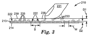
図2は、指231がタッチ面239にタッチしている状態のセンサ210の断面図を示す。上部の電極アレイ212は、ポリカーボネート、ポリエチレンテレフタレート(PET)、PMMA、ガラス、シリカ、若しくはこれらの組み合わせ(例えば、ガラスにコーティングされたシリカ)、PETハードコート材料、又は任意のその他の好適な材料で作製され得る上部基板238のそばのタッチ面239から、距離D1だけ離れている。非透明の容量式タッチパッドの場合、上部基板238は、コンピュータボードを作製するのに使用されるガラス繊維強化プラスチック(FRP)、又は任意のその他の好適な材料であることができる。図2に示されるセンサ構造では、上部の電極アレイ212は、下部基板213のそばの下部の電極アレイ214から距離D2だけ離れている。下部基板213は、上部基板238に用いられることができる材料のいずれか、又は任意のその他の適切な材料から作製されることができる。下部の電極アレイ214の電極(その1つの部材のみが図示されている)は、例えば、3つ以上の電極が、タッチしている指231と測定可能に容量接触することができる距離だけ、相互に離間され得る。例えば、下部の電極アレイ214は、5〜6mm、又は任意のその他所望の間隔の中心間間隔を有することができる。下部の電極アレイ214の電極の幅は、いくつかの実施形態において、電極間に最小限の非導電性スペースを残したいという要望によって、主に制約される。下部の電極アレイ214の電極は、指との容量結合を最大にするために、できるだけ幅広であることができる。例えば、下部基板213の表面積の90%以上、95%以上、又は98%以上を、下部の電極アレイ214で覆うことができる。
FIG. 2 shows a cross-sectional view of the
上部の電極は、上部の電極アレイ212の電極の間の下部の電極アレイ214の電極から、タッチしている(又は近接した)指までの電界結合が可能となるように離間される。上部の電極の幅(図2のW)は、例えば、中心間スペース間隔Sの50%以下であり得る。上部の電極アレイ212の電極がITOで作製される場合、それらの最小幅は多くの場合電極抵抗の制約を受ける。しかしながら、上部の電極アレイ212の電極は、薄いワイヤ、マイクロワイヤ、微小導体の相互接続ネットワーク、印刷微小導体、又は本開示と一致する任意のその他の構成及び任意の材料で作製される複合電極であることができる。
The upper electrodes are spaced so as to allow electric field coupling from the electrodes of the
図2において、長破線で示される電界232は、上部の電極アレイ212の電極が電気信号で作動された場合に、上部の電極アレイ212の電極と指231との間を結合する電界(E−field)を表している。この結合は、上部の電極アレイ212を含む複合電極のスペースを介して起こる。短破線で示される電界234は、上部の電極アレイ212の電極と、下部の電極アレイ214の電極との間の電界結合を表している。短破線で示される電界234のいくつかは、上部の電極アレイ212の電極の底面から下部の電極アレイ214の電極までを結合している。その他の電界の短破線234(特に指231に接近していない短破線)はフリンジフィールドを表しており、上部の電極アレイ212の電極の上面から上向きに結合し、下向きに曲がって下部の電極アレイ214の電極と交わる。指231の真下では、アレイ212の電極の上面から出る電界線は指231と結合する(指231に引き寄せられる)ので、電界線の極々少数だけが下部の電極アレイ214の電極と結合する。
In FIG. 2, an
上部の電極アレイ212の電極が電気信号によって作動されると、指231は、比較的低インピーダンスの人体とアース間の静電容量(例えば、400pf)でアースに接続され、下部の電極アレイ214の電極もまた寄生容量(例えば、100pf)でアースに接続される。これらは共に、指231をアレイ212又はアレイ214の電極のいずれかに結合する静電容量よりも有意に低いインピーダンスを有し、その範囲は、代表的な構成において、例えば、1pf〜5pfであり得る。これらの静電容量値は、上部の電極アレイ212及び下部の電極アレイ214の構成と共に、距離D1、D2、基板に使用される材料、並びに上部の電極アレイ212及び下部の電極アレイ214から図2に示されない接地面までの距離によって決まる。同様に、電気信号で下部の電極アレイ214の電極を作動させると、下部の電極アレイ214の電極から上部の電極アレイ212の電極を通って指231に至る電界が生成される。
When the electrodes of the
ここで図3を参照すると、長破線で示される電界233は、下部の電極アレイ214の電極と、上部の電極アレイ222の指231電極との間の電界結合を表している。図3において、上部の電極アレイ222の電極が、図2でのように複合電極ではなく、その代わりに従来の固体電極である点を除いて、図3は図2と同様である。電界線233は、主に下部アレイ214の電極から、上部の電極アレイ212の電極間のスペースを通って、指231までを結合する。短破線で示される電界235は、下部の電極アレイ214の電極と上部の電極アレイ222の電極との間の結合を表している。短破線235の一部は、下部の電極アレイ214の電極の上面から上部の電極アレイ222の電極の底面まで結合する。その他の短破線で示されるフリンジ電界235(特に指231に接近していない電界)は、下部の電極アレイ214の電極の上面から上向きに結合し、下向きに曲がって上部の電極アレイ222の電極の上面と交わる。長破線で示される電界233は、アレイ214の電極の上面が指231と直接結合しているのを表し、長破線で示される電界233の極少しだけが曲がって上部の電極アレイ222の電極の上部と結合する。
Referring now to FIG. 3, the
ここで留意すべきは、上部の電極アレイ222の電極が固体である場合、これら電極は下部の電極214からの電界を遮断するので、指231に結合する電界233は、主に上部の電極222間のスペースで生じることである。しかしながら、上部の電極が図2の複合電極212のように透過性である場合、これら電極は、電極構成体の間のスペースに電界を通過させる。
It should be noted here that when the electrodes of the
上部の電極アレイの電極(電極アレイ212又は222のいずれか)及び/又は下部の電極アレイ214は、図示されているように同時に作動される必要はないが、例示の目的で、上部の電極アレイ及び下部の電極アレイ214からの電極の電界を示している。
The electrodes of the upper electrode array (either
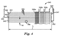
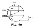
図4は、それぞれが幅Wを有する3つの上部の複合電極342、343、及び344を含む例示のタッチセンサ340を示す。複合電極342、343、及び344のそれぞれは、並列導体355(図4aの拡大図V1に示されており、複合電極の関係において相互導体(inter-conductors)と呼ばれることもある)を含む。複合電極342、343及び344は、各複合電極内の相互導体のスペースと幅が同じであり得るスペースによって分離される。伝導体の均一な間隔は、センサ全体に光学的均一性をもたらすことができ、したがって、伝導体は目に知覚されにくい。伝導体355は、例えば、一方若しくは両方の末端部、又は任意に中間的な位置(図4aの伝導体ブリッジ359)にある端部導体351及び352によって電気的に接続されて、複合電極を形成する。
FIG. 4 shows an
伝導体355は、10マイクロメートル未満、5マイクロメートル未満、いくつかの実施形態では3マイクロメートル未満の断面寸法を有することができる。このような直径を有する伝導体355は、対角線が1メートル未満のタッチ面などの透明なタッチ面を備える小さなディスプレイ上で伝導体が最小限に可視であるように、適切な光学性能をもたらすことができる。より大きな断面の伝導体を、場合によってはより大きな画素を有する、より大きなディスプレイ上で使用することができる。伝導体は、延伸されたワイヤ、マイクロワイヤであることができ、マイクロコンタクトプリントされる、マイクロカプセル化されることができ、又は任意のその他の適切な方法によって形成されることができる。マイクロコンタクトプリントされた伝導体は、幅およそ2マイクロメートル、厚さ100〜200ナノメートルであることができ、銀、金、又は同様の金属で作製されることができる。マイクロカプセル化された伝導体355は、約3マイクロメートル×3マイクロメートルの断面寸法を有することができ、銅又は同様の金属で作製されることができる。あるいは、微小導体は、銅又は同様の金属の延伸されたワイヤで作製されることができ、その断面寸法は、例えば、約10マイクロメートルであることができる。微小導体及びその作製方法は、本出願の中で後述される。
The
伝導体355間の間隔の寸法G1(図4a)は、50マイクロメートル〜4mmであることができる。一実施形態において、G1は0.5mm〜1mmであることができる。伝導体間のスペースは、複合電極342及び343の全長Lに及ぶことができ、又はスペースは、電極342に示されるように、若しくは参照により本明細書に組み込まれる米国特許出願第12/393,194号、「Touch Screen Sensor Having Varying Sheet Resistance」に記載のように、一定の又はランダムな間隔でコネクタブリッジ359を用いて短くされてもよい。最適な電気的性能を目的として、上部の複合電極342及び343の伝導体ブリッジ359は、間隔が存在するように(したがって電界が複合電極を通って立ち上がることができるように)最小限に抑えられる。多くの用途において、間隔の長さは、複合電極342、343、及び344の長さと同じ方向であるのが好ましいが、スペースの長さを複合電極342、343、及び344の長さと直交させるようにスペースを配置することも可能である。これらの原理が、並行線、又は円形、六角形、若しくは正方形の伝導体ネットワークなどの任意の他の形状にパターン化された伝導体のネットワークを含む電極に適用される。
The spacing dimension G1 (FIG. 4a) between the
電極358a、358b、及び358cは、3つの代替タイプの下部の電極である。図4の例示の実施形態では、これらは、複合電極342、343、及び344を含む平面の下の離れた平行面上にある。電極358aの伝導体は、相互接続された六角形の等方性ネットワーク状に配置され、これは、容量特性といくらかの遮断特性とを提供するが、電極358b(複合電極)のような並列導体の電極と比較すると、透明なタッチ面上でいくぶん可視であり得る。電極358cは透明なITOのフィルムで作製され、代表的な実施形態における抵抗率は約600オーム/平方以下である。電極358cは、通常、1MHz未満の周波数で良好な光学特性と良好な遮断特性とを有する。電極358bと複合電極342、343、及び344との交差位置では、伝導体は交点でのみで重なり合い、誘電体材料が交差位置の間の隙間を充填する。これは、電極358bと複合電極342、343、及び344との間の相互容量結合を最小限に抑える。電極358aは、伝導体の密度が高く、かつ電極358aの伝導体パターンに水平導体要素が存在するので、358bよりも大きな相互容量結合を有する。電極358cは、電極358a又は358bよりもより大きな相互容量結合を有する。
相互導体の間隔(例えばG1)が基板の厚さと比較して広く、したがって下の電極から電界が透過することを条件として、電極358a及び358bは上部の(透過性)複合電極で用いるのにも好適であり得る。並列導体を含む343、344、及び358bなどの複合電極はまた、参照により本明細書に組み込まれる米国特許出願第2007/0074914 A1号、「Interleaved Electrodes for Touch Sensing」に記載のように、挿入型電極構成で用いるのにも適している。
The
複合電極342、343、344及び358bのインピーダンス(抵抗及び容量の両方)は異方性であることができる。そのような場合、抵抗率(オーム/平方)は、典型的には、伝導体の配向の方向が最も低い。複合電極342、343、344及び358bにより生成される近傍電界(特に寸法G1の距離範囲内)は異方性であり、平行面上に近接して設置されたこのタイプの2つの電極の間の1平方メートル当たりの静電容量(C/M)は、電極の相対角度に依存し、平行電極は最大静電容量を引き起こし、直交電極は最小相互容量を引き起こす。導電性平板電極358cと異なり、複合電極342、343、344、358a、及び358bは、各電極内のネットワークの伝導体の間隔に応じた程度に電界透過性である。
The impedance (both resistance and capacitance) of the
透過性の上部の複合電極342、343、344の伝導体は、一実施形態において、マイクロワイヤと呼ばれる場合があり、共に参照により本明細書に組み込まれる、米国特許第5,512,131号、「Formation of Microstamped Patterns on Surfaces and Derivative Articles」、及び同第7,160,583号、「Microfabrication Using Patterned Topography and Self−Assembled Monolayers」に記載のマイクロコンタクトプリントによって製造されることができる。上部の複合電極342、343、344は、上部基板(図示せず)の上にマイクロコンタクトプリントされることができ、ガラス、PET、又は任意のその他の適切な材料で製造されることができる。別の方法としては、複合電極342、343、344は、マイクロコンタクトプリントによって下部基板(図示せず)に適用されることができる。下部の電極358a〜cは、(上述の)マイクロコンタクトプリントによって下部基板(図示せず)に適用されることができるか、若しくはマイクロカプセル化された伝導体は、例えば、参照により本明細書に組み込まれる米国特許出願第61/076731号、「Method of Forming a Microstructure」に開示されているように適用されてもよく、又はITO薄膜を使用することができる。あるいは、フレキシブルプリント基板上又は繊維強化プラスチック(即ち、PCB材料)上の銅伝導体を使用することができる。
The conductors of the transmissive upper
電界結合は、上部の複合電極アレイの各伝導体と、下部の電極アレイの各電極との間の静電容量を示す信号を、相互容量測定法及び当該技術分野において既知の回路を用いて測定することによって、測定され得る。図1〜図4に示されるもののようなマトリックスタッチセンサの場合、まず、ノードにおける上部の電極と下部の電極との間の相互容量を、任意のタッチが適用される前の測定することができ、未タッチと関連付けられた静電容量の値を、交差位置ごとに記録することができる。全ノードの静電容量を繰り返し測定し、タッチが発生したときに、1つ以上の交差位置の未タッチ状態とタッチ近似状態との間の静電容量の差異を計算する。タッチダウンは、一般的に、所定の閾値より大きい静電容量変化として確認される。プレタッチ(ホバー)もまた、異なる閾値を用いて確認されることができる。 Electric field coupling measures a signal indicating the capacitance between each conductor in the upper composite electrode array and each electrode in the lower electrode array using a mutual capacitance measurement method and circuitry known in the art. Can be measured. For matrix touch sensors such as those shown in FIGS. 1-4, first, the mutual capacitance between the upper and lower electrodes at a node can be measured before any touch is applied. The capacitance value associated with untouched can be recorded for each crossing position. The capacitance of all nodes is repeatedly measured, and when a touch occurs, the difference in capacitance between the untouched state and the touch approximate state at one or more intersection positions is calculated. Touchdown is generally confirmed as a capacitance change greater than a predetermined threshold. Pre-touch (hover) can also be confirmed using different thresholds.
複合電極の作製
図5aは、基板580上に並列導体550〜568を有するセンサ構成要素540の一部分を示す。一実施形態において、伝導体550〜568のそれぞれは、単一伝導体、若しくは複数の並列導体、又は図4に関して説明したような伝導体のネットワークを含む。伝導体550〜568は、相互に電気的に絶縁されている。基板580には、硬質ガラス若しくはPMMAシート、PETのロール、又は任意のその他の適切な材料を挙げることができる。例えば、伝導体550〜568との電気接触を形成するのが困難な場合には、容易に入手可能な導電性インクを使用して、任意の接触パッド579を基板540上の各伝導体に加えることができる。
Fabrication of Composite Electrode FIG. 5 a shows a portion of a
基板上に個々の伝導体を作製する様々な方法が、それぞれが参照により本明細書に組み込まれる、米国特許出願第12/393,185号(「Touch Screen Sensor」)、同第12/393,197号(「Touch Screen Sensor With Low Visibility Conductors」)、同第12/393,194号(「Touch Screen Sensor Having Varying Sheet Resistance」)、同第12/393,201号(「Methods of Patterning a Conductor on a Substrate」)、及び同第61/076,736号(「Method of Forming a Patterned Substrate」)に更に記載されている。参照により本明細書に組み込まれる米国特許第6,137,427号、「Multiple Input Proximity Detecto and Touchpad System」は、薄い銅ワイヤを含む伝導体の作製に関する更なる詳細を提供している。 Various methods of making individual conductors on a substrate are described in US patent application Ser. Nos. 12 / 393,185 (“Touch Screen Sensor”), 12/393, each incorporated herein by reference. No. 197 (“Touch Screen Sensor With Low Visibility Conductors”), No. 12/393, 194 (“Touch Screen Sensor Hasing varie ent”, No. 12 / No. a Substrate ") and 61 / 076,736 (" Method of Forming a Patterned Substr "). ate "). US Pat. No. 6,137,427, “Multiple Input Proximity Detect and Touchpad System”, incorporated herein by reference, provides further details regarding the fabrication of conductors comprising thin copper wires.
一実施形態において、本開示と一致するタッチセンサの作製方法の初期工程は、まず、一定距離だけ離間した並列導体550〜568を備える基板580を製造することである。基板580は、製造される最も大きなタッチセンサの長さ及び幅に適合するのに十分に大きい寸法を有することができるか、又は任意のその他の適切な寸法を有することができる。
In one embodiment, an initial step in a touch sensor fabrication method consistent with the present disclosure is to first manufacture a
伝導体550〜568を有する基板580を製造した後、選択した伝導体550〜568を共に電気的に結合して、図5b〜図5fに示されるような複合電極を形成することができる。伝導体550〜568は、基板540上に導体材料をコーティング又は印刷することによって、あるいは任意のその他の適切な方法によって接続され得る。例えば、センサ基板541(図5b)の構成に関し、端部導体570が伝導体550〜568及び基板580の上に印刷されて、それぞれが6つの伝導体からなる3つの複合電極を形成することができる。図5c及び図5dに示されるように、別の数の電極550〜568を端部導体572で接続することができる。任意の所望の数の電極を端部導体によって電気的に接続して、様々な構成の透過性複合電極を形成することができる。次に、端部導体は、コネクタに、又は相互接続部573a及びbを介して直接電子部品(図示せず)に、電気的に接続されることができる。別の方法としては、例えば、参照により本明細書に組み込まれる米国特許出願第2007/0030254 A1号、「Integration of Touch Sensors with Directly Mounted Electronic Components」に記載のように、端部導体570及び572は、伝導体550〜568の上に敷設され、かつ導電性インクで伝導体550〜568と電気的に接続されるプリント基板又はフレキシブルプリント回路の上に配置されることができる。図5eは、挿入型電極パターンを有するセンサ構成要素544の構成を示す。図5fのセンサ基板545の構成は、伝導体550〜558を有する基板580を含むセンサ構成要素545の例を示しており、各伝導体は、ワイヤのハチの巣状の構造で作製されている。伝導体550〜558は、端部導体575によって電気的に結合されて、複合電極を形成する。複合電極に電気的に結合される相互接続部573eは、電極を他の電気部品に接続する。
After manufacturing the
センサが2つ以上の層の電極を有する場合、両方の層は、同じ基板580から、又は異なる基板から作製され得る。例えば、マトリックスセンサは、電極の上部層を(下部の複合電極342、343、及び344に関して図4に示されるような)下層と積層することによって作製されることができる。あるいは、1組の電極は本明細書に記載のプロセスで作製されてよく、別の層の電極は、別のプロセスで、又はパターン化されたITO又は任意のその他の所望の材料などの異なる材料を使用して作製されてもよい。
If the sensor has more than one layer of electrodes, both layers can be made from the
形成されると、センサ構成要素(例えば図5b〜図5fに示される541、542、543、544及び545)は適当なサイズに切断され、上部及び下部電極層は共に積層されることができる。積層は切断に先行してもよく、又はその逆でもよい。 Once formed, the sensor components (eg, 541, 542, 543, 544 and 545 shown in FIGS. 5b-5f) can be cut to a suitable size and the upper and lower electrode layers can be laminated together. Lamination may precede cutting or vice versa.
本開示に従って作製されるセンサは、センサ製造時に、様々な形状、サイズ、及び構成にカスタマイズされることができる。例えば、図5aのセンサ構成要素540は、1mm又は任意のその他の適切な距離だけ離間した電極を有する基板580(例えば、PET)を含み得る。センサ構成要素540は、その後、図5b〜5fに示されるようなセンサ構成要素541、542、543、544、若しくは545のいずれか、又は所望のその他の構成を形成するように構成され得る。図5bのセンサ構成要素541は、幅5mmの電極を有し、図5cのセンサ構成要素542は、幅8mmの電極を有する。センサ構成要素543は、センサの縁部近くの位置補間を改善するために幅1mmの縁部の電極が使用される縁部を除き、幅5mmの電極を有する。「エッジバー」電極のその他の実施形態は、参照により本明細書に組み込まれる米国特許出願第2008/0252608 A1号、「Touch Sensor with Electrode Array」に記載されている。センサ構成要素544(図5e)もまた、縁部の電極575と、幅5mmの主電極とを有し、それぞれは、隣接する電極の外側電極に挟み込まれている2つの幅1mmの外側電極に接続される。上記電極間隔及び幅のそれぞれは、本開示に従って増大させる又は減少させることができる。
Sensors made in accordance with the present disclosure can be customized to various shapes, sizes, and configurations during sensor manufacture. For example, the
図6は、複数の並列導体605が複数のITO電極608の上方に配列されている代表的なマトリックスセンサ600の分解図を示す。例示される実施形態では、並列導体605及びITO電極608は互いに直交しているが、これらは任意の所望の角度であることができる。図6では、上部の並列導体605は、基板606の上に配置された36の分離した(電気的に結合しない)伝導体を含む。これら分離した伝導体のグループ(この例では伝導体6つずつ)は、基板620(例えば、プリント基板)の一部である端部導体621によって電気的に結合されて、複合伝導体を形成する。ITO電極608は、ガラス、PET、又は別の好適な材料であり得る基板610の上にコーティングされる。ITO電極608から基板625上の端部導体626までの電気的接続は、(6:1の割合を有する伝導体605のグループ化とは対照的に)1対1の割合を有する。端部導体626とITO電極608との間の電気的接続、及び端部導体621と伝導体605との間の電気的接続は、先に参照により本明細書に組み込まれた米国特許出願第11/377,976号、「Integration of Touch Sensors with Directly Mounted Electronic Components」に開示されている方法によって、又は任意のその他の適切な方法、例えば、銀をベースにした熱硬化された導電性インクによって行うことができる。
FIG. 6 shows an exploded view of an
マトリックスセンサ600の電気的接続は、マトリックスセンサの層を通ってビアを設けて、伝導体605又は電極608へのアクセスを提供することによって形成することもできる。電極608又は伝導体605の一部分を露出させて、はんだ、導体ペースト、コネクタ、又は連結部材などの導体材料でビアを充填することによって電気的接続を形成することが可能であり、これにより、伝導体605又は電極608は、接続部材への電気的接続で結合される。電極608又は伝導体605は、別の電子的構成要素若しくは装置に、又は指タッチの位置を判定するために使用される制御装置に、電気的に結合され得る。
The electrical connection of the
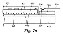
図7aは、「7a」と示されたセンサ600の部分の断面の分解されていない図を示す。下部基板610は、接着剤(図示せず)で、又は任意のその他の適切な方法によって取り付けられることによって、上部基板602に積層されることができる。電気的接続729は、センサの様々な構成要素をホストプロセッサ(図示せず)に接続する。
FIG. 7a shows an unexploded view of the cross section of the portion of the
図7bは、図7aに示されるものとの比較におけるセンサ600の代替構成を示す。具体的には、上部基板が除去され、下部基板720が上下逆になっているので、その上面がタッチ面となる。感圧性接着剤(PSA)のシートであり得る誘電体スペーサ722が、基板606と610との間に積層されている。
FIG. 7b shows an alternative configuration of the
タッチセンサ断面シミュレーション
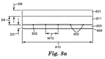
代表的なタッチセンサの断面におけるアースまでの静電容量の変化を、Ansoft Corp.(Pittsburgh,PA)から商標名「Maxwell Software」バージョン3.1.04で市販のシミュレータソフトウェアを使用してシミュレートした。図8a及び図8bは、このソフトウェアを使用してシミュレートされるタッチセンサの2つの設計の断面を示している。図8aは、本開示と一致する透過性の上部の複合電極を含み、図8bは、従来の上部の固体電極を有するタッチセンサの断面を示している。図8a及び図8bの両方において、指831(この実施例では、指831は食塩水の層としてシミュレートされている)は上部基板811と接触し、かつ下部の電極804と容量的に結合している。図8aには、伝導体802を均一に離間させた複合伝導体の断面が示されている。図8bには、固体電極822の断面が示されている。
Touch Sensor Cross Section Simulation A change in capacitance up to ground in a cross section of a typical touch sensor is shown in Ansoft Corp. (Pittsburgh, PA) under the trade name “Maxwell Software” version 3.1.04 was simulated using commercially available simulator software. Figures 8a and 8b show cross-sections of two designs of touch sensors that are simulated using this software. FIG. 8a includes a transparent upper composite electrode consistent with the present disclosure, and FIG. 8b shows a cross-section of a touch sensor having a conventional upper solid electrode. In both FIGS. 8 a and 8 b, the finger 831 (in this example, the
図8a及び図8bに対応するセンサに関する全ての試験では、特に記載のない限り、以下のパラメータが用いられた。 In all tests on the sensors corresponding to FIGS. 8a and 8b, the following parameters were used unless otherwise stated.

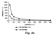
図9a及び図9bは、それぞれ上部及び下部の電極と、指831との間のシミュレートされた電界結合(静電容量)を示す。x軸は、上部基板811の厚さをマイクロメートルで示す。厚さの範囲は、ロール状のPETの一般的な厚さである50〜400マイクロメートル、及びPMMA硬質基板をシミュレートし得る0.4mmを含む。図9aは、シミュレートされた1Vの信号を上部の電極に有し、下部の電極は接地状態である(0ボルト)。図9bは、シミュレートされた1Vの信号を下部の電極に有し、上部の電極は接地状態である。
上述のように、図8bの上部の電極822の幅は550マイクロメートルであり、電極はシミュレートされる領域の半分を覆い、この寸法は一つにはシミュレーションを簡略化するために選択される。しかしながら、50%被覆率は、アースまでの静電容量を測定するために用いられる電流ITO電極の典型である。相互容量タッチシステム用の上部の電極は、センサの面積のわずか1%、2%、5%、10%、又は20%を覆うことができ、典型的な上部のITO複合電極の幅は1mm〜4mmの範囲内である。
As mentioned above, the width of the
図9aは、上部の電極802と指831との容量結合が、幅広の電極822と指831との結合未満であり、かつ基板の厚さが増大するにつれて両方の静電容量が減少することを示している。相互容量による方法を用いると、低い寄生容量は、通常、タッチに起因する静電容量の高い変化率をもたらす。
FIG. 9a shows that the capacitive coupling between the
図9bは、上部の電極が複合体である場合(図8a)と、固体である場合(図8b)の、下部の電極804から指831までの容量結合を比較している。このシミュレーションの間、上部の電極802及び822は0ボルトであるので、上部の電極は、下部の電極804から指831までを結合する電界の一部を遮断する。上部の透過性電極は、固体電極822と比べて、下部の電極804と指831との間の電界をほとんど遮断しないので、下部の電極804から指831までの結合を改善する。
FIG. 9b compares the capacitive coupling from the
図9cは、(上部の電極の)相互導体の間隔と、上部及び下部の電極104からの結合との関係を示す。このモデルは図8aに示されるセンサに基づいており、D3=D4=100マイクロメートル及びA10=1100マイクロメートルである。W10は、上部の電極伝導体の数が変わると変化する。図9cは、この実施例に関して、このシミュレーションで使用される伝導体では、複合伝導体を含む上部の電極伝導体が均等に約170マイクロメートル離間しているときに、タッチ機器から上部の電極までの容量結合は、下部の電極までの結合と等しいことを示している。一般に、複合電極を含む伝導体間の間隔は、電極からタッチ面までの距離の2倍未満であり得る。最適な伝導体の間隔は、センサ基板の誘電率によっても異なる。 FIG. 9 c shows the relationship between the mutual conductor spacing (of the upper electrode) and the coupling from the upper and lower electrodes 104. This model is based on the sensor shown in FIG. 8a, where D3 = D4 = 100 micrometers and A10 = 1100 micrometers. W10 changes as the number of upper electrode conductors changes. FIG. 9c shows, for this example, the conductor used in this simulation, from the touch device to the upper electrode when the upper electrode conductor, including the composite conductor, is evenly spaced about 170 micrometers apart. This indicates that the capacitive coupling is equal to the coupling to the lower electrode. In general, the spacing between conductors including composite electrodes can be less than twice the distance from the electrodes to the touch surface. The optimal conductor spacing also depends on the dielectric constant of the sensor substrate.
相互容量測定
図9dは、図8a及び図8bに関して示されたものに対応するシミュレートされたセンサにおける、上部の電極と下部の電極との間のシミュレートされた電界結合(相互容量)の結果を示す。PMMAを有する、及びガラスを有する上部基板811をシミュレートする。ガラスは、その耐久性のせいで好ましい場合があり、また、ガラスの誘電率は通常、PMMAの誘電率より高い。50〜100マイクロメートルの範囲内のガラスは、Schott Glass Company(Mainz,Germany)から入手可能である(例えば、Schott AF45ゼロアルカリ薄ガラス及びSchott 0211薄ガラス)。図9dは、指831が存在することによる、上部の電極伝導体と下部の電極伝導体との間の相互容量の変化を示す。電界の一部分が上部の電極伝導体から離れて指まで迂回するので、指831が存在する場合には相互容量は低減する。上部の電極の微小導体間の間隔が200マイクロメートルであることと、試験されるタッチ面の距離の範囲を考慮すると、伝導体で作られた電極をタッチしている間の相互容量変化は、固体電極よりもかなり大きい(負の傾斜が大きい)。
Mutual Capacitance Measurement FIG. 9d shows the result of simulated electric field coupling (mutual capacitance) between the upper and lower electrodes in a simulated sensor corresponding to that shown with respect to FIGS. 8a and 8b. Indicates. An
図9dはまた、上部基板が薄い場合に、伝導体で作られた上部の電極が相互容量式タッチの測定値をより改善することができることを示している。相互容量は、伝導体間の距離間隔及び上部基板の材料の誘電率に関連している。薄い上部基板では、(間のスペースが小さい)より多くの伝導体が最も良好に機能するが、厚い上部基板では、伝導体の間の距離間隔が広いほど(タッチに起因した変化率という点から見た)性能が改善される。寸法D4(図8a及び8b)が200マイクロメートル未満の場合に、シミュレートされた200マイクロメートルの上部基板厚さは最良の結果をもたらし、D4が最大約300マイクロメートルの場合に良好な性能をもたらす。上部の電極とタッチ面との間の厚さD4は、上部の電極の伝導体間の間隔の2倍未満で大きくてよい。 FIG. 9d also shows that when the top substrate is thin, the top electrode made of conductor can further improve the mutual touch measurement. Mutual capacitance is related to the distance between conductors and the dielectric constant of the material of the upper substrate. On a thin top substrate, more conductors work best (with a small space between them), but on a thick top substrate, the wider the distance between the conductors (in terms of the rate of change due to touch) Saw) performance is improved. When the dimension D4 (FIGS. 8a and 8b) is less than 200 micrometers, a simulated upper substrate thickness of 200 micrometers gives the best results, and good performance is achieved when D4 is up to about 300 micrometers. Bring. The thickness D4 between the upper electrode and the touch surface may be greater than less than twice the spacing between the conductors of the upper electrode.
更に、未タッチ状態にある図8aのセンサの上部の電極と下部の電極の間の相互容量の基本レベルは、基板811がPMMAで作られている場合には200pf、又は基板811がガラスで作られている場合には240pfである。これは、基板811がPMMAで作られている場合には約350pf、又は基板811がガラスで作られている場合には370pfである電極間の静電容量を有する図8bのセンサよりも、有意に低い。
Furthermore, the basic level of mutual capacitance between the upper and lower electrodes of the sensor of FIG. 8a in the untouched state is 200 pf if the
図9eは、タッチがある場合とない場合の、図8a及び図8bのセンサの上部の電極と下部の電極との間の静電容量の変化率を示す。高い静電容量変化と低い基本レベル(寄生)静電容量との組み合わせは、多くの微小導体からなる複合電極では、タッチと同時に有意に大きな信号変化をもたらす。 FIG. 9e shows the rate of change of capacitance between the upper and lower electrodes of the sensor of FIGS. 8a and 8b with and without touch. The combination of a high capacitance change and a low basic level (parasitic) capacitance results in a significantly large signal change at the same time as touch in a composite electrode consisting of many microconductors.
二次元タッチセンサシミュレーション
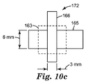
図10a、図10b及び図10cは、(図9a〜eの断面のモデルではなく)二次元電極のモデルの相互容量シミュレーションに使用されるセンサの概略を示す。同じシミュレーションソフトウェアを使用した。図10a、図10b及び図10cは、それぞれが、上部の電極を垂直に、下部の電極を水平に配向させて互いに直交配置された2つの電極(並びに、センサ配列170及び171の場合は、少なくとも1つの複合電極)を含む電極配置170、171、及び172をそれぞれ示す。複合電極161及び162はそれぞれ、直径0.18mmの4つの等間隔の平行な導電性ワイヤからなり、複合電極の全幅は6mmである。電極165及び166は、厚さ0.18mmの導電性シートである。導電性ワイヤ、導電性シート、及びタッチ手段は、シミュレーションを簡略化するための理想伝導体と近似させる。存在する場合、タッチ手段は、点線の正方形163で示される領域内の上部誘電体(オーバーレイ)層をタッチする。
Two-Dimensional Touch Sensor Simulation FIGS. 10a, 10b and 10c show a schematic of a sensor used for mutual capacitance simulation of a model of a two-dimensional electrode (rather than a cross-sectional model of FIGS. 9a-e). The same simulation software was used. FIGS. 10a, 10b and 10c each show two electrodes (and at least in the case of
センサ170及び171の断面図は、それぞれ図8a及び8bに関して示されたものと同様であり、底部にある下部の電極162又は165と、上部の電極と下部の電極との間の厚さ0.23mmのPETの誘電体(およその比誘電率=3)と、上部の電極161の上の厚さ0.23mmのPET(比誘電率=3)で作られた上部誘電体オーバーレイ層とを備える。いくつかのシミュレーションでは、誘電体オーバーレイに追加のガラス誘電体(比誘電率=6、厚さ=1mm又は2mm)を加えた。
The cross-sectional views of
図10cの断面図は、図8bに示されるものと同様であり、底部にある下部の電極165と、上部の電極と下部の電極との間の厚さ0.23mmのPETの誘電体(比誘電率=3)と、上部の電極166の上の厚さ0.23mmのPET(比誘電率=3)とを含む誘電体オーバーレイとを備える。いくつかのシミュレーションでは、誘電体オーバーレイに追加のガラス誘電体(比誘電率=6、厚さ=1mm又は2mm)を加えた。
The cross-sectional view of FIG. 10c is similar to that shown in FIG. 8b, with the
図11aは、3つの曲線を示すグラフである。各曲線のデータ点は、誘電体オーバーレイに接触しているタッチ手段を有する電極と、タッチ手段がない電極との間の相互容量(ΔCm)の差異を示す。曲線は、オーバーレイの異なる厚さに起因したΔCmの変化に対応するデータ点を結んでいる。上部誘電体のシミュレートされた厚さは以下の通りである:
・0.23mmのPET、
・0.23mmのPETに加えて1mmのガラス、及び
・0.23mmのPETに加えて2mmのガラス。
FIG. 11a is a graph showing three curves. The data points in each curve show the difference in mutual capacitance (ΔCm) between the electrode with touch means in contact with the dielectric overlay and the electrode without touch means. The curve connects data points corresponding to changes in ΔCm due to different overlay thicknesses. The simulated thickness of the top dielectric is as follows:
0.23 mm PET,
1 mm glass in addition to 0.23 mm PET, and 2 mm glass in addition to 0.23 mm PET.
図11aに関して示される曲線は、タッチによる相互容量変化が、厚い誘電体オーバーレイを有するセンサ配置172(図10c−固体の上部及び下部の電極)で最も大きいことを示している。固体電極の上に上部の透過性電極を備えるセンサ配置171(図10b)は、オーバーレイ厚さが比較的薄い(0.25mm未満)場合により大きな相互容量変化を有し、これは図9eに示される薄いオーバーレイに関するデータと一致する。センサ配置170(図10a−透過性の上部及び下部の電極)は、タッチによる相互容量変化が最も小さい。 The curve shown with respect to FIG. 11a shows that the mutual capacitance change due to touch is greatest for sensor arrangement 172 (FIG. 10c—solid top and bottom electrodes) with a thick dielectric overlay. The sensor arrangement 171 (FIG. 10b) with the upper transmissive electrode on top of the solid electrode has a larger mutual capacitance change when the overlay thickness is relatively thin (less than 0.25 mm), which is shown in FIG. 9e. Consistent with data on thin overlays. The sensor arrangement 170 (FIG. 10a—transparent upper and lower electrodes) has the least mutual capacitance change due to touch.
図11bは、センサ配置170(図10a)が、2つの電極間の相互の寄生容量の非常に低い(約0.12pf)静電気レベルに起因して、相互容量の最も大きな変化率を有することを示すグラフである。センサ配置172(図10c)は、電極165及び166の交差位置でごく近接する2つのコンデンサプレートによってもたらされる大きな相互の寄生容量(約2.5pf)に起因して、最も低い変化率を有する。センサ配置171(図10b)の複合電極は、寄生容量を約0.75pfまで最小にし、その結果、オーバーレイ厚さに応じて、タッチによる相互容量の変化は8%〜32%となる。
FIG. 11b shows that the sensor arrangement 170 (FIG. 10a) has the greatest rate of change of mutual capacitance due to a very low (about 0.12 pf) electrostatic level of mutual parasitic capacitance between the two electrodes. It is a graph to show. The sensor arrangement 172 (FIG. 10c) has the lowest rate of change due to the large mutual parasitic capacitance (about 2.5 pf) provided by two capacitor plates in close proximity at the intersection of
検出の近接性(指が電極間の相互容量を低減する距離)は、(図8aの距離D4に関して上述した)複合電極内の伝導体の距離間隔に比例する。これは、指が非常に近くに来る又はタッチ面と接触するまでタッチが検出されないのを確実にすることを助けるのに有利に用いることができる。 The proximity of detection (distance that the finger reduces the mutual capacitance between the electrodes) is proportional to the distance distance of the conductors in the composite electrode (described above with respect to distance D4 in FIG. 8a). This can be advantageously used to help ensure that no touch is detected until the finger is very close or touches the touch surface.
本特許出願は、タッチセンサに接近する指の検出及び位置付けに関する。本発明は指の検出に限定されない。本明細書に開示された装置及び方法を用いて、ほとんどどの導電性材料で作製された用具も検出されることができる。タッチに用いられる指又は導電性物体は、特に指定のない限り、静電容量及び/又は抵抗(典型的には数百〜数千ピコファラッド)によってアースに接続される。 This patent application relates to detection and positioning of a finger approaching a touch sensor. The present invention is not limited to finger detection. Using the devices and methods disclosed herein, tools made of almost any conductive material can be detected. Fingers or conductive objects used for touch are connected to ground by capacitance and / or resistance (typically hundreds to thousands of picofarads) unless otherwise specified.
Claims (25)
複数のマイクロワイヤ伝導体からなる複数の複合電極を含む上部電極層と、
複数の電極を含む下部電極層であって、上部の前記電極及び下部の前記電極は、該上部の電極及び該下部の電極が交差するノードを有する電極マトリックスを画定し、前記上部電極層は前記第1の層と前記下部電極層との間に配置される、下部電極層と、
前記上部電極層と前記下部電極層との間に配置される誘電体層と、
を備える、多層タッチパネル。 A first layer comprising a transparent touch surface;
An upper electrode layer comprising a plurality of composite electrodes made of a plurality of microwire conductors;
A lower electrode layer comprising a plurality of electrodes, wherein the upper electrode and the lower electrode define an electrode matrix having nodes where the upper electrode and the lower electrode intersect, and the upper electrode layer A lower electrode layer disposed between the first layer and the lower electrode layer;
A dielectric layer disposed between the upper electrode layer and the lower electrode layer;
A multi-layer touch panel.
前記上部電極層の電極と前記下部電極層の電極との間の静電容量を示す信号を感知するように構成される受信回路と、
を更に備える、請求項1に記載の多層タッチパネル。 A drive circuit configured to electrically drive at least one of the lower electrodes;
A receiving circuit configured to sense a signal indicative of a capacitance between an electrode of the upper electrode layer and an electrode of the lower electrode layer;
The multilayer touch panel according to claim 1, further comprising:
前記下部電極層の前記少なくとも1つの電極とアース基準電圧との間の静電容量を示す信号を感知するように構成される受信回路と、
を更に備える、請求項1に記載の多層タッチパネル。 A drive circuit configured to electrically drive at least one electrode of the upper electrode layer;
A receiver circuit configured to sense a signal indicative of a capacitance between the at least one electrode of the lower electrode layer and a ground reference voltage;
The multilayer touch panel according to claim 1, further comprising:
電子制御装置を用いてマトリックスタイプのタッチセンサに配置された重なっている上部の電極と下部の電極との間の、前記タッチセンサに近接する物体の存在によって誘発される相互容量の変化を示す値を感知することを含み、前記上部の電極が、複数のマイクロワイヤ伝導体からなる複合電極である、方法。 A method for identifying the location of a touch or an event close to a touch on a touch sensing device comprises:
A value indicating the change in mutual capacitance induced by the presence of an object proximate to the touch sensor between the overlapping upper and lower electrodes disposed on the matrix type touch sensor using an electronic control device And the upper electrode is a composite electrode comprised of a plurality of microwire conductors.
Applications Claiming Priority (3)
| Application Number | Priority Date | Filing Date | Title |
|---|---|---|---|
| US8569308P | 2008-08-01 | 2008-08-01 | |
| US61/085,693 | 2008-08-01 | ||
| PCT/US2009/052070 WO2010014683A2 (en) | 2008-08-01 | 2009-07-29 | Touch sensitive devices with composite electrodes |
Publications (1)
| Publication Number | Publication Date |
|---|---|
| JP2011530113A true JP2011530113A (en) | 2011-12-15 |
Family
ID=41607845
Family Applications (2)
| Application Number | Title | Priority Date | Filing Date |
|---|---|---|---|
| JP2011521271A Expired - Fee Related JP5753084B2 (en) | 2008-08-01 | 2009-07-29 | Manufacturing method of composite electrode |
| JP2011521273A Withdrawn JP2011530113A (en) | 2008-08-01 | 2009-07-29 | Touch sensing device with composite electrode |
Family Applications Before (1)
| Application Number | Title | Priority Date | Filing Date |
|---|---|---|---|
| JP2011521271A Expired - Fee Related JP5753084B2 (en) | 2008-08-01 | 2009-07-29 | Manufacturing method of composite electrode |
Country Status (7)
| Country | Link |
|---|---|
| US (3) | US8279187B2 (en) |
| EP (2) | EP2327007A4 (en) |
| JP (2) | JP5753084B2 (en) |
| KR (2) | KR101665148B1 (en) |
| CN (3) | CN103713771B (en) |
| TW (2) | TWI484399B (en) |
| WO (2) | WO2010014679A2 (en) |
Cited By (8)
| Publication number | Priority date | Publication date | Assignee | Title |
|---|---|---|---|---|
| JP2010250770A (en) * | 2009-04-20 | 2010-11-04 | Sony Corp | Information input device and display device |
| JP2011070659A (en) * | 2009-09-24 | 2011-04-07 | Chi Mei Electronics Corp | Capacitive type touch panel |
| JP2012094115A (en) * | 2010-09-30 | 2012-05-17 | Fujifilm Corp | Electrostatic capacitive touch panel |
| JP2013152599A (en) * | 2012-01-25 | 2013-08-08 | Fujifilm Corp | Conductive sheet and method for inspecting the same and method for manufacturing the same |
| JP2013531778A (en) * | 2010-04-15 | 2013-08-08 | オーセンテック,インコーポレイテッド | Finger sensor including capacitive lens and method related thereto |
| JP2013161448A (en) * | 2012-02-08 | 2013-08-19 | Dainippon Printing Co Ltd | Touch panel sensor, display device with touch panel and method of manufacturing touch panel sensor |
| JP2013186632A (en) * | 2012-03-07 | 2013-09-19 | Toppan Printing Co Ltd | Film-like touch panel sensor and manufacturing method thereof |
| JP2014032438A (en) * | 2012-08-01 | 2014-02-20 | Japan Display Inc | Input device and display device with input device |
Families Citing this family (184)
| Publication number | Priority date | Publication date | Assignee | Title |
|---|---|---|---|---|
| TW201005613A (en) * | 2008-04-10 | 2010-02-01 | Atmel Corp | Capacitive position sensor |
| JP5229887B2 (en) * | 2008-08-06 | 2013-07-03 | 株式会社ワコム | Position detection device |
| US8269744B2 (en) * | 2008-09-05 | 2012-09-18 | Mitsubishi Electric Corporation | Touch screen, touch panel and display device |
| KR101022143B1 (en) * | 2009-01-16 | 2011-03-17 | 삼성모바일디스플레이주식회사 | Touch Screen Panel |
| JP5643774B2 (en) | 2009-02-26 | 2014-12-17 | スリーエム イノベイティブ プロパティズ カンパニー | TOUCH SCREEN SENSOR AND PATTERN SUBSTRATE HAVING OVER-MINIMUM PATTERN WITH LOW VISibility |
| US9024907B2 (en) * | 2009-04-03 | 2015-05-05 | Synaptics Incorporated | Input device with capacitive force sensor and method for constructing the same |
| WO2011002617A1 (en) | 2009-06-30 | 2011-01-06 | 3M Innovative Properties Company | Electronic displays and metal micropatterned substrates having a graphic |
| US8279197B2 (en) * | 2009-08-25 | 2012-10-02 | Pixart Imaging Inc. | Method and apparatus for detecting defective traces in a mutual capacitance touch sensing device |
| KR101073684B1 (en) * | 2009-08-25 | 2011-10-14 | 주식회사 지니틱스 | Transparent Electrode Pattern Of Capacitive Touch Screen For Low Resistance |
| US8599150B2 (en) | 2009-10-29 | 2013-12-03 | Atmel Corporation | Touchscreen electrode configuration |
| JP5347913B2 (en) * | 2009-11-06 | 2013-11-20 | ソニー株式会社 | SENSOR DEVICE, ELECTRONIC DEVICE, AND METHOD FOR MANUFACTURING SENSOR DEVICE |
| JP5676645B2 (en) | 2009-12-29 | 2015-02-25 | クォルコム・メムズ・テクノロジーズ・インコーポレーテッド | Coated light redirecting lighting device with auxiliary electrode structure |
| KR101085776B1 (en) * | 2010-01-15 | 2011-11-21 | 삼성전자주식회사 | Touch panel and device for recognizing input using the touch panel |
| CN201622554U (en) * | 2010-02-04 | 2010-11-03 | 深圳市汇顶科技有限公司 | Capacitance touch sensor, touch detection device, and touch control terminal |
| FI20105155A (en) * | 2010-02-17 | 2011-08-18 | Marimils Oy | Method for detecting objects in a surface sensor system and surface sensor system |
| US9057653B2 (en) * | 2010-05-11 | 2015-06-16 | Synaptics Incorporated | Input device with force sensing |
| TWI419024B (en) * | 2010-05-17 | 2013-12-11 | Prime View Int Co Ltd | Touch display apparatus and electronic reading apparatus with touch inputting function |
| KR101093651B1 (en) * | 2010-05-25 | 2011-12-15 | 전자부품연구원 | Touch panel using metallic thin-film and manufacture method thereof |
| US20120013565A1 (en) | 2010-07-16 | 2012-01-19 | Perceptive Pixel Inc. | Techniques for Locally Improving Signal to Noise in a Capacitive Touch Sensor |
| US8766931B2 (en) | 2010-07-16 | 2014-07-01 | Perceptive Pixel Inc. | Capacitive touch sensor having code-divided and time-divided transmit waveforms |
| US8519970B2 (en) | 2010-07-16 | 2013-08-27 | Perceptive Pixel Inc. | Capacitive touch sensor having correlation with a receiver |
| US8599165B2 (en) * | 2010-08-16 | 2013-12-03 | Perceptive Pixel Inc. | Force and true capacitive touch measurement techniques for capacitive touch sensors |
| US8315058B2 (en) | 2010-09-14 | 2012-11-20 | Rosemount Inc. | Capacitive touch interface assembly |
| TWI427521B (en) * | 2010-09-15 | 2014-02-21 | Au Optronics Corp | Capacitive touch sensor and capacitive touch apparatus |
| JP5563417B2 (en) * | 2010-09-30 | 2014-07-30 | 株式会社ジャパンディスプレイ | Display device with touch panel |
| JP5645581B2 (en) | 2010-10-05 | 2014-12-24 | 富士フイルム株式会社 | Touch panel |
| US10185446B2 (en) | 2010-10-15 | 2019-01-22 | Apple Inc. | Touch sensor arrays with integrated inter-layer contacts |
| KR101646616B1 (en) * | 2010-11-30 | 2016-08-12 | 삼성전자주식회사 | Apparatus and Method for Controlling Object |
| US8405627B2 (en) * | 2010-12-07 | 2013-03-26 | Sony Mobile Communications Ab | Touch input disambiguation |
| KR101230191B1 (en) * | 2010-12-14 | 2013-02-06 | 삼성디스플레이 주식회사 | Touch Screen Panel and Fabricating Method for the Same |
| KR101473132B1 (en) | 2011-01-18 | 2014-12-15 | 후지필름 가부시키가이샤 | Transparent electrode sheets, manufacturing method for transparent electrode sheets, and capacitive touch panel using transparent electrode sheets |
| US20120188208A1 (en) * | 2011-01-20 | 2012-07-26 | Breit Solutions, LLC | Interface enhancement component for use with electronic touch-screen devices |
| US8619047B2 (en) | 2011-02-04 | 2013-12-31 | Perceptive Pixel Inc. | Techniques for disambiguating touch data |
| US8658917B2 (en) | 2011-02-04 | 2014-02-25 | Perceptive Pixel Inc. | Techniques for disambiguating touch data using user devices |
| KR101181342B1 (en) * | 2011-02-16 | 2012-09-11 | 에쓰이에이치에프코리아 (주) | Touch screen |
| CN103380411B (en) * | 2011-02-24 | 2016-10-05 | 富士胶片株式会社 | Conducting strip and contact panel |
| JP5968922B2 (en) | 2011-03-02 | 2016-08-10 | パーセプティブ ピクセル インコーポレイテッド | Noise reduction in touch sensors |
| US9557857B2 (en) | 2011-04-26 | 2017-01-31 | Synaptics Incorporated | Input device with force sensing and haptic response |
| US9152288B2 (en) * | 2011-05-19 | 2015-10-06 | Microsoft Technology Licensing, Llc | Remote multi-touch |
| US20120299865A1 (en) * | 2011-05-25 | 2012-11-29 | Hyunseok Yu | Sensor for Capacitive Touch Panel Including Mesh Pattern and Capacitive Touch Panel Including the Same |
| CN103597431B (en) * | 2011-06-09 | 2017-03-22 | 3M创新有限公司 | Touch sensitive device with multilayer electrode and underlayer |
| TWI450145B (en) * | 2011-06-14 | 2014-08-21 | Wintek Corp | Touch-sensing apparatus and touch-sensing display apparatus |
| WO2013008826A1 (en) | 2011-07-11 | 2013-01-17 | 富士フイルム株式会社 | Conductive sheet, touch panel, display device, method for producing said conductive sheet, and recording medium |
| US9501179B2 (en) * | 2011-08-04 | 2016-11-22 | Atmel Corporation | Touch sensor for curved or flexible surfaces |
| TW201310470A (en) * | 2011-08-31 | 2013-03-01 | Shih Hua Technology Ltd | Transparent conductive film and touch panel using the same |
| US9748952B2 (en) | 2011-09-21 | 2017-08-29 | Synaptics Incorporated | Input device with integrated deformable electrode structure for force sensing |
| US9612265B1 (en) | 2011-09-23 | 2017-04-04 | Cypress Semiconductor Corporation | Methods and apparatus to detect a conductive object |
| JP5822637B2 (en) | 2011-10-12 | 2015-11-24 | 三菱電機株式会社 | Touch panel and display device including the same |
| US9041418B2 (en) | 2011-10-25 | 2015-05-26 | Synaptics Incorporated | Input device with force sensing |
| US8963561B2 (en) | 2011-11-03 | 2015-02-24 | Atmel Corporation | Randomizing one or more micro-features of a touch sensor |
| KR20130051803A (en) * | 2011-11-10 | 2013-05-21 | 삼성전기주식회사 | Touch panel |
| US20130127784A1 (en) * | 2011-11-22 | 2013-05-23 | Qualcomm Mems Technologies, Inc. | Methods and apparatuses for hiding optical contrast features |
| US9262019B2 (en) * | 2011-11-22 | 2016-02-16 | Atmel Corporation | Touch sensor with conductive lines having different widths |
| US9095058B2 (en) * | 2011-11-30 | 2015-07-28 | Touchsensor Technologies, Llc | Electrode structure with spatial interpolation for capacitive touch panel |
| US9323092B2 (en) | 2011-12-05 | 2016-04-26 | Htc Corporation | Touch panel |
| US9634660B2 (en) * | 2011-12-20 | 2017-04-25 | Atmel Corporation | Touch sensor with reduced anti-touch effects |
| DE102011122110B4 (en) * | 2011-12-22 | 2023-05-25 | Polyic Gmbh & Co. Kg | Operating device with display device and touch panel device, and multi-layer body for providing a touch panel functionality |
| US8910104B2 (en) * | 2012-01-23 | 2014-12-09 | Cirque Corporation | Graduated routing for routing electrodes coupled to touch sensor electrodes to thereby balance capacitance on the touch sensor electrodes |
| JP5831262B2 (en) * | 2012-02-01 | 2015-12-09 | 三菱電機株式会社 | Touch screen, touch panel, and display device including the same |
| US9817523B2 (en) * | 2012-02-09 | 2017-11-14 | Qualcomm Incorporated | Capacitive touch panel for mitigating and/or exaggerating floating condition effects |
| WO2013119308A1 (en) | 2012-02-10 | 2013-08-15 | 3M Innovative Properties Company | Mesh patterns for touch sensor electrodes |
| US9081442B2 (en) | 2012-02-27 | 2015-07-14 | Apple Inc. | Split sense lines for negative pixel compensation |
| US8937604B2 (en) | 2012-02-28 | 2015-01-20 | Eastman Kodak Company | Touch-responsive capacitor with polarizing dielectric structure |
| US8836668B2 (en) | 2012-02-28 | 2014-09-16 | Eastman Kodak Company | Transparent touch-responsive capacitor with variable-height micro-wires |
| US9282647B2 (en) | 2012-02-28 | 2016-03-08 | Eastman Kodak Company | Method of making micro-channel structure for micro-wires |
| US8773393B2 (en) * | 2012-02-28 | 2014-07-08 | Eastman Kodak Company | Touch screen with dummy micro-wires |
| US8884918B2 (en) | 2012-02-28 | 2014-11-11 | Eastman Kodak Company | Electronic device having metallic micro-wires |
| US9046974B2 (en) * | 2012-02-28 | 2015-06-02 | Eastman Kodak Company | Transparent touch-screen capacitor with micro-wire electrode |
| US8661662B1 (en) | 2012-08-10 | 2014-03-04 | Eastman Kodak Company | Making transparent touch-responsive device with micro-wire electrodes |
| US8819927B2 (en) | 2012-02-28 | 2014-09-02 | Eastman Kodak Company | Method of making a transparent conductor structure |
| US8943682B2 (en) | 2012-02-28 | 2015-02-03 | Eastman Kodak Company | Making micro-wires with different heights |
| US8952263B2 (en) | 2012-08-10 | 2015-02-10 | Eastman Kodak Company | Micro-wire electrode pattern |
| US8773392B2 (en) | 2012-02-28 | 2014-07-08 | Eastman Kodak Company | Transparent touch-responsive capacitor with variable-pattern micro-wires |
| US8865292B2 (en) | 2013-01-22 | 2014-10-21 | Eastman Kodak Company | Micro-channel structure for micro-wires |
| US9154127B2 (en) * | 2012-03-06 | 2015-10-06 | Atmel Corporation | Touch sensor with conductive lines having portions with different widths |
| US8860692B2 (en) * | 2012-03-23 | 2014-10-14 | Zinitix Co., Ltd. | Touch pad and method for detecting multi-touch using the same |
| US9430107B2 (en) | 2012-03-30 | 2016-08-30 | Microchip Technology Incorporated | Determining touch locations and forces thereto on a touch and force sensing surface |
| US9207820B2 (en) * | 2012-03-30 | 2015-12-08 | Microchip Technology Incorporated | Method and system for multi-touch decoding |
| US8773395B2 (en) | 2012-04-24 | 2014-07-08 | Eastman Kodak Company | Touch-responsive capacitor with polarizing dielectric method |
| GB2502600B8 (en) | 2012-05-31 | 2015-01-07 | Improvements in touch sensitive displays | |
| GB2502601A (en) * | 2012-05-31 | 2013-12-04 | Zytronic Displays Ltd | A touch sensitive panel made with individually insulated wires |
| JP2014010671A (en) * | 2012-06-29 | 2014-01-20 | Mitsubishi Electric Corp | Touch screen, touch panel and display device including the same |
| TWI470476B (en) * | 2012-07-19 | 2015-01-21 | Wistron Corp | Electric device with proximity sense structure and proximity sense structure. |
| CN103294293B (en) * | 2012-07-27 | 2016-04-06 | 上海天马微电子有限公司 | The touch-control graphic structure of embedded capacitive touch screen |
| US9477352B2 (en) | 2012-08-10 | 2016-10-25 | Eastman Kodak Company | Making display device with pixel-aligned micro-wire electrode |
| US9030438B2 (en) | 2012-08-16 | 2015-05-12 | Eastman Kodak Company | Pixel-aligned micro-wire electrode device |
| US9098154B2 (en) * | 2012-08-10 | 2015-08-04 | Eastman Kodak Company | Display apparatus with pixel-aligned micro-wire electrode |
| US9005744B2 (en) | 2012-08-10 | 2015-04-14 | Eastman Kodak Company | Conductive micro-wire structure |
| US9052788B2 (en) | 2012-08-10 | 2015-06-09 | Eastman Kodak Company | Touch detection for capacitive touch screen |
| US9167688B2 (en) | 2012-08-10 | 2015-10-20 | Eastman Kodak Company | Micro-wire pattern for electrode connection |
| US9131606B2 (en) | 2012-08-10 | 2015-09-08 | Eastman Kodak Company | Micro-channel pattern for effective ink distribution |
| US8585455B1 (en) | 2012-09-26 | 2013-11-19 | Eastman Kodak Company | Making display device with pixel-aligned ground micro-wire |
| US8854327B2 (en) | 2012-09-26 | 2014-10-07 | Eastman Kodak Company | Display apparatus with pixel-aligned ground micro-wire |
| US9024918B2 (en) * | 2012-08-16 | 2015-05-05 | Eastman Kodak Company | Display apparatus with pixel-aligned electrode |
| US9244558B2 (en) | 2012-08-16 | 2016-01-26 | Eastman Kodak Company | Pixel-aligned electrode device |
| US9134860B2 (en) * | 2012-08-16 | 2015-09-15 | Eastman Kodak Company | Method of making a display device |
| US9092088B2 (en) | 2012-08-16 | 2015-07-28 | Eastman Kodak Company | Pixel-aligned ground micro-wire device |
| TWI465986B (en) * | 2012-09-17 | 2014-12-21 | Au Optronics Corp | Touch panel and touch display panel |
| US9164630B2 (en) | 2012-09-26 | 2015-10-20 | Eastman Kodak Company | Display apparatus with pixel-aligned ground mesh |
| US8591279B1 (en) * | 2012-10-19 | 2013-11-26 | Eastman Kodak Company | Making display apparatus with pixel-aligned ground mesh |
| JP5607697B2 (en) * | 2012-10-16 | 2014-10-15 | 日本写真印刷株式会社 | Touch sensor and electronic device |
| TWI592843B (en) * | 2012-11-09 | 2017-07-21 | 恆顥科技股份有限公司 | Touch electrode device |
| CN103116426A (en) * | 2012-11-20 | 2013-05-22 | 漳州宝发光电科技有限公司 | Composite material type touch screen and production technology thereof |
| US9164607B2 (en) | 2012-11-30 | 2015-10-20 | 3M Innovative Properties Company | Complementary touch panel electrodes |
| TWI552211B (en) * | 2012-11-30 | 2016-10-01 | 恆顥科技股份有限公司 | Touch electrode device |
| US9229553B2 (en) | 2012-11-30 | 2016-01-05 | 3M Innovative Properties Company | Mesh patterns for touch sensor electrodes |
| EP2929544A4 (en) | 2012-12-07 | 2016-07-06 | 3M Innovative Properties Co | Electrically conductive articles |
| BR112015013033A2 (en) * | 2012-12-07 | 2017-07-11 | 3M Innovative Properties Co | method of manufacturing transparent conductors on substrate |
| CN103870035B (en) * | 2012-12-10 | 2017-02-22 | 深圳欧菲光科技股份有限公司 | Touch sensing element and touch screen |
| US20140216783A1 (en) * | 2013-02-05 | 2014-08-07 | David P. Trauernicht | Micro-wire pattern with offset intersections |
| CN103064576B (en) * | 2013-02-07 | 2015-08-05 | 汕头超声显示器(二厂)有限公司 | A kind of capacitance touch screen with nano silver electrode |
| US9061463B2 (en) | 2013-02-28 | 2015-06-23 | Eastman Kodak Company | Embossed micro-structure with cured transfer material method |
| US9304636B2 (en) * | 2013-09-20 | 2016-04-05 | Eastman Kodak Company | Micro-wire touch screen with unpatterned conductive layer |
| US8932474B1 (en) | 2013-03-05 | 2015-01-13 | Eastman Kodak Company | Imprinted multi-layer micro structure method |
| US9167700B2 (en) * | 2013-03-05 | 2015-10-20 | Eastman Kodak Company | Micro-channel connection method |
| US9085194B2 (en) | 2013-03-05 | 2015-07-21 | Eastman Kodak Company | Embossing stamp for optically diffuse micro-channel |
| US8895429B2 (en) | 2013-03-05 | 2014-11-25 | Eastman Kodak Company | Micro-channel structure with variable depths |
| US20140308435A1 (en) | 2013-04-15 | 2014-10-16 | Mitchell Stewart Burberry | Hybrid single-side touch screen method |
| US20150085456A1 (en) | 2013-03-05 | 2015-03-26 | Ronald Steven Cok | Imprinted multi-level micro-wire circuit structure |
| US9229260B2 (en) | 2013-04-15 | 2016-01-05 | Eastman Kodak Company | Imprinted bi-layer micro-structure |
| USD742841S1 (en) * | 2013-03-26 | 2015-11-10 | Sony Corporation | Touch sensitive device |
| JP6245257B2 (en) * | 2013-04-04 | 2017-12-13 | ソニー株式会社 | Input device and electronic device |
| US20140307178A1 (en) * | 2013-04-12 | 2014-10-16 | Shenzhen O-Film Tech Co., Ltd | Touch screen sensing module, manufacturing method thereof and display device |
| KR101452747B1 (en) * | 2013-04-24 | 2014-10-23 | 한국표준과학연구원 | Capacitive touch panel with improved sensitivity of proximity, location and intensity of force of multi-touch input, method measuring thereof and method manufacturing thereof |
| DE102013104644B4 (en) | 2013-05-06 | 2020-06-04 | Polylc Gmbh & Co. Kg | Layer electrode for touch screens |
| US9871544B2 (en) | 2013-05-29 | 2018-01-16 | Microsoft Technology Licensing, Llc | Specific absorption rate mitigation |
| US10893488B2 (en) | 2013-06-14 | 2021-01-12 | Microsoft Technology Licensing, Llc | Radio frequency (RF) power back-off optimization for specific absorption rate (SAR) compliance |
| KR101717983B1 (en) * | 2013-07-05 | 2017-03-21 | 주식회사 잉크테크 | Method for making conductive transparent substrate and conductive transparent substrate |
| JP5943023B2 (en) * | 2013-07-08 | 2016-06-29 | 凸版印刷株式会社 | Touch sensor electrode, touch panel, and display device |
| KR102053258B1 (en) * | 2013-07-16 | 2019-12-06 | 엘지이노텍 주식회사 | Touch window |
| TWI509491B (en) * | 2013-07-23 | 2015-11-21 | Htc Corp | Touch panel |
| KR102142855B1 (en) * | 2013-08-29 | 2020-08-31 | 미래나노텍(주) | Wired electrode for touchscreen panel, touchscreen panel using the same and manufacturing method of the same |
| CN104423738A (en) * | 2013-08-30 | 2015-03-18 | 天津富纳源创科技有限公司 | Control method of capacitive touch device |
| CN104423737A (en) * | 2013-08-30 | 2015-03-18 | 天津富纳源创科技有限公司 | Capacitive touch device and control method |
| US8872526B1 (en) * | 2013-09-10 | 2014-10-28 | Cypress Semiconductor Corporation | Interleaving sense elements of a capacitive-sense array |
| KR20150029507A (en) * | 2013-09-10 | 2015-03-18 | 미래나노텍(주) | Touch screen sensor, Touch screen panel of electrostatic capacitive type and image display device |
| US9448674B2 (en) | 2013-09-11 | 2016-09-20 | Eastman Kodak Company | Making multi-layer micro-wire structure |
| US9465501B2 (en) | 2013-09-11 | 2016-10-11 | Eastman Kodak Company | Multi-layer micro-wire substrate method |
| US9513759B2 (en) | 2013-09-11 | 2016-12-06 | Eastman Kodak Company | Multi-layer micro-wire structure |
| US9107316B2 (en) | 2013-09-11 | 2015-08-11 | Eastman Kodak Company | Multi-layer micro-wire substrate structure |
| KR102120776B1 (en) * | 2013-09-16 | 2020-06-11 | 주식회사 리딩유아이 | Touch panel |
| JP5795038B2 (en) | 2013-10-01 | 2015-10-14 | 日本写真印刷株式会社 | Electrode sheet for capacitive touch panel |
| KR101512568B1 (en) | 2013-12-24 | 2015-04-15 | 삼성전기주식회사 | Touch panel and touchscreen apparatus including the same |
| KR20150074350A (en) | 2013-12-24 | 2015-07-02 | 삼성전기주식회사 | Touch panel and touchscreen apparatus including the same |
| US9563316B2 (en) | 2014-01-10 | 2017-02-07 | Microsoft Technology Licensing, Llc | Radiofrequency-wave-transparent capacitive sensor pad |
| US10044095B2 (en) | 2014-01-10 | 2018-08-07 | Microsoft Technology Licensing, Llc | Radiating structure with integrated proximity sensing |
| US9813997B2 (en) | 2014-01-10 | 2017-11-07 | Microsoft Technology Licensing, Llc | Antenna coupling for sensing and dynamic transmission |
| US20160326388A1 (en) * | 2014-01-13 | 2016-11-10 | Robert Petcavich | Coated nano-particle catalytically active composite inks |
| JP6225793B2 (en) * | 2014-03-28 | 2017-11-08 | 凸版印刷株式会社 | Touch sensor electrode, touch panel, and display device |
| US9516744B2 (en) | 2014-04-16 | 2016-12-06 | Eastman Kodak Company | Wrap-around micro-wire circuit method |
| US9195358B1 (en) | 2014-04-16 | 2015-11-24 | Eastman Kodak Company | Z-fold multi-element substrate structure |
| US9958999B2 (en) | 2014-04-17 | 2018-05-01 | 3M Innovative Properties Company | Capacitive touch sensor with Z-shaped electrode pattern |
| US9288901B2 (en) | 2014-04-25 | 2016-03-15 | Eastman Kodak Company | Thin-film multi-layer micro-wire structure |
| US9754704B2 (en) | 2014-04-29 | 2017-09-05 | Eastman Kodak Company | Making thin-film multi-layer micro-wire structure |
| CN103995617B (en) * | 2014-05-30 | 2018-09-07 | 京东方科技集团股份有限公司 | In-cell touch display panel, its operating method and display device |
| US9830999B2 (en) | 2014-06-05 | 2017-11-28 | Micron Technology, Inc. | Comparison operations in memory |
| US20150370372A1 (en) * | 2014-06-20 | 2015-12-24 | Maxim Integrated Products, Inc. | Capacitive touch panel having dielectric structures formed therein |
| US20150378494A1 (en) * | 2014-06-25 | 2015-12-31 | Ronald Steven Cok | Operating micro-wire electrodes having different spatial resolutions |
| US9769769B2 (en) | 2014-06-30 | 2017-09-19 | Microsoft Technology Licensing, Llc | Detecting proximity using antenna feedback |
| CN106605191A (en) * | 2014-09-30 | 2017-04-26 | 株式会社钟化 | Capacitive touch panel |
| US9785174B2 (en) | 2014-10-03 | 2017-10-10 | Microsoft Technology Licensing, Llc | Predictive transmission power control for back-off |
| US20160156756A1 (en) * | 2014-11-28 | 2016-06-02 | Kabushiki Kaisha Toshiba | Communication device |
| US9871545B2 (en) | 2014-12-05 | 2018-01-16 | Microsoft Technology Licensing, Llc | Selective specific absorption rate adjustment |
| TWI553536B (en) * | 2015-03-13 | 2016-10-11 | 中強光電股份有限公司 | Touch projection screen and touch projection system |
| US10386953B2 (en) * | 2015-04-14 | 2019-08-20 | Tactual Labs Co. | Capacitive sensor patterns |
| US10126861B2 (en) | 2015-05-08 | 2018-11-13 | Synaptics Incorporated | Force sensor substrate |
| US9785821B2 (en) * | 2015-08-28 | 2017-10-10 | Synaptics Incorporated | Capacitive sensor architecture for biometric sensing |
| US10013038B2 (en) | 2016-01-05 | 2018-07-03 | Microsoft Technology Licensing, Llc | Dynamic antenna power control for multi-context device |
| US20170240418A1 (en) * | 2016-02-18 | 2017-08-24 | Knowles Electronics, Llc | Low-cost miniature mems vibration sensor |
| US20170290292A1 (en) * | 2016-04-08 | 2017-10-12 | Empire Technology Development Llc | Coatings for dag prevention |
| US10452211B2 (en) | 2016-05-27 | 2019-10-22 | Synaptics Incorporated | Force sensor with uniform response in an axis |
| US11003884B2 (en) * | 2016-06-16 | 2021-05-11 | Qualcomm Incorporated | Fingerprint sensor device and methods thereof |
| CN106293208B (en) * | 2016-07-29 | 2023-07-28 | 厦门天马微电子有限公司 | Integrated touch display panel and display device |
| US20180081477A1 (en) * | 2016-09-16 | 2018-03-22 | Microsoft Technology Licensing, Llc | Hinged touchpad |
| CN107918682A (en) * | 2016-10-08 | 2018-04-17 | 深圳指瑞威科技有限公司 | The method of finger capacitance modeling based on Ansoft Maxwell |
| CN110114745A (en) * | 2016-12-20 | 2019-08-09 | 3M创新有限公司 | Electrode pattern for capacitive touch sensors |
| CN108700973B (en) * | 2016-12-22 | 2021-07-23 | 深圳市汇顶科技股份有限公司 | Capacitance detection circuit and electronic device |
| US10337886B2 (en) | 2017-01-23 | 2019-07-02 | Microsoft Technology Licensing, Llc | Active proximity sensor with adaptive electric field control |
| US10461406B2 (en) | 2017-01-23 | 2019-10-29 | Microsoft Technology Licensing, Llc | Loop antenna with integrated proximity sensing |
| US10224974B2 (en) | 2017-03-31 | 2019-03-05 | Microsoft Technology Licensing, Llc | Proximity-independent SAR mitigation |
| CN108803937B (en) * | 2018-07-06 | 2021-08-17 | 京东方科技集团股份有限公司 | Touch structure, preparation method thereof, touch device and touch display device |
| US11404589B2 (en) * | 2018-08-21 | 2022-08-02 | Eastman Kodak Company | Open electrodes for in-plane field generation |
| TWI708173B (en) * | 2019-08-26 | 2020-10-21 | 友達光電股份有限公司 | Touch panel |
| CN111682871B (en) * | 2020-06-04 | 2023-08-22 | 西南大学 | Touch button capable of preventing false triggering |
Family Cites Families (38)
| Publication number | Priority date | Publication date | Assignee | Title |
|---|---|---|---|---|
| US3732558A (en) * | 1971-02-09 | 1973-05-08 | Headway Co | Highway sign system |
| US3732557A (en) * | 1971-05-03 | 1973-05-08 | Evans & Sutherland Computer Co | Incremental position-indicating system |
| JPS6222135A (en) * | 1985-07-23 | 1987-01-30 | Shin Etsu Polymer Co Ltd | Transparent graphic input tablet |
| JPS6372638U (en) * | 1986-10-29 | 1988-05-16 | ||
| JPH06348392A (en) * | 1993-06-10 | 1994-12-22 | Seiko Epson Corp | Tablet |
| US5512131A (en) | 1993-10-04 | 1996-04-30 | President And Fellows Of Harvard College | Formation of microstamped patterns on surfaces and derivative articles |
| GB9406702D0 (en) * | 1994-04-05 | 1994-05-25 | Binstead Ronald P | Multiple input proximity detector and touchpad system |
| US6222528B1 (en) | 1997-03-07 | 2001-04-24 | Cirque Corporation | Method and apparatus for data input |
| JP3490304B2 (en) | 1997-10-17 | 2004-01-26 | シャープ株式会社 | Wireless communication device |
| US7663607B2 (en) * | 2004-05-06 | 2010-02-16 | Apple Inc. | Multipoint touchscreen |
| US6933991B2 (en) | 1999-01-22 | 2005-08-23 | White Electronic Designs Corp. | Super bright low reflectance liquid crystal display |
| US6452514B1 (en) | 1999-01-26 | 2002-09-17 | Harald Philipp | Capacitive sensor and array |
| US6847354B2 (en) * | 2000-03-23 | 2005-01-25 | The United States Of America As Represented By The Administrator Of The National Aeronautics And Space Administration | Three dimensional interactive display |
| JP2003256136A (en) | 2002-02-28 | 2003-09-10 | Fujikura Ltd | Touch panel |
| CN100341629C (en) * | 2002-05-21 | 2007-10-10 | 艾考斯公司 | Method for patterning carbon nanotube coating and carbon nanotube wiring |
| GB0229236D0 (en) | 2002-12-12 | 2003-01-22 | Koninkl Philips Electronics Nv | AMLCD with integrated touch input |
| US7129935B2 (en) | 2003-06-02 | 2006-10-31 | Synaptics Incorporated | Sensor patterns for a capacitive sensing apparatus |
| US20070128905A1 (en) * | 2003-06-12 | 2007-06-07 | Stuart Speakman | Transparent conducting structures and methods of production thereof |
| US8068186B2 (en) | 2003-10-15 | 2011-11-29 | 3M Innovative Properties Company | Patterned conductor touch screen having improved optics |
| US7160583B2 (en) * | 2004-12-03 | 2007-01-09 | 3M Innovative Properties Company | Microfabrication using patterned topography and self-assembled monolayers |
| US7439962B2 (en) * | 2005-06-01 | 2008-10-21 | Synaptics Incorporated | Touch pad with flexible substrate |
| US20070030254A1 (en) | 2005-07-21 | 2007-02-08 | Robrecht Michael J | Integration of touch sensors with directly mounted electronic components |
| GB0519170D0 (en) | 2005-09-20 | 2005-10-26 | Philipp Harald | Capacitive touch sensor |
| US7932898B2 (en) * | 2005-09-20 | 2011-04-26 | Atmel Corporation | Touch sensitive screen |
| US7864160B2 (en) * | 2005-10-05 | 2011-01-04 | 3M Innovative Properties Company | Interleaved electrodes for touch sensing |
| US8264466B2 (en) * | 2006-03-31 | 2012-09-11 | 3M Innovative Properties Company | Touch screen having reduced visibility transparent conductor pattern |
| US20090165296A1 (en) | 2006-04-04 | 2009-07-02 | Yoash Carmi | Patterns of conductive objects on a substrate and method of producing thereof |
| TW200805128A (en) * | 2006-05-05 | 2008-01-16 | Harald Philipp | Touch screen element |
| US20080095988A1 (en) * | 2006-10-18 | 2008-04-24 | 3M Innovative Properties Company | Methods of patterning a deposit metal on a polymeric substrate |
| US7948477B2 (en) * | 2006-12-15 | 2011-05-24 | Apple Inc. | PET-based touchpad |
| US7973771B2 (en) * | 2007-04-12 | 2011-07-05 | 3M Innovative Properties Company | Touch sensor with electrode array |
| US8970501B2 (en) * | 2007-01-03 | 2015-03-03 | Apple Inc. | Proximity and multi-touch sensor detection and demodulation |
| US7920129B2 (en) | 2007-01-03 | 2011-04-05 | Apple Inc. | Double-sided touch-sensitive panel with shield and drive combined layer |
| US7679376B2 (en) | 2007-01-19 | 2010-03-16 | Korea Institute Of Science And Technology | Capacitive sensor for sensing tactile and proximity, and a sensing system using the same |
| CN102016766B (en) * | 2008-02-28 | 2014-05-14 | 3M创新有限公司 | Touch screen sensor with low visibility conductors |
| JP2011517367A (en) | 2008-02-28 | 2011-06-02 | スリーエム イノベイティブ プロパティズ カンパニー | Method for patterning a conductor on a substrate |
| EP3614418B1 (en) | 2008-02-28 | 2023-11-01 | 3M Innovative Properties Company | Touch screen sensor |
| US8284332B2 (en) * | 2008-08-01 | 2012-10-09 | 3M Innovative Properties Company | Touch screen sensor with low visibility conductors |
-
2009
- 2009-07-29 EP EP09803533A patent/EP2327007A4/en not_active Withdrawn
- 2009-07-29 JP JP2011521271A patent/JP5753084B2/en not_active Expired - Fee Related
- 2009-07-29 WO PCT/US2009/052064 patent/WO2010014679A2/en active Application Filing
- 2009-07-29 EP EP09803530A patent/EP2327006A4/en not_active Withdrawn
- 2009-07-29 CN CN201310733880.9A patent/CN103713771B/en not_active Expired - Fee Related
- 2009-07-29 WO PCT/US2009/052070 patent/WO2010014683A2/en active Application Filing
- 2009-07-29 CN CN200980136322.6A patent/CN102160020B/en not_active Expired - Fee Related
- 2009-07-29 KR KR1020117004430A patent/KR101665148B1/en active IP Right Grant
- 2009-07-29 KR KR1020117004428A patent/KR101432353B1/en active IP Right Grant
- 2009-07-29 JP JP2011521273A patent/JP2011530113A/en not_active Withdrawn
- 2009-07-29 US US12/511,487 patent/US8279187B2/en active Active
- 2009-07-29 US US12/511,534 patent/US8726497B2/en not_active Expired - Fee Related
- 2009-07-29 CN CN200980136321.1A patent/CN102160019B/en not_active Expired - Fee Related
- 2009-07-31 TW TW098125953A patent/TWI484399B/en not_active IP Right Cessation
- 2009-07-31 TW TW098125940A patent/TWI485601B/en not_active IP Right Cessation
-
2012
- 2012-08-22 US US13/591,327 patent/US8405633B2/en active Active
Cited By (8)
| Publication number | Priority date | Publication date | Assignee | Title |
|---|---|---|---|---|
| JP2010250770A (en) * | 2009-04-20 | 2010-11-04 | Sony Corp | Information input device and display device |
| JP2011070659A (en) * | 2009-09-24 | 2011-04-07 | Chi Mei Electronics Corp | Capacitive type touch panel |
| JP2013531778A (en) * | 2010-04-15 | 2013-08-08 | オーセンテック,インコーポレイテッド | Finger sensor including capacitive lens and method related thereto |
| JP2012094115A (en) * | 2010-09-30 | 2012-05-17 | Fujifilm Corp | Electrostatic capacitive touch panel |
| JP2013152599A (en) * | 2012-01-25 | 2013-08-08 | Fujifilm Corp | Conductive sheet and method for inspecting the same and method for manufacturing the same |
| JP2013161448A (en) * | 2012-02-08 | 2013-08-19 | Dainippon Printing Co Ltd | Touch panel sensor, display device with touch panel and method of manufacturing touch panel sensor |
| JP2013186632A (en) * | 2012-03-07 | 2013-09-19 | Toppan Printing Co Ltd | Film-like touch panel sensor and manufacturing method thereof |
| JP2014032438A (en) * | 2012-08-01 | 2014-02-20 | Japan Display Inc | Input device and display device with input device |
Also Published As
| Publication number | Publication date |
|---|---|
| WO2010014683A3 (en) | 2010-05-06 |
| JP2011530112A (en) | 2011-12-15 |
| CN102160019A (en) | 2011-08-17 |
| CN103713771B (en) | 2017-09-08 |
| KR101665148B1 (en) | 2016-10-11 |
| TWI485601B (en) | 2015-05-21 |
| KR20110055573A (en) | 2011-05-25 |
| CN102160020A (en) | 2011-08-17 |
| TW201015416A (en) | 2010-04-16 |
| US8279187B2 (en) | 2012-10-02 |
| WO2010014679A2 (en) | 2010-02-04 |
| WO2010014683A2 (en) | 2010-02-04 |
| CN102160020B (en) | 2014-02-05 |
| US20120313893A1 (en) | 2012-12-13 |
| CN102160019B (en) | 2014-01-29 |
| EP2327006A2 (en) | 2011-06-01 |
| KR101432353B1 (en) | 2014-08-20 |
| EP2327007A2 (en) | 2011-06-01 |
| US8726497B2 (en) | 2014-05-20 |
| US8405633B2 (en) | 2013-03-26 |
| TWI484399B (en) | 2015-05-11 |
| EP2327007A4 (en) | 2012-12-26 |
| CN103713771A (en) | 2014-04-09 |
| JP5753084B2 (en) | 2015-07-22 |
| EP2327006A4 (en) | 2012-12-26 |
| KR20110055574A (en) | 2011-05-25 |
| US20100028811A1 (en) | 2010-02-04 |
| US20100026664A1 (en) | 2010-02-04 |
| WO2010014679A3 (en) | 2010-05-14 |
| TW201011621A (en) | 2010-03-16 |
Similar Documents
| Publication | Publication Date | Title |
|---|---|---|
| JP5753084B2 (en) | Manufacturing method of composite electrode | |
| US9063621B2 (en) | Touch sensor panel | |
| TWI447626B (en) | Single-axis capacitive multi-touch system and method | |
| JP5806684B2 (en) | Coordinate input device | |
| WO2004001968A1 (en) | Capacitive touch sensor architecture with unique sensor bar addressing | |
| US20140035865A1 (en) | Multi-touch on single layer touch sensor | |
| JP2019521423A (en) | Haptic touch screen and method of operating it | |
| US20140118298A1 (en) | Touch sensing panel | |
| WO2011058562A1 (en) | Capacitive sensor for a digitizer system | |
| US10712859B2 (en) | Touch-sensitive control device | |
| KR101381691B1 (en) | Touch screen panel having sensing electrode of fine metal line | |
| US20130342503A1 (en) | Signal Enhancing Method for Capacitive Touch Panel of Mobile Device | |
| TWM424544U (en) | Two-faced touch panel |
Legal Events
| Date | Code | Title | Description |
|---|---|---|---|
| A300 | Application deemed to be withdrawn because no request for examination was validly filed |
Free format text: JAPANESE INTERMEDIATE CODE: A300 Effective date: 20121002 |