JP2019521423A - Haptic touch screen and method of operating it - Google Patents
Haptic touch screen and method of operating it Download PDFInfo
- Publication number
- JP2019521423A JP2019521423A JP2018562020A JP2018562020A JP2019521423A JP 2019521423 A JP2019521423 A JP 2019521423A JP 2018562020 A JP2018562020 A JP 2018562020A JP 2018562020 A JP2018562020 A JP 2018562020A JP 2019521423 A JP2019521423 A JP 2019521423A
- Authority
- JP
- Japan
- Prior art keywords
- electrode
- haptic
- electrodes
- touch screen
- layer
- Prior art date
- Legal status (The legal status is an assumption and is not a legal conclusion. Google has not performed a legal analysis and makes no representation as to the accuracy of the status listed.)
- Pending
Links
- 238000000034 method Methods 0.000 title claims description 25
- 239000010432 diamond Substances 0.000 claims description 31
- 229910003460 diamond Inorganic materials 0.000 claims description 21
- 238000004891 communication Methods 0.000 claims description 5
- 238000004519 manufacturing process Methods 0.000 claims description 5
- 239000010410 layer Substances 0.000 description 90
- 230000008901 benefit Effects 0.000 description 11
- 230000000694 effects Effects 0.000 description 11
- 238000013459 approach Methods 0.000 description 10
- 230000008878 coupling Effects 0.000 description 10
- 238000010168 coupling process Methods 0.000 description 10
- 238000005859 coupling reaction Methods 0.000 description 10
- 230000008859 change Effects 0.000 description 6
- 239000004020 conductor Substances 0.000 description 5
- 230000008569 process Effects 0.000 description 5
- 230000001413 cellular effect Effects 0.000 description 4
- 238000000576 coating method Methods 0.000 description 4
- 238000001514 detection method Methods 0.000 description 4
- 239000011521 glass Substances 0.000 description 4
- 230000004048 modification Effects 0.000 description 4
- 238000012986 modification Methods 0.000 description 4
- 239000002356 single layer Substances 0.000 description 4
- 230000006870 function Effects 0.000 description 3
- 239000000463 material Substances 0.000 description 3
- 238000005259 measurement Methods 0.000 description 3
- 239000011248 coating agent Substances 0.000 description 2
- 238000010586 diagram Methods 0.000 description 2
- 230000001771 impaired effect Effects 0.000 description 2
- 239000011159 matrix material Substances 0.000 description 2
- 230000003287 optical effect Effects 0.000 description 2
- 238000012545 processing Methods 0.000 description 2
- 239000000758 substrate Substances 0.000 description 2
- BQCADISMDOOEFD-UHFFFAOYSA-N Silver Chemical compound [Ag] BQCADISMDOOEFD-UHFFFAOYSA-N 0.000 description 1
- 239000002042 Silver nanowire Substances 0.000 description 1
- 238000000137 annealing Methods 0.000 description 1
- 230000000844 anti-bacterial effect Effects 0.000 description 1
- 230000000845 anti-microbial effect Effects 0.000 description 1
- 238000013528 artificial neural network Methods 0.000 description 1
- 238000004364 calculation method Methods 0.000 description 1
- 230000007423 decrease Effects 0.000 description 1
- 238000012217 deletion Methods 0.000 description 1
- 230000037430 deletion Effects 0.000 description 1
- 230000008021 deposition Effects 0.000 description 1
- 230000003467 diminishing effect Effects 0.000 description 1
- 201000003373 familial cold autoinflammatory syndrome 3 Diseases 0.000 description 1
- 239000011229 interlayer Substances 0.000 description 1
- 238000002955 isolation Methods 0.000 description 1
- 230000007246 mechanism Effects 0.000 description 1
- 238000002161 passivation Methods 0.000 description 1
- 238000000206 photolithography Methods 0.000 description 1
- 229920000642 polymer Polymers 0.000 description 1
- 229910052594 sapphire Inorganic materials 0.000 description 1
- 239000010980 sapphire Substances 0.000 description 1
- 238000000926 separation method Methods 0.000 description 1
- 238000001179 sorption measurement Methods 0.000 description 1
- 239000000126 substance Substances 0.000 description 1
- 230000003655 tactile properties Effects 0.000 description 1
- 230000000007 visual effect Effects 0.000 description 1
Images


Classifications
-
- G—PHYSICS
- G06—COMPUTING; CALCULATING OR COUNTING
- G06F—ELECTRIC DIGITAL DATA PROCESSING
- G06F3/00—Input arrangements for transferring data to be processed into a form capable of being handled by the computer; Output arrangements for transferring data from processing unit to output unit, e.g. interface arrangements
- G06F3/01—Input arrangements or combined input and output arrangements for interaction between user and computer
- G06F3/016—Input arrangements with force or tactile feedback as computer generated output to the user
-
- G—PHYSICS
- G06—COMPUTING; CALCULATING OR COUNTING
- G06F—ELECTRIC DIGITAL DATA PROCESSING
- G06F3/00—Input arrangements for transferring data to be processed into a form capable of being handled by the computer; Output arrangements for transferring data from processing unit to output unit, e.g. interface arrangements
- G06F3/01—Input arrangements or combined input and output arrangements for interaction between user and computer
- G06F3/03—Arrangements for converting the position or the displacement of a member into a coded form
- G06F3/041—Digitisers, e.g. for touch screens or touch pads, characterised by the transducing means
- G06F3/044—Digitisers, e.g. for touch screens or touch pads, characterised by the transducing means by capacitive means
- G06F3/0443—Digitisers, e.g. for touch screens or touch pads, characterised by the transducing means by capacitive means using a single layer of sensing electrodes
-
- G—PHYSICS
- G06—COMPUTING; CALCULATING OR COUNTING
- G06F—ELECTRIC DIGITAL DATA PROCESSING
- G06F3/00—Input arrangements for transferring data to be processed into a form capable of being handled by the computer; Output arrangements for transferring data from processing unit to output unit, e.g. interface arrangements
- G06F3/01—Input arrangements or combined input and output arrangements for interaction between user and computer
- G06F3/03—Arrangements for converting the position or the displacement of a member into a coded form
- G06F3/041—Digitisers, e.g. for touch screens or touch pads, characterised by the transducing means
- G06F3/044—Digitisers, e.g. for touch screens or touch pads, characterised by the transducing means by capacitive means
- G06F3/0446—Digitisers, e.g. for touch screens or touch pads, characterised by the transducing means by capacitive means using a grid-like structure of electrodes in at least two directions, e.g. using row and column electrodes
-
- G—PHYSICS
- G06—COMPUTING; CALCULATING OR COUNTING
- G06F—ELECTRIC DIGITAL DATA PROCESSING
- G06F3/00—Input arrangements for transferring data to be processed into a form capable of being handled by the computer; Output arrangements for transferring data from processing unit to output unit, e.g. interface arrangements
- G06F3/01—Input arrangements or combined input and output arrangements for interaction between user and computer
- G06F3/03—Arrangements for converting the position or the displacement of a member into a coded form
- G06F3/041—Digitisers, e.g. for touch screens or touch pads, characterised by the transducing means
- G06F3/044—Digitisers, e.g. for touch screens or touch pads, characterised by the transducing means by capacitive means
- G06F3/0448—Details of the electrode shape, e.g. for enhancing the detection of touches, for generating specific electric field shapes, for enhancing display quality
-
- G—PHYSICS
- G06—COMPUTING; CALCULATING OR COUNTING
- G06F—ELECTRIC DIGITAL DATA PROCESSING
- G06F2203/00—Indexing scheme relating to G06F3/00 - G06F3/048
- G06F2203/041—Indexing scheme relating to G06F3/041 - G06F3/045
- G06F2203/04103—Manufacturing, i.e. details related to manufacturing processes specially suited for touch sensitive devices
Abstract
複数の制御電極を含む下層と、複数のハプティック電極を含む上層と、下層と上層との間にある中間層とを含み、ハプティック電極は制御電極に導電接続されない、ハプティックタッチスクリーン。【選択図】図1A haptic touch screen including a lower layer including a plurality of control electrodes, an upper layer including a plurality of haptic electrodes, and an intermediate layer between the lower layer and the upper layer, wherein the haptic electrodes are not conductively connected to the control electrodes. [Selection] Figure 1
Description
[優先権主張]
本開示は、2016年5月27日に出願された米国仮特許出願第62/342,594号及び2017年5月26日に出願された通常の米国特許出願第15/606,440号の恩典及び優先権を主張するPCT特許出願である。これらの出願は、引用することにより、その全体が本明細書の一部をなす。
[Priority claim]
This disclosure is a benefit of US Provisional Patent Application Ser. No. 62 / 342,594, filed May 27, 2016, and US Ser. No. 15 / 606,440, filed May 26, 2017. And PCT patent applications claiming priority. These applications are incorporated herein by reference in their entirety.
ハプティックス(haptics)の語源はギリシャ語の「haptikos」であり、この語は、つかむことができる、又は感知することができることを意味する。従来のタッチスクリーンは、タッチスクリーン上に表示される物体の触感を伝える能力を欠いている。音波及び電気信号を利用する、接触を伝える数多くの方法が提示されてきた。しかしながら、これらの方法はそれぞれ、音響信号又は電気信号を生成するデバイス、そして、ハプティック信号を送信するデバイスの追加を必要とする。これらのデバイスは、コストを追加するだけでなく、タッチスクリーンを複雑にする。 The word source of haptics is the Greek word "haptikos", which means that it can be grasped or sensed. Conventional touch screens lack the ability to convey the feel of an object displayed on the touch screen. A number of methods of communicating contacts have been presented which utilize acoustic and electrical signals. However, each of these methods requires the addition of devices that generate acoustic or electrical signals, and devices that transmit haptic signals. These devices not only add cost but also complicate the touch screen.
セルラーデバイスは、そのコンパクトなサイズ及び薄さに起因して、特有の問題を提起する。従来のハプティック機構を追加することは、セルラーデバイスの厚さ及び重さを増すことになり、それはセルラーデバイスの価値及び有用性を低下させる。さらに、音響を利用するハプティックデバイスは、セルラーデバイスのユーザーに望まれない共鳴雑音を発生させる場合がある。それゆえ、タッチスクリーンの重みを増す付加的な構成要素を追加することなく、ハプティックタッチをタッチスクリーンに追加できるようにすることが必要とされている。 Cellular devices pose unique problems due to their compact size and thinness. Adding conventional haptic mechanisms increases the thickness and weight of the cellular device, which reduces the value and usefulness of the cellular device. Furthermore, haptic devices that make use of sound may generate unwanted resonant noise for users of cellular devices. Therefore, there is a need to be able to add haptic touches to a touch screen without adding additional components that increase the weight of the touch screen.
本開示の1つの実施形態は、
ハプティックタッチスクリーンであって、
複数の制御電極を含む下層と、
複数のハプティック電極を含む上層と、
前記下層と前記上層との間にある中間層と、
を含むことができ、
前記ハプティック電極は制御電極に導電接続されない、ハプティックタッチスクリーンを含む。
One embodiment of the present disclosure is:
A haptic touch screen,
A lower layer comprising a plurality of control electrodes,
An upper layer comprising a plurality of haptic electrodes,
An intermediate layer between the lower layer and the upper layer,
Can contain
The haptic electrode comprises a haptic touch screen that is not conductively connected to the control electrode.
別の実施形態において、前記ハプティック電極は互いに電気連通していなくてもよい。 In another embodiment, the haptic electrodes may not be in electrical communication with one another.
別の実施形態において、各ハプティック電極は、制御電極に酷似している場合がある。 In another embodiment, each haptic electrode may closely resemble a control electrode.
別の実施形態において、各ハプティック電極の幅は、指先の皮膚上の凹凸間の特性距離より大きいものとすることできる。 In another embodiment, the width of each haptic electrode can be greater than the characteristic distance between the asperities on the skin of the fingertip.
別の実施形態において、各ハプティック電極はダイヤモンド形とすることができ、対応するダイヤモンド形制御電極と位置合わせすることができる。 In another embodiment, each haptic electrode can be diamond shaped and can be aligned with the corresponding diamond shaped control electrode.
別の実施形態において、前記各ハプティック電極は少なくとも1つのハプティック電極と相互接続することができる。 In another embodiment, each haptic electrode can be interconnected with at least one haptic electrode.
別の実施形態において、各ハプティック電極はダンベル形とすることができる。 In another embodiment, each haptic electrode can be dumbbell shaped.
別の実施形態において、各ハプティック電極は、各制御電極のピッチより狭いピッチを有することができる。 In another embodiment, each haptic electrode can have a narrower pitch than the pitch of each control electrode.
別の実施形態において、各制御電極の前記ピッチは約5mmとすることができ、各ハプティック電極は差し渡し5mmとすることができる。 In another embodiment, the pitch of each control electrode may be about 5 mm and each haptic electrode may be 5 mm across.
別の実施形態において、前記ハプティック電極はグループ化することができ、ハプティック電極の各グループは異なる電荷を有する。 In another embodiment, the haptic electrodes can be grouped, and each group of haptic electrodes has a different charge.
本開示の別の実施形態は、
ハプティックタッチスクリーンを作製する方法であって、該方法は、
複数のハプティック電極を含む上層を形成することと、
複数の制御電極を含む下層を形成することと、
前記下層と前記上層との間に中間層を形成することと、
を含み、
前記ハプティック電極は制御電極に導電接続されない、方法を含む。
Another embodiment of the present disclosure is
A method of making a haptic touch screen comprising
Forming an upper layer including a plurality of haptic electrodes;
Forming a lower layer including a plurality of control electrodes;
Forming an intermediate layer between the lower layer and the upper layer;
Including
The method includes: the haptic electrode is not conductively connected to the control electrode.
別の実施形態において、前記ハプティック電極は互いに電気連通していなくてもよい。 In another embodiment, the haptic electrodes may not be in electrical communication with one another.
別の実施形態において、各ハプティック電極は、制御電極に酷似している場合がある。 In another embodiment, each haptic electrode may closely resemble a control electrode.
別の実施形態において、各ハプティック電極の幅は、指先の皮膚上の凹凸間の特性距離より大きいものとすることができる。 In another embodiment, the width of each haptic electrode can be greater than the characteristic distance between the asperities on the skin of the fingertip.
別の実施形態において、各ハプティック電極はダイヤモンド形とすることができ、対応するダイヤモンド形制御電極と位置合わせすることができる。 In another embodiment, each haptic electrode can be diamond shaped and can be aligned with the corresponding diamond shaped control electrode.
別の実施形態において、前記各ハプティック電極は少なくとも1つのハプティック電極と相互接続することができる。 In another embodiment, each haptic electrode can be interconnected with at least one haptic electrode.
別の実施形態において、各ハプティック電極はダンベル形とすることができる。 In another embodiment, each haptic electrode can be dumbbell shaped.
別の実施形態において、各ハプティック電極は、各制御電極のピッチより狭いピッチを有することができる。 In another embodiment, each haptic electrode can have a narrower pitch than the pitch of each control electrode.
別の実施形態において、各制御電極の前記ピッチは約5mmとすることができ、各ハプティック電極は差し渡し5mmとすることができる。 In another embodiment, the pitch of each control electrode may be about 5 mm and each haptic electrode may be 5 mm across.
別の実施形態において、前記ハプティック電極はグループ化することができ、ハプティック電極の各グループは異なる電荷を有する。 In another embodiment, the haptic electrodes can be grouped, and each group of haptic electrodes has a different charge.
本開示は、ハプティック信号を直接受信することなく、ハプティック効果を生み出す電極の層を有するハプティックデバイスに関する。これらの電極は、信号源に、又は接地若しくはデバイスグラウンドに導電接続されないので、「浮遊している」と言われる。電極のこの「上層」は、タッチスクリーンアセンブリのカバーレンズ等の基材のタッチ面上に設けられる。通常、上層はカバー層によって覆われ、カバー層は透明とすることができる。カバー層は、サファイア様ガラス(sapphire like glass)等の硬質で透明なコーティングとすることができ、多層コーティングとすることができ、その場合、いくつかの層が、当該技術分野において既知であるような、屈折率整合、反射防止、防眩、疎油性、引っかき抵抗性、又は抗菌機能を提供する。カバー層は、上層内のハプティック電極を覆う平滑面を有することができるか、又は光学特性若しくは触覚特性を改善するために或る質感を有することができる。一実施形態において、カバー層、上層及び上層の下方に位置する誘電体層が、タッチスクリーンの最上面に取り付けられる。 The present disclosure relates to haptic devices having layers of electrodes that produce haptic effects without directly receiving haptic signals. These electrodes are said to be "floating" because they are not conductively connected to the signal source or to ground or device ground. This "upper layer" of electrodes is provided on the touch surface of a substrate, such as the cover lens of the touch screen assembly. Usually, the upper layer is covered by a cover layer, which can be transparent. The cover layer can be a hard, clear coating, such as sapphire like glass, and can be a multilayer coating, in which case several layers will be known in the art Provide refractive index matching, anti-reflection, anti-glare, oleophobicity, scratch resistance or antibacterial function. The cover layer can have a smooth surface that covers the haptic electrodes in the top layer, or can have some texture to improve optical or tactile properties. In one embodiment, a cover layer, an upper layer and a dielectric layer located below the upper layer are attached to the top surface of the touch screen.
人の指又は他の付属物が上層上の1つ以上の電極の上方に置かれ、指の真下にある上層内の少なくとも1つであるが、潜在的には複数の電極の電位が指の電位とは異なるときに、ハプティック効果が生み出される。この状況において、指とタッチ面との間に引力が生成され、引力は、タッチ面により密着するように指を引き寄せる傾向があり、それにより摩擦を変更する。この摩擦の変化は、時間、又は指位置、又は他の変数の関数として変調される場合があり、ハプティック効果として経験される。 A person's finger or other appendage is placed over the one or more electrodes on the top layer and is at least one in the top layer just below the finger, but potentially the potentials of the plurality of electrodes are on the finger When different from the potential, a haptic effect is produced. In this situation, an attractive force is created between the finger and the touch surface, which tends to draw the finger closer to the touch surface, thereby altering the friction. This change in friction may be modulated as a function of time, or finger position, or other variable, and is experienced as a haptic effect.
本発明において、上層内の電極は、互いに、又は制御電子回路に導電接続されない。しかしながら、制御電子回路に導電接続される制御電極の「下層」も設けられる。本発明において、タッチ検知だけでなく、ハプティックスも与えるための電気信号が下層上の電極を介して導入される。上層及び下層は中間層によって分離され、中間層は透明とすることができる。中間層は通常、下層に機械的保護を与えるほど十分に厚い。一実施形態において、中間層は10μm〜10mmの厚さを有する。 In the present invention, the electrodes in the upper layer are not conductively connected to each other or to the control electronics. However, a "lower layer" of the control electrode is also provided which is conductively connected to the control electronics. In the present invention, electrical signals for providing haptics as well as touch sensing are introduced through the electrodes on the bottom layer. The upper and lower layers may be separated by an intermediate layer, which may be transparent. The middle layer is usually thick enough to provide mechanical protection to the lower layer. In one embodiment, the intermediate layer has a thickness of 10 μm to 10 mm.
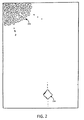
図1は、ハプティックデバイスの下位レベル内の制御電極の通常の配置を示す。この配置は、当該技術分野において既知であり、2つの電極軸からなる。電極102は、第1の軸に沿って配向され、第1の信号線106を介して接続され、電極104は、第2の、通常、直交する軸に沿って配向され、第2の信号線108によって接続される。(電極のいかなる上層も存在しない)この配置は、タッチ位置を検知するために多くの場合に使用される。
FIG. 1 shows a typical arrangement of control electrodes in the lower level of the haptic device. This arrangement is known in the art and consists of two electrode axes. The
タッチデバイス内の位置は、2つの手法、自己キャパシタンス及び相互キャパシタンスを用いて検出される。自己キャパシタンス手法は、個々のラインの電圧を所与の量だけ変更するために必要とされる電流又は電荷の一連の測定からなる。電極付近に指が置かれる場合、指は電流又は電荷測定値を変更し、信号を与える。両方の軸上のこれらの信号を調べることによって、タッチ位置を推測することができる。相互キャパシタンス手法は、送信側として取り扱われる一方の電極軸と、受信側として取り扱われる第2の電極軸とを必要とする。送信電極に電圧を印加することができ、結果として生成される信号、通常、電荷又は電流を各受信側電極において測定することができる。指が第1の軸上の或る電極と第2の軸上の別の電極とが交差する場所付近に置かれる場合には、指は受信側電極上の信号を変更することになる。重要なことに、電極の上層の存在が、その実施態様の細部を変更する場合があるが、いずれの検知方策も本発明とともに使用することができる。 Location within the touch device is detected using two approaches, self capacitance and mutual capacitance. The self-capacitance approach consists of a series of measurements of the current or charge required to change the voltage of an individual line by a given amount. When a finger is placed near the electrodes, the finger alters the current or charge measurement and gives a signal. By examining these signals on both axes, the touch location can be inferred. The mutual capacitance approach requires one electrode axis to be treated as the transmitter and a second electrode axis to be treated as the receiver. A voltage can be applied to the transmitting electrodes and the resulting signal, usually charge or current, can be measured at each receiving electrode. If the finger is placed near where one electrode on the first axis intersects another electrode on the second axis, the finger will alter the signal on the receiving electrode. Importantly, the presence of the top layer of the electrode may alter the details of the embodiment, but any sensing strategy can be used with the present invention.
制御電極102及び104を更に用いて、ハプティック信号を導入することができる。例えば、1つの制御電極に印加される電圧が、容量性結合を介して、上層内の浮遊電極のそれぞれの電位を変更することになる。この電位の変化は、人の指に対する電位差を引き起こすことがあり、結果として、上記のような摩擦の変化が生じる。(接地又はタッチデバイスの局所的なグラウンドのような何らかのグラウンドに対する)単一の制御電圧の使用は、「単極」動作と呼ばれる。また、ハプティック効果は双極にすることもでき、その場合、ハプティック効果は、別々の制御電極102及び104上で(接地又はタッチデバイスの局所的なグラウンドのような何らかのグラウンドに対する)正の電圧及び負の電圧を同時に使用することによって引き起こされる。例えば、信号線106を介して第1の軸上の制御電極102に正の電圧を印加することができ、信号線108を介して第2の軸上の制御電極104に負の電圧を印加することができる。上層がない場合、両方の電極102及び104の上方にあり、両方の電極が交差する場所に近い、タッチ面上に置かれた指が、指又は体の電位にかかわらず、ハプティック効果を受けることになる。しかしながら、この効果の強さは、中間層の厚さによって決まり、中間層が厚くなるほど減少する。この同じ方策が本発明でも(より厚い中間層の場合にも)実施される場合があるが、上層上の浮遊電極が互いに異なる電位を採用できるように、下層から上層への容量性結合が構成されるのを確実にすることが重要である。以下において、適切な電極構成を教示する。
一実施形態において、浮遊電極の構成は、制御電極の構成(例えば、図1に示される)と同一である。唯一の違いは、浮遊電極を制御電子回路に接続する信号線106、108が存在しなくなることである。言い換えると、浮遊電極は、互いに電気連通していなくてもよい。さらに、各浮遊電極が対応する制御電極の真上に存在するように2つの層を位置合わせすることができる。この「鏡像」配置は、制御電極に印加される信号が主に浮遊電極に伝えられるように、各制御電極からその対応する浮遊電極への強い容量性結合を確立する。この手法の利点は、浮遊電極を制御電極の延長部分と考えることができ、検知及びハプティックスの両方に関する(並びに検知及びハプティックスを同時に行うための)既知の技法を、変更することなく使用できることである。別の実施形態において、浮遊電極の構成は、制御電極の構成とは異なる。
In one embodiment, the configuration of the floating electrode is identical to the configuration of the control electrode (eg, as shown in FIG. 1). The only difference is that the
「鏡像」手法の不利な点は、一方の軸を他方の軸の上方で交差させる必要があることに起因して、浮遊電極を導電性材料の単層から製造できないことである。近接した2つのサブ層、又は導電性ブリッジ等の既知の技法を使用できるが、これらはコスト及び複雑性を増加させる。さらに、ブリッジ等の或る特定の技法は、前面に実装するには脆弱すぎる場合がある。これらの理由から、ブリッジを用いることなく、導電性材料の単層から浮遊電極を形成することが好ましい。 A disadvantage of the "mirror image" approach is that the floating electrode can not be manufactured from a single layer of conductive material due to the need to cross one axis above the other. While known techniques such as two sublayers in close proximity or conductive bridges can be used, they add cost and complexity. Furthermore, certain techniques such as bridges may be too fragile to be implemented on the front. For these reasons, it is preferable to form the floating electrode from a single layer of conductive material without the use of a bridge.
図2は、単層の浮遊電極の組の一実施形態を示す。ここで、浮遊電極202は実質的に任意の形状を有することができるが、制御電極204のピッチよりかなり小さい。例えば、制御電極204のピッチが5mmである場合には、浮遊電極202はそれぞれ、差し渡しで約0.5mmとすることができる。浮遊電極202の小さいサイズは、浮遊電極が、その表面にわたって横方向に、検知を妨げるほど大量に電荷を搬送しないことを意味する。それでも、浮遊電極202の幅が、指先の皮膚上の凹凸間の特性距離より大きい限り、皮膚と表面とが最も密着している位置まで横方向に電荷が搬送されることになる。これらの位置において、浮遊電極202が全く存在しない状況と比べて、強い垂直抗力が生成されることになる。このようにして、非常に小さい浮遊電極202であっても、ハプティック効果の強さを増すという利点を有することになる。
FIG. 2 illustrates one embodiment of a single layer floating electrode set. Here, the floating
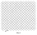
小さい浮遊電極202は何らかの利点を提供するが、サイズが大きくなると、下層上の制御電極への容量性結合が増すので、浮遊電極が大きいほど、より大きな利点が生じる。図3は、各電極303のサイズを大きくした、単層の浮遊電極303の組の別の実施形態を示す。ここで、各浮遊電極302は、下層の制御電極102又は104のダイヤモンド形と位置合わせされる、単一のダイヤモンド形パッチである。この実施形態は、単純である、製造コストが低い、及び丈夫であるという利点を有する。上記の実施形態の場合と同様に、これらの浮遊電極302は、検知方策を妨げない。さらに、浮遊電極302が大きいほど、下層に対してより強い容量性結合を与える。制御電極102又は104から各浮遊電極302への接続の強さは重なる面積によって決まることに留意されたい。この実施形態において、重なる面積は単一のダイヤモンドのサイズである。これは、先行する実施形態において見られる面積よりずっと大きいが、それでも、「鏡像」手法の場合のような、ダイヤモンドの行又は列全体に関連付けられる重なる面積よりずっと小さい。
Smaller floating
重なる面積を更に大きくする1つの方法は、浮遊電極302のためにより大きいダイヤモンド形を利用することである。例えば、ダイヤモンドの幅を2倍にし、4倍の面積を与えることができる。この場合、浮遊するダイヤモンドは、第1の軸上の1つの制御電極102と第2の軸上の1つの制御電極104とが交差する場所に位置合わせされることになる。強いハプティック信号を生成するために、2つの制御電極102及び104のそれぞれに同じ電圧が印加されることになる。しかしながら、この手法の場合に難しいことは、指が、2つ以上のそのような大きいダイヤモンド電極の上方に存在するほど大きくない場合があることである。上記のように、指は、異なる電位を有する少なくとも2つの電極の上方に存在することが好ましい。
One way to further increase the overlapping area is to utilize a larger diamond shape for the floating
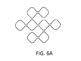
それゆえ、代替の実施形態は、図4〜図7に示されるように「タイル張りされた」パッチからなる。ここで、各浮遊電極は、2つ以上のダイヤモンドの相互接続によって形成されるタイルであり、ダイヤモンドは、下層の制御電極のダイヤモンド形と位置合わせされる。さらに、所与のタイル上の全てのダイヤモンドが、単一の電極軸上の下層のダイヤモンドと位置合わせされる。このようにして、図1に示されるような、下層電極の「格子縞」パターンが、それらのタイルにおいても見られる。タイルは、一群の異なるサイズにおいて作製される場合がある。 Thus, an alternative embodiment consists of "tiled" patches as shown in FIGS. 4-7. Here, each floating electrode is a tile formed by the interconnection of two or more diamonds, the diamonds being aligned with the diamond shape of the underlying control electrode. Furthermore, all the diamonds on a given tile are aligned with the underlying diamond on a single electrode axis. In this way, a "grid" pattern of lower layer electrodes, as shown in FIG. 1, is also seen in those tiles. The tiles may be made in a group of different sizes.
この浮遊電極群内の最も小さいタイルはそれぞれ、図4Aに示されるように、「ダンベル」形に接続される2つのダイヤモンドからなる。2つのダイヤモンド402及び404はトレース406を介して接続され、実質的に「ダンベル」形を形成する。各ダンベルは、個々の制御電極102又は104上の2つのダイヤモンドと位置合わせされる場合があるか、又は2つの隣接する制御電極102又は104上の2つのダイヤモンドと位置合わせされる場合がある。いずれの場合も、下層のダイヤモンドは、可能な限り最も強いハプティック効果を生み出すために、実質的に同じ電圧に制御されるべきである。さらに、2つの異なる軸上の制御電極102及び104と位置合わせされるダンベルは、異なる電位に導かれる場合がある。
The smallest tiles in this floating electrode group each consist of two diamonds connected in a "dumbbell" shape, as shown in FIG. 4A. Two
図4Bは、第1の組のダンベル408が、第2の組のダンベル410と逆の電荷を有するダンベルの配置を示す。例示として、第1の組のダンベル408は正の電荷を有することができ、一方、第2の組のダンベル410は負の電荷を有することができる。隣接する組の第1の組のダンベル408は、第2の組のダンベル410内の電極を接合するトレース406によって分離される。
FIG. 4B shows the placement of dumbbells where the first set of
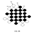
図5Aは、同じ群内により大きいタイルを有するグループ浮遊電極502の一実施形態を示す。ここで、タイルは3×3の格子縞パターンの対角線上に存在するダイヤモンドからなる。これらのタイルで平面をタイル張りすることが依然として可能であり、各タイルを単一の軸上の下層の電極と位置合わせすることが依然として可能であることに留意されたい。この、より大きいタイルパターンは、下層の電極と重なる面積がより大きいという利点を有する。この実施形態でも同様に、中央の電極504が、トレース508を介して、少なくとも4つの放射状電極506に接続される。一実施形態において、各放射状電極506間の角度は実質的に同じである。別の実施形態において、各放射状電極506間の角度は、放射状電極506ごとに異なる。
FIG. 5A shows an embodiment of a
一実施形態において、制御電極102及び104並びに浮遊電極502は実質的に同じサイズ及び形状を有する。別の実施形態において、制御電極102及び104並びに浮遊電極502は異なるサイズ及び形状を有する。別の実施形態において、上層は1つの浮遊電極を含む。別の実施形態において、上層は複数の浮遊電極を含む。
In one embodiment,
図5Bは、浮遊電極502のグループの配置の一実施形態を示す。浮遊電極502の各グループは、浮遊電極502の隣接するグループとは異なる電荷を有する。浮遊電極502の隣接するグループ上の更なる放射状電極506はトレース508によって分離される。一実施形態において、浮遊電極502によって生成されるハプティック信号は単極である。別の実施形態において、浮遊電極によって生成されるハプティック信号は双極である。
FIG. 5B shows an embodiment of an arrangement of groups of floating
図6及び図7はそれぞれ、4×4及び5×5の格子縞からもたらされる、この群内の次に大きい2つのタイルパターンを示す。同じ基本的な「分岐スポーク(branched spoke)」パターンに従って、更に大きいパターンも可能である。パターンが大きいほど、下層の制御電極からの容量性結合が増すという利点があるが、検知がより難しくなる場合がある。すなわち、浮遊電極のサイズに起因して、それらの電極は、指を制御電極の組全体により強く結合することになり、位置情報を確定しにくくなる。 Figures 6 and 7 show the next two largest tile patterns in this group, resulting from 4x4 and 5x5 plaids, respectively. Larger patterns are also possible, according to the same basic "branched spoke" pattern. Larger patterns have the advantage of increasing capacitive coupling from the underlying control electrode, but may be more difficult to detect. That is, due to the size of the floating electrodes, they will bind the finger more strongly to the entire set of control electrodes, making it difficult to determine position information.
図8及び図9は、大きい浮遊電極の利点と、高分解能センシングの必要性とを組み合わせた電極配置の別の実施形態を示す。この手法はダイヤモンド形を完全になくし、代わりに、忠実に複製されたタイルを使用し、それにより、両方の層上のタイルが同じ形状を有し、位置合わせされる。さらに、電極は下層から上層への強い容量性結合を与えるほどのサイズを有し、タイルは、タッチ面を覆うために必要とされる全数が相応である(例えば、x電極及びy電極を使用する従来のパターンによって使用される全電極数に相当する)ほど十分に大きく、タイルはそれぞれ、指がいつも複数の電極と接触しており、測定された信号から唯一の指位置をいつも計算できるような方法でかみ合わされる。 Figures 8 and 9 illustrate another embodiment of an electrode arrangement that combines the advantages of large floating electrodes with the need for high resolution sensing. This approach completely eliminates the diamond shape and instead uses faithfully replicated tiles so that the tiles on both layers have the same shape and are aligned. Furthermore, the electrodes have a size sufficient to provide strong capacitive coupling from the lower layer to the upper layer, and the tiles are commensurate with the total number required to cover the touch surface (e.g. using x and y electrodes) Large enough to correspond to the total number of electrodes used by the conventional pattern, and each tile has its finger always in contact with multiple electrodes so that only one finger position can always be calculated from the measured signal Meshed in a variety of ways.
図8は、制御電極及び浮遊電極のために使用することができる電極形状の例示である。各電極800は、第1の電極802及び第2の電極804からなるパターンを含む。第1の電極802は実質的に星形であり、第2の電極804は、星形と絡み合う形状を有する。一実施形態において、第2の電極は、「フロレット(florets)」のような形状を有する。一実施形態において、第2の電極804は大きく、互いにかみ合う分岐した形状である。とりわけ、フロレットの空間的な広がりは、その間隔よりずっと大きい。例えば、図8に示されるように、水平軸に沿った第2の電極804の幅は、第2の電極804の水平方向のピッチのほぼ2倍の大きさである。別の実施形態において、第2の電極804の水平方向及び垂直方向のピッチは20mmとすることができ、単一の第2の電極804によって覆われる面積は約380mm2とすることができる。逆に、図1に示されるような、ダイヤモンドパターンは、5mmの対角線を有することができ、各ダイヤモンドは12.5mm2の面積を有することができる。したがって、1つの第2の電極804は約30個のダイヤモンドと同じ面積を有するか、又は1つの電極の長さが150mmである。第1の電極802は第2の電極804よりずっと小さく、かみ合うのではなく、正確なタッチ位置を計算するために使用することができる付加信号を与える。一実施形態において、最下層上の各第2の電極804は個々に制御されるが、第1の電極802はグループ単位で制御される場合がある。例えば、1つの可能性は第1の電極802の4つのグループを有することである。各水平行に沿って、交互の第1の電極802が同じグループ内で制御されることになり、各垂直列に沿って、交互の第2の電極が同じグループ内で制御されることになる。第1の電極802をグループ化することによって、第1の電極802を制御するために必要とされる制御チャネルの数が削減される。通常動作中に、第1の電極802が指又は他の付属物によって係合されるとき、第1の電極802からの信号と、1つ以上の第2の電極804からの信号との組み合わせを用いて、タッチの正確な位置が特定されることになる。
FIG. 8 is an illustration of electrode shapes that can be used for control and floating electrodes. Each
最上面上のどこに一本の指が置かれようとも、この指は、いくつかの第2の電極804と、同様に、おそらく1つの第1の電極802とに極めて近接することになる。重要なことに、取り得る各指位置からの信号は一意的であり、電極から得られた信号に基づいて指位置を計算できるようにする。信号からタッチ座標が抽出される、この「逆」計算を実行する複数の方法がある。例えば、1つの手法は、タッチ位置ごとの信号の組を記憶し、その後、これらの記憶された信号を、タッチ座標を返すルックアップテーブルとして使用することである。タッチ位置ごとの勾配の組を記憶することが更に有利である。勾配情報は、位置特有のヤコビ行列として表すことができる。

指位置に基づいて、ハプティックスを駆動するための電極を選択することができる。例示として、上記のように、制御電極を用いて、タッチ面と付属物とが係合する位置を特定することができ、制御電極から分離された層上にあり、制御電極と相互に導電作用する浮遊電極が、上記で論じられたように、ハプティック機能を果たすことができる。一般的に言うと、指の真下にある面積の約半分を一方の極性に帯電させ、その面積の約半分を逆の極性に帯電させることが好ましい。また、同じ極性の電極間の相互キャパシタンスが信号強度を強めるように、それらの電極をグループ化することも好ましい。 Based on the finger position, an electrode can be selected to drive the haptics. By way of illustration, as described above, the control electrode can be used to identify the position where the touch surface and the appendage engage, on a layer separated from the control electrode, and conductive to the control electrode. Floating electrodes can perform a haptic function, as discussed above. Generally speaking, it is preferable to charge about half of the area directly under the finger to one polarity and to charge about half of the area to the opposite polarity. It is also preferable to group the electrodes so that the mutual capacitance between the electrodes of the same polarity enhances the signal strength.
種々の電極への電気的接続は、図9及び図10に示されるように行うことができる。最初に図10を参照すると、タッチパネルが最下層1002と、絶縁層1004と、相互接続層1006と、中間層1008と、上層1010と、カバー層1012とを含む。最下層1002は、当該技術分野において既知であるいくつかの材料及びプロセスのいずれかを用いて、絶縁層1004でコーティングすることができる。例えば、絶縁層1004は透明ポリマーから形成することができる。絶縁層1004は、最下層上の各電極に近づくことができる開口部を残すために、スクリーン印刷することができるか、フォトリソグラフィによりエッチングすることができるか、又は別の方法でパターニングすることができる。相互接続層1006は、絶縁層1004の表面に塗布し、その後、各電極への電気的接続を形成するようにパターニングすることができる。代替的には、裸眼では容易に視認できない銀ナノワイヤ又は他の導体を用いて、電気的接続を形成することができる。パッシベーション、相互接続の保護、屈折率整合、及び電気的雑音からの隔離(図示せず)のための付加層を塗布することもできる。
Electrical connections to the various electrodes can be made as shown in FIGS. Referring first to FIG. 10, the touch panel includes a
図9は、相互接続層1006上の電気的接続のパターンの一実施形態を示す。第1の接続線902が、1つの行内の交互の第1の電極802を接続し、第2の接続線904が、第1の接続線902に接続されない第1の電極802を接続する。各接続線902及び904は透明導体から形成される。更なる接続線906、908、910及び912がそれぞれ、1つの第2の電極804に接続する。さらに、これらの導体間には広い間隙ではなく、通常、細い消去線(deletion line)が存在する。好ましい実施形態において、消去線は、幅100ミクロンであるが、それより細い線又は太い線が使用される場合もある。また、消去線は、視覚的に検出するのをより難しくするために、示すように完全に真っすぐではなく、幾分不規則な形状とすることもできる。図9内の半円形又は円形エリアは、相互接続電極が絶縁層を通り抜け、最下層の電極との接続を行う位置を示す。
FIG. 9 illustrates one embodiment of a pattern of electrical connections on
図9に示されるように、所望により、全ての電気的接続を一方のエッジに持って行くことができる。代替的には、電気的接続は複数のエッジに沿って行うことができる。また、図9は、4つのグループに分けられる、第1の電極802のグループ化を示す。各グループにはバスバー914、916、918又は920が関連付けられ、それは最下層の一部とすることができる。他の実施形態では、限定はしないが、フレックスケーブル、又は制御盤上若しくはチップ上、等の他の方法を用いてグループ化するために、必要に応じて第1の電極802の相互接続が実行される。
All electrical connections can be brought to one edge if desired, as shown in FIG. Alternatively, electrical connections can be made along multiple edges. FIG. 9 also shows the grouping of the
上層の浮遊電極を形成するために、数多くの他のパターンも使用することができる。例えば、第1の電極802をなくし、第2の電極804のみを使用することができる。第2の電極804のフロレットは、表面をタイル張りする実質的に任意の形状をとることができる。重要なのは、それらの電極が、必要なハプティック信号及び検知信号を生成するほど十分に下層電極に容量性結合することだけである。
Many other patterns can also be used to form the overlying floating electrode. For example, the
本明細書において提示される浮遊上層1010及び被制御下層1012アーキテクチャの重要な利点は、かき傷等の、タッチスクリーンへの典型的な形態の損傷に耐性があることである。これは、第一には、相対的に厚い中間透明層1008によって下層電極1002が保護されるためであり、第二には、上層電極1010が、制御電子回路との導電結合ではなく、下層電極1002との容量性結合を介して信号を得るためである。導電結合が、電極を横断するかき傷によって損なわれるのに対して、容量性結合は損なわれない。本発明の場合、上層電極1010の損傷の結果として、何らかの性能(例えば、ハプティック効果の強さ)の損失が生じる場合があるが、タッチ検知又はハプティック出力が全く機能しなくなることはないはずである。かき傷からの保護に加えて、本発明は同様に、擦り傷、水分、化学薬品、静電放電、更にはカバーレンズの完全な破損(下層がカバーレンズとは別の構成要素である場合)等の他の形態の損傷からの保護も与える。
An important advantage of the floating
図11は、ハプティックデバイスを製造するために使用されるプロセスの概略図を示す。ステップ1102において、中間層1008の最上面が上層の電極層1010でコーティングされる。ステップ1104において、上層1010から浮遊電極がパターニングされる。浮遊電極は、単一の部品、マルチアップ(multi-up)(マザーシート)、又はハイブリッドプロセス(最初にシートの形で開始し、プロセスの或る段階において個々のセンサーに切り分け、単一の部品として処理し続ける)において処理することができる。浮遊電極は、本明細書において説明される方法のいずれかを用いて形成することができる。ステップ1106において、最上層1010内の浮遊電極の上方にカバー層1012が塗布される。カバー層1012は、疎油性、サファイア様ガラス、屈折率整合、抗菌コーティング及び当該技術分野において既知である他のコーティング等の膜を含むことができる。ステップ1108において、中間層1008の反対側に標準的なP−capセンサー(図1に示される)が形成される(代替的には、ガラスの反対側に標準的なP−capセンサーを張り付けることができる;また、代替的には、或る特定の実施形態の場合に、最下層上に鏡像電極を形成することができる)。
FIG. 11 shows a schematic of the process used to manufacture the haptic device. In
ガラス上にP−capセンサー層が存在する前に硬質のオーバーコートが加工されるので、オーバーコートの堆積又は焼き鈍しにおいてより高い加工温度を使用することができ、結果として、性能がより良好になり、材料の選択の幅が広がる。 Because the hard overcoat is processed before the P-cap sensor layer is present on the glass, higher processing temperatures can be used in overcoat deposition or annealing, resulting in better performance. , The range of choice of materials broadens.
P−capセンサーを張り付け、ハプティック電極を含むカバーシートを使用することが、本発明を実施する別の方法である。既存のP−capセンサーにカバーシート/レンズを追加することが、コスト効率を高め、既に当該分野にあるセンサーにハプティックを追加するのを容易にする。この場合、ハプティック信号を高める特別な回路が、電子回路に追加される必要がある。代替的には、標準的なP−capタッチスクリーンから開始して、反対(タッチ)面をハプティック電極及び任意選択のオーバーコートでコーティングすることができる。 Applying a P-cap sensor and using a cover sheet containing haptic electrodes is another way of practicing the invention. Adding cover sheets / lenses to existing P-cap sensors is more cost effective and facilitates the addition of haptics to sensors already in the field. In this case, special circuitry to enhance the haptic signal needs to be added to the electronic circuitry. Alternatively, starting with a standard P-cap touch screen, the opposite (touch) side can be coated with a haptic electrode and an optional overcoat.
中間層厚は、5ミクロン〜6mmに及ぶことがあるが、好ましい厚さは100ミクロン〜500ミクロンである。その厚さは、必要とされる機械的強度、処理機能、要求されるハプティック信号強度、最大印加電圧、光学特性等によって決まる。 The intermediate layer thickness may range from 5 microns to 6 mm, but the preferred thickness is 100 microns to 500 microns. The thickness is determined by the required mechanical strength, processing capability, required haptic signal strength, maximum applied voltage, optical properties, etc.
当業者であれば認識するように、本開示は、種々の静電デバイス上で、駆動電圧を下げても、同じ所望のハプティック効果を維持するように実施することができる。そのようなデバイスの例は静電チャック、電気吸着を利用するデバイス(ロボット、マテリアルハンドリング等)である。一実施形態において、タッチ面は硬質面である。別の実施形態において、タッチ面は、平面、曲面、湾曲、モーフィング又は他の可撓性表面を含む、可撓性表面である。さらに、ハプティック電極がハプティック信号に直接接続される必要がないので、底部電極と最も外側にある電極との間の極めて大きい分離を達成するために、電極/非導電性基板を何度も積重することができる。 As those skilled in the art will appreciate, the present disclosure can be implemented on various electrostatic devices to lower the drive voltage while maintaining the same desired haptic effect. Examples of such devices are electrostatic chucks, devices that use electrical adsorption (robots, material handling, etc.). In one embodiment, the touch surface is a hard surface. In another embodiment, the touch surface is a flexible surface, including planar, curved, curved, morphing or other flexible surfaces. Furthermore, because the haptic electrode does not have to be connected directly to the haptic signal, the electrode / non-conductive substrate can be stacked many times to achieve a very large separation between the bottom electrode and the outermost electrode. can do.
本開示では、数量を特定しない語は、単数のもの及び複数のものの両方を含むように解釈されるべきである。逆に、複数の要素に対するいかなる言及も、適切である場合は、単数のものを含むものとする。 In the present disclosure, terms which do not specify a quantity should be construed to include both singular and plural. Conversely, any reference to more than one element is intended to include the singular as appropriate.
本明細書に開示される、本発明における好ましい実施形態に対する様々な変更及び修正は、当業者には明らかであろうと理解されるべきである。そのような変更及び修正は、本開示の趣旨及び範囲から逸脱することなく、かつその意図された利点を損なうことなく行われ得る。したがって、そのような変更及び修正は、添付の特許請求の範囲に含まれるものと意図される。
It should be understood that various changes and modifications to the preferred embodiments of the invention disclosed herein will be apparent to those skilled in the art. Such changes and modifications can be made without departing from the spirit and scope of the present disclosure and without diminishing its intended advantages. Accordingly, such changes and modifications are intended to be included within the scope of the appended claims.
Claims (20)
複数の制御電極を含む下層と、
複数のハプティック電極を含む上層と、
前記下層と前記上層との間にある中間層と、
を含み、
前記ハプティック電極は制御電極に導電接続されない、ハプティックタッチスクリーン。 A haptic touch screen,
A lower layer comprising a plurality of control electrodes,
An upper layer comprising a plurality of haptic electrodes,
An intermediate layer between the lower layer and the upper layer,
Including
The haptic touch screen, wherein the haptic electrode is not conductively connected to the control electrode.
複数のハプティック電極を含む上層を形成することと、
複数の制御電極を含む下層を形成することと、
前記下層と前記上層との間に中間層を形成することと、
を含み、
前記ハプティック電極は制御電極に導電接続されない、方法。 A method of making a haptic touch screen comprising
Forming an upper layer including a plurality of haptic electrodes;
Forming a lower layer including a plurality of control electrodes;
Forming an intermediate layer between the lower layer and the upper layer;
Including
The method wherein the haptic electrode is not conductively connected to the control electrode.
The method according to claim 11, wherein the haptic electrodes are grouped and each group of haptic electrodes has a different charge.
Applications Claiming Priority (5)
| Application Number | Priority Date | Filing Date | Title |
|---|---|---|---|
| US201662342594P | 2016-05-27 | 2016-05-27 | |
| US62/342,594 | 2016-05-27 | ||
| US15/606,440 US10423228B2 (en) | 2016-05-27 | 2017-05-26 | Haptic touch screen and method of operating the same |
| US15/606,440 | 2017-05-26 | ||
| PCT/US2017/034750 WO2017205785A1 (en) | 2016-05-27 | 2017-05-26 | Haptic touch screen and method of operating the same |
Publications (2)
| Publication Number | Publication Date |
|---|---|
| JP2019521423A true JP2019521423A (en) | 2019-07-25 |
| JP2019521423A5 JP2019521423A5 (en) | 2021-11-18 |
Family
ID=60412678
Family Applications (1)
| Application Number | Title | Priority Date | Filing Date |
|---|---|---|---|
| JP2018562020A Pending JP2019521423A (en) | 2016-05-27 | 2017-05-26 | Haptic touch screen and method of operating it |
Country Status (4)
| Country | Link |
|---|---|
| US (1) | US10423228B2 (en) |
| JP (1) | JP2019521423A (en) |
| KR (2) | KR102443039B1 (en) |
| WO (1) | WO2017205785A1 (en) |
Families Citing this family (12)
| Publication number | Priority date | Publication date | Assignee | Title |
|---|---|---|---|---|
| KR102496554B1 (en) * | 2016-05-25 | 2023-02-08 | 삼성디스플레이 주식회사 | Touch screen panel |
| JP7011141B2 (en) * | 2016-06-24 | 2022-02-10 | 天馬微電子有限公司 | Tactile presentation panels, tactile presentation devices and electronic devices |
| US10775890B2 (en) | 2017-09-27 | 2020-09-15 | Apple Inc. | Electronic device having a piezoelectric body for friction haptics |
| US10585482B2 (en) | 2017-09-27 | 2020-03-10 | Apple Inc. | Electronic device having a hybrid conductive coating for electrostatic haptics |
| US10248211B1 (en) | 2017-09-28 | 2019-04-02 | Apple Inc. | Ground-shifted touch input sensor for capacitively driving an electrostatic plate |
| JP7199194B2 (en) * | 2017-12-28 | 2023-01-05 | Tianma Japan株式会社 | Touch panel and touch panel device |
| US11016568B2 (en) | 2018-07-24 | 2021-05-25 | The Nielsen Company (Us), Llc | Methods and apparatus to monitor haptic vibrations of touchscreens |
| US11520406B2 (en) | 2019-05-28 | 2022-12-06 | Tanvas, Inc. | Bipolar projected haptics with balanced loading |
| US11337034B1 (en) | 2020-08-13 | 2022-05-17 | Rockwell Collins, Inc. | Staggered examination of non-trusted receiver information |
| US11455039B2 (en) | 2020-09-17 | 2022-09-27 | Rockwell Collins, Inc. | Advanced haptics in touchscreen avionics lower level device simulators |
| US11442547B1 (en) | 2021-05-10 | 2022-09-13 | Rockwell Collins, Inc. | Software defined hard keys leveraging flexible display hardware to achieve haptic display solution |
| US11921927B1 (en) * | 2021-10-14 | 2024-03-05 | Rockwell Collins, Inc. | Dynamic and context aware cabin touch-screen control module |
Citations (6)
| Publication number | Priority date | Publication date | Assignee | Title |
|---|---|---|---|---|
| JP2013058154A (en) * | 2011-09-09 | 2013-03-28 | Alps Electric Co Ltd | Tactile stimulation generation device |
| US20130307789A1 (en) * | 2012-05-17 | 2013-11-21 | Sharp Kabushiki Kaisha | Touch-screen device including tactile feedback actuator |
| US20130313098A1 (en) * | 2012-05-25 | 2013-11-28 | Chunghwa Picture Tubes, Ltd. | Electrode array of touch panel |
| KR20140145707A (en) * | 2013-06-14 | 2014-12-24 | 엘지디스플레이 주식회사 | Haptic touch screen |
| WO2015127270A2 (en) * | 2014-02-21 | 2015-08-27 | Northwestern University | Haptic display with simultaneous sensing and actuation |
| JP2016001470A (en) * | 2014-06-05 | 2016-01-07 | イマージョン コーポレーションImmersion Corporation | Systems and methods for induced electrostatic haptic effects |
Family Cites Families (11)
| Publication number | Priority date | Publication date | Assignee | Title |
|---|---|---|---|---|
| ATE320059T1 (en) * | 2001-12-12 | 2006-03-15 | Koninkl Philips Electronics Nv | DISPLAY SYSTEM WITH TACTILE GUIDANCE |
| US7567681B2 (en) * | 2003-09-03 | 2009-07-28 | Sri International | Surface deformation electroactive polymer transducers |
| HK1122460A2 (en) | 2005-03-04 | 2009-05-15 | Apple Inc | Multi-functional hand-held device |
| US9829977B2 (en) * | 2008-04-02 | 2017-11-28 | Immersion Corporation | Method and apparatus for providing multi-point haptic feedback texture systems |
| EP2239793A1 (en) * | 2009-04-11 | 2010-10-13 | Bayer MaterialScience AG | Electrically switchable polymer film structure and use thereof |
| US9618739B2 (en) * | 2010-09-09 | 2017-04-11 | Philips Lighting Holding B.V. | Electoactive polymer actuator |
| US10013058B2 (en) * | 2010-09-21 | 2018-07-03 | Apple Inc. | Touch-based user interface with haptic feedback |
| US9122325B2 (en) * | 2011-05-10 | 2015-09-01 | Northwestern University | Touch interface device and method for applying controllable shear forces to a human appendage |
| US9195350B2 (en) | 2011-10-26 | 2015-11-24 | Nokia Technologies Oy | Apparatus and associated methods |
| KR102161723B1 (en) * | 2013-05-07 | 2020-10-06 | 삼성디스플레이 주식회사 | Haptic panel, display apparatus having the same |
| US20160124548A1 (en) * | 2014-11-03 | 2016-05-05 | Northwestern University | Materials and structures for haptic displays with simultaneous sensing and actuation |
-
2017
- 2017-05-26 JP JP2018562020A patent/JP2019521423A/en active Pending
- 2017-05-26 KR KR1020187034239A patent/KR102443039B1/en active IP Right Grant
- 2017-05-26 US US15/606,440 patent/US10423228B2/en active Active
- 2017-05-26 WO PCT/US2017/034750 patent/WO2017205785A1/en unknown
- 2017-05-26 KR KR1020227019273A patent/KR20220084186A/en not_active Application Discontinuation
Patent Citations (7)
| Publication number | Priority date | Publication date | Assignee | Title |
|---|---|---|---|---|
| JP2013058154A (en) * | 2011-09-09 | 2013-03-28 | Alps Electric Co Ltd | Tactile stimulation generation device |
| US20130307789A1 (en) * | 2012-05-17 | 2013-11-21 | Sharp Kabushiki Kaisha | Touch-screen device including tactile feedback actuator |
| US20130313098A1 (en) * | 2012-05-25 | 2013-11-28 | Chunghwa Picture Tubes, Ltd. | Electrode array of touch panel |
| KR20140145707A (en) * | 2013-06-14 | 2014-12-24 | 엘지디스플레이 주식회사 | Haptic touch screen |
| WO2015127270A2 (en) * | 2014-02-21 | 2015-08-27 | Northwestern University | Haptic display with simultaneous sensing and actuation |
| JP2017506395A (en) * | 2014-02-21 | 2017-03-02 | タンヴァス, インコーポレイテッドTanvas, Inc. | Tactile display with simultaneous detection and actuation |
| JP2016001470A (en) * | 2014-06-05 | 2016-01-07 | イマージョン コーポレーションImmersion Corporation | Systems and methods for induced electrostatic haptic effects |
Also Published As
| Publication number | Publication date |
|---|---|
| KR102443039B1 (en) | 2022-09-13 |
| KR20190017758A (en) | 2019-02-20 |
| US10423228B2 (en) | 2019-09-24 |
| WO2017205785A1 (en) | 2017-11-30 |
| KR20220084186A (en) | 2022-06-21 |
| US20170344119A1 (en) | 2017-11-30 |
Similar Documents
| Publication | Publication Date | Title |
|---|---|---|
| JP2019521423A (en) | Haptic touch screen and method of operating it | |
| JP5753084B2 (en) | Manufacturing method of composite electrode | |
| US10048820B2 (en) | Touch panel and manufacturing method thereof | |
| TW201706803A (en) | Touch 3D-signal input equipment and multi-function touch panel | |
| US11886641B2 (en) | Method and apparatus for finger position tracking and haptic display using conductive islands | |
| WO2019030987A1 (en) | Tactile sensation presentation panel, tactile sensation presentation touch panel, and tactile sensation presentation touch display | |
| JP2020027661A (en) | Touch-fingerprint complex sensor and electronic apparatus including the same | |
| WO2019021835A1 (en) | Touch panel conductive member and touch panel | |
| EP3336670B1 (en) | Touch sensor and display device including the same | |
| CN109416582B (en) | Tactile touch screen and operation method thereof | |
| TWM584918U (en) | Touch panel capable of reducing parasitic capacitance | |
| KR101366358B1 (en) | Touch screen and method for manufacturing them | |
| CN108845698A (en) | Touch-control structure, touch control method and touch device | |
| JP7199194B2 (en) | Touch panel and touch panel device |
Legal Events
| Date | Code | Title | Description |
|---|---|---|---|
| A621 | Written request for application examination |
Free format text: JAPANESE INTERMEDIATE CODE: A621 Effective date: 20200521 |
|
| A977 | Report on retrieval |
Free format text: JAPANESE INTERMEDIATE CODE: A971007 Effective date: 20210331 |
|
| A131 | Notification of reasons for refusal |
Free format text: JAPANESE INTERMEDIATE CODE: A131 Effective date: 20210406 |
|
| A601 | Written request for extension of time |
Free format text: JAPANESE INTERMEDIATE CODE: A601 Effective date: 20210702 |
|
| A601 | Written request for extension of time |
Free format text: JAPANESE INTERMEDIATE CODE: A601 Effective date: 20210902 |
|
| A524 | Written submission of copy of amendment under article 19 pct |
Free format text: JAPANESE INTERMEDIATE CODE: A524 Effective date: 20211001 |
|
| A521 | Request for written amendment filed |
Free format text: JAPANESE INTERMEDIATE CODE: A523 Effective date: 20211005 |
|
| A131 | Notification of reasons for refusal |
Free format text: JAPANESE INTERMEDIATE CODE: A131 Effective date: 20220315 |
|
| A601 | Written request for extension of time |
Free format text: JAPANESE INTERMEDIATE CODE: A601 Effective date: 20220613 |
|
| A601 | Written request for extension of time |
Free format text: JAPANESE INTERMEDIATE CODE: A601 Effective date: 20220812 |
|
| A521 | Request for written amendment filed |
Free format text: JAPANESE INTERMEDIATE CODE: A523 Effective date: 20220914 |
|
| A02 | Decision of refusal |
Free format text: JAPANESE INTERMEDIATE CODE: A02 Effective date: 20221213 |