JP2011523863A - A substrate layer adapted to carry a sensor, actuator or electrical component - Google Patents
A substrate layer adapted to carry a sensor, actuator or electrical component Download PDFInfo
- Publication number
- JP2011523863A JP2011523863A JP2011510078A JP2011510078A JP2011523863A JP 2011523863 A JP2011523863 A JP 2011523863A JP 2011510078 A JP2011510078 A JP 2011510078A JP 2011510078 A JP2011510078 A JP 2011510078A JP 2011523863 A JP2011523863 A JP 2011523863A
- Authority
- JP
- Japan
- Prior art keywords
- substrate layer
- layer structure
- slits
- sensor
- slit
- Prior art date
- Legal status (The legal status is an assumption and is not a legal conclusion. Google has not performed a legal analysis and makes no representation as to the accuracy of the status listed.)
- Pending
Links
Images


Classifications
-
- G—PHYSICS
- G01—MEASURING; TESTING
- G01K—MEASURING TEMPERATURE; MEASURING QUANTITY OF HEAT; THERMALLY-SENSITIVE ELEMENTS NOT OTHERWISE PROVIDED FOR
- G01K1/00—Details of thermometers not specially adapted for particular types of thermometer
- G01K1/16—Special arrangements for conducting heat from the object to the sensitive element
- G01K1/165—Special arrangements for conducting heat from the object to the sensitive element for application in zero heat flux sensors
-
- A—HUMAN NECESSITIES
- A61—MEDICAL OR VETERINARY SCIENCE; HYGIENE
- A61B—DIAGNOSIS; SURGERY; IDENTIFICATION
- A61B5/00—Measuring for diagnostic purposes; Identification of persons
- A61B5/01—Measuring temperature of body parts ; Diagnostic temperature sensing, e.g. for malignant or inflamed tissue
-
- G—PHYSICS
- G01—MEASURING; TESTING
- G01K—MEASURING TEMPERATURE; MEASURING QUANTITY OF HEAT; THERMALLY-SENSITIVE ELEMENTS NOT OTHERWISE PROVIDED FOR
- G01K13/00—Thermometers specially adapted for specific purposes
- G01K13/20—Clinical contact thermometers for use with humans or animals
-
- A—HUMAN NECESSITIES
- A61—MEDICAL OR VETERINARY SCIENCE; HYGIENE
- A61B—DIAGNOSIS; SURGERY; IDENTIFICATION
- A61B2562/00—Details of sensors; Constructional details of sensor housings or probes; Accessories for sensors
- A61B2562/02—Details of sensors specially adapted for in-vivo measurements
- A61B2562/0271—Thermal or temperature sensors
- A61B2562/0276—Thermal or temperature sensors comprising a thermosensitive compound
-
- A—HUMAN NECESSITIES
- A61—MEDICAL OR VETERINARY SCIENCE; HYGIENE
- A61B—DIAGNOSIS; SURGERY; IDENTIFICATION
- A61B2562/00—Details of sensors; Constructional details of sensor housings or probes; Accessories for sensors
- A61B2562/16—Details of sensor housings or probes; Details of structural supports for sensors
- A61B2562/164—Details of sensor housings or probes; Details of structural supports for sensors the sensor is mounted in or on a conformable substrate or carrier
-
- A—HUMAN NECESSITIES
- A61—MEDICAL OR VETERINARY SCIENCE; HYGIENE
- A61B—DIAGNOSIS; SURGERY; IDENTIFICATION
- A61B5/00—Measuring for diagnostic purposes; Identification of persons
- A61B5/68—Arrangements of detecting, measuring or recording means, e.g. sensors, in relation to patient
-
- Y—GENERAL TAGGING OF NEW TECHNOLOGICAL DEVELOPMENTS; GENERAL TAGGING OF CROSS-SECTIONAL TECHNOLOGIES SPANNING OVER SEVERAL SECTIONS OF THE IPC; TECHNICAL SUBJECTS COVERED BY FORMER USPC CROSS-REFERENCE ART COLLECTIONS [XRACs] AND DIGESTS
- Y10—TECHNICAL SUBJECTS COVERED BY FORMER USPC
- Y10T—TECHNICAL SUBJECTS COVERED BY FORMER US CLASSIFICATION
- Y10T29/00—Metal working
- Y10T29/49—Method of mechanical manufacture
- Y10T29/49002—Electrical device making
- Y10T29/49117—Conductor or circuit manufacturing
- Y10T29/49124—On flat or curved insulated base, e.g., printed circuit, etc.
- Y10T29/4913—Assembling to base an electrical component, e.g., capacitor, etc.
-
- Y—GENERAL TAGGING OF NEW TECHNOLOGICAL DEVELOPMENTS; GENERAL TAGGING OF CROSS-SECTIONAL TECHNOLOGIES SPANNING OVER SEVERAL SECTIONS OF THE IPC; TECHNICAL SUBJECTS COVERED BY FORMER USPC CROSS-REFERENCE ART COLLECTIONS [XRACs] AND DIGESTS
- Y10—TECHNICAL SUBJECTS COVERED BY FORMER USPC
- Y10T—TECHNICAL SUBJECTS COVERED BY FORMER US CLASSIFICATION
- Y10T428/00—Stock material or miscellaneous articles
- Y10T428/24—Structurally defined web or sheet [e.g., overall dimension, etc.]
- Y10T428/24273—Structurally defined web or sheet [e.g., overall dimension, etc.] including aperture
- Y10T428/24298—Noncircular aperture [e.g., slit, diamond, rectangular, etc.]
- Y10T428/24314—Slit or elongated
Landscapes
- Health & Medical Sciences (AREA)
- Life Sciences & Earth Sciences (AREA)
- Physics & Mathematics (AREA)
- General Physics & Mathematics (AREA)
- Engineering & Computer Science (AREA)
- Animal Behavior & Ethology (AREA)
- Biomedical Technology (AREA)
- Heart & Thoracic Surgery (AREA)
- Medical Informatics (AREA)
- Molecular Biology (AREA)
- Surgery (AREA)
- Pathology (AREA)
- General Health & Medical Sciences (AREA)
- Public Health (AREA)
- Veterinary Medicine (AREA)
- Biophysics (AREA)
- Measuring And Recording Apparatus For Diagnosis (AREA)
- Structure Of Printed Boards (AREA)
- Testing Or Calibration Of Command Recording Devices (AREA)
- Measuring Pulse, Heart Rate, Blood Pressure Or Blood Flow (AREA)
Abstract
本発明は、電子機器若しくは部品、又は電気‐機械的若しくは電気‐化学的センサ、又はそれらの組み合わせを担持するように適合された、かつ、人若しくは動物の身体又は生物学的種の表面に取り付けられるように適合された、基板層構造に関する。柔軟な基板層構造の表面は、1つ以上のスリットによって形成される予め固定された形状のパターン構造であるが、この形状は、基板層構造の伸縮性がその下の身体表面の形状に適合するように選択される。 The present invention is adapted to carry electronic devices or components, or electro-mechanical or electro-chemical sensors, or combinations thereof, and attach to the surface of a human or animal body or biological species It relates to a substrate layer structure adapted to The surface of the flexible substrate layer structure is a pattern structure with a pre-fixed shape formed by one or more slits, but this shape matches the shape of the underlying body surface with the elasticity of the substrate layer structure Selected to do.
Description
本発明は、センサ、アクチュエータ、又は電気部品を担持するように適合された、かつ、人若しくは動物の身体又は生物学的種の表面に取り付けられるように適合された、基板層構造に関する。 The present invention relates to a substrate layer structure adapted to carry sensors, actuators or electrical components and adapted to be attached to the surface of a human or animal body or biological species.
多くの異なる医学的応用は、患者が医療センサを常時携帯することを必要とする。こうした医療センサの一例は体温センサであり、侵襲性体温センサ(動脈ラインカテーテル、食道/直腸プローブなど)、又は観察対象の表面に取り付けられる非侵襲性センサのいずれかに基づくことができる。 Many different medical applications require the patient to always carry a medical sensor. An example of such a medical sensor is a body temperature sensor, which can be based on either an invasive body temperature sensor (arterial line catheter, esophageal / rectal probe, etc.) or a non-invasive sensor attached to the surface of the object to be observed.
経験上、こうした非侵襲性医療センサを携帯する患者にとって最も重要な要素の1つは、身体への高品質で確実な取り付けのため、及び、高い測定精度と測定アーチファクトに関する信頼性を確実にするために、これらが必要に応じて柔軟性かつ伸縮性であることである。これは温度センサの場合、正しい操作のために皮膚とセンサの間に明確で安定な熱的接触を必要とするため、間違いなく当てはまる。典型的には、通常は額に置かれる温度センサの場合、数cmのセンサ曲率半径(正確な曲率はセンサ配置位置の患者特有形状によって決まる)が達成可能である必要がある。センサが身体上の他の位置に置かれなければならないときは、サブセンチメートルスケールのさらに小さい曲率が必要となり得る。ほとんどの場合、医療センサは、楕円状物体の上、又は楕円状のくぼみの中に置かれる必要がある。従って、センサは一方向に曲がることができるだけでは十分ではなく、伸縮性である必要もある。 From experience, one of the most important elements for patients carrying these non-invasive medical sensors is for high quality and secure attachment to the body and to ensure high measurement accuracy and reliability with respect to measurement artifacts. Therefore, they are flexible and stretchable as required. This is certainly true in the case of a temperature sensor, as it requires a clear and stable thermal contact between the skin and the sensor for correct operation. Typically, for a temperature sensor that is usually placed on the forehead, a sensor curvature radius of a few centimeters (the exact curvature depends on the patient-specific shape of the sensor placement location) must be achievable. Smaller curvatures on the sub-centimeter scale may be required when the sensor must be placed elsewhere on the body. In most cases, the medical sensor needs to be placed on an elliptical object or in an elliptical depression. Therefore, it is not sufficient for the sensor to be able to bend in one direction, but it also needs to be stretchable.
業界標準製造工程の使用は、高収率、高信頼性、及び低製造コストの製品を実現するために必須である。これは、低コストと高信頼性の両方が高い優先度を持つ、考慮されている消耗医療センサの場合は特に重要である。あいにく、標準プリント基板(PCB)材料も、標準フレックスフォイル材料(例えばポリイミドフィルム)も、伸縮性の要件を満たしていない。PCB基板は硬く(すなわち伸縮性でも柔軟性でもない)、フレックスフォイル基板は柔軟性であるが伸縮性ではない。そのため、これらは考慮されている装着式の解剖学的にコンフォーマルなセンサの類には適していない。 Use of industry standard manufacturing processes is essential to achieve high yield, high reliability, and low manufacturing cost products. This is particularly important in the case of consumable medical sensors being considered, where both low cost and high reliability have a high priority. Unfortunately, neither standard printed circuit board (PCB) material nor standard flex foil material (eg, polyimide film) meets the stretch requirements. PCB substrates are hard (i.e. neither stretchable nor flexible) and flex foil substrates are flexible but not stretchable. As such, they are not suitable for the type of wearable anatomically conformal sensor being considered.
代替基板(例えば繊維又はゴムシート)の使用も原理上は考慮され得るが、対応する製造工程は、収率、製品の信頼性、及びコストにおいて、PCB及びフレックスフォイルの工程にはまだ勝てない。従って、業界標準のPCB又はフレックスフォイル(例えばポリイミド)基板を使用することが非常に好ましい。 Although the use of alternative substrates (e.g. fibers or rubber sheets) may be considered in principle, the corresponding manufacturing process still does not outperform the PCB and flexfoil process in yield, product reliability and cost. Therefore, it is highly preferred to use industry standard PCB or flex foil (eg, polyimide) substrates.
本発明の目的は、様々な電子機器を担持するのに適した柔軟性かつ伸縮性の基板層を提供し、従って柔軟性かつ伸縮性の医療機器/センサアセンブリを形成し、一方同時に、実績ある業界標準の基板材料と製造工程を利用することによって、上述の欠点を克服することである。 The object of the present invention is to provide a flexible and stretchable substrate layer suitable for carrying a variety of electronic devices, thus forming a flexible and stretchable medical device / sensor assembly, while at the same time proven. It is to overcome the above-mentioned drawbacks by utilizing industry standard substrate materials and manufacturing processes.
一態様によれば本発明は、センサ、アクチュエータ、若しくは電子部品、又はそれらの組み合わせを担持するように適合された、かつ、人若しくは動物の身体又は生物学的種の表面に取り付けられるように適合された、基板層構造に関し、
柔軟な基板層構造の表面は、1つ以上のスリットによって形成される予め固定された形状のパターン構造であり、この形状は、基板層構造の伸縮性がその下の身体表面の形状に適合するように選択される。
According to one aspect, the present invention is adapted to carry a sensor, actuator, or electronic component, or a combination thereof, and adapted to be attached to the surface of a human or animal body or biological species. With respect to the substrate layer structure,
The surface of the flexible substrate layer structure is a pattern structure with a pre-fixed shape formed by one or more slits, and this shape matches the shape of the underlying body surface with the elasticity of the substrate layer structure. Selected as
従って1つ以上のスリットによって形成される形状は、基板層構造の使用条件に適合されることができる。従って、例えば伸縮性が一次元のみであることを実施に要する場合、形状は複数の平行スリットから作られ、必要な形状が層構造の面内で二次元である場合、形状は平行なS字型スリットによって形成され、伸縮性が三次元であることを実施に要する場合、スパイラルを形成する単一スリットが使用され得る。従って、高度な"伸縮性電子"回路/センサが提供される。 Accordingly, the shape formed by the one or more slits can be adapted to the usage conditions of the substrate layer structure. Thus, for example, if the implementation requires that the stretchability is only one-dimensional, the shape is made from a plurality of parallel slits, and if the required shape is two-dimensional in the plane of the layer structure, the shape is a parallel S-shape. A single slit that forms a spiral can be used if it is formed by a mold slit and requires that the stretchability is three-dimensional. Thus, an advanced “stretchable electronic” circuit / sensor is provided.
一実施形態において、基板層構造は業界標準プリント基板(PCB)材料から作られる。 In one embodiment, the substrate layer structure is made from industry standard printed circuit board (PCB) material.
電子部品を搭載するために業界標準基板を使用する利点は、高い製造スループットと高い製品の信頼性を実現することができ、一方同時に低製造コストを維持することができることである。こうしたPCB材料の例は、ポリイミドフィルム、FR‐2(フェノールコットン紙)、FR‐3(コットン紙とエポキシ)、FR‐4(織りガラスとエポキシ)、FR‐5(織りガラスとエポキシ)、FR‐6(マットガラスとポリエステル)、G‐10(織りガラスとエポキシ)、CEM‐1(コットン紙とエポキシ)、CEM‐2(コットン紙とエポキシ)、CEM‐3(織りガラスとエポキシ)、CEM‐4(織りガラスとエポキシ)、CEM‐5(織りガラスとポリエステル)、テフロン、セラミック材である。 The advantage of using industry standard substrates for mounting electronic components is that high manufacturing throughput and high product reliability can be achieved while at the same time low manufacturing costs can be maintained. Examples of such PCB materials are polyimide film, FR-2 (phenolic cotton paper), FR-3 (cotton paper and epoxy), FR-4 (woven glass and epoxy), FR-5 (woven glass and epoxy), FR -6 (matte glass and polyester), G-10 (woven glass and epoxy), CEM-1 (cotton paper and epoxy), CEM-2 (cotton paper and epoxy), CEM-3 (woven glass and epoxy), CEM -4 (woven glass and epoxy), CEM-5 (woven glass and polyester), Teflon and ceramic materials.
一実施形態において、1つ以上のスリット、従って予め固定された形状のパターン構造は、基板層構造の表面にスリットを切り入れることによって形成される。 In one embodiment, one or more slits, and thus a pre-fixed shape pattern structure, is formed by cutting the slits in the surface of the substrate layer structure.
従って、基板にスリットを形成することによって所望のレベルの伸縮性と柔軟性が実現され、例えば楕円若しくは円錐物体上にフィットさせるために、基板を面外方向に伸縮させるよう、例えばスパイラル状スリットが使用されることができる。また、基板層構造を複数のサブ平面に分割するために、いわゆる'入れ子'スリットが利用されることができ、これは例えばスパイラルの1つを上に引っ張りながら、他のスパイラルを下へ引っ張ることを可能にする。そして物体はスパイラルの間に置かれることができる。例えば、電子部品が、測定される物体(例えば指又は腕)の両側から有利に置かれることを検出原理が必要とする場合、指又は腕はスパイラルの間に置かれることができる。代替的に、'入れ子'スリット状の'二重スパイラル'は、異なる面が特定材料によって互いに分離される、'サンドイッチ状'多面基板を作るために使用されることができる。深部体温センサの場合には、面外方向での熱流速測定を可能にするために、明確な熱絶縁層が'サンドイッチ面'の間に含まれることができる。絶縁層も同様に柔軟性かつ伸縮性であるように選ばれる場合、系全体の柔軟性は維持される。同じ'サンドイッチ'は複数の別々の基板を用いることによっても実現され得ることに留意すべきである。 Therefore, by forming slits in the substrate, a desired level of elasticity and flexibility can be achieved. For example, spiral slits can be used to expand and contract the substrate in an out-of-plane direction to fit on an ellipse or conical object, for example. Can be used. Also, so-called 'nested' slits can be used to divide the substrate layer structure into a plurality of sub-planes, for example pulling one spiral up while pulling the other spiral down. Enable. And the object can be placed between the spirals. For example, if the detection principle requires that the electronic component be advantageously placed from both sides of the object to be measured (eg, finger or arm), the finger or arm can be placed between the spirals. Alternatively, 'nested' slit-like 'double spirals' can be used to make a 'sandwich' multi-sided substrate where different faces are separated from each other by a specific material. In the case of a deep body temperature sensor, a distinct thermal insulation layer can be included between the 'sandwich surfaces' to allow heat flow measurement in the out-of-plane direction. If the insulating layer is selected to be flexible and stretchable as well, the flexibility of the entire system is maintained. It should be noted that the same 'sandwich' can also be realized by using multiple separate substrates.
一実施形態において、基板層構造は2つ以上のPCBパターン構造によって形成されるサンドイッチ状構造である。 In one embodiment, the substrate layer structure is a sandwich-like structure formed by two or more PCB pattern structures.
従って、多層構造が得られ、これは例えば、単一(又はそれ以上)の熱絶縁層によって分離される2つ以上の温度感受性素子から成る、いわゆるゼロフラックス型の温度センサなどの温度センサといった医療センサにしばしば必要とされる。また、PCBパターン構造の各々は別の機器にフィットされ得る。用途に応じて、多層構造は、例えば基板層構造が温度センサとして使用されるように適合される場合には絶縁材料によって、又は非絶縁(若しくは半伝導)材料によって分離され得る。 Thus, a multi-layer structure is obtained, for example a medical sensor such as a temperature sensor such as a so-called zero-flux temperature sensor consisting of two or more temperature sensitive elements separated by a single (or more) thermal insulation layer. Often required for sensors. Also, each of the PCB pattern structures can be fitted to a different device. Depending on the application, the multilayer structure may be separated by an insulating material, for example if the substrate layer structure is adapted to be used as a temperature sensor, or by a non-insulating (or semi-conducting) material.
一実施形態において、予め固定された形状のパターン構造は、
1つ以上の実質的に平行な直線スリット、又は、
1つ以上の実質的に平行なS字型スリット、又は、
スパイラル状スリット、又は、
二重スパイラル状スリット、又は、
多重スパイラル状スリット、又は、
カム状構造を形成するスリット、又は、
2つ以上のスパイラル状スリットの組み合わせ、
少なくとも1つのS字型スリットと、カム状構造を形成する少なくとも1つのスリットの組み合わせ、
上記のうちの2つ以上の組み合わせ、
によって形成される。
In one embodiment, the pre-fixed shape pattern structure is:
One or more substantially parallel linear slits, or
One or more substantially parallel S-shaped slits, or
Spiral slit, or
Double spiral slit, or
Multiple spiral slits, or
A slit forming a cam-like structure, or
A combination of two or more spiral slits,
A combination of at least one S-shaped slit and at least one slit forming a cam-like structure;
A combination of two or more of the above,
Formed by.
従って、柔軟性の方向はスリットの形状を変えることによって完全に制御され得る。前述の通り、一例として平行スリットは一方向に増加した伸縮性をもたらし、S字型スリットはスパイラル状スリットなどと同様に二次元の伸縮性をもたらす。 Thus, the direction of flexibility can be completely controlled by changing the shape of the slit. As described above, as an example, the parallel slit provides stretchability increased in one direction, and the S-shaped slit provides two-dimensional stretchability in the same manner as the spiral slit.
一実施形態において、電子機器は、電子部品若しくは回路又はその両方である。 In one embodiment, the electronic device is an electronic component and / or circuit.
別の態様によれば、本発明は、請求項1に記載の基板層構造を製造する方法に関し、
前記基板層構造を備えるステップと、
基板層構造の表面に、前記予め固定された形状の1つ以上のスリットを形成するステップと、
前記センサ、アクチュエータ、電子部品、又はそれらの組み合わせを、基板層構造に置くステップ又は取り付けるステップと、を有する。
According to another aspect, the invention relates to a method of manufacturing a substrate layer structure according to
Providing the substrate layer structure;
Forming one or more slits of the pre-fixed shape on the surface of the substrate layer structure;
Placing or attaching the sensor, actuator, electronic component, or combination thereof to the substrate layer structure.
切り込み/スリットは、前記電子機器若しくは部品、又は電気‐機械的若しくは電気‐化学的センサを置く直前又は直後に実行され得ることに留意すべきである。そのようにしてスリットを作ることは、共通基板シートからの個々の機器の'切り出し'として、標準的な周知の手順である(典型的な機器サイズは数cmのオーダーであり、一方基板は通常は約30cm×60cmのサイズである‐製造装置及び製造者の好みによって決まる)。 It should be noted that the cut / slit can be performed immediately before or after placing the electronic device or component, or the electro-mechanical or electro-chemical sensor. Making slits in that way is a standard, well-known procedure for 'cutting out' individual devices from a common substrate sheet (typical device sizes are on the order of a few centimeters, while substrates are usually Is approximately 30 cm x 60 cm in size-depending on the manufacturing equipment and manufacturer's preference).
さらに別の態様によれば、本発明は、前記基板層構造と、基板層構造に取り付けられる又は組み込まれる、電子機器若しくは部品、又は電気‐機械的若しくは電気‐化学的センサ、又はそれらの組み合わせを有する、センサアセンブリに関する。 According to yet another aspect, the present invention provides the substrate layer structure and an electronic device or component, or an electro-mechanical or electro-chemical sensor, or a combination thereof, attached to or incorporated in the substrate layer structure. And a sensor assembly.
本発明の態様は各々他の態様のいずれと組み合わされてもよい。本発明のこれらの及び他の態様は、以下に記載の実施形態から明らかとなり、それらを参照して解明される。 Each aspect of the present invention may be combined with any of the other aspects. These and other aspects of the invention will be apparent from and elucidated with reference to the embodiments described hereinafter.
本発明の実施形態は、ほんの一例として、図面を参照して説明される。 Embodiments of the present invention are described by way of example only with reference to the drawings.
業界標準製造工程の使用は、高収率、高信頼性、及び低製造コストの製品を実現するために重要である。これは、低コストと高信頼性の両方が高い優先度を持つ、考慮されている消耗医療センサの場合は特に重要である。 The use of industry standard manufacturing processes is important to achieve high yield, high reliability, and low manufacturing cost products. This is particularly important in the case of consumable medical sensors being considered, where both low cost and high reliability have a high priority.
機器が複数の相互接続された電気部品から構成されるとき、硬いプリント基板(PCB)、又は基板として使用される柔軟性フォイル(フレックスフォイル)は、部品を保持するため、及びそれらの間の必要な電気相互接続をもたらすために、製造において広く使用される。こうした伝導層は典型的には薄い銅箔で作られる。しばしば、PCB工場はプリプレグ(preimpregnatedの省略)を使用し、これはガラス繊維マット、不織布材料、及び樹脂の組み合わせである。銅箔とプリプレグは典型的にはエポキシ樹脂で一緒に積層される。PCB産業で使用される周知のプリプレグ材料は、FR‐2(フェノールコットン紙)、FR‐3(コットン紙とエポキシ)、FR‐4(織りガラスとエポキシ)、FR‐5(織りガラスとエポキシ)、FR‐6(マットガラスとポリエステル)、G‐10(織りガラスとエポキシ)、CEM‐1(コットン紙とエポキシ)、CEM‐2(コットン紙とエポキシ)、CEM‐3(織りガラスとエポキシ)、CEM‐4(織りガラスとエポキシ)、CEM‐5(織りガラスとポリエステル)である。他の広く使用される材料は、ポリイミド、テフロン、及びいくつかのセラミックである。繊維又はゴムシートなどの代替基板の使用も原理上は考慮され得るが、対応する製造工程は、収率、製品の信頼性、及びコストにおいて、PCB及びフレックスフォイルの工程にはまだ勝てない。従って、PCB又はフレックスフォイル基板を使用することが好ましい。 When a device is composed of multiple interconnected electrical components, a rigid printed circuit board (PCB), or a flexible foil used as a substrate (flex foil), is necessary to hold the components and between them Widely used in manufacturing to provide a reliable electrical interconnect. Such conductive layers are typically made of thin copper foil. Often, PCB factories use prepreg, which is a combination of glass fiber mats, nonwoven materials, and resins. The copper foil and prepreg are typically laminated together with an epoxy resin. Known prepreg materials used in the PCB industry are FR-2 (phenolic cotton paper), FR-3 (cotton paper and epoxy), FR-4 (woven glass and epoxy), FR-5 (woven glass and epoxy) FR-6 (matte glass and polyester), G-10 (woven glass and epoxy), CEM-1 (cotton paper and epoxy), CEM-2 (cotton paper and epoxy), CEM-3 (woven glass and epoxy) CEM-4 (woven glass and epoxy) and CEM-5 (woven glass and polyester). Other widely used materials are polyimide, Teflon, and some ceramics. Although the use of alternative substrates, such as fibers or rubber sheets, can be considered in principle, the corresponding manufacturing process still does not outperform the PCB and flexfoil process in yield, product reliability and cost. Therefore, it is preferable to use a PCB or flex foil substrate.
前述の通り、柔軟性と伸縮性は、正しい操作のために身体表面との良好な解剖学的適合を必要とする生理学的センサの場合、非常に重要である。これは間違いなく温度センサに当てはまる。例えば、額温度センサの場合、数cmのセンサ曲率半径(正確な曲率は患者特有である)が達成可能である必要がある。センサが、耳の後ろのポケット、脇の下、鼻腔、耳、指若しくは足指の間、又は身体上の任意の他の所望の位置などの身体上の位置に置かれなければならないときは、サブセンチメートルスケールのさらに小さい曲率が必要となり得る。 As mentioned above, flexibility and stretchability are very important for physiological sensors that require good anatomical fit with the body surface for proper operation. This is definitely true for temperature sensors. For example, in the case of a forehead temperature sensor, a sensor curvature radius of several centimeters (the exact curvature is patient specific) must be achievable. When the sensor must be placed in a position on the body, such as a pocket behind the ear, armpit, nasal cavity, ear, finger or toe, or any other desired position on the body, Smaller metric curvature may be required.
上記の両方の場合において、センサは楕円状物体の上、又は楕円状のくぼみの中に置かれる必要があることに留意すべきである。従って、センサは一方向に曲がることができるだけでは十分ではなく、伸縮性である必要もある。 It should be noted that in both cases above, the sensor needs to be placed on an elliptical object or in an elliptical depression. Therefore, it is not sufficient for the sensor to be able to bend in one direction, but it also needs to be stretchable.
あいにく、標準PCB材料も標準フレックスフォイル材料(例えばポリイミドフィルム)も伸縮性の要件を満たしていない。PCB基板は硬く(すなわち伸縮性でも柔軟性でもない)、フレックスフォイル基板は柔軟性であるが伸縮性ではない。そのため、これらは考慮されている装着式の解剖学的にコンフォーマルなセンサの類には適していない。 Unfortunately, neither standard PCB material nor standard flex foil material (eg, polyimide film) meets the stretch requirements. PCB substrates are hard (i.e. neither stretchable nor flexible) and flex foil substrates are flexible but not stretchable. As such, they are not suitable for the type of wearable anatomically conformal sensor being considered.
図1乃至図7は、電子機器を担持するように適合された、かつ、人若しくは動物の身体又は生物学的種の表面に取り付けられるように適合された、基板層構造の7つの異なる実施形態を示す。柔軟性の基板層構造の表面は、予め固定された形状のパターン構造を有し、これは1つ以上のスリットによって、又は、予め固定された形状を切り抜き、従っていわゆる予め固定された'入れ子'形状(例えばスパイラル)を形成することによって、形成され得る。この形状は、基板層構造の伸縮性が、その下の身体表面の形状に適合するように選択される。 FIGS. 1-7 show seven different embodiments of a substrate layer structure adapted to carry an electronic device and adapted to be attached to the surface of a human or animal body or biological species. Indicates. The surface of the flexible substrate layer structure has a pattern structure with a pre-fixed shape, which is cut out by one or more slits, or by cutting out the pre-fixed shape, so-called pre-fixed 'nesting' It can be formed by forming a shape (eg a spiral). This shape is selected so that the stretchability of the substrate layer structure matches the shape of the underlying body surface.
スリットは、例えば単に、基板層に切り込みを入れることによって、又は標準的なエッチング法を介して、又は当業者が利用可能な任意の他の手段によって、周知の方法によって製造され得る。さらに、伸縮性はスリットの深さを変えることによってさらに制御されるが、深さは通常は基板層に部分的にしか及ばないが、用途に応じて、深さは基板層全体にも及び得る。 The slits can be manufactured by well-known methods, for example, simply by making cuts in the substrate layer, or via standard etching methods, or by any other means available to those skilled in the art. In addition, stretchability is further controlled by changing the depth of the slit, but the depth usually extends only partially to the substrate layer, but depending on the application, the depth can extend to the entire substrate layer. .
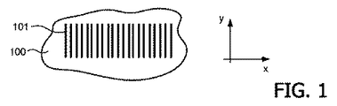
図1は、パターン構造が実質的に直線から成る基板層構造100を示し、これはx方向に改良された柔軟性をもたらす(座標系を参照)。図示の通り、スリットは、硬いプリント基板(PCB)、又は柔軟性フォイル、又は変形可能材料であり得る基板層構造にスリットをエッチングする/切り入れることによって形成される。そして、1つ又は複数の電子機器、例えば温度感受性素子が、例えばスリット101において、又は層構造100において、パターン構造に取り付けられ、はんだ付けされ、搭載され得る。特定の実施形態において、温度感受性素子(例えばサーミスタ)はスリットの間に搭載されることができる。こうしたセンサは、例えば関節又はその付近の指又は腕において、多数の温度を測定するために有用となり得る。
FIG. 1 shows a
図2はパターン構造が実質的に平行なS字型スリットから成る基板層構造100を示す。従って、x方向に改良された柔軟性に加えて、y方向の柔軟性が同時に実現され、従って改良された"伸縮性"をもたらす。ここでもやはり、1つ又は複数の電子機器が、例えばS字型スリット210において、又は層構造100において、パターン構造に取り付けられ得る。
FIG. 2 shows a
図3は、パターン構造がスパイラル形状を持つ単一スリット301から成る基板層構造100を示す。こうしたスパイラルな切り込みは、x‐y‐方向両方において、特にスパイラルの内側の先端において高い柔軟性を生じる。加えて、こうしたスパイラル状構造は、例えば楕円又は円錐物体上にフィットするために、z方向(面外方向)に大幅な伸縮性をもたらす。
FIG. 3 shows a
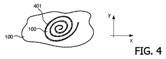
図4は、基板層構造100上に置かれる、従って最上層401を形成する、二重スパイラル又は"入れ子"スリット401を示す。こうした二重スパイラルスリットの使用は、一例として極めて柔軟性で自己整合性の二層センサ構造の容易な実装を可能にする。こうした構造は、例えば熱絶縁層で分離される2つ以上の温度感受性素子(サーミスタ、熱電対など)から成るいわゆるゼロ熱流束型(又は関連)センサなどの多層構造を作るのに非常に有用となり得、ここでは複数の温度測定値を組み合わせることによって深部体温が推定される。特に、絶縁層の両側における温度の差(測定される身体と周囲からの熱流束に比例する)が推定に使用されている。いくつかの実施形態において、身体から周囲への熱流束は、推定精度を増すために、加熱素子、蒸発器、可変有効熱伝導率の層などの使用によって随意に調節されることができる。従って、"入れ子"スリットの使用は、単一基板シートから多層構造の低コスト製造を可能にし、加えて異なる層を整列させる問題を簡略化する。
FIG. 4 shows a double spiral or “nested” slit 401 that rests on the
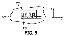
図5乃至図7はカム状構造を形成するスリットの3つの実施形態を示す。図5において構造501と502は基板層構造100の中に異なる深さを持ち、従ってx‐y‐方向に柔軟性かつ伸縮性である二層センサ構造を可能にする、すなわち、電子機器が各構造501、502の各々の中に置かれることができる。
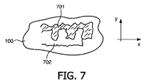
5-7 show three embodiments of slits that form a cam-like structure. In FIG. 5,
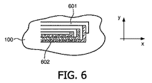
図6は構造が基板層構造100の上に置かれる"入れ子"カム状構造を示す。図7は、さらなる柔軟性と伸縮性が実現されるように、カム状スリットとS字型スリット701、702の組み合わせを示す。'入れ子'という語は単に、複数の'サブ平面'を作ることを可能にすることを意味する。
FIG. 6 shows a “nested” cam-like structure in which the structure is placed on the
図8は温度センサを形成する柔軟性かつ伸縮性のセンサアセンブリの一実施例を示す。基板層100は"入れ子"スパイラルであり、そこに複数の温度センサ(サーミスタ)802が取り付けられる。スパイラルの他の部分もまた、絶縁層801a及び801bの間にあるサーミスタ804を含む(上部801bと下部801aの間の暗い分離部)。スパイラルの両部分は、数ピースの駆動電子機器803に接続される。
FIG. 8 illustrates one embodiment of a flexible and stretchable sensor assembly that forms a temperature sensor. The
電子部品を有する任意の医療センサが、解剖学的適合を改良するために提案されたようなスリットを使用することで多いに利益を得ることに留意すべきである。 It should be noted that any medical sensor with electronic components will often benefit from using slits as proposed to improve anatomical fit.
開示された実施形態の特定の具体的詳細は、本発明の明瞭かつ完全な理解をもたらすために、限定ではなく説明を目的として記載される。しかしながら、本発明は、この開示の精神と範囲から著しく逸脱することなく、明細書に記載された詳細に厳密に一致しない他の実施形態において実施されてもよいことが、当業者に理解されるべきである。さらに、この文脈において、及び簡潔さと明瞭さを目的として、周知の装置、回路、及び方法の詳細な説明は、不必要な詳細と起こり得る混乱を避けるために省略されている。 Certain specific details of the disclosed embodiment are set forth for purposes of explanation rather than limitation, so as to provide a clear and thorough understanding of the present invention. However, one of ordinary skill in the art appreciates that the invention may be practiced in other embodiments that do not closely correspond to the details described in the specification without departing significantly from the spirit and scope of this disclosure. Should. Further, in this context and for purposes of brevity and clarity, detailed descriptions of well-known devices, circuits, and methods have been omitted to avoid unnecessary detail and possible confusion.
参照符号が請求項に含まれるが、参照符号の包含は明瞭さのために過ぎず、請求項の範囲を限定するものと解釈されるべきではない。 Reference signs are included in the claims, but the inclusion of the reference signs is only for clarity reasons and should not be construed as limiting the scope of the claims.
Claims (7)
柔軟な前記基板層構造の表面は、1つ以上のスリットによって形成される予め固定された形状のパターン構造であり、前記形状は、前記基板層構造の伸縮性がその下の前記身体表面の形状に適合するように選択される、基板層構造。 A substrate layer structure adapted to carry sensors, actuators, electronic components, or combinations thereof, and adapted to be attached to the surface of a human or animal body or biological species,
The flexible surface of the substrate layer structure is a pattern structure of a pre-fixed shape formed by one or more slits, and the shape is the shape of the body surface below the stretchability of the substrate layer structure Substrate layer structure selected to fit.
1つ以上の実質的に平行な直線スリット、又は、
1つ以上の実質的に平行なS字型スリット、又は、
スパイラル状スリット、又は、
二重スパイラル状スリット、又は、
多重スパイラル状スリット、又は、
カム状構造を形成するスリット、又は、
2つ以上のスパイラル状スリットの組み合わせ、
少なくとも1つのS字型スリットと、カム状構造を形成する少なくとも1つのスリットの組み合わせ、
上記のうちの2つ以上の組み合わせ、
によって形成される、請求項1に記載の基板層構造。 The pattern structure of the pre-fixed shape is
One or more substantially parallel linear slits, or
One or more substantially parallel S-shaped slits, or
Spiral slit, or
Double spiral slit, or
Multiple spiral slits, or
A slit forming a cam-like structure, or
A combination of two or more spiral slits,
A combination of at least one S-shaped slit and at least one slit forming a cam-like structure;
A combination of two or more of the above,
The substrate layer structure according to claim 1, formed by:
前記基板層構造を備えるステップと、
前記基板層構造の前記表面に、前記予め固定された形状の1つ以上のスリットを形成するステップと、
前記センサ、アクチュエータ、電子部品、又はそれらの組み合わせを、前記基板層構造に置くステップ又は取り付けるステップとを有する方法。 A method for manufacturing a substrate layer structure according to claim 1, comprising:
Providing the substrate layer structure;
Forming one or more slits of the pre-fixed shape on the surface of the substrate layer structure;
Placing or attaching the sensor, actuator, electronic component, or combination thereof to the substrate layer structure.
Applications Claiming Priority (3)
| Application Number | Priority Date | Filing Date | Title |
|---|---|---|---|
| EP08156802.4 | 2008-05-23 | ||
| EP08156802 | 2008-05-23 | ||
| PCT/IB2009/052044 WO2009141780A1 (en) | 2008-05-23 | 2009-05-18 | A substrate layer adapted to carry sensors, actuators or electrical components |
Related Child Applications (1)
| Application Number | Title | Priority Date | Filing Date |
|---|---|---|---|
| JP2014196356A Division JP5913509B2 (en) | 2008-05-23 | 2014-09-26 | A substrate layer adapted to carry a sensor, actuator or electrical component |
Publications (1)
| Publication Number | Publication Date |
|---|---|
| JP2011523863A true JP2011523863A (en) | 2011-08-25 |
Family
ID=40912064
Family Applications (2)
| Application Number | Title | Priority Date | Filing Date |
|---|---|---|---|
| JP2011510078A Pending JP2011523863A (en) | 2008-05-23 | 2009-05-18 | A substrate layer adapted to carry a sensor, actuator or electrical component |
| JP2014196356A Active JP5913509B2 (en) | 2008-05-23 | 2014-09-26 | A substrate layer adapted to carry a sensor, actuator or electrical component |
Family Applications After (1)
| Application Number | Title | Priority Date | Filing Date |
|---|---|---|---|
| JP2014196356A Active JP5913509B2 (en) | 2008-05-23 | 2014-09-26 | A substrate layer adapted to carry a sensor, actuator or electrical component |
Country Status (7)
| Country | Link |
|---|---|
| US (1) | US9587991B2 (en) |
| EP (1) | EP2280638B1 (en) |
| JP (2) | JP2011523863A (en) |
| CN (1) | CN102036600B (en) |
| BR (1) | BRPI0908620A2 (en) |
| RU (1) | RU2506890C2 (en) |
| WO (1) | WO2009141780A1 (en) |
Cited By (2)
| Publication number | Priority date | Publication date | Assignee | Title |
|---|---|---|---|---|
| JP2016506281A (en) * | 2013-01-08 | 2016-03-03 | エムシー10 インコーポレイテッドMc10,Inc. | Application of surface property monitoring |
| CN114136203A (en) * | 2021-11-12 | 2022-03-04 | 中国科学院金属研究所 | Preparation method of flexible strain sensor with high sensitivity and good cycling stability |
Families Citing this family (42)
| Publication number | Priority date | Publication date | Assignee | Title |
|---|---|---|---|---|
| US8366692B2 (en) | 2008-01-08 | 2013-02-05 | Richard Scott Weston | Sustained variable negative pressure wound treatment and method of controlling same |
| WO2009114624A2 (en) | 2008-03-12 | 2009-09-17 | Bluesky Medical Group Inc. | Negative pressure dressing and method of using same |
| US9068895B2 (en) | 2009-04-15 | 2015-06-30 | 3M Innovative Properties Company | Deep tissue temperature probe constructions |
| EP2419006B1 (en) | 2009-04-15 | 2015-09-30 | 3M Innovative Properties Company | Deep tissue temperature probe constructions |
| US8226294B2 (en) | 2009-08-31 | 2012-07-24 | Arizant Healthcare Inc. | Flexible deep tissue temperature measurement devices |
| CN102687154B (en) | 2009-12-28 | 2016-12-07 | 皇家飞利浦电子股份有限公司 | A kind of system of the beginning of the exacerbation of symptoms for predicting patient |
| BR112012015632A2 (en) | 2009-12-28 | 2018-04-10 | Koninklijke Philips Electronics N.V. | "system for providing a patient exercise training plan and computer-implemented method for providing a patient exercise training plan" |
| US8292495B2 (en) | 2010-04-07 | 2012-10-23 | Arizant Healthcare Inc. | Zero-heat-flux, deep tissue temperature measurement devices with thermal sensor calibration |
| US8292502B2 (en) | 2010-04-07 | 2012-10-23 | Arizant Healthcare Inc. | Constructions for zero-heat-flux, deep tissue temperature measurement devices |
| US9354122B2 (en) | 2011-05-10 | 2016-05-31 | 3M Innovative Properties Company | Zero-heat-flux, deep tissue temperature measurement system |
| US9869594B2 (en) * | 2012-11-05 | 2018-01-16 | Steamist, Inc. | Controller for steam bath having multiple temperature sensors |
| GB201317746D0 (en) | 2013-10-08 | 2013-11-20 | Smith & Nephew | PH indicator |
| FR3005562A1 (en) * | 2013-05-15 | 2014-11-21 | Ophtimalia | FLEXIBLE PASSIVE SENSOR FOR CONTACT LENS |
| WO2016025430A1 (en) * | 2014-08-11 | 2016-02-18 | The Board Of Trustees Of The University Of Illinois | Epidermal photonic systems and methods |
| JP6759526B2 (en) | 2015-02-27 | 2020-09-23 | セイコーエプソン株式会社 | Heat flow meter and electronic equipment |
| TWI634702B (en) * | 2016-05-11 | 2018-09-01 | 財團法人工業技術研究院 | Structure constructed by sheet |
| CA3023772A1 (en) | 2016-05-13 | 2017-11-16 | Smith & Nephew Plc | Sensor enabled wound monitoring and therapy apparatus |
| US10444912B2 (en) | 2016-12-30 | 2019-10-15 | Industrial Technology Research Institute | Sensing method of sensing device and stretchable sensor device |
| US11324424B2 (en) | 2017-03-09 | 2022-05-10 | Smith & Nephew Plc | Apparatus and method for imaging blood in a target region of tissue |
| EP3592212B1 (en) | 2017-03-09 | 2024-08-07 | Smith & Nephew plc | Wound dressing |
| US11406326B2 (en) | 2017-03-14 | 2022-08-09 | Mordehy HABER | Method, system and device for noninvasive core body temperature monitoring |
| SG11201909449TA (en) | 2017-04-11 | 2019-11-28 | Smith & Nephew | Component positioning and stress relief for sensor enabled wound dressings |
| US12033738B2 (en) | 2017-05-15 | 2024-07-09 | Smith & Nephew Plc | Negative pressure wound therapy system using eulerian video magnification |
| WO2018210692A1 (en) | 2017-05-15 | 2018-11-22 | Smith & Nephew Plc | Wound analysis device and method |
| EP3641627B1 (en) | 2017-06-23 | 2023-05-31 | Smith & Nephew PLC | Positioning of sensors for sensor enabled wound monitoring or therapy |
| GB201804502D0 (en) | 2018-03-21 | 2018-05-02 | Smith & Nephew | Biocompatible encapsulation and component stress relief for sensor enabled negative pressure wound therapy dressings |
| GB201809007D0 (en) | 2018-06-01 | 2018-07-18 | Smith & Nephew | Restriction of sensor-monitored region for sensor-enabled wound dressings |
| CN111093726B (en) | 2017-08-10 | 2023-11-17 | 史密夫及内修公开有限公司 | Sensor positioning for performing wound monitoring or treatment of sensors |
| GB201718870D0 (en) | 2017-11-15 | 2017-12-27 | Smith & Nephew Inc | Sensor enabled wound therapy dressings and systems |
| GB201804971D0 (en) | 2018-03-28 | 2018-05-09 | Smith & Nephew | Electrostatic discharge protection for sensors in wound therapy |
| US11759144B2 (en) | 2017-09-10 | 2023-09-19 | Smith & Nephew Plc | Systems and methods for inspection of encapsulation and components in sensor equipped wound dressings |
| GB201718859D0 (en) | 2017-11-15 | 2017-12-27 | Smith & Nephew | Sensor positioning for sensor enabled wound therapy dressings and systems |
| JP7282079B2 (en) | 2017-09-27 | 2023-05-26 | スミス アンド ネフュー ピーエルシー | PH Sensing for Sensor-Enabled Negative Pressure Wound Monitoring and Therapy Devices |
| US11839464B2 (en) | 2017-09-28 | 2023-12-12 | Smith & Nephew, Plc | Neurostimulation and monitoring using sensor enabled wound monitoring and therapy apparatus |
| EP3709943B1 (en) | 2017-11-15 | 2024-07-24 | Smith & Nephew PLC | Integrated sensor enabled wound monitoring and/or therapy dressings and systems |
| EP3849401A1 (en) | 2018-09-12 | 2021-07-21 | Smith & Nephew plc | Device, apparatus and method of determining skin perfusion pressure |
| GB201820927D0 (en) | 2018-12-21 | 2019-02-06 | Smith & Nephew | Wound therapy systems and methods with supercapacitors |
| GB2616370B (en) | 2019-03-18 | 2023-12-06 | Smith & Nephew | Design rules for sensor integrated substrates |
| GB201914443D0 (en) | 2019-10-07 | 2019-11-20 | Smith & Nephew | Sensor enabled negative pressure wound monitoring apparatus with different impedances inks |
| CN111904395B (en) * | 2020-07-24 | 2022-04-01 | 厦门大学 | Flexible base material for physiological information sensing and manufacturing method thereof |
| US12089952B2 (en) * | 2020-07-28 | 2024-09-17 | Xsensor Technology Corporation | Foot sensor and other sensor pads |
| US11534086B2 (en) | 2020-10-30 | 2022-12-27 | Medtronic Minimed, Inc. | Low-profile wearable medical device |
Citations (9)
| Publication number | Priority date | Publication date | Assignee | Title |
|---|---|---|---|---|
| JPS58172809A (en) * | 1982-04-02 | 1983-10-11 | 株式会社日立製作所 | Wiring structure using flexible circuit board |
| JPS6220393A (en) * | 1985-07-18 | 1987-01-28 | 松下電工株式会社 | Printed wiring board |
| JPH0311786A (en) * | 1989-06-09 | 1991-01-21 | Ibiden Co Ltd | Printed wiring board |
| JPH06246857A (en) * | 1993-02-25 | 1994-09-06 | Sharp Corp | Flexible film base |
| JPH09201338A (en) * | 1996-01-26 | 1997-08-05 | Hiromichi Omura | Flexible living body information signal generating device |
| JPH11219623A (en) * | 1998-02-03 | 1999-08-10 | Japan Aviation Electronics Ind Ltd | Flexible wiring member having high degree of freedom for wiring arrangement |
| JP2006520528A (en) * | 2003-03-19 | 2006-09-07 | ヒルシュマン エレクトロニクス ゲゼルシャフト ミット ベシュレンクテル ハフツング ウント コンパニー コマンディートゲゼルシャフト | Curved circuit board of antenna amplifier for vehicle antenna device |
| JP2007080929A (en) * | 2005-09-12 | 2007-03-29 | Lenovo Singapore Pte Ltd | Keyboard wiring structure and computer |
| JP2007209428A (en) * | 2006-02-08 | 2007-08-23 | Matsushita Electric Ind Co Ltd | Instrument and system for measuring biological information |
Family Cites Families (33)
| Publication number | Priority date | Publication date | Assignee | Title |
|---|---|---|---|---|
| JPH033283Y2 (en) * | 1984-12-27 | 1991-01-29 | ||
| DE3633803C2 (en) * | 1985-10-22 | 1995-10-19 | Telectronics Nv | Defibrillator electrode |
| FR2704417A1 (en) * | 1993-03-23 | 1994-11-04 | Mclaughlin James A | Device with profiled electrode (s) for the detection of bioelectric signals. |
| RU2138192C1 (en) * | 1995-03-06 | 1999-09-27 | Полартекникс, Лтд. | Method of identification of tissue type and apparatus for method embodiment |
| US6385473B1 (en) * | 1999-04-15 | 2002-05-07 | Nexan Limited | Physiological sensor device |
| DE29907768U1 (en) | 1999-05-03 | 1999-11-25 | Paul Rüster & Co. Inhaber U. Nowak GmbH, 14532 Stahnsdorf | Flexible surface temperature sensor |
| US6512512B1 (en) | 1999-07-31 | 2003-01-28 | Litton Systems, Inc. | Touch panel with improved optical performance |
| US6454725B1 (en) * | 2000-05-12 | 2002-09-24 | Chu Yih Yu | Thermometer for body temperature detection |
| US7181261B2 (en) * | 2000-05-15 | 2007-02-20 | Silver James H | Implantable, retrievable, thrombus minimizing sensors |
| AU2002212848A1 (en) * | 2000-10-09 | 2002-04-22 | Neuronz Limited | Sensor assembly for monitoring an infant brain |
| US6567680B2 (en) * | 2001-02-02 | 2003-05-20 | Medical Data Electronics | Disposable electro-cardiogram transmitter device and electrode node placement facilitator |
| JP4418120B2 (en) * | 2001-03-12 | 2010-02-17 | グローリー株式会社 | Fingerprint sensor, fingerprint collation device, and method of manufacturing fingerprint sensor |
| AU2002255953A1 (en) | 2001-03-27 | 2002-10-08 | Aron Z. Kain | Wireless system for measuring distension in flexible tubes |
| US6847913B2 (en) * | 2001-10-04 | 2005-01-25 | The Johns Hopkins University | Ambulatory surface skin temperature monitor |
| JP4157914B2 (en) * | 2002-03-20 | 2008-10-01 | 坂野 數仁 | Temperature measuring apparatus and temperature measuring method |
| US20050226310A1 (en) * | 2002-03-20 | 2005-10-13 | Sanyo Electric Co., Ltd. | Adhesive clinical thermometer pad and temperature measuring pad |
| JP2004024551A (en) * | 2002-06-26 | 2004-01-29 | Renesas Technology Corp | Semiconductor device for sensor system |
| WO2004092581A1 (en) * | 2003-04-15 | 2004-10-28 | Board Of Trustees Operating Michigan State University | Prestrained thin-film shape memory actuator using polymeric substrates |
| FR2858758B1 (en) * | 2003-08-14 | 2006-04-07 | Tam Telesante Sarl | MEDICAL MONITORING SYSTEM USING A CLOTHING |
| US20070001796A1 (en) * | 2003-08-26 | 2007-01-04 | Eberhardt Waffenschmidt | Printed circuit board with integrated inductor |
| JP2005137456A (en) * | 2003-11-04 | 2005-06-02 | Nitto Denko Corp | Electrode device to be mounted on body |
| US6964205B2 (en) * | 2003-12-30 | 2005-11-15 | Tekscan Incorporated | Sensor with plurality of sensor elements arranged with respect to a substrate |
| JP4463653B2 (en) * | 2004-05-10 | 2010-05-19 | 株式会社フジクラ | Hybrid sensor |
| US7768391B2 (en) * | 2004-09-03 | 2010-08-03 | Semiconductor Energy Laboratory Co., Ltd. | Health data collecting system and semiconductor device |
| JP2006108431A (en) * | 2004-10-06 | 2006-04-20 | Sharp Corp | Semiconductor device |
| JP2007053248A (en) * | 2005-08-18 | 2007-03-01 | Tdk Corp | Flexible substrate, mounting structure, display unit and portable electronic device |
| US8032210B2 (en) | 2005-10-06 | 2011-10-04 | Spinematrix, Inc. | EMG diagnostic system and method |
| US7712373B2 (en) * | 2006-03-03 | 2010-05-11 | Nagle H Troy | Sensor device for real-time monitoring or relative movement using capacitive fabric sensors |
| CA2538940A1 (en) * | 2006-03-03 | 2006-06-22 | James W. Haslett | Bandage with sensors |
| JP4143653B2 (en) * | 2006-05-24 | 2008-09-03 | オムロン株式会社 | Array type capacitive sensor |
| JP4805773B2 (en) * | 2006-09-20 | 2011-11-02 | シチズンホールディングス株式会社 | Electronic thermometer |
| US8238996B2 (en) * | 2006-12-05 | 2012-08-07 | Tyco Healthcare Group Lp | Electrode array |
| JP5295584B2 (en) * | 2008-02-14 | 2013-09-18 | 国立大学法人 筑波大学 | Blood flow measuring device and brain activity measuring device using blood flow measuring device |
-
2009
- 2009-05-18 CN CN200980118549.8A patent/CN102036600B/en active Active
- 2009-05-18 JP JP2011510078A patent/JP2011523863A/en active Pending
- 2009-05-18 EP EP09750237.1A patent/EP2280638B1/en active Active
- 2009-05-18 WO PCT/IB2009/052044 patent/WO2009141780A1/en active Application Filing
- 2009-05-18 BR BRPI0908620A patent/BRPI0908620A2/en not_active Application Discontinuation
- 2009-05-18 US US12/992,321 patent/US9587991B2/en active Active
- 2009-05-18 RU RU2010152667/14A patent/RU2506890C2/en active
-
2014
- 2014-09-26 JP JP2014196356A patent/JP5913509B2/en active Active
Patent Citations (9)
| Publication number | Priority date | Publication date | Assignee | Title |
|---|---|---|---|---|
| JPS58172809A (en) * | 1982-04-02 | 1983-10-11 | 株式会社日立製作所 | Wiring structure using flexible circuit board |
| JPS6220393A (en) * | 1985-07-18 | 1987-01-28 | 松下電工株式会社 | Printed wiring board |
| JPH0311786A (en) * | 1989-06-09 | 1991-01-21 | Ibiden Co Ltd | Printed wiring board |
| JPH06246857A (en) * | 1993-02-25 | 1994-09-06 | Sharp Corp | Flexible film base |
| JPH09201338A (en) * | 1996-01-26 | 1997-08-05 | Hiromichi Omura | Flexible living body information signal generating device |
| JPH11219623A (en) * | 1998-02-03 | 1999-08-10 | Japan Aviation Electronics Ind Ltd | Flexible wiring member having high degree of freedom for wiring arrangement |
| JP2006520528A (en) * | 2003-03-19 | 2006-09-07 | ヒルシュマン エレクトロニクス ゲゼルシャフト ミット ベシュレンクテル ハフツング ウント コンパニー コマンディートゲゼルシャフト | Curved circuit board of antenna amplifier for vehicle antenna device |
| JP2007080929A (en) * | 2005-09-12 | 2007-03-29 | Lenovo Singapore Pte Ltd | Keyboard wiring structure and computer |
| JP2007209428A (en) * | 2006-02-08 | 2007-08-23 | Matsushita Electric Ind Co Ltd | Instrument and system for measuring biological information |
Cited By (2)
| Publication number | Priority date | Publication date | Assignee | Title |
|---|---|---|---|---|
| JP2016506281A (en) * | 2013-01-08 | 2016-03-03 | エムシー10 インコーポレイテッドMc10,Inc. | Application of surface property monitoring |
| CN114136203A (en) * | 2021-11-12 | 2022-03-04 | 中国科学院金属研究所 | Preparation method of flexible strain sensor with high sensitivity and good cycling stability |
Also Published As
| Publication number | Publication date |
|---|---|
| EP2280638A1 (en) | 2011-02-09 |
| CN102036600A (en) | 2011-04-27 |
| RU2010152667A (en) | 2012-06-27 |
| RU2506890C2 (en) | 2014-02-20 |
| US9587991B2 (en) | 2017-03-07 |
| CN102036600B (en) | 2014-08-06 |
| JP2015052598A (en) | 2015-03-19 |
| WO2009141780A1 (en) | 2009-11-26 |
| JP5913509B2 (en) | 2016-04-27 |
| BRPI0908620A2 (en) | 2016-06-14 |
| US20110069459A1 (en) | 2011-03-24 |
| EP2280638B1 (en) | 2016-12-21 |
Similar Documents
| Publication | Publication Date | Title |
|---|---|---|
| JP5913509B2 (en) | A substrate layer adapted to carry a sensor, actuator or electrical component | |
| WO2009141777A1 (en) | A substrate layer adapted to carry sensors, actuators or electrical components | |
| JP6506653B2 (en) | Stretchable wiring board | |
| JP6488189B2 (en) | Elastic wiring board | |
| JP7154508B2 (en) | Wiring board and method for manufacturing wiring board | |
| CN102487577B (en) | Manufacturing method of circuit board with combination of flexible circuit board and hard circuit board | |
| JP6812033B2 (en) | Electrode belt device for measuring biological signals | |
| JP2020010052A5 (en) | ||
| JP2015052598A5 (en) | ||
| EP3697485B1 (en) | High-volume manufacturing of catheters comprising electrodes having low impedance at low frequency | |
| AU2015285996A1 (en) | Sensor device having a flexible electrical conductor structure | |
| US11523514B2 (en) | Method for fabrication of a soft-matter printed circuit board | |
| US10398024B2 (en) | Stretchable circuit board and method for manufacturing stretchable circuit board | |
| CN109429426B (en) | Multilayer circuit fabric material for integrating electronic element and manufacturing method thereof | |
| US11982572B2 (en) | Stick-on thermometer | |
| US9560746B1 (en) | Stress relief for rigid components on flexible circuits | |
| JP2017022173A (en) | Elastic conductive substrate and elastic conductive laminate | |
| CN110769610A (en) | Preparation method of electronic device and multi-mode electronic sensor | |
| JP7067011B2 (en) | Wiring board and manufacturing method of wiring board | |
| US11910531B2 (en) | Flexible printed circuit board having a battery mounted thereto | |
| CN107027248B (en) | Manufacturing method of rigid-flexible combined circuit board and rigid-flexible combined circuit board | |
| JP2009224358A (en) | Flexible printed wiring board and optical transmission/reception module | |
| JP4934867B2 (en) | Thermocouple sensor substrate and manufacturing method thereof | |
| KR20180049765A (en) | Electronic device | |
| Lu et al. | Stretchability, conformability, and low-cost manufacture of epidermal sensors |
Legal Events
| Date | Code | Title | Description |
|---|---|---|---|
| A621 | Written request for application examination |
Free format text: JAPANESE INTERMEDIATE CODE: A621 Effective date: 20120516 |
|
| A977 | Report on retrieval |
Free format text: JAPANESE INTERMEDIATE CODE: A971007 Effective date: 20130930 |
|
| A131 | Notification of reasons for refusal |
Free format text: JAPANESE INTERMEDIATE CODE: A131 Effective date: 20131003 |
|
| A601 | Written request for extension of time |
Free format text: JAPANESE INTERMEDIATE CODE: A601 Effective date: 20131216 |
|
| A602 | Written permission of extension of time |
Free format text: JAPANESE INTERMEDIATE CODE: A602 Effective date: 20131224 |
|
| A521 | Written amendment |
Free format text: JAPANESE INTERMEDIATE CODE: A523 Effective date: 20140324 |
|
| A131 | Notification of reasons for refusal |
Free format text: JAPANESE INTERMEDIATE CODE: A131 Effective date: 20140626 |
|
| A02 | Decision of refusal |
Free format text: JAPANESE INTERMEDIATE CODE: A02 Effective date: 20150106 |