JP2011512630A - Optical device and manufacturing method - Google Patents
Optical device and manufacturing method Download PDFInfo
- Publication number
- JP2011512630A JP2011512630A JP2010547103A JP2010547103A JP2011512630A JP 2011512630 A JP2011512630 A JP 2011512630A JP 2010547103 A JP2010547103 A JP 2010547103A JP 2010547103 A JP2010547103 A JP 2010547103A JP 2011512630 A JP2011512630 A JP 2011512630A
- Authority
- JP
- Japan
- Prior art keywords
- light
- light guide
- light extraction
- optical device
- layer
- Prior art date
- Legal status (The legal status is an assumption and is not a legal conclusion. Google has not performed a legal analysis and makes no representation as to the accuracy of the status listed.)
- Pending
Links
Images


Classifications
-
- G—PHYSICS
- G02—OPTICS
- G02B—OPTICAL ELEMENTS, SYSTEMS OR APPARATUS
- G02B6/00—Light guides; Structural details of arrangements comprising light guides and other optical elements, e.g. couplings
- G02B6/0001—Light guides; Structural details of arrangements comprising light guides and other optical elements, e.g. couplings specially adapted for lighting devices or systems
- G02B6/0011—Light guides; Structural details of arrangements comprising light guides and other optical elements, e.g. couplings specially adapted for lighting devices or systems the light guides being planar or of plate-like form
- G02B6/0033—Means for improving the coupling-out of light from the light guide
- G02B6/0035—Means for improving the coupling-out of light from the light guide provided on the surface of the light guide or in the bulk of it
- G02B6/0036—2-D arrangement of prisms, protrusions, indentations or roughened surfaces
-
- Y—GENERAL TAGGING OF NEW TECHNOLOGICAL DEVELOPMENTS; GENERAL TAGGING OF CROSS-SECTIONAL TECHNOLOGIES SPANNING OVER SEVERAL SECTIONS OF THE IPC; TECHNICAL SUBJECTS COVERED BY FORMER USPC CROSS-REFERENCE ART COLLECTIONS [XRACs] AND DIGESTS
- Y10—TECHNICAL SUBJECTS COVERED BY FORMER USPC
- Y10T—TECHNICAL SUBJECTS COVERED BY FORMER US CLASSIFICATION
- Y10T29/00—Metal working
- Y10T29/49—Method of mechanical manufacture
Landscapes
- Physics & Mathematics (AREA)
- General Physics & Mathematics (AREA)
- Optics & Photonics (AREA)
- Planar Illumination Modules (AREA)
- Light Guides In General And Applications Therefor (AREA)
Abstract
光学装置はライトガイドとライトガイドを照明するための光源とを備える。ライトガイドは透明基板層と透明層とを備える。ライトガイドは基板層の表面上に光取出し面を有する。透明層は光取出し面に対向する基板層表面上に配置され、または、透明層は基板層の光取出し面上に配置される。透明層は光取出し改善手段を含む。さらに、ライトガイドの製造方法が提供される。 The optical device includes a light guide and a light source for illuminating the light guide. The light guide includes a transparent substrate layer and a transparent layer. The light guide has a light extraction surface on the surface of the substrate layer. The transparent layer is disposed on the surface of the substrate layer facing the light extraction surface, or the transparent layer is disposed on the light extraction surface of the substrate layer. The transparent layer includes light extraction improving means. Furthermore, a light guide manufacturing method is provided.
Description
本発明は、ライトガイドと、ライトガイドを照明するための光源とを備える光学装置に関する。さらに、本発明は、ライトガイドの製造方法に関する。 The present invention relates to an optical device including a light guide and a light source for illuminating the light guide. Furthermore, the present invention relates to a method for manufacturing a light guide.
本発明の第1の目的は、非常に薄く、さらに、均一な光取出しを提供するライトガイドを備える改善された光学装置を提供することにある。本発明の第2の目的は、そのための製造方法を提供することにある。 It is a first object of the present invention to provide an improved optical device that is very thin and further comprises a light guide that provides uniform light extraction. The second object of the present invention is to provide a manufacturing method therefor.
第1および第2の目的は、ライトガイドと、ライトガイドを照明するための光源とを備える光学装置に関する本発明の一態様によって実現され、ここで、前記ライトガイドは、透明基板層と、透明層とを備え、前記ライトガイドは前記基板層上の光取出し面を備え、前記透明層は前記光取出し面に対向する前記基板層表面上に配され、または、前記透明層は前記基板層の前記光取出し面上に配され、前記透明層は光取出し改善手段を含む。 The first and second objects are realized by an aspect of the present invention relating to an optical device including a light guide and a light source for illuminating the light guide, wherein the light guide includes a transparent substrate layer, a transparent substrate layer, and a transparent substrate layer. The light guide includes a light extraction surface on the substrate layer, the transparent layer is disposed on the surface of the substrate layer facing the light extraction surface, or the transparent layer is formed on the substrate layer. The transparent layer is disposed on the light extraction surface, and includes a light extraction improving means.
透明基板層と透明層とを備え、当該透明層が光取出し改善手段を含むライトガイドにより、均一な光取出しを示す非常に薄いライトガイドが提供されうる。これにより、ライトガイドの光取出しは、光取出し面全体にわたってその度合いがほぼ同じになるように最適化される。 A light guide comprising a transparent substrate layer and a transparent layer, the transparent layer including light extraction improving means, can provide a very thin light guide exhibiting uniform light extraction. Thereby, the light extraction of the light guide is optimized so that the degree thereof is substantially the same over the entire light extraction surface.
ライトガイドは、好ましくは300μm未満、特に好ましくは100μm未満の厚さを有する。 The light guide preferably has a thickness of less than 300 μm, particularly preferably less than 100 μm.
本光学装置はキーパッドまたはディスプレイのバックライトとして有利に使用可能である。好ましくは、本光学装置は、携帯電話機用キーパッドあるいはLCD(液晶表示装置)のためのバックライトとして用いられる。従って、本光学装置が、非常に薄く、高い光学効率を有し、光取出し面の全体にわたって非常に均一であることが利点である。 The optical device can be advantageously used as a keypad or display backlight. Preferably, the optical device is used as a keypad for a mobile phone or a backlight for an LCD (Liquid Crystal Display). Thus, it is an advantage that the present optical device is very thin, has high optical efficiency, and is very uniform over the entire light extraction surface.
本発明の好ましい一実施形態において、光源は、ライトガイドの側面に配される。 In a preferred embodiment of the present invention, the light source is disposed on the side of the light guide.
光源の光は、従って、側面からライトガイドに出力される。よって、端部照明式のライトガイドが提供される。それゆえ、本光学装置は、ライトガイドの後ろまたは前に配置される光源を備える光学装置と比較して非常に薄い。側面からライトガイドに結合される光源を備える光学装置の厚さは、そのようにしてさらに減らすことができる。 The light from the light source is therefore output from the side to the light guide. Thus, an end illumination type light guide is provided. The optical device is therefore very thin compared to an optical device with a light source arranged behind or in front of the light guide. The thickness of the optical device with the light source coupled from the side to the light guide can thus be further reduced.
透明層は、光取出し改善手段を含む。ここで、光取出し改善手段は、透明層に沿ってその密度が可変である。例えば、光取出し改善手段は、プリズムアレイである。 The transparent layer includes light extraction improving means. Here, the density of the light extraction improving means is variable along the transparent layer. For example, the light extraction improving means is a prism array.
光取出し改善手段の使用により、ライトガイドの光取出しの均一性を最適化可能である。最適化された光取出し改善手段は、例えば発光ダイオード(LED)のような点光源、または、ライトガイドのいずれかの側面に設けられる線光源について、最適化されるよう密度を変化させることができる。当該光取出し改善手段は、均一なバックライトを発生するよう、好ましくは正確に光を取り出す。 By using the light extraction improving means, it is possible to optimize the light extraction uniformity of the light guide. The optimized light extraction improving means can change the density to be optimized for a point light source such as a light emitting diode (LED) or a line light source provided on either side of the light guide. . The light extraction improving means preferably extracts light accurately so as to generate a uniform backlight.
光取出し改善手段は、例えば、球面状、錐体状、または三角状の孔またはバンプである。あるいは、光取出し改善手段は、拡散散乱手段、特に、エッチングされたドットであってもよい。 The light extraction improving means is, for example, a spherical, conical, or triangular hole or bump. Alternatively, the light extraction improving means may be a diffuse scattering means, in particular an etched dot.
透明層は、好ましくは硬化性層であり、ここで、該透明層は好ましくはUV放射により硬化可能である。好ましくは、透明層は、ポリマー層である。 The transparent layer is preferably a curable layer, wherein the transparent layer is preferably curable by UV radiation. Preferably, the transparent layer is a polymer layer.
透明基板層は、好ましくは、プラスチックフィルムである。本発明の特に好ましい実施形態では、透明層の材料は、基板層の材料に一致した屈折率を有する。それゆえ、有利に薄く、柔軟なライトガイドが提供されうる。 The transparent substrate layer is preferably a plastic film. In a particularly preferred embodiment of the invention, the material of the transparent layer has a refractive index that matches the material of the substrate layer. Therefore, an advantageously thin and flexible light guide can be provided.
本発明の好ましい一実施形態において、複数の光源が、ライトガイドの少なくとも一側面上に配置される。複数の光源は、好ましくは、ライトガイドの均一な光取出しを最適化することができる。 In a preferred embodiment of the present invention, a plurality of light sources are arranged on at least one side of the light guide. The multiple light sources are preferably capable of optimizing the uniform light extraction of the light guide.
本発明の特に好ましい一実施形態において、ライトガイドは、一つの光源または複数の光源をライトガイドに光学的に接続する手段を含む。一つの光源または複数の光源をライトガイドに光学的に接続する手段は、例えば、ライトガイドの切り欠きであってもよい。切り欠きは、例えば、くぼみよりなるドームが可能である。 In one particularly preferred embodiment of the invention, the light guide includes means for optically connecting a light source or light sources to the light guide. The means for optically connecting one light source or a plurality of light sources to the light guide may be, for example, a notch in the light guide. The cutout can be, for example, a dome consisting of a depression.
ライトガイドの製造方法は、
−透明基板層を設けすステップと、
−前記透明基板の光取出し面に対向する表面上に透明層を配置し、または、前記基板層の光取出し面上に透明層を配置するステップと、
−前記透明層の上に光取出し改善手段を形成するステップと、
−前記ライトガイドの一面上に少なくとも1つの光源を取り付けるステップと、
を有する。
The light guide manufacturing method is
-Providing a transparent substrate layer;
-Disposing a transparent layer on the surface opposite to the light extraction surface of the transparent substrate, or disposing a transparent layer on the light extraction surface of the substrate layer;
-Forming light extraction improving means on the transparent layer;
-Mounting at least one light source on one side of the light guide;
Have
このようにして、有利に、薄い、さらに均一な光取出しを提供するライトガイドが製造可能である。ライトガイドは、例えば、好ましくはバックライトとして用いられる。ライトガイドは、キーパッドまたはディスプレイのバックライトとして、特に好ましくは携帯電話機用キーパッドまたはLCDのバックライトとして有利に用いられる。 In this way, a light guide that advantageously provides a thin and more uniform light extraction can be produced. The light guide is preferably used as a backlight, for example. The light guide is advantageously used as a keypad or display backlight, particularly preferably as a mobile phone keypad or LCD backlight.
ライトガイドは、好ましくは、厚さ300μm、特に好ましくは、厚さ100μm未満である。 The light guide is preferably 300 μm thick, particularly preferably less than 100 μm thick.
光取出し改善手段は、好ましくは、UV放射により硬化される。本発明の好ましい一実施形態において、光取出し改善手段は、透明層上にエンボス加工により形成される。好ましくは、光取出し改善手段は、ロールツーロール法により透明層上に形成される。 The light extraction improving means is preferably cured by UV radiation. In a preferred embodiment of the present invention, the light extraction improving means is formed on the transparent layer by embossing. Preferably, the light extraction improving means is formed on the transparent layer by a roll-to-roll method.
光取出し改善手段のための原型は、複製されて、ロールツーロール法に組み込まれてもよい。従って、透明基板層の大量の材料ロールを、大量生産に使用可能なライトガイドの製造に用いることができる。よって、ライトガイドの製造は、射出成形されたライトガイドなどと比較して非常に経済的であり、非常にコスト効率がよい。なお、原型はエッチングにより製造可能である。 The prototype for the light extraction improving means may be duplicated and incorporated into the roll-to-roll process. Therefore, a large amount of material roll of the transparent substrate layer can be used for manufacturing a light guide that can be used for mass production. Thus, the manufacture of light guides is very economical and very cost effective compared to injection molded light guides and the like. The prototype can be manufactured by etching.
本発明の好ましい一実施形態において、光源をライトガイドに光学的に接続する手段は、例えば、打ち抜きまたはレーザーカットにより、ライトガイド内に形成される。 In a preferred embodiment of the invention, the means for optically connecting the light source to the light guide is formed in the light guide, for example by stamping or laser cutting.
それゆえ、ライトガイドは、光源をライトガイドに光学的に接続する手段、特に、切り欠きを含む。この切り欠きは、例えばエンボス加工された材料シートの大ロールから打ち抜かれ、レーザーカットされ、または他の方法でカットされてもよい。ライトガイドの切り欠きは、例えば、ドームとして形成されてもよい。 The light guide therefore includes means for optically connecting the light source to the light guide, in particular notches. This notch may be punched, for example, from a large roll of embossed material sheet, laser cut, or otherwise cut. The notch of the light guide may be formed as a dome, for example.
本発明は、例示的実施形態および関連する図1〜5に基づいて、以下より詳細に説明される。図面は、縮尺は実際のものではない概略図に基づいて本発明の異なる例示的実施形態を示す。同一の要素または同様に機能する要素は、図面中同一の参照記号により示される。 The invention will be described in more detail below on the basis of exemplary embodiments and the related FIGS. The drawings illustrate different exemplary embodiments of the present invention based on schematic diagrams that are not to scale. Identical or similarly functioning elements are indicated by the same reference symbols in the drawings.
図1は、ライトガイド1a、1bと、ライトガイド1a、1bを照明するための光源2とを備える光学装置の断面図を示す。
FIG. 1 shows a cross-sectional view of an optical device including light guides 1a and 1b and a
光源2は、ライトガイド1a、1bの一側面上に配置される。好ましくは、光源2は、発光ダイオード(LED)である。
The
他の照明ランプと比較して、LEDの光源としての使用には光学装置(光源と組み合わされたライトガイド)の寸法が小さいという利点がある。本光学装置の有利な特徴の1つは、これが非常に薄く形成できることである。このことは、本光学装置を非常に薄いバックライトシステム、例えば、携帯電話機用キーパッドまたはLCDに使用することを可能にする。 Compared to other illumination lamps, the use of LEDs as a light source has the advantage that the dimensions of the optical device (light guide combined with the light source) are small. One advantageous feature of the present optical device is that it can be made very thin. This allows the optical device to be used in a very thin backlight system, such as a cell phone keypad or LCD.
光源2は、好ましくは、例えば、青、黄、緑または赤のスペクトル範囲の波長を有する光を発する。CIE色空間では、好ましい発光は、例えばだいたい、x=0.18、y=0.12("クリスタルブルー");x=0.16、y=0.20("ブルーラグーン");x=0.16、y=0.34("グリーンラグーン");x=0.40、y=0.44("クリスタルイエロー");x=0.29、y=0.17("マゼンタ");または、x=0.38、y=0.24("クリスタルピンク")の色座標の色点を有する。従って、広い色スペクトルの中から6色のバラエティーが可能であり、不飽和色の専用の組が提供される。
The
光源2の発光は、好ましくは側面からライトガイド1a、1bに結合される。この場合、ライトガイドは、端部照明式のライトガイドである。それゆえ、光学装置は、ライトガイドの後または前に配置された光源を備える光学装置と比較して、非常に薄い。端部照明式のライトガイドを備える光学装置の厚さは、そのようにしてさらに削減されうる。
The light emission of the
ライトガイド1a、1bは、透明基板層1aと透明層1bとを備える。さらに、ライトガイドは、光取出し面5を基板層1aの表面上に有する。透明層1bは、基板層1aの光取出し面5に対向する面上に配置される。さらに、透明層1bは、光取出し改善手段3を含む。
The light guides 1a and 1b include a
ライトガイド1a、1bが、透明基板層1aと、光取出し改善手段3を含む透明層1bとを備えることにより、ライトガイドの均一な光取出しが提供される。光取出しは、これにより、光取出し面5全体にわたってライトガイド1a、1bの光取出しがほぼ同一であるように最適化される。
Since the light guides 1a and 1b include the
ライトガイド1a、1bは、300μm未満の厚さD、好ましくは100μm未満の厚さDを有する。このように薄いライトガイド1a、1bは、キーパッドまたはディスプレイのバックライトとして有利に使用可能である。好ましくは、ライトガイド1a、1bは、携帯電話機用キーパッドまたはLCDのバックライトとして用いられる。従って、ライトガイド1a、1bは、一方で薄く、高い光効率を有し、他方で光取出し面5全体にわたって非常に均一であることが非常に重要である。
The light guides 1a and 1b have a thickness D of less than 300 μm, preferably a thickness D of less than 100 μm. Such thin light guides 1a and 1b can be advantageously used as a keypad or display backlight. Preferably, the light guides 1a and 1b are used as a cellular phone keypad or an LCD backlight. Therefore, it is very important that the light guides 1a, 1b are thin on the one hand and have high light efficiency, and on the other hand are very uniform over the entire
透明層1bは、光取出し改善手段3を含む。光取出し改善手段3は、好ましくは、光取出し面5に光を反射または分散する。光取出し改善手段3を用いることにより、ライトガイド1a、1bの光取出しの均一性が最適化される。ライトガイドの光取出しの効率はこのように増大される。
The
好ましくは、光取出し改善手段3は、透明層1bに沿ってその密度を変化させる。光取出し改善手段3は、例えば発光ダイオード(LED)のような点光源2またはライトガイド1a、1bのいずれかの面での線光源について最適化されるよう密度が有利に可変である。好ましくは、光取出し改善手段3の密度は、光源2からの距離内で増加する。それゆえ、光取出し改善手段3は、均一なバックライトを形成するため、好ましくは均一に光を取り出す。
Preferably, the light extraction improving means 3 changes the density along the
例えば、光取出し改善手段3はプリズムアレイである。特に、光取出し改善手段3は、例えば球面状、錐体状、または三角状の孔またはバンプである。これに代えて、光取出し改善手段3は、拡散散乱のための手段、特に、エッチングされたドットであってもよい。ライトガイド1a、1bの本例示的実施形態では、光取出し改善手段3は、基板層1aに対向する透明層1bの面上に配置された球面状の孔である。
For example, the light extraction improving means 3 is a prism array. In particular, the light extraction improving means 3 is, for example, a spherical, conical, or triangular hole or bump. Alternatively, the light extraction improving means 3 may be a means for diffuse scattering, particularly an etched dot. In the present exemplary embodiment of the light guides 1a and 1b, the light extraction improving means 3 is a spherical hole arranged on the surface of the
光取出し改善手段3は好ましくは透明層1b上にエンボス加工により形成される。好ましくは、光取出し改善手段3は透明層1b上にロールツーロール法により形成される。
The light extraction improving means 3 is preferably formed on the
光取出し改善手段3の原型は、複製され、ロールツーロール法に組み込まれてもよい。従って、透明基板層1aの大量の材料ロールが、ライトガイド1a、1bを大量生産するのに用いられる。これにより、ライトガイド1a、1bは、射出成形されるライトガイドなどと比較して非常に経済的かつ非常にコスト効率が高い。
The prototype of the light extraction improving means 3 may be duplicated and incorporated into the roll-to-roll method. Therefore, a large amount of material roll of the
基板層1aと透明層1bの材料は、光源2の発光に対して光学的に透過性である。
The materials of the
透明層1bは有利には硬化性層である。透明層1bは好ましくはUV放射により硬化可能である。好ましくは、透明層はポリマー層である。
The
透明基板層1aは好ましくはプラスチックフィルムである。特に、透明層1bの材料は、基板層1aの材料と一致する屈折率を有するか、または、同様の屈折率を有する。それゆえ、良好な光誘導を示す、好ましくは薄く柔軟なライトガイド1a、1bが提供される。
The
ライトガイド1a、1b内の光伝播を、図1および2中、矢印によって示す。 Light propagation in the light guides 1a and 1b is indicated by arrows in FIGS.
好ましくは、光学装置は、ライトガイド1a、1bの光取出し面5に対向して配置される反射層4を備える。それゆえ、ライトガイド1a、1bの光効率は改善される。
Preferably, the optical device includes a
図2は、ライトガイド1a、1bと、ライトガイド1a、1bを照明する光源2とを備える光学装置の他の断面を概略的に示す。
FIG. 2 schematically shows another cross section of the optical device including the light guides 1a and 1b and the
図1の実施形態とは異なり、ライトガイドがキャリア6、例えばリードフレーム、コードまたはプリント配線板の上に取り付けられる。それゆえ、ライトガイド1a、1bおよび光源2はキャリア6上に配置されることができ、さらに光源2の電気接続が形成される。
Unlike the embodiment of FIG. 1, the light guide is mounted on a carrier 6, such as a lead frame, cord or printed wiring board. Therefore, the light guides 1a, 1b and the
ライトガイド1a、1bとキャリア6との間には、反射層4が配置される。それゆえ、取り出された光は、反射層4により反射され、光取出し面5上から出力される。ライトガイド1a、1bの効率は、このようにして好ましく増大させうる。
A
図1の実施形態とは異なり、2つの光源2がライトガイド1a、1bの側面上に配置される。特に、光源2は互いに対向して配置される。このような配置は、好ましい均一な光取出しをもたらす。ライトガイド1a、1bの光取出し度は、光取出し面5全体にわたって大きく変化しない。
Unlike the embodiment of FIG. 1, two
ライトガイド1a、1bの取出し均一性を最適化するため、光取出し改善手段3が、基板層1aに対向する透明層1bの表面上に配置される。図2の実施形態の光取出し改善手段3は、光源2への距離に依存してその密度が変わる錐体状の孔である。
In order to optimize the extraction uniformity of the light guides 1a and 1b, the light extraction improving means 3 is arranged on the surface of the
図3は、ライトガイド1a、1bと、ライトガイド1a、1bを照明するための光源2とを備える他の光学装置の概略平面図を示す。
FIG. 3 shows a schematic plan view of another optical device including light guides 1a and 1b and a
この実施形態では、ライトガイド1a、1bは光源2をライトガイド1a、1bに光学的に接続する手段7を含む。光学的接続手段7は、打ち抜きまたはレーザーカットによりライトガイド1a、1b内に形成される。
In this embodiment, the light guides 1a, 1b include means 7 for optically connecting the
光学的接続手段7は、例えば、ライトガイドの切り欠きであってもよい。切り欠きは、くぼみよりなるドームであってもよい。好ましくは、光源2は、発光が大きな光損失なしにライトガイド1a、1bに入力されるよう、ドーム内に部分的に配置される。
The optical connecting means 7 may be, for example, a light guide notch. The cutout may be a dome made of a depression. Preferably, the
さらに、光取出し構造9が、好ましくはライトガイド1a、1bの光取出し面5に設けられる。これらの光取出し構造9は、例えば、3次元構造である。光取出し構造9は、ライトガイド1a、1bから出力される光の均一性と効率とを増大させる。また、光取出し面5を粗面化して、光取出しの均一性および効率をさらに上昇させてもよい。
Furthermore, a
図3の光学装置の実施形態は、上記の相違を除き、図1および2の光学装置の実施形態の主な特徴を備える。 The optical device embodiment of FIG. 3 comprises the main features of the optical device embodiment of FIGS. 1 and 2, except for the differences described above.
図4は、ライトガイド1a、1bとライトガイド1a、1bを照明する光源2とを備える他の光学装置の概略平面図を示す。
FIG. 4 is a schematic plan view of another optical device including the light guides 1a and 1b and the
光学装置1a、1bの本実施形態は、ライトガイド1a、1bの側面に配置される複数の光源2を備える。特に、2つの光源2、特にLED、は、ライトガイド1a、1bの一側面上に配置される。この側面に対向する側面に2つの他のLED2が配置されている。それゆえ、この場合、2つのLED2は互いに対向して配置されている。
This embodiment of the
複数の光源2はライトガイド1a、1bの均一な光取出しを最適化しうる。好ましくは、複数のLED2は、ライトガイドの両側面に配置されている。特に、少なくとも2つのLEDがライトガイドの各側面に、例えば、互いに対向して配置されていてもよい。このようにして、光学的に均一な光取出しがもたらされる。ライトガイド1a、1bの光取出しは、これにより、光取出し面5全体にわたってほぼ同一である。
The plurality of
図4の光学装置の実施形態は、上記相違を除き、図1、2および3の光学装置の実施形態の主な特徴を備える。 The optical device embodiment of FIG. 4 comprises the main features of the optical device embodiments of FIGS.
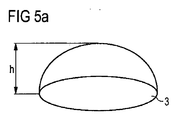
図5A、5B、5Cに、光取出し改善手段3の好ましい概略平面図を示す。
5A, 5B and 5C show preferred schematic plan views of the light
図5Aに球面状の孔を示す。球面状の孔は、例えば、約15μmの高さhを有する。球面状の孔の断面の寸法は約50μmである。 FIG. 5A shows a spherical hole. The spherical hole has, for example, a height h of about 15 μm. The dimension of the cross section of the spherical hole is about 50 μm.
図5Bの光取出し改善手段3は、3次元の四辺形プリズム状の孔である。四辺形プリズム孔の底面の各側辺長は、例えば、約71μmである。四辺形プリズムの高さhは、図5Aの例の高さと同様に、約15μmである。四辺形プリズムの底面と2つの対向する側面との間の角度αは約45°である。 The light extraction improving means 3 in FIG. 5B is a three-dimensional quadrangular prism-shaped hole. Each side length of the bottom surface of the quadrangular prism hole is, for example, about 71 μm. The height h of the quadrilateral prism is about 15 μm, similar to the height in the example of FIG. 5A. The angle α between the bottom surface of the quadrilateral prism and the two opposite side surfaces is about 45 °.
図5Cに錐体状の孔を示す。図5Bの例と等しく、底面の側辺の長さは約71μmであり、高さhは約15μmである。底面と各側面との間の角度αは、それぞれの場合約45°である。 FIG. 5C shows a cone-shaped hole. As in the example of FIG. 5B, the length of the side of the bottom surface is about 71 μm and the height h is about 15 μm. The angle α between the bottom and each side is in each case about 45 °.
図5A〜5Cの例に基づく光取出し改善手段3の使用により、ライトガイドの光取出しの均一性が最適化されうる。このような光取出し改善手段3は、均一なバックライトを形成するために、光を好ましくは均一に取り出す。 By using the light extraction improving means 3 based on the example of FIGS. 5A-5C, the light extraction uniformity of the light guide can be optimized. Such light extraction improving means 3 preferably extracts light uniformly in order to form a uniform backlight.
光取出し改善手段3は、好ましくはエンボス加工により透明層上に形成される。好ましくは、光取出し改善手段3はロールツーロール法により透明層上に形成される。 The light extraction improving means 3 is preferably formed on the transparent layer by embossing. Preferably, the light extraction improving means 3 is formed on the transparent layer by a roll-to-roll method.
図6は、ライトガイド1a、1bと、ライトガイド1a、1bを照明するための光源2とを備える他の光学装置の断面を概略的に示す。
FIG. 6 schematically shows a cross section of another optical device including light guides 1a and 1b and a
図1の実施形態と比して、透明層1bが透明基板1aの光取出し面5上に配置される。
Compared with the embodiment of FIG. 1, the
ライトガイド1a、1bの本例示的実施形態において、光取出し改善手段3は、基板層1aに対向する透明層1bの表面上に配置される球面状のバンプである。
In the present exemplary embodiment of the light guides 1a and 1b, the light extraction improving means 3 is a spherical bump disposed on the surface of the
本特許出願は米国仮特許出願61/066,719の優先権を主張し、その開示内容は本明細書中に参照により組み込まれる。 This patent application claims priority to US provisional patent application 61 / 066,719, the disclosure of which is incorporated herein by reference.
例示的実施形態を用いる本発明の上記詳細な説明は、本発明のこれへの限定を意味すると理解されるべきではない。むしろ、クレーム1および11において定められた発明の概念は、きわめて多くの非常に異なるデザインに適用可能である。特に、本発明は、その組み合わせが特許クレームの対象に挙げられていないとしても、例示的実施形態および残りの詳細な説明において示された特徴のすべての組み合わせをも包含する。 The above detailed description of the invention using exemplary embodiments should not be taken as implying a limitation on the invention. Rather, the inventive concepts defined in claims 1 and 11 are applicable to a great many very different designs. In particular, the invention encompasses all combinations of features shown in the exemplary embodiments and the remaining detailed description, even though that combination is not listed in the subject of the patent claims.
Claims (15)
−前記ライトガイドは透明基板層と透明層とを備え、
−前記ライトガイドは前記基板層の表面上に光取出し面を有し、
−前記透明層は前記基板層の前記光取出し面に対向する表面上に配置されるか、または、前記基板層の前記光取出し面上に配置され、
−前記透明層は光取出し改善手段を含む、
ことを特徴とする光学装置。 An optical device comprising a light guide and a light source for illuminating the light guide,
The light guide comprises a transparent substrate layer and a transparent layer;
The light guide has a light extraction surface on the surface of the substrate layer;
The transparent layer is disposed on a surface of the substrate layer facing the light extraction surface, or is disposed on the light extraction surface of the substrate layer;
The transparent layer comprises light extraction improving means,
An optical device.
−透明層を前記基板層の光取出し面に対向する表面上に配置するか、または、透明層を前記基板層の光取出し面上に配置するステップと、
−光取出し改善手段を前記透明層上に形成するステップと、
−該ライトガイドの面上に光源を取り付けるステップと、
有することを特徴とする、ライトガイドの製造方法。 Providing a transparent substrate layer;
-Placing the transparent layer on the surface of the substrate layer facing the light extraction surface, or disposing the transparent layer on the light extraction surface of the substrate layer;
-Forming light extraction improving means on the transparent layer;
-Mounting a light source on the surface of the light guide;
A method for manufacturing a light guide, comprising:
Applications Claiming Priority (2)
| Application Number | Priority Date | Filing Date | Title |
|---|---|---|---|
| US6671908P | 2008-02-22 | 2008-02-22 | |
| PCT/EP2009/001165 WO2009103517A1 (en) | 2008-02-22 | 2009-02-18 | Optical arrangement and production method |
Publications (2)
| Publication Number | Publication Date |
|---|---|
| JP2011512630A true JP2011512630A (en) | 2011-04-21 |
| JP2011512630A5 JP2011512630A5 (en) | 2012-03-01 |
Family
ID=40750824
Family Applications (1)
| Application Number | Title | Priority Date | Filing Date |
|---|---|---|---|
| JP2010547103A Pending JP2011512630A (en) | 2008-02-22 | 2009-02-18 | Optical device and manufacturing method |
Country Status (6)
| Country | Link |
|---|---|
| US (1) | US20110110116A1 (en) |
| EP (1) | EP2245363A1 (en) |
| JP (1) | JP2011512630A (en) |
| KR (1) | KR20100124754A (en) |
| CN (1) | CN101946120A (en) |
| WO (1) | WO2009103517A1 (en) |
Families Citing this family (10)
| Publication number | Priority date | Publication date | Assignee | Title |
|---|---|---|---|---|
| WO2010003273A1 (en) * | 2008-07-08 | 2010-01-14 | 海立尔股份有限公司 | Flexible backlight module |
| KR20110080165A (en) * | 2008-10-17 | 2011-07-12 | 루미너스 디바이시즈, 아이엔씨. | Remote lighting assemblies and methods |
| KR101587551B1 (en) * | 2009-12-17 | 2016-01-21 | 삼성전자주식회사 | 3 3 Waveguide plate for 3D image display and 3D image display apparatus employing the same |
| TWI520839B (en) * | 2010-07-20 | 2016-02-11 | 國立成功大學 | Method for manufacturing a flexible optical plate and flexible optical plate fabricated by the method, and backlight module using the flexible optical plate |
| DE112013002944T5 (en) | 2012-06-13 | 2015-02-19 | Innotec, Corp. | Flexible hollow fiber optic cable |
| US9632230B2 (en) * | 2014-05-05 | 2017-04-25 | Continental Automotive Systems, Inc. | Light guide assembly for display illumination |
| WO2015184456A1 (en) * | 2014-05-30 | 2015-12-03 | Osram Sylvania Inc. | Light control films and lighting devices including same |
| FR3032512B1 (en) * | 2015-02-05 | 2020-01-17 | Valeo Vision | LIGHT GUIDE WITH MEANS OF COMPENSATING FOR PROGRESSIVE LOSS OF LIGHT ALONG THE GUIDE |
| CN104913270A (en) * | 2015-06-30 | 2015-09-16 | 四川长虹电器股份有限公司 | Ultra-thin light-guide plate used for mark of electronic product |
| DE102019204061B4 (en) * | 2019-03-25 | 2023-03-23 | Volkswagen Aktiengesellschaft | Component with at least one backlit surface |
Citations (8)
| Publication number | Priority date | Publication date | Assignee | Title |
|---|---|---|---|---|
| JPH0955111A (en) * | 1995-08-15 | 1997-02-25 | Minebea Co Ltd | Manufacture of board used for surface light source device |
| JP2000147218A (en) * | 1998-11-06 | 2000-05-26 | Hitachi Chem Co Ltd | Planar light emitter and planar light emitter unit |
| JP2000284280A (en) * | 1999-03-29 | 2000-10-13 | Rohm Co Ltd | Surface light source |
| JP2005062541A (en) * | 2003-08-14 | 2005-03-10 | Alps Electric Co Ltd | Optical member and its manufacturing method, and surface emitting device and liquid crystal display device |
| JP2007149587A (en) * | 2005-11-30 | 2007-06-14 | Optrex Corp | Backlight device |
| JP2007535790A (en) * | 2004-04-30 | 2007-12-06 | オイ モディリス リミテッド | Ultra thin lighting element |
| JP2008010393A (en) * | 2006-05-30 | 2008-01-17 | Hitachi Maxell Ltd | Backlight unit and liquid crystal display device |
| JP2008218207A (en) * | 2007-03-05 | 2008-09-18 | Mitsubishi Rayon Co Ltd | Light guide plate, composite optical sheet, and surface light source |
Family Cites Families (22)
| Publication number | Priority date | Publication date | Assignee | Title |
|---|---|---|---|---|
| GB2196100B (en) * | 1986-10-01 | 1990-07-04 | Mitsubishi Rayon Co | Light diffusing device |
| JP3199504B2 (en) * | 1993-02-09 | 2001-08-20 | 富士通株式会社 | Lighting equipment |
| US20040135273A1 (en) * | 1995-06-27 | 2004-07-15 | Parker Jeffery R. | Methods of making a pattern of optical element shapes on a roll for use in making optical elements on or in substrates |
| US6712481B2 (en) * | 1995-06-27 | 2004-03-30 | Solid State Opto Limited | Light emitting panel assemblies |
| JP4159059B2 (en) * | 1998-06-05 | 2008-10-01 | シチズン電子株式会社 | Planar light source unit |
| US6827456B2 (en) * | 1999-02-23 | 2004-12-07 | Solid State Opto Limited | Transreflectors, transreflector systems and displays and methods of making transreflectors |
| EP1167872A4 (en) * | 1999-03-29 | 2002-07-31 | Rohm Co Ltd | Planar light source |
| JP4023079B2 (en) * | 2000-08-31 | 2007-12-19 | 株式会社日立製作所 | Planar illumination device and display device including the same |
| TWI297093B (en) * | 2000-09-25 | 2008-05-21 | Mitsubishi Rayon Co | Light source device |
| US6811274B2 (en) * | 2002-12-04 | 2004-11-02 | General Electric Company | Polarization sensitive optical substrate |
| US7537369B2 (en) * | 2003-02-28 | 2009-05-26 | Sharp Kabushiki Kaisha | Surface radiation conversion element, liquid crystal display device, and method of producing a surface radiation conversion element |
| KR100865607B1 (en) * | 2003-05-07 | 2008-10-27 | 히다치 가세고교 가부시끼가이샤 | Hologram optical element and surface light source device using it |
| WO2006031545A1 (en) * | 2004-09-09 | 2006-03-23 | Fusion Optix, Inc. | Enhanced lcd backlight |
| TWI403546B (en) * | 2004-09-30 | 2013-08-01 | Oji Holdings Corp | Method for producing foamed product |
| WO2006052755A2 (en) * | 2004-11-04 | 2006-05-18 | Solid State Opto Limited | Long curved wedges in an optical film |
| KR100610336B1 (en) * | 2005-09-12 | 2006-08-09 | 김형준 | Light guide plate for backlight panel of keypad and its manufacturing method |
| US7955531B1 (en) * | 2006-04-26 | 2011-06-07 | Rohm And Haas Electronic Materials Llc | Patterned light extraction sheet and method of making same |
| JP3898217B1 (en) * | 2006-05-30 | 2007-03-28 | 日立マクセル株式会社 | Backlight unit and liquid crystal display device |
| US7876489B2 (en) * | 2006-06-05 | 2011-01-25 | Pixtronix, Inc. | Display apparatus with optical cavities |
| US7708442B2 (en) * | 2006-10-25 | 2010-05-04 | Honeywell International Inc. | Light emitting panels for display devices |
| WO2008117854A1 (en) * | 2007-03-27 | 2008-10-02 | Dai Nippon Printing Co., Ltd. | Sheet-shaped optical member, resin composition for optical sheet, optical sheet, and process for producing the optical sheet |
| TWI322281B (en) * | 2007-04-04 | 2010-03-21 | Eternal Chemical Co Ltd | Thin and flexible light guide element |
-
2009
- 2009-02-18 WO PCT/EP2009/001165 patent/WO2009103517A1/en active Application Filing
- 2009-02-18 EP EP09713509A patent/EP2245363A1/en not_active Withdrawn
- 2009-02-18 US US12/918,997 patent/US20110110116A1/en not_active Abandoned
- 2009-02-18 JP JP2010547103A patent/JP2011512630A/en active Pending
- 2009-02-18 CN CN200980105700.4A patent/CN101946120A/en active Pending
- 2009-02-18 KR KR1020107020195A patent/KR20100124754A/en not_active Application Discontinuation
Patent Citations (8)
| Publication number | Priority date | Publication date | Assignee | Title |
|---|---|---|---|---|
| JPH0955111A (en) * | 1995-08-15 | 1997-02-25 | Minebea Co Ltd | Manufacture of board used for surface light source device |
| JP2000147218A (en) * | 1998-11-06 | 2000-05-26 | Hitachi Chem Co Ltd | Planar light emitter and planar light emitter unit |
| JP2000284280A (en) * | 1999-03-29 | 2000-10-13 | Rohm Co Ltd | Surface light source |
| JP2005062541A (en) * | 2003-08-14 | 2005-03-10 | Alps Electric Co Ltd | Optical member and its manufacturing method, and surface emitting device and liquid crystal display device |
| JP2007535790A (en) * | 2004-04-30 | 2007-12-06 | オイ モディリス リミテッド | Ultra thin lighting element |
| JP2007149587A (en) * | 2005-11-30 | 2007-06-14 | Optrex Corp | Backlight device |
| JP2008010393A (en) * | 2006-05-30 | 2008-01-17 | Hitachi Maxell Ltd | Backlight unit and liquid crystal display device |
| JP2008218207A (en) * | 2007-03-05 | 2008-09-18 | Mitsubishi Rayon Co Ltd | Light guide plate, composite optical sheet, and surface light source |
Also Published As
| Publication number | Publication date |
|---|---|
| CN101946120A (en) | 2011-01-12 |
| WO2009103517A1 (en) | 2009-08-27 |
| EP2245363A1 (en) | 2010-11-03 |
| US20110110116A1 (en) | 2011-05-12 |
| KR20100124754A (en) | 2010-11-29 |
Similar Documents
| Publication | Publication Date | Title |
|---|---|---|
| JP2011512630A (en) | Optical device and manufacturing method | |
| KR101601646B1 (en) | Light guides | |
| US10151448B2 (en) | Display apparatus | |
| US7458714B2 (en) | Optical plate and backlight module using the same | |
| JP5809629B2 (en) | Optical waveguide | |
| US7527416B2 (en) | Light guide plate with diffraction gratings and backlight module using the same | |
| US20090180296A1 (en) | Logo display | |
| JP2018106826A (en) | Light guide plate, surface light source device, display device and electronic apparatus | |
| JP2016505898A (en) | Multi-beam grating-based backlighting | |
| TW201341728A (en) | Lighting device having a light guide structure | |
| US9110211B2 (en) | Light guide plate for plane light source, method for manufacturing the same, and plane light source unit using the same | |
| US20060120107A1 (en) | LED backlight module | |
| US7793448B1 (en) | Display module and illumination sign device using the same | |
| US7824092B2 (en) | Backlight module having a plurality of groups of concentric microstructures on reflective surface thereof | |
| US20120075883A1 (en) | Edge-type led backlight moudle | |
| JP2010505221A (en) | Optical waveguide and optical device | |
| TWI497016B (en) | Plane light source and flexible plane light source | |
| JP2008277157A (en) | Display device | |
| US9134476B2 (en) | LED module with light guiding plate | |
| KR20080057595A (en) | Flexible planar lighting device | |
| JP2006294560A (en) | Backlight | |
| JP2008027649A (en) | Light source apparatus and backlighting apparatus | |
| WO2012059855A1 (en) | Light emitting sheet | |
| CN114325920B (en) | Backlight, method of assembling the same, and display apparatus including the same | |
| TWI283774B (en) | Backlight module and light guide plate used therein |
Legal Events
| Date | Code | Title | Description |
|---|---|---|---|
| A521 | Request for written amendment filed |
Free format text: JAPANESE INTERMEDIATE CODE: A523 Effective date: 20120112 |
|
| A621 | Written request for application examination |
Free format text: JAPANESE INTERMEDIATE CODE: A621 Effective date: 20120112 |
|
| A977 | Report on retrieval |
Free format text: JAPANESE INTERMEDIATE CODE: A971007 Effective date: 20130711 |
|
| A131 | Notification of reasons for refusal |
Free format text: JAPANESE INTERMEDIATE CODE: A131 Effective date: 20130716 |
|
| A601 | Written request for extension of time |
Free format text: JAPANESE INTERMEDIATE CODE: A601 Effective date: 20131002 |
|
| A602 | Written permission of extension of time |
Free format text: JAPANESE INTERMEDIATE CODE: A602 Effective date: 20131015 |
|
| A02 | Decision of refusal |
Free format text: JAPANESE INTERMEDIATE CODE: A02 Effective date: 20140324 |