JP2011511928A - Shape measuring apparatus and method - Google Patents
Shape measuring apparatus and method Download PDFInfo
- Publication number
- JP2011511928A JP2011511928A JP2010523935A JP2010523935A JP2011511928A JP 2011511928 A JP2011511928 A JP 2011511928A JP 2010523935 A JP2010523935 A JP 2010523935A JP 2010523935 A JP2010523935 A JP 2010523935A JP 2011511928 A JP2011511928 A JP 2011511928A
- Authority
- JP
- Japan
- Prior art keywords
- laser
- shape measuring
- generated
- emitted
- shape
- Prior art date
- Legal status (The legal status is an assumption and is not a legal conclusion. Google has not performed a legal analysis and makes no representation as to the accuracy of the status listed.)
- Pending
Links
Images


Classifications
-
- G—PHYSICS
- G01—MEASURING; TESTING
- G01B—MEASURING LENGTH, THICKNESS OR SIMILAR LINEAR DIMENSIONS; MEASURING ANGLES; MEASURING AREAS; MEASURING IRREGULARITIES OF SURFACES OR CONTOURS
- G01B11/00—Measuring arrangements characterised by the use of optical techniques
- G01B11/24—Measuring arrangements characterised by the use of optical techniques for measuring contours or curvatures
- G01B11/2441—Measuring arrangements characterised by the use of optical techniques for measuring contours or curvatures using interferometry
-
- G—PHYSICS
- G01—MEASURING; TESTING
- G01B—MEASURING LENGTH, THICKNESS OR SIMILAR LINEAR DIMENSIONS; MEASURING ANGLES; MEASURING AREAS; MEASURING IRREGULARITIES OF SURFACES OR CONTOURS
- G01B11/00—Measuring arrangements characterised by the use of optical techniques
- G01B11/24—Measuring arrangements characterised by the use of optical techniques for measuring contours or curvatures
-
- G—PHYSICS
- G01—MEASURING; TESTING
- G01B—MEASURING LENGTH, THICKNESS OR SIMILAR LINEAR DIMENSIONS; MEASURING ANGLES; MEASURING AREAS; MEASURING IRREGULARITIES OF SURFACES OR CONTOURS
- G01B11/00—Measuring arrangements characterised by the use of optical techniques
-
- G—PHYSICS
- G01—MEASURING; TESTING
- G01B—MEASURING LENGTH, THICKNESS OR SIMILAR LINEAR DIMENSIONS; MEASURING ANGLES; MEASURING AREAS; MEASURING IRREGULARITIES OF SURFACES OR CONTOURS
- G01B9/00—Measuring instruments characterised by the use of optical techniques
- G01B9/02—Interferometers
-
- B—PERFORMING OPERATIONS; TRANSPORTING
- B82—NANOTECHNOLOGY
- B82Y—SPECIFIC USES OR APPLICATIONS OF NANOSTRUCTURES; MEASUREMENT OR ANALYSIS OF NANOSTRUCTURES; MANUFACTURE OR TREATMENT OF NANOSTRUCTURES
- B82Y35/00—Methods or apparatus for measurement or analysis of nanostructures
Abstract
【課題】段差の大きい場合にも被検体の形状を誤り無く測定し、機械的に基準面を位置移動させずとも迅速で正確に被検体の形状を測定することができる形状測定装置及びその方法を提供すること。
【解決手段】レーザー干渉計を用いたナノ形状測定装置及びその方法が開示される。複数のレーザー装置は、それぞれビームを生成し、生成されたビームのうち、特定周波数のビームを放出し、生成されたビームの波長を検出するための干渉信号を出力する。制御部は、出力された干渉信号から生成されたビームの波長を検出し、検出された波長に基づいて複数の前記レーザー装置を制御する。光学装置部は、被検体の表面にレーザー装置から放出されたビームを投射させて、被検体の干渉縞を生成する。複数のシャッターは、開閉可能であり、閉じた場合には、レーザー装置から放出されたビームが光学装置部に照射されるのを遮断する。撮像部は、生成された干渉縞を撮像する。本発明による形状測定装置及びその方法によれば、安定した周波数を放出する複数個の多チャネル周波数スキャニングレーザー装置を用いて光を放出するため、高さの大きい被検体の形状を正確で精密に測定することができる。また、本発明による形状測定装置及びその方法は、基準面の位置移動を要求せず、これにより、基準面の位置移動による時間所要及び誤差発生を防止し、被検体の形状を迅速で正確に測定することができる。
【選択図】図1An object of the present invention is to provide a shape measuring apparatus and method for measuring the shape of an object without error even when there is a large level difference and measuring the shape of the object quickly and accurately without mechanically moving the position of a reference surface. To provide.
An apparatus and method for measuring a nano shape using a laser interferometer is disclosed. Each of the plurality of laser devices generates a beam, emits a beam having a specific frequency among the generated beams, and outputs an interference signal for detecting the wavelength of the generated beam. The control unit detects the wavelength of the beam generated from the output interference signal, and controls the plurality of laser devices based on the detected wavelength. The optical device unit projects the beam emitted from the laser device onto the surface of the subject to generate interference fringes of the subject. The plurality of shutters can be opened and closed. When the shutters are closed, the optical device unit is blocked from being irradiated with the beam emitted from the laser device. The imaging unit images the generated interference fringes. According to the shape measuring apparatus and method according to the present invention, light is emitted using a plurality of multi-channel frequency scanning laser devices that emit stable frequencies, so that the shape of a subject having a large height can be accurately and accurately determined. Can be measured. In addition, the shape measuring apparatus and method according to the present invention do not require the position movement of the reference plane, thereby preventing the time requirement and the error due to the position movement of the reference plane, and the shape of the subject can be quickly and accurately. Can be measured.
[Selection] Figure 1
Description
形状測定装置及びその方法であって、より詳細には、光の干渉を通じてナノサイズの形状を測定するための形状測定装置及び方法に関するものである。 More particularly, the present invention relates to a shape measuring apparatus and method for measuring a nano-sized shape through light interference.
3次元形状測定装置とは、検査しようとする物体(以下、被検体という)の表面に、一定の形態を有する光を照射して干渉縞を形成し、この干渉縞を測定及び解析して物体表面の高さに関する情報を得る装置のことをいう。
このような測定方法は、被検体の3次元形状を容易に得ることができるので、医学、産業分野で広く用いられている。
特に最近の産業界全般における急速な技術発展に伴い、半導体、MEMS、平板ディスプレイ、光部品などの分野において微細加工が要求されており、現在はナノ単位の超精密製造技術が要求されている。
このような加工において必要な加工の形状も単なる2次元パターンから複雑な3次元形状に変化しており、よって、3次元微細形状を測定する技術の重要性はより増加してきている。
A three-dimensional shape measuring apparatus is an object in which interference fringes are formed by irradiating the surface of an object to be inspected (hereinafter referred to as a subject) with light having a certain form, and measuring and analyzing the interference fringes. A device that obtains information about the height of the surface.
Such a measuring method is widely used in the medical and industrial fields because the three-dimensional shape of the subject can be easily obtained.
In particular, with recent rapid technological development in the industry as a whole, fine processing is required in the fields of semiconductors, MEMS, flat panel displays, optical components, etc., and ultra-precision manufacturing technology in nano units is now required.
The shape of processing necessary for such processing has also changed from a simple two-dimensional pattern to a complicated three-dimensional shape, and therefore, the importance of a technique for measuring a three-dimensional fine shape is increasing.
従来は、このような3次元形状測定のために光位相遷移干渉計(PSI: Phase Shifting Interferometer)を用いた測定方法を使用していた。
光位相遷移干渉計(PSI)の基本的な測定原理について説明すると、次の通りである。光源からの照明光をそれぞれ基準面と測定面に照射した後、それらを光分割器を用いて合わせて、測定面の映像と縞状の干渉信号を獲得する。
その後、光検出素子で、発生する干渉信号の位相(Phase)を計算することによって高さを測定する。
このような位相干渉測定法は、干渉信号追跡法といい、干渉信号の間隔が光源波長の半波長に該当する点とその間の干渉信号変化を調和関数で補間することによって間接的に干渉信号の位相を計算する方法を用いたものである。
Conventionally, a measurement method using an optical phase shift interferometer (PSI) has been used for such three-dimensional shape measurement.
The basic measurement principle of the optical phase transition interferometer (PSI) will be described as follows. After irradiating the illumination light from the light source to the reference surface and the measurement surface, respectively, they are combined using a light splitter to obtain an image of the measurement surface and a striped interference signal.
Thereafter, the height is measured by calculating the phase of the generated interference signal with the light detection element.
Such a phase interference measurement method is called an interference signal tracking method, and the interference signal is indirectly detected by interpolating the interference signal interval corresponding to a half wavelength of the light source wavelength and a change in the interference signal between them with a harmonic function. A method for calculating the phase is used.
このような既存の光位相遷移干渉計(PSI)は、2πを測定モジュールロ(measured modulo)することによって、測定された位相データの間に2πの不一致を除去するために、隣接したピクセル間の光経路差(OPD: Optical Path Difference)の差は波長の半分であるとする。
これにより、既存の光位相遷移干渉計(PSI)は、被検体の表面勾配が、隣接したピクセル間の位相変化がπよりも大きくなる程度に十分に大きい場合は、位相測定結果が劣化するという問題点があった。
Such existing optical phase-shifting interferometers (PSI) measure 2 moduli by measuring 2 modulo between adjacent pixels in order to eliminate 2π mismatches between measured phase data. The optical path difference (OPD) difference is assumed to be half the wavelength.
As a result, the existing optical phase-shifting interferometer (PSI) says that the phase measurement result deteriorates when the surface gradient of the subject is sufficiently large so that the phase change between adjacent pixels is larger than π. There was a problem.
また、既存の光位相遷移干渉計(PSI)は、基準面を3回以上一定の位相だけ連続して動かしながら光検出素子により干渉縞を少なくとも3回以上測定して、基準光束の波頭面に対する測定光束の波頭面の相対的な位相差を比較することによって、被検体に対する表面の高さを測定することができる。
したがって、既存の光位相遷移干渉計(PSI)は、測定面の上部方向に基準面を一定の間隔で動かしながら動きながら測定しなければならず、測定に時間がかかり、機械的な移動により発生する位置上の誤差から、正確で精密に形状を測定することができなかった。
In addition, the existing optical phase transition interferometer (PSI) measures the interference fringes at least three times or more with the photodetecting element while continuously moving the reference surface by a certain phase three times or more, and the reference light beam with respect to the wave front surface. By comparing the relative phase difference of the wave front surface of the measurement light beam, the height of the surface relative to the subject can be measured.
Therefore, the existing optical phase transition interferometer (PSI) must be measured while moving while moving the reference plane at a constant interval in the upper direction of the measurement plane, and it takes time to measure and is caused by mechanical movement. The shape could not be measured accurately and precisely due to the error in the position to perform.
本発明は、位相遷移干渉計において段差の測定領域が波長の1/4に制限される限界を克服することによって、段差の大きい場合にも被検体の形状を誤り無く測定し、機械的に基準面を位置移動させずとも迅速で正確に被検体の形状を測定することができる形状測定装置及びその方法を提供することを技術的課題とする。 The present invention overcomes the limitation that the measurement area of the step in the phase transition interferometer is limited to ¼ of the wavelength, thereby accurately measuring the shape of the subject even when the step is large, and mechanically It is an object of the present invention to provide a shape measuring apparatus and method for measuring the shape of a subject quickly and accurately without moving the position of the surface.
上記課題を達成するために、本発明は、周波数を精密にスキャニングできるレーザーを用いて位相遷移された映像を得る方式で、機械的な位相遷移方法に取って代わる。
また、段差の測定領域を広めるために、異なる波長で2台の周波数スキャニングレーザーを用いる。
In order to achieve the above object, the present invention replaces the mechanical phase transition method by obtaining a phase-shifted image using a laser capable of precisely scanning the frequency.
Also, two frequency scanning lasers with different wavelengths are used to widen the measurement area of the step.
本発明による形状測定装置は、ビームを生成し、前記生成されたビームのうち特定周波数のビームを放出し、前記生成されたビームの波長を検出するための干渉信号を出力する複数のレーザー装置と;前記出力された干渉信号から、前記生成されたビームの波長を検出し、該検出された波長に基づいて複数の前記レーザー装置を制御する制御部と;を含む。 The shape measuring apparatus according to the present invention includes: a plurality of laser apparatuses that generate a beam, emit a beam having a specific frequency among the generated beams, and output an interference signal for detecting a wavelength of the generated beam; A control unit that detects a wavelength of the generated beam from the output interference signal and controls the plurality of laser devices based on the detected wavelength.
前記レーザー装置が、前記ビームを生成する半導体レーザーと;前記生成されたビームの波長を検出するための干渉信号を生成して出力する干渉信号生成部と;前記特定周波数を共振周波数として有し、前記生成されたビームが照射され、該照射されたビームの周波数と前記共振周波数とが同一の場合には、前記照射されたビームを前記半導体レーザーにフィードバックする外部反射体と;前記外部反射体が前記照射されたビームをフィードバックした場合には、前記生成されたビームを外部に放出する光伝達部と;を含む。
好ましくは、本発明に係る形状測定装置は、2個のレーザー装置を含む。
The laser device includes a semiconductor laser that generates the beam; an interference signal generation unit that generates and outputs an interference signal for detecting a wavelength of the generated beam; and the specific frequency as a resonance frequency; An external reflector that feeds back the irradiated beam to the semiconductor laser when the generated beam is irradiated and the frequency of the irradiated beam is the same as the resonance frequency; and A light transmission unit that emits the generated beam to the outside when the irradiated beam is fed back.
Preferably, the shape measuring device according to the present invention includes two laser devices.
前記制御部は、複数の前記レーザー装置を交互に稼働させ、該稼働するレーザー装置が4個の特定周波数のビームを放出するように制御する。
ここで、前記制御部は、前記レーザー装置の温度または前記レーザー装置に印加される電流を調節して前記レーザー装置を制御する。
The control unit operates a plurality of the laser devices alternately and controls the operating laser devices to emit four specific frequency beams.
Here, the control unit controls the laser device by adjusting a temperature of the laser device or a current applied to the laser device.
好ましくは、上記形状測定装置は、被検体の表面に前記放出されたビームを投射させて、前記被検体の干渉縞を生成する光学装置部と;開閉可能であり、閉じた場合には、前記放出されたビームが前記光学装置部に照射されるのを遮断する複数のシャッターと;前記生成された干渉縞を撮像する撮像部と;をさらに含む。
ここで、前記制御部は、前記複数のシャッターのうちいずれか一方のシャッターを開いて、前記放出されたビームを前記光学装置部に照射させ、前記特定周波数のビームのそれぞれに対する前記撮像された干渉縞を獲得する。
そして、前記制御部が、前記特定周波数及び前記特定周波数のビームのそれぞれに対して前記獲得された干渉縞に基づいて前記被検体の形状情報を算出する。
Preferably, the shape measuring device is capable of projecting the emitted beam onto the surface of the subject to generate an interference fringe of the subject; and openable and closable; And a plurality of shutters for blocking the emitted beam from being applied to the optical device unit; and an imaging unit for imaging the generated interference fringes.
Here, the control unit opens one of the plurality of shutters, irradiates the emitted beam to the optical device unit, and the captured interference with each of the beams of the specific frequency Earn stripes.
Then, the control unit calculates shape information of the subject based on the acquired interference fringes for each of the specific frequency and the beam of the specific frequency.
上記課題を解決するための本発明に係る形状測定方法は、複数のレーザー装置を用いて形状を測定する方法であって、前記複数のレーザー装置のうちいずれか一方のレーザー装置を稼働する第1稼働段階と;前記稼働したレーザー装置から複数の特定周波数のビームをそれぞれ放出させ、前記放出された特定周波数のビームのそれぞれを被検体に投射させて、前記特定周波数のそれぞれに対する前記被検体の干渉縞を獲得する干渉縞獲得段階と;前記稼働したレーザー装置を停止させ、複数のレーザー装置のうちいずれか他方のレーザー装置を稼働する第2稼働段階と;を含む。 A shape measuring method according to the present invention for solving the above-described problem is a method for measuring a shape using a plurality of laser devices, and is a first method for operating any one of the plurality of laser devices. An operation stage; a plurality of specific frequency beams are respectively emitted from the operated laser device, and each of the emitted specific frequency beams is projected onto a subject, and the subject interferes with each of the specific frequencies. An interference fringe acquisition step of acquiring fringes; and a second operation step of stopping the activated laser device and operating one of the plurality of laser devices.
前記第1稼働段階が、前記複数のレーザー装置のうちいずれか一方のレーザー装置に電流を印加する段階と;前記電流が印加されたレーザー装置から放出されるビームを遮断するシャッターを開く段階と;を含む。
また、前記干渉縞獲得段階は、前記稼働したレーザー装置を通じて特定周波数のビームを放出するビーム放出段階と;前記放出されたビームを被検体の表面に投射させて、前記被検体の干渉縞を獲得する段階と;を含む。
また、前記ビーム放出段階は、前記稼働したレーザー装置で生成されたビームの波長を検出する段階と;前記検出された波長に基づいて、前記レーザー装置に印加される電流を調節する段階と;前記ビームの共鳴周波数を検出する段階と;前記ビームの共鳴周波数が検出された場合には、前記ビームを前記特定周波数のビームとして放出する段階と;を含む。
そして、前記第2稼働段階が、前記稼働したレーザー装置から放出されるビームを遮断するシャッターを閉じる段階と;前記稼働したレーザー装置に印加される電流の供給を中断する段階と;前記複数のレーザー装置のうちいずれか他方のレーザー装置に電流を印加する段階と;前記電流の印加されたレーザー装置から放出されるビームを遮断するシャッターを開く段階と;を含むことを特徴とする。
The first operating step includes applying a current to one of the plurality of laser devices; opening a shutter that blocks a beam emitted from the laser device to which the current is applied; including.
The interference fringe acquisition step includes: a beam emission step of emitting a beam of a specific frequency through the activated laser device; and projecting the emitted beam onto the surface of the subject to obtain the interference fringe of the subject. And
The beam emitting step includes detecting a wavelength of a beam generated by the activated laser device; adjusting a current applied to the laser device based on the detected wavelength; Detecting a resonance frequency of the beam; and, if a resonance frequency of the beam is detected, emitting the beam as a beam of the specific frequency.
And the second operation stage includes a step of closing a shutter for blocking a beam emitted from the operated laser apparatus; a step of interrupting supply of current applied to the operated laser apparatus; and the plurality of lasers Applying a current to the other laser device of the device; and opening a shutter that blocks a beam emitted from the laser device to which the current is applied.
好ましくは、上記形状測定方法は、前記特定周波数及び前記特定周波数のビームから獲得された干渉縞に基づいて前記被検体の形状情報を算出する段階をさらに含む。 Preferably, the shape measurement method further includes a step of calculating shape information of the subject based on the specific frequency and interference fringes acquired from the beam of the specific frequency.
以下、添付の図面を参照しつつ、本発明に係る形状測定装置及び方法の好適な実施例について詳細に説明する。 Hereinafter, preferred embodiments of a shape measuring apparatus and method according to the present invention will be described in detail with reference to the accompanying drawings.
図1は、本発明に係る形状測定装置の好適な一実施例を示す構成ブロック図である。 FIG. 1 is a block diagram showing a preferred embodiment of a shape measuring apparatus according to the present invention.
図1を参照すると、本発明に係る形状測定装置100は、複数のレーザー装置111,116、制御部120、シャッター131,136、光学装置部140及び撮像部150を備える。
Referring to FIG. 1, the
図2は、本発明に係る形状測定装置のレーザー装置の好適な一実施例を示す構成ブロック図である。 FIG. 2 is a block diagram showing a preferred embodiment of the laser device of the shape measuring apparatus according to the present invention.
図2を参照すると、レーザー装置111,116は、ビームを生成し、生成されたビームの中で特定周波数のビームを放出し、生成されたビームの波長を検出するための干渉信号を出力する。
このために、レーザー装置200は、半導体レーザー210、外部反射体220、干渉信号生成部230及び光伝達部240を備える。
Referring to FIG. 2, the
For this purpose, the
半導体レーザー210はビームを生成し、生成されるビームの周波数または波長は制御部120により調節される。
そして、半導体レーザー210は、外部反射体220からフィードバックされたビームによって、外部反射体220の共振周波数にロックされたビームを放出する。
The
The
外部反射体220は、共振周波数を有し、半導体レーザー210が生成したビームの周波数と共振周波数とが同一の場合には、半導体レーザー210から放出されたビームを半導体レーザー210にフィードバックする。
半導体レーザー210にフィードバックされたビームによって、半導体レーザー210から放出されるビームは共振周波数にロックされる。この時、半導体レーザー210は、安定した周波数を有するビームを放出することとなる。
このような外部反射体220としては、1枚の反射鏡、光学格子、光ファイバ共振器、ファブリペロー共振器などが使用される。
The
The beam emitted from the
As such an
図3は、本発明に係る形状測定装置の外部反射体の好適な一実施例を示す概略構造図である。 FIG. 3 is a schematic structural diagram showing a preferred embodiment of the external reflector of the shape measuring apparatus according to the present invention.
図3を参照すると、外部反射体300は、光共振器310、第1手段320、第2手段320及び第1光検出器340を備える。
Referring to FIG. 3, the
光共振器310は、共振周波数を有し、半導体レーザー210から放出されたビームの周波数と共振周波数とが同一の場合には、半導体レーザー210にフィードバックするために、入射したビームを増幅して出力する。
このために、光共振器310は、二つの反射鏡312,314で構成され、例えば、二つの反射鏡312,314は互いに反射鏡の曲率半径と同一の長さで離れて配置される。
The
For this purpose, the
そして、半導体レーザー210から放出されたビームを光共振器310に照射する第1手段320及び光共振器310から増幅されたビームを半導体レーザー210にフィードバックする第2手段320は同一のものにすることができる。
The first means 320 for irradiating the
第1手段320は、半導体レーザー210から放出されたビーム350を反射鏡312に入射させる。
反射鏡312に入射したビームは、光共振器310から4個のビーム351,352,353,354として放出される。
ここで、ビーム351は、反射鏡312から反射されたビームと光共振器310の共振領域から伝送されたビームとで構成されるため、半導体レーザー110から放出されたビームの周波数が共振周波数と同一の時に最小パワーを有する。
逆に、ビーム352,353,354は、光共振器310の共振領域から伝送されたビームで構成されるため、半導体レーザー110から放出されたビームの周波数が共振周波数と同一の時にのみ最大パワーを有する。
ビーム352が最大パワーを有する時、第2手段320によりビーム352は半導体レーザー210にフィードバックされる。
The first means 320 causes the
The beam incident on the reflecting
Here, since the
On the contrary, since the
When the
第1光検出器340は、光共振器310を透過としてきたビーム353を検出する。
制御部120は、第1光検出器340で検出されたビーム353から共鳴が発生したか否かを確認し、共鳴が発生した場合には、検出されたビーム353の周波数を共鳴周波数として検出する。
ここで、共鳴周波数が検出されたビームは、特定周波数のビームとして放出される。
The
The
Here, the beam whose resonance frequency is detected is emitted as a beam having a specific frequency.
図4は、本発明に係る形状測定装置における干渉信号生成部の好適な一実施例を示す概略構造図であり、図5は、本発明による形状測定装置の波長測定原理を示す図である。 FIG. 4 is a schematic structural diagram showing a preferred embodiment of the interference signal generation unit in the shape measuring apparatus according to the present invention, and FIG. 5 is a diagram showing the wavelength measurement principle of the shape measuring apparatus according to the present invention.
図4及び図5を参照すると、干渉信号生成部400は、半導体レーザー210から放出されたビームの波長を検出するための干渉信号を生成する。
このために、干渉信号生成部400は、試料基板410、光照射手段420及び光検出手段430を備える。
Referring to FIGS. 4 and 5, the
For this purpose, the
試料基板410は、予め設定された厚さを有するもので、例えば、ガラス板とすればよい。
試料基板510の厚さ(L)を予め知っている場合には、試料基板510から反射されたビームの干渉現象を分析して、試料基板510に入射したビームI0の波長を検出することができる。
試料基板510の前面511から反射されたビームI1と試料基板の奥面512から反射されたビームI2は互いに干渉を起こす。
このような干渉により、光検出手段530で検出されたビームの強度が時間によって周期的に変化することになる。
制御部540は、干渉現象により変化するビームの強度を分析して、半導体レーザー210から放出されたビームの波長を算出する。
このように、干渉信号生成部400は、半導体レーザー210から放出されたビームを試料基板410に入射させ、試料基板410から反射されたビームに干渉現象を起こらせて干渉信号を生成し、これを制御部120に出力する。
The
When the thickness (L) of the
The beam I 1 reflected from the
Due to such interference, the intensity of the beam detected by the light detection means 530 periodically changes with time.
The
As described above, the interference
光照射手段420は、半導体レーザー210から放出されたビームを試料基板410に照射する。
このために、光照射手段420は、光分割器422及び光経路調節部424を備える。光分割器422は、半導体レーザー210から放出されたビームを第1ビームと第2ビームとに分割する。
光経路調節部424は、光分割器422で分割された第1ビーム及び第2ビームを互いに入射角を異ならせて試料基板410に入射するように光経路を調節する。
このために、光経路調節部424は、焦点レンズ428及び反射ミラー426を備える。
反射ミラー426は、光分割器422から照射されたビームを反射させて焦点レンズ428に照射し、焦点レンズ428は、入射した各ビームが互いに異なる入射角をもって試料基板410に入射するように、入射した各ビームを屈折させる。
The light irradiation means 420 irradiates the
For this purpose, the
The optical
For this purpose, the optical
The
他の実施例として、光照射手段420は、半導体レーザー210から放出されたビームを分割する過程を省いて、半導体レーザー210から放出されたビームを試料基板410に入射させることもできる。
As another example, the
光検出手段430は、試料基板410から反射された光を検出する。
このために、光検出手段430は、1/4波長板432、偏光光分割器434、第2光検出器436及び第3光検出器438を備える。
1/4波長板432は、試料基板410から反射された第1ビーム及び第2ビームの偏光を調節して透過させる。
偏光光分割器434は、偏光が調節された第1ビーム及び第2ビームを第2光検出器及び第3光検出器に反射する。
すなわち、偏光光分割器434は、光分割器422で分割された第1ビームと第2ビームは透過させ、偏光が調節された第1ビーム及び第2ビームを反射させるので、偏光光分割器434は、光分割器422と試料基板410との中間部分に位置することができる。
第2光検出器436及び第3光検出器438はそれぞれ、偏光光分割器434から反射された第1ビーム及び第2ビームを検出する。
The
For this purpose, the light detection means 430 includes a quarter-
The quarter-
The
That is, the
The
図6は、本発明に係る形状測定装置における光伝達部の好適な一実施例を示す構成ブロック図である。 FIG. 6 is a block diagram showing a preferred embodiment of the light transmission unit in the shape measuring apparatus according to the present invention.
図6を参照すると、光伝達部240は、半導体レーザー210から放出されたビームを分割して外部反射体220及び干渉信号生成部230にそれぞれ照射する。
このために、光伝達部600は、第1光分割器610、光絶縁体620及び第2光分割器630を備える。
第1光分割器610は、半導体レーザー210から放出されたビームI0を分割し、分割されたビームの一部I1を外部反射体220に照射する。
光絶縁体620は、第1光分割器610から分割されたビームの残り一部I2、すなわち、外部反射体220に照射されなかったビームI2を第2光分割器630に透過させる。
ここで、光絶縁体620は、透過されるビームI2の強度を維持し、逆反射を防ぐ機能を果たす。
第2光分割器630は、光絶縁体620を透過したビームI2を分割し、分割したビームの一部I3を干渉信号生成部230に照射し、分割したビームの残り一部I4を外部に放出する。
ここで、ビームI4は、半導体レーザー210で生成されたビームの周波数と外部反射体220の共振周波数とが同一の場合、すなわち、生成されたビームが特定周波数を有する場合に外部に放出されるように制御される。
Referring to FIG. 6, the
For this, the
The first
The
Here, the
The second
Here, the beam I 4 is emitted to the outside when the frequency of the beam generated by the
図7は、本発明に係る形状測定装置におけるレーザー装置の好適な一実施例を示す概略構造図である。 FIG. 7 is a schematic structural diagram showing a preferred embodiment of the laser device in the shape measuring apparatus according to the present invention.
図7を参照すると、半導体レーザー710から放出されたビーム711は、第1光分割器721により第1ビーム712及び第2ビーム713に分割される。
分割された第1ビーム712は、外部反射体730に照射され、第1手段731により光共振器732に入力される。
第1ビーム712が光共振器732により共鳴された場合には、光共振器732から放出されたビーム714が半導体レーザー710にフィードバックされ、光共振器732を透過したビーム715は、第1光検出器733により検出される。制御部120は、検出されたビーム715から共鳴周波数を検出する。
Referring to FIG. 7, the
The divided
When the
第2ビーム713は、光絶縁体723を透過して第2光分割器725に照射される。
第2光分割器725に照射された第2ビーム713は、第3ビーム716及び第4ビーム719に分割され、分割された第3ビーム716は、干渉信号生成部740に照射され、分割された第4ビーム719は、外部に放出される。
干渉信号生成部740に照射された第3ビーム716は、光分割器741により第5ビーム717及び第6ビーム718に分割される。
光分割器741により分割された第5ビーム717は、焦点レンズ742を透過して試料基板744に入射する。
この時、入射した第5ビーム717の入射角は0度(垂直入射)である。光分割器741により分割された第6ビーム718は、反射ミラー743により反射され、反射された第6ビーム718は、焦点レンズ742を透過して試料基板744に入射する。
この時、入射した第5ビーム717及び第6ビーム718の入射各の差θは、第2光検出器748及び第3光検出器749で検出されたビームの位相差が90度となる値を有する。
すなわち、第2光検出器748及び第3光検出器749で検出されたビームの位相差が90度になるように、反射ミラー743及び焦点レンズ742により第6ビーム718の光経路が調節される。
第5ビーム717及び第6ビーム718はそれぞれ、一部は試料基板744の前面で反射され、残り一部は試料基板744の奥面で反射されて、1/4波長板745に入射する。
1/4波長板745に入射した第5ビーム717及び第6ビーム718は偏光調節されて偏光光分割器746に入射し、偏光光分割器746により反射されて焦点レンズ747に照射される。
焦点レンズ747に照射された第5ビーム717及び第6ビーム718はそれぞれ集光され、第2光検出器748及び第3光検出器749により検出される。
The
The
The
The
At this time, the incident angle of the incident
At this time, the difference θ between each incident of the incident
That is, the optical path of the
Each of the
The
The
制御部120は、検出された第5ビーム717及び第6ビーム717によりそれぞれ生成される干渉信号から、半導体レーザー710から放出されたビーム711の波長を算出する。
また、制御部120は、第1光検出器733により検出されたビーム715から検出した共鳴周波数を通じて、半導体レーザー710から放出されたビーム711の波長をより精密に算出する。
制御部120は、算出された波長に基づいて半導体レーザー710の温度及び半導体レーザー710に印加される電流を調節して、半導体レーザー710が安定した周波数有するビームを放出するように制御する。
The
Further, the
The
図8は、本発明に係る形状測定装置における制御部の好適な一実施例を示す構成ブロック図である。 FIG. 8 is a block diagram showing a preferred embodiment of the control unit in the shape measuring apparatus according to the present invention.
図8を参照すると、制御部120は、複数のレーザー装置111,116が出力した干渉信号から生成されたビームの波長を検出し、検出された波長に基づいて複数のレーザー装置111,116を制御する。
このために、制御部800は、レーザー装置制御部810、トリガー820、形状情報算出部830を備える。
Referring to FIG. 8, the
For this purpose, the
レーザー装置制御部810は、干渉信号生成部230で生成された干渉信号から、半導体レーザー210から放出されたビームの波長を検出し、外部反射体220から検出されたビームから共鳴周波数を検出して、半導体レーザー210の温度または半導体レーザー210に印加される電流を調節することで半導体レーザー210を制御する。
このために、レーザー装置制御部810は、波長算出部811、制御信号算出部812、調節部813を備える。
The
For this purpose, the laser
波長算出部811は、干渉信号生成部230で生成された干渉信号から波長を検出する。
すなわち、波長算出部811は、第2光検出器436及び第3光検出器438でそれぞれ検出された第1ビーム及び第2ビームにより生成された干渉縞を分析することによって、半導体レーザー210から放出されたビームの波長を検出する。
The
That is, the
波長算出部811は、下記の数学式1によって、第2光検出器436及び第3光検出器438で検出されたビームの波長λを算出する。
The

ここで、Iは、各光検出器436,438で検出されたビームの強度を表し、I1、I2はそれぞれ、試料基板410の前面及び奥面でそれぞれ反射されて、各光検出器436,438で検出された光の強度を表し、nは、試料基板の屈折率を表し、Lは試料基板の厚さを表す。
Here, I represents the intensity of the beam detected by each of the
各光検出器436,438で検出されるビームの位相差が90度となるように、光経路調節部424を通じて光分割器422が分割した第1ビーム及び第2ビームのそれぞれの試料基板410への入射角を調節すると、第2光検出器336で検出されるビームの強度Ipd2は、数学式1によって下記の数学式2で示すことができる。
The first beam and the second beam divided by the
ここで、各光検出器436,438で検出される第1ビームと第2ビームとの位相差が90度となるように試料基板の入射角を調節すると、第3光検出器436で検出されるビームの強度Ipd3は、下記の数学式3で示される。
Here, if the incident angle of the sample substrate is adjusted so that the phase difference between the first beam and the second beam detected by the
波長算出部811は、数学式2及び数学式3により、半導体レーザー210から放出されたビームの波長を算出することができる。
The
図9は、本発明による形状測定装置のレーザー装置における第2検出器で検出されたビームの周波数別強度を示すグラフであり、図10は、本発明による形状測定装置のレーザー装置における第3検出器で検出されたビームの周波数別強度を示すグラフであり、図11は、本発明による形状測定装置のレーザー装置における第1検出器で検出されたビームの周波数別強度を示すグラフである。 FIG. 9 is a graph showing the intensity of each beam detected by the second detector in the laser device of the shape measuring apparatus according to the present invention, and FIG. 10 is a third detection in the laser device of the shape measuring apparatus according to the present invention. FIG. 11 is a graph showing the intensity by frequency of the beam detected by the first detector in the laser device of the shape measuring apparatus according to the present invention.
図9乃至図11を参照すると、波長算出部811は、外部反射体220が検出したビームから共鳴周波数を検出する。
共鳴周波数を検出した時間がtの時、第2光検出器436から検出されたビームの強度がA1(910)であれば、波長算出部811は、波長λ1(911)を算出する。
同様に、時間がtの時、第3光検出器438から検出したビームの強度がA2(920)であれば、波長算出部811は、波長λ2(921)を算出する。時間がtの時、波長算出部811が共鳴周波数を検出すると、下記の数学式4から波長λ0(931)を算出することができる。
ここで、波長算出部811は、外部反射体220が検出したビームの強度が最大である地点930で外部反射体220が検出したビームの周波数を共鳴周波数として検出する。
このようにして共鳴周波数が検出された場合は、波長算出部811は、算出されたλ1及びλ2にλ0を追加して、より高い分解能をもって半導体レーザー110から放出されるビームの波長を正確に検出する。
したがって、本発明による形状測定装置100は、共鳴周波数を用いて高い分解能をもって半導体レーザー210から放出されるビームの波長を正確に算出することができる。
Referring to FIGS. 9 to 11, the
If the time when the resonance frequency is detected is t, and the intensity of the beam detected from the
Similarly, when the time is t and the intensity of the beam detected from the
Here, the
When the resonance frequency is detected in this way, the
Therefore, the
ここで、Cは光の速度を表し、fは共振周波数を表し、λは波長を表す。 Here, C represents the speed of light, f represents the resonance frequency, and λ represents the wavelength.
制御信号算出部812は、検出された波長に基づいて制御信号を算出する。
また、制御信号算出部812は、トリガー820から与えられる命令に応じて特定領域の波長を算出するための制御信号を算出することができる。
すなわち、制御信号算出部812は、トリガー820から波長領域を高めるように要求されると、それに応じて変化されるべき半導体レーザー210の温度変化値と半導体レーザー210に印加される電流の変化値を制御信号として算出する。
The control signal calculation unit 812 calculates a control signal based on the detected wavelength.
Further, the control signal calculation unit 812 can calculate a control signal for calculating the wavelength of the specific region in accordance with a command given from the
That is, when the control signal calculation unit 812 is requested to increase the wavelength region from the
また、制御信号算出部812は、波長算出部811で検出された共鳴周波数に、半導体レーザー210が放出するビームの周波数のロック状態が維持されるように、半導体レーザー210の温度及び半導体レーザー210に印加される電流を固定するための制御信号を算出する。
ここで、制御信号算出部812は、温度と電流を調節するための各制御信号を個別に算出してもよく、一緒に考慮して算出しても良い。
In addition, the control signal calculation unit 812 controls the temperature of the
Here, the control signal calculation unit 812 may individually calculate the control signals for adjusting the temperature and the current, or may be calculated in consideration together.
調節部813は、制御信号算出部812で算出された制御信号によって、半導体レーザー210の温度または半導体レーザー210に印加される電流を調節する。
調節部813により調節される温度、電流の変化によって、半導体レーザー210から放出されるビームの波長領域が変化する。
The
The wavelength region of the beam emitted from the
結局として、レーザー装置制御部810は、半導体レーザー210の温度及び半導体レーザー210に印加される電流を変更し固定することによって、半導体レーザー210が安定した周波数941,942,943,944を有するビームを長時間放出できるように制御する。
Eventually, the
したがって、本発明に係る形状測定装置100は、様々な周波数領域別に周波数が安定化されたビームを長期間生成して、被検体101の形状を測定でき、生成されたビームの波長を高い分解能で正確で精密に算出し、これを被検体101の形状測定に用いることができる。
Therefore, the
トリガー820は、複数のレーザー装置111,116が交互に稼働するように制御し、好ましくは、トリガー820は、一つのレーザー装置111が4個の特定周波数のビームを放出した後に、他のレーザー装置116が稼働するように制御する。
また、トリガー820は、複数のシャッター131,136のうち、稼働するレーザー装置111から放出されるビームを遮断するシャッター131を開き、稼働するレーザー装置111から放出されるビームを光学装置部140に入射するように制御し、他のレーザー装置116を稼働させる場合には、シャッター131を閉じ、レーザー装置111から放出されるビームを遮断し、シャッター136を開いて、レーザー装置116から放出されるビームを光学装置部140に入射するように制御する。
The
The
そして、トリガー820は、波長算出部811が共鳴周波数を検出した時点によって同期して撮像部150が撮像した干渉縞を検出して、特定周波数のビームのそれぞれに対する撮像された干渉縞を獲得し、これを形状情報算出部830に出力する。
また、トリガー820は、特定周波数のビームに対する撮像された干渉縞を獲得した場合には、制御信号算出部812に半導体レーザー210の温度または半導体レーザー210に印加される電流を調節するように命令する。
The
In addition, the
形状情報算出部830は、レーザー装置111,116が放出したビームの特定周波数及び特定周波数のビームのそれぞれに対して獲得された干渉縞に基づいて被検体101の形状情報を算出する。
ここで、被検体101の形状情報は、表面高さ、表面照度などを含む3次元形状に関する寸法などの情報を指す。
The shape
Here, the shape information of the subject 101 indicates information such as dimensions relating to a three-dimensional shape including the surface height, surface illuminance, and the like.
光学装置部140は、被検体101の表面に、レーザー装置111,116から放出されたビームを投射させて、被検体101の干渉縞を生成する。
すなわち、光学装置部140は、レーザー装置111,116から放出されたビームを分割し、分割されたビームの一部は被検体101に照射し、分割されるビームの残り一部は基準ビームとして用いて、被検体101から反射されたビームと基準ビームとの間に干渉を起こさせて干渉縞を生成する。
The
That is, the
シャッター131,136は、制御部120の制御によって開閉され、閉じた場合には、レーザー装置111,116から放出されたビームが光学装置部140に照射されることを遮断し、開く場合には、遮断されたビームを光学装置部140に通過させる。
シャッター131,136は複数個設けられ、各レーザー装置111,116ごとに一つずつ設けられることが好ましい。この時、各シャッター131,136は、該当のレーザー装置111,116から放出されたビームを遮断する役割を果たす。
When the
It is preferable that a plurality of
撮像部150は、光学装置部140で生成された干渉縞を撮像する。撮像部150は、例えばデジタルカメラとすることができ、撮像部150の撮像素子としては、CCD(Charged Coupled Device)及びCMOS(Complementarly Metal Oxide Semiconduct)などの固体撮像素子を使用することができる。
撮像部150は、制御部120の制御によってレーザー装置111,116が放出したビームのうち、特定周波数のビームのそれぞれにより生成された干渉縞を撮像する。
The
The
図12乃至図16はそれぞれ、本発明に係る形状測定装置の一つのレーザー装置に印加される電流、第1光検出器で検出された印加された電流から生成されたビーム、電流が印加されたレーザー装置の該当のシャッターの開閉状態、印加された電流から生成されたビームから検出された共振周波数によるトリガーの動作、及び電流が印加されたレーザー装置が生成するビームを示す図である。
図17乃至図21はそれぞれ、本発明による形状測定装置の他のレーザー装置に印加される電流、第1光検出器で検出された印加された電流から生成されたビーム、電流が印加されたレーザー装置の該当のシャッターの開閉状態、印加された電流から生成されたビームから検出された共振周波数によるトリガーの動作、及び電流が印加されたレーザー装置が生成するビームを示す図である。
FIGS. 12 to 16 respectively show the current applied to one laser device of the shape measuring apparatus according to the present invention, the beam generated from the applied current detected by the first photodetector, and the current applied. It is a figure which shows the operation state of the trigger by the resonance frequency detected from the beam produced | generated from the applied current, the opening / closing state of the shutter of the laser apparatus, and the laser apparatus to which the electric current was applied.
FIGS. 17 to 21 respectively show a current applied to another laser device of the shape measuring apparatus according to the present invention, a beam generated from the applied current detected by the first photodetector, and a laser to which the current is applied. It is a figure which shows the operation state of the trigger by the resonance frequency detected from the beam produced | generated from the beam produced | generated from the applied current, the opening / closing state of the shutter of an apparatus, and the laser apparatus which the electric current applied.
図12乃至図21を参照すると、制御部120は、各レーザー装置111,116に交互に電流1010,1110を印加する。
制御部120は、レーザー装置111に電流を印加しながら同時にシャッター131を開くと(1030)、被検体101にビーム1050が照射される。
ここで、レーザー装置111は、特定周波数のビーム1021,1022,1023,1024を放出する。
この時、制御部120は、特定周波数のビーム1021,1022,1023,1024の放出を確認し、特定周波数のビームの放出によってトリガー信号1041,1042,1043,1044を生成し、生成されたトリガー信号1041,1042,1043,1044によって撮像部150に撮像された干渉縞を獲得し、各レーザー装置111,116に印加される電流を調節する。
Referring to FIGS. 12 to 21, the
When the
Here, the
At this time, the
同様に、制御部120は、レーザー装置116に電流を印加しながら同時にシャッター136を開くと(1130)、被検体101にビーム1150が照射される。
ここでレーザー装置116は、特定周波数のビーム1121,1122,1123,1124を放出する。
この時、制御部120は、特定周波数のビーム1121,1122,1123,1124の放出を確認し、特定周波数のビームの放出によってトリガー信号1141,1142,1143,1144を生成し、生成されたトリガー信号1141,1142,1143,1144によって撮像部150に撮像された干渉縞を獲得し、各レーザー装置111,116に印加される電流を調節する。
Similarly, when the
Here, the
At this time, the
図22は、本発明に係る形状測定装置の好適な一実施例を示す概略構造図である。 FIG. 22 is a schematic structural diagram showing a preferred embodiment of the shape measuring apparatus according to the present invention.
図22を参照すると、制御部1220は、レーザー装置1211に電流を印加し、シャッター1231を開く。
こうすると、レーザー装置1211から放出されたビームはシャッター1231を通過して光学装置部1240に照射される。
光学装置部1240に照射されたビームは、反射鏡1241により反射されて視準レンズ(CL: Collimating lens)1243に照射される。
視準レンズ1243は、照射されたビームを視準化させて、光分割器1244に入射させる。
光分割器1244に入射したビームは、対物レンズ1245に入射する。
対物レンズ1245に入射したビームは、基準鏡1246に照射される。
基準鏡1246に照射されたビームは、基準鏡1246を透過して光分割器1247に入射する。
光分割器1247に入射したビームの一部は、光分割器1247から反射されて基準鏡1246に照射され、入射したビームの残り一部は測定台1248上に置かれている被検体1201に投射される。
Referring to FIG. 22, the
In this way, the beam emitted from the
The beam applied to the
The
The beam incident on the
The beam incident on the
The beam irradiated on the
A part of the beam incident on the
基準鏡1246に照射されたビームは、基準鏡1246から反射されて光分割器1247に再照射され、再照射されたビームは、光分割器1247から反射されて基準鏡1246に再入射する。
また、被検体1201に投射されたビームは、被検体1201から反射されて光分割器1247に再入射し、光分割器1247を透過して基準鏡1246に入射する。
ここで、基準鏡1246に再入射したビームと被検体1201から反射されて基準鏡1246に入射したビームとの間に干渉が発生する。
基準鏡1246に再入射したビームと入射したビームは、対物レンズ1245を透過して結像レンズ1249に照射される。
結像レンズ1249に照射されたビームは、撮像部1250に入射する。
撮像部1250に入射したビームは、絞り(Iris)1255に照射される。
絞り1255に照射されたビームは、絞り1255により入射量が調節されてカメラ1251に入射し、カメラ1251の撮像素子により撮像される。
The beam irradiated to the
The beam projected on the subject 1201 is reflected from the subject 1201 and re-enters the
Here, interference occurs between the beam re-entering the
The beam re-incident on the
The beam irradiated to the
The beam incident on the
The amount of incident light on the
レーザー装置1211から放出された特定周波数のビームのそれぞれから干渉縞を獲得すると、制御部1220は、レーザー装置1211に印加される電流を遮断してシャッター1231を閉じ、レーザー装置1212に電流を印加してシャッター1232を開く。
こうすると、レーザー装置1212から放出されたビームは、シャッター1232を通過して光学装置部1240に照射される。
光学装置部1240に照射されたビームは、光分割器1242により反射されて視準レンズ(CL)1243に照射される。
視準レンズ1243に照射されたビームは、レーザー装置1211から放出されたビームと同じ光経路を経てカメラ1251に入射し、カメラ1251の撮像素子により撮像される。
When the interference fringes are obtained from each of the specific frequency beams emitted from the
In this way, the beam emitted from the laser device 1212 passes through the
The beam applied to the
The beam irradiated on the
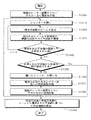
図23は、本発明に係る形状測定方法の好適な一実施例を示すフローチャートである。 FIG. 23 is a flowchart showing a preferred embodiment of the shape measuring method according to the present invention.
図23を参照すると、制御部120は、複数のレーザー装置111,116のいずれか一方のレーザー装置を稼働するために一つのレーザー装置111を選択し、レーザー装置111に電流を印加する(S1300)。
そして、制御部120は、電流の印加されたレーザー装置111から放出されるビームを遮断するシャッター131を開く(S1310)。
制御部120は、稼働したレーザー装置111を通じて特定周波数のビームを放出させる(S1320)。
ここで、制御部120は、稼働したレーザー装置111が生成したビームの波長を検出し、検出された波長に基づいてレーザー装置111に印加される電流を調節し、生成したビームの共鳴周波数が検出されるか否かを確認し、生成したビームの共鳴周波数が検出された場合には、レーザー装置111は、生成したビームを特定周波数のビームとして放出する。光学装置部140は、レーザー装置111から放出されたビームを被検体101に投射させて干渉縞を生成し、撮像部150は、生成された干渉縞を撮像し、撮像された干渉縞を制御部が獲得する(S1330)。
Referring to FIG. 23, the
Then, the
The
Here, the
制御部120は、獲得された干渉縞の個数が予め設定された値と同一か否かを確認する(S1340)。
同一でないと、制御部120は段階S1320に戻る。同一であると、獲得された干渉縞から被検体101の形状情報を算出できるか否かを確認する(S1350)。
算出可能でない場合は、制御部120は、開いたシャッター131を閉じる(S1360)。
そして、制御部120は、稼働したレーザー装置111に印加される電流の供給を中断する(S1370)。
制御部120は、複数のレーザー装置のうちのいずれか他方のレーザー装置116に電流を印加する(S1380)。
そして、制御部120は、段階S1310以降の段階を再び行う。算出可能な場合には、制御部120は、特定周波数と各特定周波数のビームから獲得された干渉縞に基づいて形状情報を算出する(S1390)。
The
If not, the
When the calculation is not possible, the
And the
The
And the
以上では好ましい実施例及び図面に上げて本発明を説明してきたが、本発明は、上記特定の実施例に限定されず、特許請求の範囲で請求する本発明の要旨を逸脱しない限度内で、本発明の属する技術分野における通常の知識を有する者にとっては様々な変形実施が可能であり、それらの変更はいずれも特許請求の範囲に含まれる。 Although the present invention has been described with reference to the preferred embodiments and drawings, the present invention is not limited to the specific embodiments described above, and is within the scope not departing from the gist of the present invention claimed in the claims. Various modifications may be made by those having ordinary knowledge in the technical field to which the present invention pertains, and all such modifications are within the scope of the claims.
本発明に係る形状測定装置及びその方法によれば、安定した周波数を放出する複数個の多チャネル周波数スキャニングレーザー装置を用いて光を放出するため、高さの大きい被検体の形状を正確で精密に測定することができる。
また、本発明による形状測定装置及びその方法は、基準面の位置移動を要求せず、これにより、基準面の位置移動による時間所要及び誤差発生を防止し、被検体の形状を迅速で正確に測定することができる。
According to the shape measuring apparatus and method therefor according to the present invention, light is emitted using a plurality of multi-channel frequency scanning laser devices that emit stable frequencies, so that the shape of a subject having a large height can be accurately and precisely measured. Can be measured.
In addition, the shape measuring apparatus and method according to the present invention do not require the position movement of the reference plane, thereby preventing the time requirement and the error due to the position movement of the reference plane, and the shape of the subject can be quickly and accurately. Can be measured.
Claims (18)
前記出力された干渉信号から、前記生成されたビームの波長を検出し、該検出された波長に基づいて複数の前記レーザー装置を制御する制御部と、
を含むことを特徴とする、形状測定装置。 A plurality of laser devices that generate a beam, emit a beam of a specific frequency among the generated beams, and output an interference signal for detecting a wavelength of the generated beam;
A controller that detects a wavelength of the generated beam from the output interference signal and controls the plurality of laser devices based on the detected wavelength;
A shape measuring device comprising:
前記ビームを生成する半導体レーザーと、
前記生成されたビームの波長を検出するための干渉信号を生成して出力する干渉信号生成部と、
前記特定周波数を共振周波数として有し、前記生成されたビームが照射され、該照射されたビームの周波数と前記共振周波数とが同一の場合には、前記照射されたビームを前記半導体レーザーにフィードバックする外部反射体と、
前記外部反射体が前記照射されたビームをフィードバックした場合には、前記生成されたビームを外部に放出する光伝達部と、
を含むことを特徴とする、請求項1に記載の形状測定装置。 The laser device is
A semiconductor laser for generating the beam;
An interference signal generator for generating and outputting an interference signal for detecting the wavelength of the generated beam;
When the generated beam is irradiated with the specific frequency as a resonance frequency, and the frequency of the irradiated beam is the same as the resonance frequency, the irradiated beam is fed back to the semiconductor laser. An external reflector,
When the external reflector feeds back the irradiated beam, a light transmission unit that emits the generated beam to the outside;
The shape measuring device according to claim 1, comprising:
開閉され、閉じた場合には、前記放出されたビームが前記光学装置部に照射されるのを遮断する複数のシャッターと、
前記生成された干渉縞を撮像する撮像部と、
をさらに含むことを特徴とする、請求項1に記載の形状測定装置。 An optical device that projects the emitted beam onto the surface of the subject to generate interference fringes of the subject;
A plurality of shutters for blocking the emitted beam from being applied to the optical device unit when opened and closed and closed;
An imaging unit for imaging the generated interference fringes;
The shape measuring device according to claim 1, further comprising:
前記複数のレーザー装置のうちいずれか一方のレーザー装置を稼働する第1稼働段階と、
前記稼働したレーザー装置から複数の特定周波数のビームをそれぞれ放出させ、前記放出された特定周波数のビームのそれぞれを被検体に投射させて、前記特定周波数のそれぞれに対する前記被検体の干渉縞を獲得する干渉縞獲得段階と、
前記稼働したレーザー装置を停止させ、複数のレーザー装置のうちいずれか他方のレーザー装置を稼働する第2稼働段階と、
含むことを特徴とする、形状測定方法。 A method of measuring a shape using a plurality of laser devices,
A first operation stage of operating any one of the plurality of laser devices;
A plurality of specific frequency beams are emitted from the activated laser device, and each of the emitted specific frequency beams is projected onto a subject to obtain interference fringes of the subject for each of the specific frequencies. An interference fringe acquisition stage;
A second operation stage of stopping the activated laser device and operating one of the plurality of laser devices;
A shape measuring method, comprising:
前記複数のレーザー装置のうちいずれか一方のレーザー装置に電流を印加する段階と、
前記電流が印加されたレーザー装置から放出されるビームを遮断するシャッターを開く段階と、
を含むことを特徴とする、請求項11に記載の形状測定方法。 The first operation stage includes
Applying a current to any one of the plurality of laser devices;
Opening a shutter that blocks a beam emitted from the laser device to which the current is applied;
The shape measuring method according to claim 11, comprising:
前記稼働したレーザー装置を通じて特定周波数のビームを放出するビーム放出段階と、
前記放出されたビームを被検体の表面に投射させて、前記被検体の干渉縞を獲得する段階と、
を含むことを特徴とする、請求項11に記載の形状測定方法。 The interference fringe acquisition step includes
A beam emitting step of emitting a beam of a specific frequency through the activated laser device;
Projecting the emitted beam onto the surface of the subject to obtain interference fringes of the subject;
The shape measuring method according to claim 11, comprising:
前記稼働したレーザー装置で生成されたビームの波長を検出する段階と、
前記検出された波長に基づいて、前記レーザー装置に印加される電流を調節する段階と、
前記ビームの共鳴周波数を検出する段階と、
前記ビームの共鳴周波数が検出された場合には、前記ビームを前記特定周波数のビームとして放出する段階と、
を含むことを特徴とする、請求項13に記載の形状測定方法; The beam emitting step comprises:
Detecting the wavelength of the beam generated by the activated laser device;
Adjusting the current applied to the laser device based on the detected wavelength;
Detecting a resonance frequency of the beam;
If the resonance frequency of the beam is detected, emitting the beam as a beam of the specific frequency;
The shape measuring method according to claim 13, characterized by comprising:
前記稼働したレーザー装置から放出されるビームを遮断するシャッターを閉じる段階と、
前記稼働したレーザー装置に印加される電流の供給を中断する段階と、
前記複数のレーザー装置のうちいずれか他方のレーザー装置に電流を印加する段階と、
前記電流の印加されたレーザー装置から放出されるビームを遮断するシャッターを開く段階と、
を含むことを特徴とする、請求項11に記載の形状測定方法。 The second operation stage includes
Closing a shutter that blocks a beam emitted from the activated laser device;
Interrupting the supply of current applied to the activated laser device;
Applying a current to the other laser device of the plurality of laser devices;
Opening a shutter that blocks a beam emitted from the laser device to which the current is applied;
The shape measuring method according to claim 11, comprising:
前記ビームを生成する半導体レーザーと、
前記生成されたビームの波長を検出するための干渉信号を生成して出力する干渉信号生成部と、
前記特定周波数を共振周波数として有し、前記生成されたビームが照射され、該照射されたビームの周波数と前記共振周波数とが同一の場合には、前記照射されたビームを前記半導体レーザーにフィードバックする外部反射体と、
前記外部反射体が前記照射されたビームをフィードバックした場合には、前記生成されたビームを外部に放出する光伝達部と、
を含むことを特徴とする、請求項11に記載の形状測定方法。 The laser device is
A semiconductor laser for generating the beam;
An interference signal generator for generating and outputting an interference signal for detecting the wavelength of the generated beam;
When the generated beam is irradiated with the specific frequency as a resonance frequency, and the frequency of the irradiated beam is the same as the resonance frequency, the irradiated beam is fed back to the semiconductor laser. An external reflector,
When the external reflector feeds back the irradiated beam, a light transmission unit that emits the generated beam to the outside;
The shape measuring method according to claim 11, comprising:
Applications Claiming Priority (2)
| Application Number | Priority Date | Filing Date | Title |
|---|---|---|---|
| KR1020070091213A KR100925783B1 (en) | 2007-09-07 | 2007-09-07 | Apparatus and method for measuring shape |
| PCT/KR2008/004810 WO2009031770A1 (en) | 2007-09-07 | 2008-08-19 | Shape measurement apparatus and method |
Publications (2)
| Publication Number | Publication Date |
|---|---|
| JP2011511928A true JP2011511928A (en) | 2011-04-14 |
| JP2011511928A5 JP2011511928A5 (en) | 2011-05-26 |
Family
ID=40429055
Family Applications (1)
| Application Number | Title | Priority Date | Filing Date |
|---|---|---|---|
| JP2010523935A Pending JP2011511928A (en) | 2007-09-07 | 2008-08-19 | Shape measuring apparatus and method |
Country Status (4)
| Country | Link |
|---|---|
| US (1) | US8279448B2 (en) |
| JP (1) | JP2011511928A (en) |
| KR (1) | KR100925783B1 (en) |
| WO (1) | WO2009031770A1 (en) |
Families Citing this family (4)
| Publication number | Priority date | Publication date | Assignee | Title |
|---|---|---|---|---|
| CN105890538A (en) * | 2014-12-30 | 2016-08-24 | 广东工业大学 | Three-surface interference type high-accuracy curved surface profile measuring system and method |
| CN105371777B (en) * | 2015-10-29 | 2018-03-09 | 北京交通大学 | The method and system of measurement deformation of body in real time |
| EP3621293B1 (en) * | 2018-04-28 | 2022-02-09 | Guangdong Oppo Mobile Telecommunications Corp., Ltd. | Image processing method, apparatus and computer-readable storage medium |
| US11846574B2 (en) | 2020-10-29 | 2023-12-19 | Hand Held Products, Inc. | Apparatuses, systems, and methods for sample capture and extraction |
Citations (9)
| Publication number | Priority date | Publication date | Assignee | Title |
|---|---|---|---|---|
| JPS63311104A (en) * | 1987-06-15 | 1988-12-19 | Olympus Optical Co Ltd | Semiconductor laser interferometer |
| JPH039202A (en) * | 1989-06-07 | 1991-01-17 | Canon Inc | Semiconductor laser length measuring instrument |
| JPH04297807A (en) * | 1991-03-27 | 1992-10-21 | Mitsutoyo Corp | Phase shift micro fizeau interferometer |
| JPH07306006A (en) * | 1994-05-12 | 1995-11-21 | Asahi Optical Co Ltd | Method for detecting phase in semiconductor laser phase shift interferometer |
| JPH10215027A (en) * | 1997-01-29 | 1998-08-11 | Mitsubishi Heavy Ind Ltd | Method and apparatus for optical-frequency variable operation |
| JPH11218411A (en) * | 1998-02-02 | 1999-08-10 | Fuji Xerox Co Ltd | Measurement method for interference and measurement device of interference |
| JP2001059714A (en) * | 1999-08-20 | 2001-03-06 | Inst Of Physical & Chemical Res | Shape measuring method and device |
| JP2002214049A (en) * | 2001-01-17 | 2002-07-31 | Ando Electric Co Ltd | Wavelength monitor |
| JP2006266841A (en) * | 2005-03-23 | 2006-10-05 | National Institute Of Advanced Industrial & Technology | Method for measuring shape and step through interference fringes |
Family Cites Families (6)
| Publication number | Priority date | Publication date | Assignee | Title |
|---|---|---|---|---|
| US4907237A (en) * | 1988-10-18 | 1990-03-06 | The United States Of America As Represented By The Secretary Of Commerce | Optical feedback locking of semiconductor lasers |
| US5077748A (en) * | 1991-04-01 | 1991-12-31 | International Business Machines Corporation | Laser system and method |
| JPH05206561A (en) * | 1992-01-27 | 1993-08-13 | Nippon Telegr & Teleph Corp <Ntt> | Light feedback type light frequency offset locking device |
| JP3421309B2 (en) * | 2000-09-01 | 2003-06-30 | 日本電信電話株式会社 | Surface shape measuring method and surface shape measuring instrument |
| US6717679B2 (en) * | 2001-11-15 | 2004-04-06 | Zygo Corporation | Dispersive null-optics for aspheric surface and wavefront metrology |
| US6882666B2 (en) | 2002-10-22 | 2005-04-19 | Inplane Photonics, Inc. | Kink free operation of pump lasers having diffraction grating for providing wavelength stabilization |
-
2007
- 2007-09-07 KR KR1020070091213A patent/KR100925783B1/en active IP Right Grant
-
2008
- 2008-08-19 US US12/676,245 patent/US8279448B2/en not_active Expired - Fee Related
- 2008-08-19 WO PCT/KR2008/004810 patent/WO2009031770A1/en active Application Filing
- 2008-08-19 JP JP2010523935A patent/JP2011511928A/en active Pending
Patent Citations (9)
| Publication number | Priority date | Publication date | Assignee | Title |
|---|---|---|---|---|
| JPS63311104A (en) * | 1987-06-15 | 1988-12-19 | Olympus Optical Co Ltd | Semiconductor laser interferometer |
| JPH039202A (en) * | 1989-06-07 | 1991-01-17 | Canon Inc | Semiconductor laser length measuring instrument |
| JPH04297807A (en) * | 1991-03-27 | 1992-10-21 | Mitsutoyo Corp | Phase shift micro fizeau interferometer |
| JPH07306006A (en) * | 1994-05-12 | 1995-11-21 | Asahi Optical Co Ltd | Method for detecting phase in semiconductor laser phase shift interferometer |
| JPH10215027A (en) * | 1997-01-29 | 1998-08-11 | Mitsubishi Heavy Ind Ltd | Method and apparatus for optical-frequency variable operation |
| JPH11218411A (en) * | 1998-02-02 | 1999-08-10 | Fuji Xerox Co Ltd | Measurement method for interference and measurement device of interference |
| JP2001059714A (en) * | 1999-08-20 | 2001-03-06 | Inst Of Physical & Chemical Res | Shape measuring method and device |
| JP2002214049A (en) * | 2001-01-17 | 2002-07-31 | Ando Electric Co Ltd | Wavelength monitor |
| JP2006266841A (en) * | 2005-03-23 | 2006-10-05 | National Institute Of Advanced Industrial & Technology | Method for measuring shape and step through interference fringes |
Also Published As
| Publication number | Publication date |
|---|---|
| US20100182614A1 (en) | 2010-07-22 |
| KR100925783B1 (en) | 2009-11-11 |
| US8279448B2 (en) | 2012-10-02 |
| KR20090025971A (en) | 2009-03-11 |
| WO2009031770A1 (en) | 2009-03-12 |
Similar Documents
| Publication | Publication Date | Title |
|---|---|---|
| JP5149486B2 (en) | Interferometer, shape measurement method | |
| US9910255B2 (en) | Optical system for generating a pattern which changes over time for a confocal microscope | |
| US6992779B2 (en) | Interferometer apparatus for both low and high coherence measurement and method thereof | |
| US9372068B2 (en) | Measuring apparatus including multi-wavelength interferometer | |
| US20110304854A1 (en) | Instantaneous, phase measuring interferometer apparatus and method | |
| KR20090116731A (en) | Method and device for monitoring multiple mirror arrays in an illumination system of a microlithographic projection exposure apparatus | |
| TW201822704A (en) | Systems and methods for optimizing focus for imaging-based overlay metrology | |
| TW201825864A (en) | A scanning white-light interferometry system for characterization of patterned semiconductor features | |
| JP2011511928A (en) | Shape measuring apparatus and method | |
| KR101527764B1 (en) | 3 dimension image measuring apparatus using a laser interferometer | |
| JP4880519B2 (en) | Interference measurement device | |
| KR100941981B1 (en) | Laser interferometric mekometer | |
| US20150354953A1 (en) | Laser triangulation sensor and method of measurement with laser triangulation sensor | |
| JP5421677B2 (en) | Displacement measuring device using optical interferometer | |
| JP2003294418A (en) | Evaluation apparatus and evaluation method for minute cycle structure | |
| JP2004069585A (en) | Method for measuring parallelism | |
| JP5480479B2 (en) | Shape measuring device and calibration method of shape measuring device | |
| JP2009069075A (en) | Oblique incidence interferometer and method for calibrating the same | |
| US20140268173A1 (en) | Shape measurement apparatus, measurement method, and method of manufacturing article | |
| JP3964260B2 (en) | Shape measuring device | |
| US20210333148A1 (en) | Measurement apparatus and measurement method | |
| JP7451704B2 (en) | Fast phase shift interferometry using laser frequency shift | |
| US20210377511A1 (en) | Ultrafast camera system and measurement method thereof | |
| JP5376284B2 (en) | Interferometry method and interferometer | |
| JP2004077223A (en) | Optical heterodyne interferometer |
Legal Events
| Date | Code | Title | Description |
|---|---|---|---|
| A977 | Report on retrieval |
Free format text: JAPANESE INTERMEDIATE CODE: A971007 Effective date: 20111116 |
|
| A131 | Notification of reasons for refusal |
Free format text: JAPANESE INTERMEDIATE CODE: A131 Effective date: 20111122 |
|
| A521 | Written amendment |
Free format text: JAPANESE INTERMEDIATE CODE: A523 Effective date: 20120215 |
|
| A02 | Decision of refusal |
Free format text: JAPANESE INTERMEDIATE CODE: A02 Effective date: 20121211 |