JP2011503882A - Particle beam assisted modification of thin film materials - Google Patents
Particle beam assisted modification of thin film materials Download PDFInfo
- Publication number
- JP2011503882A JP2011503882A JP2010533345A JP2010533345A JP2011503882A JP 2011503882 A JP2011503882 A JP 2011503882A JP 2010533345 A JP2010533345 A JP 2010533345A JP 2010533345 A JP2010533345 A JP 2010533345A JP 2011503882 A JP2011503882 A JP 2011503882A
- Authority
- JP
- Japan
- Prior art keywords
- region
- particles
- substrate
- particle
- extending
- Prior art date
- Legal status (The legal status is an assumption and is not a legal conclusion. Google has not performed a legal analysis and makes no representation as to the accuracy of the status listed.)
- Withdrawn
Links
- 239000002245 particle Substances 0.000 title claims abstract description 163
- 239000000463 material Substances 0.000 title claims description 23
- 239000010409 thin film Substances 0.000 title description 15
- 230000004048 modification Effects 0.000 title description 6
- 238000012986 modification Methods 0.000 title description 6
- 239000000758 substrate Substances 0.000 claims abstract description 144
- 238000000034 method Methods 0.000 claims abstract description 71
- 239000013078 crystal Substances 0.000 claims abstract description 43
- 239000012071 phase Substances 0.000 claims description 38
- 230000006911 nucleation Effects 0.000 claims description 11
- 238000010899 nucleation Methods 0.000 claims description 11
- 238000000137 annealing Methods 0.000 claims description 10
- 230000008859 change Effects 0.000 claims description 8
- 239000007790 solid phase Substances 0.000 claims description 6
- 230000001965 increasing effect Effects 0.000 claims description 5
- 238000004151 rapid thermal annealing Methods 0.000 claims description 5
- 238000005224 laser annealing Methods 0.000 claims description 3
- 229910052782 aluminium Inorganic materials 0.000 claims description 2
- 229910052799 carbon Inorganic materials 0.000 claims description 2
- 229910052733 gallium Inorganic materials 0.000 claims description 2
- 229910052698 phosphorus Inorganic materials 0.000 claims description 2
- 229910021480 group 4 element Inorganic materials 0.000 claims 4
- 239000002923 metal particle Substances 0.000 claims 2
- 229910052718 tin Inorganic materials 0.000 claims 2
- 229910052769 Ytterbium Inorganic materials 0.000 claims 1
- 229910052787 antimony Inorganic materials 0.000 claims 1
- 229910052786 argon Inorganic materials 0.000 claims 1
- 229910052785 arsenic Inorganic materials 0.000 claims 1
- 229910052797 bismuth Inorganic materials 0.000 claims 1
- 229910052796 boron Inorganic materials 0.000 claims 1
- 150000001793 charged compounds Chemical class 0.000 claims 1
- 230000007423 decrease Effects 0.000 claims 1
- 229910052732 germanium Inorganic materials 0.000 claims 1
- 229910052735 hafnium Inorganic materials 0.000 claims 1
- 229910052734 helium Inorganic materials 0.000 claims 1
- 229910052738 indium Inorganic materials 0.000 claims 1
- 229910052743 krypton Inorganic materials 0.000 claims 1
- 229910052754 neon Inorganic materials 0.000 claims 1
- 229910052763 palladium Inorganic materials 0.000 claims 1
- 229910052697 platinum Inorganic materials 0.000 claims 1
- 229910052704 radon Inorganic materials 0.000 claims 1
- 229910052719 titanium Inorganic materials 0.000 claims 1
- 229910052724 xenon Inorganic materials 0.000 claims 1
- 229910052726 zirconium Inorganic materials 0.000 claims 1
- 238000012545 processing Methods 0.000 abstract description 16
- 239000010410 layer Substances 0.000 description 66
- 239000010408 film Substances 0.000 description 28
- 229910021417 amorphous silicon Inorganic materials 0.000 description 26
- 230000008569 process Effects 0.000 description 26
- 239000011521 glass Substances 0.000 description 17
- 150000002500 ions Chemical class 0.000 description 16
- 238000006243 chemical reaction Methods 0.000 description 14
- 230000007246 mechanism Effects 0.000 description 14
- 229910021419 crystalline silicon Inorganic materials 0.000 description 13
- 238000004519 manufacturing process Methods 0.000 description 11
- 238000002425 crystallisation Methods 0.000 description 10
- 230000008025 crystallization Effects 0.000 description 10
- 238000010586 diagram Methods 0.000 description 7
- 238000000605 extraction Methods 0.000 description 6
- 238000010438 heat treatment Methods 0.000 description 6
- 241000894007 species Species 0.000 description 6
- 230000009466 transformation Effects 0.000 description 6
- 238000004090 dissolution Methods 0.000 description 5
- 230000008018 melting Effects 0.000 description 5
- 238000002844 melting Methods 0.000 description 5
- 229910021420 polycrystalline silicon Inorganic materials 0.000 description 5
- 238000007711 solidification Methods 0.000 description 5
- 230000008023 solidification Effects 0.000 description 5
- 239000002800 charge carrier Substances 0.000 description 4
- 238000001816 cooling Methods 0.000 description 4
- 230000000694 effects Effects 0.000 description 4
- 238000005468 ion implantation Methods 0.000 description 4
- 239000010453 quartz Substances 0.000 description 4
- 239000004065 semiconductor Substances 0.000 description 4
- VYPSYNLAJGMNEJ-UHFFFAOYSA-N silicon dioxide Inorganic materials O=[Si]=O VYPSYNLAJGMNEJ-UHFFFAOYSA-N 0.000 description 4
- 230000001133 acceleration Effects 0.000 description 3
- 230000005591 charge neutralization Effects 0.000 description 3
- 238000002438 flame photometric detection Methods 0.000 description 3
- 239000007789 gas Substances 0.000 description 3
- 238000009413 insulation Methods 0.000 description 3
- 238000010884 ion-beam technique Methods 0.000 description 3
- 239000002184 metal Substances 0.000 description 3
- 229910052751 metal Inorganic materials 0.000 description 3
- 230000005855 radiation Effects 0.000 description 3
- 239000010980 sapphire Substances 0.000 description 3
- 229910052594 sapphire Inorganic materials 0.000 description 3
- 239000007787 solid Substances 0.000 description 3
- 239000002344 surface layer Substances 0.000 description 3
- 230000002123 temporal effect Effects 0.000 description 3
- XUIMIQQOPSSXEZ-UHFFFAOYSA-N Silicon Chemical compound [Si] XUIMIQQOPSSXEZ-UHFFFAOYSA-N 0.000 description 2
- 230000008901 benefit Effects 0.000 description 2
- 239000002178 crystalline material Substances 0.000 description 2
- 238000005137 deposition process Methods 0.000 description 2
- 238000005516 engineering process Methods 0.000 description 2
- 230000008020 evaporation Effects 0.000 description 2
- 238000001704 evaporation Methods 0.000 description 2
- 239000011888 foil Substances 0.000 description 2
- 230000014509 gene expression Effects 0.000 description 2
- 230000009477 glass transition Effects 0.000 description 2
- 239000012212 insulator Substances 0.000 description 2
- 238000004518 low pressure chemical vapour deposition Methods 0.000 description 2
- 229910021421 monocrystalline silicon Inorganic materials 0.000 description 2
- 230000007935 neutral effect Effects 0.000 description 2
- 238000006386 neutralization reaction Methods 0.000 description 2
- 238000000623 plasma-assisted chemical vapour deposition Methods 0.000 description 2
- 239000004033 plastic Substances 0.000 description 2
- 229920003023 plastic Polymers 0.000 description 2
- 229920000139 polyethylene terephthalate Polymers 0.000 description 2
- 239000005020 polyethylene terephthalate Substances 0.000 description 2
- 229910052710 silicon Inorganic materials 0.000 description 2
- 239000010703 silicon Substances 0.000 description 2
- 238000012546 transfer Methods 0.000 description 2
- 230000007704 transition Effects 0.000 description 2
- OKTJSMMVPCPJKN-UHFFFAOYSA-N Carbon Chemical compound [C] OKTJSMMVPCPJKN-UHFFFAOYSA-N 0.000 description 1
- 229910004613 CdTe Inorganic materials 0.000 description 1
- 229910001218 Gallium arsenide Inorganic materials 0.000 description 1
- 229910000530 Gallium indium arsenide Inorganic materials 0.000 description 1
- OAICVXFJPJFONN-UHFFFAOYSA-N Phosphorus Chemical compound [P] OAICVXFJPJFONN-UHFFFAOYSA-N 0.000 description 1
- 240000007320 Pinus strobus Species 0.000 description 1
- 229910000577 Silicon-germanium Inorganic materials 0.000 description 1
- 238000009825 accumulation Methods 0.000 description 1
- 239000013543 active substance Substances 0.000 description 1
- 229910045601 alloy Inorganic materials 0.000 description 1
- 239000000956 alloy Substances 0.000 description 1
- 238000005280 amorphization Methods 0.000 description 1
- 230000004888 barrier function Effects 0.000 description 1
- 230000015572 biosynthetic process Effects 0.000 description 1
- 230000000903 blocking effect Effects 0.000 description 1
- 239000000969 carrier Substances 0.000 description 1
- 239000000919 ceramic Substances 0.000 description 1
- 230000015271 coagulation Effects 0.000 description 1
- 238000005345 coagulation Methods 0.000 description 1
- 238000004891 communication Methods 0.000 description 1
- 150000001875 compounds Chemical class 0.000 description 1
- 239000000356 contaminant Substances 0.000 description 1
- 229910052802 copper Inorganic materials 0.000 description 1
- 230000008878 coupling Effects 0.000 description 1
- 238000010168 coupling process Methods 0.000 description 1
- 238000005859 coupling reaction Methods 0.000 description 1
- 230000009849 deactivation Effects 0.000 description 1
- 230000007547 defect Effects 0.000 description 1
- 230000007812 deficiency Effects 0.000 description 1
- 238000000151 deposition Methods 0.000 description 1
- 230000008021 deposition Effects 0.000 description 1
- 230000001627 detrimental effect Effects 0.000 description 1
- 238000009792 diffusion process Methods 0.000 description 1
- 239000002019 doping agent Substances 0.000 description 1
- 230000005672 electromagnetic field Effects 0.000 description 1
- 239000012530 fluid Substances 0.000 description 1
- 230000004907 flux Effects 0.000 description 1
- 238000005247 gettering Methods 0.000 description 1
- 238000007654 immersion Methods 0.000 description 1
- 238000002513 implantation Methods 0.000 description 1
- 239000012535 impurity Substances 0.000 description 1
- 230000001939 inductive effect Effects 0.000 description 1
- 239000007788 liquid Substances 0.000 description 1
- 238000005259 measurement Methods 0.000 description 1
- 239000000155 melt Substances 0.000 description 1
- 230000005405 multipole Effects 0.000 description 1
- 238000002161 passivation Methods 0.000 description 1
- 230000000149 penetrating effect Effects 0.000 description 1
- 239000011574 phosphorus Substances 0.000 description 1
- -1 polyethylene terephthalate Polymers 0.000 description 1
- 239000003870 refractory metal Substances 0.000 description 1
- 229910052711 selenium Inorganic materials 0.000 description 1
- 230000035939 shock Effects 0.000 description 1
- 239000002210 silicon-based material Substances 0.000 description 1
- 229910052709 silver Inorganic materials 0.000 description 1
- 238000004544 sputter deposition Methods 0.000 description 1
- 229910052717 sulfur Inorganic materials 0.000 description 1
- 238000004781 supercooling Methods 0.000 description 1
- 229910052715 tantalum Inorganic materials 0.000 description 1
- 238000010257 thawing Methods 0.000 description 1
- 229910052721 tungsten Inorganic materials 0.000 description 1
- 238000001429 visible spectrum Methods 0.000 description 1
Images


Classifications
-
- H—ELECTRICITY
- H01—ELECTRIC ELEMENTS
- H01L—SEMICONDUCTOR DEVICES NOT COVERED BY CLASS H10
- H01L21/00—Processes or apparatus adapted for the manufacture or treatment of semiconductor or solid state devices or of parts thereof
- H01L21/02—Manufacture or treatment of semiconductor devices or of parts thereof
- H01L21/02104—Forming layers
- H01L21/02365—Forming inorganic semiconducting materials on a substrate
- H01L21/02656—Special treatments
- H01L21/02664—Aftertreatments
- H01L21/02667—Crystallisation or recrystallisation of non-monocrystalline semiconductor materials, e.g. regrowth
- H01L21/02689—Crystallisation or recrystallisation of non-monocrystalline semiconductor materials, e.g. regrowth using particle beams
-
- C—CHEMISTRY; METALLURGY
- C30—CRYSTAL GROWTH
- C30B—SINGLE-CRYSTAL GROWTH; UNIDIRECTIONAL SOLIDIFICATION OF EUTECTIC MATERIAL OR UNIDIRECTIONAL DEMIXING OF EUTECTOID MATERIAL; REFINING BY ZONE-MELTING OF MATERIAL; PRODUCTION OF A HOMOGENEOUS POLYCRYSTALLINE MATERIAL WITH DEFINED STRUCTURE; SINGLE CRYSTALS OR HOMOGENEOUS POLYCRYSTALLINE MATERIAL WITH DEFINED STRUCTURE; AFTER-TREATMENT OF SINGLE CRYSTALS OR A HOMOGENEOUS POLYCRYSTALLINE MATERIAL WITH DEFINED STRUCTURE; APPARATUS THEREFOR
- C30B1/00—Single-crystal growth directly from the solid state
- C30B1/02—Single-crystal growth directly from the solid state by thermal treatment, e.g. strain annealing
- C30B1/023—Single-crystal growth directly from the solid state by thermal treatment, e.g. strain annealing from solids with amorphous structure
-
- C—CHEMISTRY; METALLURGY
- C30—CRYSTAL GROWTH
- C30B—SINGLE-CRYSTAL GROWTH; UNIDIRECTIONAL SOLIDIFICATION OF EUTECTIC MATERIAL OR UNIDIRECTIONAL DEMIXING OF EUTECTOID MATERIAL; REFINING BY ZONE-MELTING OF MATERIAL; PRODUCTION OF A HOMOGENEOUS POLYCRYSTALLINE MATERIAL WITH DEFINED STRUCTURE; SINGLE CRYSTALS OR HOMOGENEOUS POLYCRYSTALLINE MATERIAL WITH DEFINED STRUCTURE; AFTER-TREATMENT OF SINGLE CRYSTALS OR A HOMOGENEOUS POLYCRYSTALLINE MATERIAL WITH DEFINED STRUCTURE; APPARATUS THEREFOR
- C30B29/00—Single crystals or homogeneous polycrystalline material with defined structure characterised by the material or by their shape
- C30B29/02—Elements
- C30B29/06—Silicon
-
- H—ELECTRICITY
- H01—ELECTRIC ELEMENTS
- H01L—SEMICONDUCTOR DEVICES NOT COVERED BY CLASS H10
- H01L21/00—Processes or apparatus adapted for the manufacture or treatment of semiconductor or solid state devices or of parts thereof
- H01L21/02—Manufacture or treatment of semiconductor devices or of parts thereof
- H01L21/04—Manufacture or treatment of semiconductor devices or of parts thereof the devices having at least one potential-jump barrier or surface barrier, e.g. PN junction, depletion layer or carrier concentration layer
- H01L21/18—Manufacture or treatment of semiconductor devices or of parts thereof the devices having at least one potential-jump barrier or surface barrier, e.g. PN junction, depletion layer or carrier concentration layer the devices having semiconductor bodies comprising elements of Group IV of the Periodic System or AIIIBV compounds with or without impurities, e.g. doping materials
- H01L21/26—Bombardment with radiation
- H01L21/263—Bombardment with radiation with high-energy radiation
- H01L21/268—Bombardment with radiation with high-energy radiation using electromagnetic radiation, e.g. laser radiation
-
- H—ELECTRICITY
- H01—ELECTRIC ELEMENTS
- H01L—SEMICONDUCTOR DEVICES NOT COVERED BY CLASS H10
- H01L31/00—Semiconductor devices sensitive to infrared radiation, light, electromagnetic radiation of shorter wavelength or corpuscular radiation and specially adapted either for the conversion of the energy of such radiation into electrical energy or for the control of electrical energy by such radiation; Processes or apparatus specially adapted for the manufacture or treatment thereof or of parts thereof; Details thereof
- H01L31/04—Semiconductor devices sensitive to infrared radiation, light, electromagnetic radiation of shorter wavelength or corpuscular radiation and specially adapted either for the conversion of the energy of such radiation into electrical energy or for the control of electrical energy by such radiation; Processes or apparatus specially adapted for the manufacture or treatment thereof or of parts thereof; Details thereof adapted as photovoltaic [PV] conversion devices
- H01L31/06—Semiconductor devices sensitive to infrared radiation, light, electromagnetic radiation of shorter wavelength or corpuscular radiation and specially adapted either for the conversion of the energy of such radiation into electrical energy or for the control of electrical energy by such radiation; Processes or apparatus specially adapted for the manufacture or treatment thereof or of parts thereof; Details thereof adapted as photovoltaic [PV] conversion devices characterised by at least one potential-jump barrier or surface barrier
- H01L31/072—Semiconductor devices sensitive to infrared radiation, light, electromagnetic radiation of shorter wavelength or corpuscular radiation and specially adapted either for the conversion of the energy of such radiation into electrical energy or for the control of electrical energy by such radiation; Processes or apparatus specially adapted for the manufacture or treatment thereof or of parts thereof; Details thereof adapted as photovoltaic [PV] conversion devices characterised by at least one potential-jump barrier or surface barrier the potential barriers being only of the PN heterojunction type
- H01L31/0745—Semiconductor devices sensitive to infrared radiation, light, electromagnetic radiation of shorter wavelength or corpuscular radiation and specially adapted either for the conversion of the energy of such radiation into electrical energy or for the control of electrical energy by such radiation; Processes or apparatus specially adapted for the manufacture or treatment thereof or of parts thereof; Details thereof adapted as photovoltaic [PV] conversion devices characterised by at least one potential-jump barrier or surface barrier the potential barriers being only of the PN heterojunction type comprising a AIVBIV heterojunction, e.g. Si/Ge, SiGe/Si or Si/SiC solar cells
- H01L31/0747—Semiconductor devices sensitive to infrared radiation, light, electromagnetic radiation of shorter wavelength or corpuscular radiation and specially adapted either for the conversion of the energy of such radiation into electrical energy or for the control of electrical energy by such radiation; Processes or apparatus specially adapted for the manufacture or treatment thereof or of parts thereof; Details thereof adapted as photovoltaic [PV] conversion devices characterised by at least one potential-jump barrier or surface barrier the potential barriers being only of the PN heterojunction type comprising a AIVBIV heterojunction, e.g. Si/Ge, SiGe/Si or Si/SiC solar cells comprising a heterojunction of crystalline and amorphous materials, e.g. heterojunction with intrinsic thin layer or HIT® solar cells; solar cells
-
- H—ELECTRICITY
- H01—ELECTRIC ELEMENTS
- H01L—SEMICONDUCTOR DEVICES NOT COVERED BY CLASS H10
- H01L31/00—Semiconductor devices sensitive to infrared radiation, light, electromagnetic radiation of shorter wavelength or corpuscular radiation and specially adapted either for the conversion of the energy of such radiation into electrical energy or for the control of electrical energy by such radiation; Processes or apparatus specially adapted for the manufacture or treatment thereof or of parts thereof; Details thereof
- H01L31/18—Processes or apparatus specially adapted for the manufacture or treatment of these devices or of parts thereof
- H01L31/1804—Processes or apparatus specially adapted for the manufacture or treatment of these devices or of parts thereof comprising only elements of Group IV of the Periodic System
- H01L31/182—Special manufacturing methods for polycrystalline Si, e.g. Si ribbon, poly Si ingots, thin films of polycrystalline Si
-
- H—ELECTRICITY
- H01—ELECTRIC ELEMENTS
- H01L—SEMICONDUCTOR DEVICES NOT COVERED BY CLASS H10
- H01L31/00—Semiconductor devices sensitive to infrared radiation, light, electromagnetic radiation of shorter wavelength or corpuscular radiation and specially adapted either for the conversion of the energy of such radiation into electrical energy or for the control of electrical energy by such radiation; Processes or apparatus specially adapted for the manufacture or treatment thereof or of parts thereof; Details thereof
- H01L31/18—Processes or apparatus specially adapted for the manufacture or treatment of these devices or of parts thereof
- H01L31/20—Processes or apparatus specially adapted for the manufacture or treatment of these devices or of parts thereof such devices or parts thereof comprising amorphous semiconductor materials
- H01L31/202—Processes or apparatus specially adapted for the manufacture or treatment of these devices or of parts thereof such devices or parts thereof comprising amorphous semiconductor materials including only elements of Group IV of the Periodic System
-
- H—ELECTRICITY
- H01—ELECTRIC ELEMENTS
- H01L—SEMICONDUCTOR DEVICES NOT COVERED BY CLASS H10
- H01L21/00—Processes or apparatus adapted for the manufacture or treatment of semiconductor or solid state devices or of parts thereof
- H01L21/02—Manufacture or treatment of semiconductor devices or of parts thereof
- H01L21/02104—Forming layers
- H01L21/02365—Forming inorganic semiconducting materials on a substrate
- H01L21/02367—Substrates
- H01L21/0237—Materials
- H01L21/02422—Non-crystalline insulating materials, e.g. glass, polymers
-
- H—ELECTRICITY
- H01—ELECTRIC ELEMENTS
- H01L—SEMICONDUCTOR DEVICES NOT COVERED BY CLASS H10
- H01L21/00—Processes or apparatus adapted for the manufacture or treatment of semiconductor or solid state devices or of parts thereof
- H01L21/02—Manufacture or treatment of semiconductor devices or of parts thereof
- H01L21/02104—Forming layers
- H01L21/02365—Forming inorganic semiconducting materials on a substrate
- H01L21/02518—Deposited layers
- H01L21/02521—Materials
- H01L21/02524—Group 14 semiconducting materials
- H01L21/02532—Silicon, silicon germanium, germanium
-
- Y—GENERAL TAGGING OF NEW TECHNOLOGICAL DEVELOPMENTS; GENERAL TAGGING OF CROSS-SECTIONAL TECHNOLOGIES SPANNING OVER SEVERAL SECTIONS OF THE IPC; TECHNICAL SUBJECTS COVERED BY FORMER USPC CROSS-REFERENCE ART COLLECTIONS [XRACs] AND DIGESTS
- Y02—TECHNOLOGIES OR APPLICATIONS FOR MITIGATION OR ADAPTATION AGAINST CLIMATE CHANGE
- Y02E—REDUCTION OF GREENHOUSE GAS [GHG] EMISSIONS, RELATED TO ENERGY GENERATION, TRANSMISSION OR DISTRIBUTION
- Y02E10/00—Energy generation through renewable energy sources
- Y02E10/50—Photovoltaic [PV] energy
- Y02E10/546—Polycrystalline silicon PV cells
-
- Y—GENERAL TAGGING OF NEW TECHNOLOGICAL DEVELOPMENTS; GENERAL TAGGING OF CROSS-SECTIONAL TECHNOLOGIES SPANNING OVER SEVERAL SECTIONS OF THE IPC; TECHNICAL SUBJECTS COVERED BY FORMER USPC CROSS-REFERENCE ART COLLECTIONS [XRACs] AND DIGESTS
- Y02—TECHNOLOGIES OR APPLICATIONS FOR MITIGATION OR ADAPTATION AGAINST CLIMATE CHANGE
- Y02P—CLIMATE CHANGE MITIGATION TECHNOLOGIES IN THE PRODUCTION OR PROCESSING OF GOODS
- Y02P70/00—Climate change mitigation technologies in the production process for final industrial or consumer products
- Y02P70/50—Manufacturing or production processes characterised by the final manufactured product
Abstract
基板を加工するための方法のいくつかの例を開示する。特定の具体化において、この方法は以下、すなわち、基板の第1の領域に対して、第1の領域において粒界をもつ少なくとも1種の結晶が第2の領域で別の結晶を形成することなく形成されるように、複数の第1の粒子を導入することであり、第2の領域は第1の領域に隣接するもの、および第1の領域において形成された少なくとも1種の結晶の粒界を、複数の第1の粒子の導入の停止後に、第2の領域に延ばすことを含みうる。Several examples of methods for processing a substrate are disclosed. In a particular embodiment, the method includes the following: for the first region of the substrate, at least one crystal having a grain boundary in the first region forms another crystal in the second region A plurality of first particles so that the second region is adjacent to the first region, and at least one crystal grain formed in the first region The field can include extending to the second region after stopping the introduction of the plurality of first particles.
Description
関連出願 この出願は、“薄膜材料の粒子線アシスト修飾”という表題を付け、そして2008年11月12日付けで出願された同時係属の出願番号第12/269327号、および“薄膜材料の粒子線アシスト修飾”という表題を付け、そして2008年11月12日付けで出願された同時係属の出願番号第12/269276号に関する。各々の同時係属出願は、参照することによって全体として組み込む。 RELATED APPLICATIONS This application is entitled “Particle Beam Assist Modification of Thin Film Materials” and co-pending application no. 12/269327, filed November 12, 2008, and “Particle Beams of Thin Film Materials”. It relates to co-pending application no. 12/269276 entitled “Assist Modification” and filed on 12 November 2008. Each copending application is incorporated by reference in its entirety.
分野 本開示は、基材を加工するためのシステムおよび技術に、より一層詳しくは、基材結晶相を形成するためのシステムおよび技術に関する。 FIELD The present disclosure relates to systems and techniques for processing substrates, and more particularly to systems and techniques for forming substrate crystalline phases.
背景 フラットパネルディスプレー(FPD)および太陽電池のような未来技術の広範囲にわたり採用されることは、低コスト基材(基板、サブストレート)上で電気デバイスを製造する能力に依存する。FPDの製造において、典型的に低コストのフラットパネルディスプレー(FPD)のピクセル(画素)は、不活性な、ガラスの基材上で堆積されるアモルファス(非晶質、不定形)シリコンの薄い(-50nm厚さ)フィルム上で典型的に製造されうる薄膜トランジスタ(TFT)によって転換される。しかし、改善されたFPDsはピクセルTFTsがより一層良好に実行されることを必要とし、そしてパネル上へ直接高性能制御電子機器(回路)を製造することは有利である場合がある。1種の利点は、パネルおよび外部制御回路間の高価な、そして潜在的に信頼できない接続のための必要性を排除することにある場合がある。 Background The widespread adoption of future technologies such as flat panel displays (FPD) and solar cells depends on the ability to manufacture electrical devices on low cost substrates (substrates, substrates). In FPD manufacturing, typically low-cost flat panel display (FPD) pixels are thin, amorphous (amorphous) silicon deposited on an inert, glass substrate ( -50 nm thickness) converted by thin film transistors (TFT) that can typically be produced on film. However, improved FPDs require pixel TFTs to perform better and it may be advantageous to manufacture high performance control electronics (circuitry) directly on the panel. One advantage may be to eliminate the need for expensive and potentially unreliable connections between the panel and external control circuitry.
目下のFPDsは、Siの層を含み、それは、低温堆積プロセス、たとえば、スパッタリング、蒸着(蒸発)、プラズマ化学気相成長法(PECVD)、または低圧化学気相堆積(LPCVD)プロセスのようなものを介してディスプレイのガラスパネル上に堆積される。そのような低温プロセスは望ましく、FPDを製造するのに用いるパネルがアモルファスである傾向があり、そしておよそ600℃のガラス転移温度をもつからである。600℃を超えて製造されるならば、パネルは不均一な、または平らでない構造または表面をもつかもしれない。石英(クォーツ)またはサファイヤパネルのようなより一層高い温度耐性ガラスパネルが存在する場合、しかし、そのようなガラスの高いコストは、それらの使用をはばむ。より一層のコスト削減は、より一層安価な、より一層低い温度耐性ガラスまたはプラスチックパネルを用いることができるならば可能であろう。 Current FPDs include layers of Si, such as low temperature deposition processes, such as sputtering, evaporation (evaporation), plasma enhanced chemical vapor deposition (PECVD), or low pressure chemical vapor deposition (LPCVD) processes Deposited on the glass panel of the display. Such a low temperature process is desirable because the panels used to manufacture the FPD tend to be amorphous and have a glass transition temperature of approximately 600 ° C. If manufactured above 600 ° C., the panel may have a non-uniform or uneven structure or surface. Where even higher temperature resistant glass panels such as quartz (quartz) or sapphire panels exist, however, the high cost of such glasses precludes their use. Further cost savings would be possible if even less expensive, lower temperature resistant glass or plastic panels could be used.
低温堆積プロセスは、しかし、最適なSi膜を産生しない。この技術で知られているように、固体Siは3つの普通の相をもち、すなわち、アモルファス、多結晶(poly-crystalline)、および単結晶の相である。Siが低温で堆積する場合、堆積されたSiフィルムはアモルファス相にある傾向をもつ。アモルファスSiフィルムに基づく薄膜トランジスタのチャネルは、多結晶Siまたは単結晶Siのフィルムのいずれかに関してそれらと比較して低い可動性をもつかもしれない。 Low temperature deposition processes, however, do not produce optimal Si films. As is known in the art, solid Si has three common phases: an amorphous, poly-crystalline, and single crystal phase. When Si is deposited at low temperatures, the deposited Si film tends to be in an amorphous phase. Thin film transistor channels based on amorphous Si films may have low mobility compared to them for either polycrystalline Si or single crystal Si films.
多結晶または単結晶のSi層を得るために、パネルは、アモルファスSiフィルムが多結晶または単結晶のフィルムのいずれかに転換されるように、さらなるプロセスを経るかもしれない。多結晶Siフィルムを伴うパネルを得るために、パネルはエキシマーレーザーアニーリング(ELA)プロセスを受けるかもしない。ELAプロセスの例は、米国特許第5,766,989号明細書に更に詳細に見出すことができる。より一層大きな結晶を伴うパネルを得るために、パネルは逐次的横方向結晶化(Sequential Lateral Solidification)(“SLS”)プロセスとして知られるプロセスを受けることがある。SLSプロセスの例は、米国特許第6,322,625号明細書で見出すことができる。ELAおよびSLSプロセスは単結晶または多結晶のSi薄膜を伴うパネルをもたらす場合があるが、各プロセスは不利なしではない。たとえば、双方のプロセスで用いられるエキシマーレーザーは、操作するのに高価である場合があり、高価なTFTになる。そのうえ、負荷サイクルは、結晶質のSiへのアモルファスSiの最良の転換のために最適でないことがある。さらに、エキシマーレーザーは、プロセスの均一性に影響を及ぼすかもしれない送られた力における、パルス対パルスの変動(pulse-to-pulse variation)および空間的不均一性をもつかもしれない。たとえば、ビームの自己干渉によって引き起こされることがあるパルス内不均一性もあるかもしれない。そのようなパルス間およびパルス内不均一性は、不均一な結晶を伴うSiフィルムをもたらすことがある。 In order to obtain a polycrystalline or monocrystalline Si layer, the panel may undergo further processing such that the amorphous Si film is converted to either a polycrystalline or monocrystalline film. In order to obtain a panel with polycrystalline Si film, the panel may undergo an excimer laser annealing (ELA) process. An example of the ELA process can be found in more detail in US Pat. No. 5,766,989. To obtain a panel with even larger crystals, the panel may undergo a process known as a sequential lateral solidification (“SLS”) process. An example of an SLS process can be found in US Pat. No. 6,322,625. Although ELA and SLS processes may result in panels with single or polycrystalline Si thin films, each process is not without disadvantages. For example, excimer lasers used in both processes may be expensive to operate, resulting in expensive TFTs. Moreover, the duty cycle may not be optimal for the best conversion of amorphous Si to crystalline Si. In addition, excimer lasers may have pulse-to-pulse variations and spatial non-uniformities in the transmitted force that may affect process uniformity. There may also be intra-pulse inhomogeneities that may be caused, for example, by beam self-interference. Such inter-pulse and intra-pulse inhomogeneities can result in Si films with non-uniform crystals.
それ自体、低温基材上の高品質結晶質の物質のコスト効果があり、および生産に値する製造のための粒子処理(加工)用の新しい方法および装置が必要である。 As such, there is a need for new methods and apparatus for particle processing (processing) for manufacturing that are cost effective and worthy of production of high quality crystalline materials on low temperature substrates.
概略 基材を加工するための方法のいくつかの例を明らかにする。特定の具体化において、方法は以下の、基材の第1の領域に対して、第1の領域において粒界をもつ少なくとも1種の結晶が第2の領域で別の結晶を形成することなく形成されるように、複数の第1の粒子を導入することであり、第2の領域は第1の領域に隣接するもの、および第1の領域において形成された少なくとも1種の結晶の粒界を、複数の第1の粒子の導入の停止後に、第2の領域に延ばすことを含みうる。 Overview Several examples of methods for processing a substrate are clarified. In a specific embodiment, the method is as follows, with respect to the first region of the substrate, without at least one crystal having a grain boundary in the first region forming another crystal in the second region: A plurality of first grains to be formed, wherein the second region is adjacent to the first region, and at least one crystal grain boundary formed in the first region Extending to the second region after stopping the introduction of the plurality of first particles.
本開示を次に、添付の図面で示すように、その模範的な具体化に関してさらに詳細に説明する。本開示を以下に模範的な具体化を参照して説明するが、本開示がそれに制限されないことを理解すべきである。本明細書での教示にアクセスするこの技術における通常の知識の者は、追加の実現例、修飾、および具体化、ならびに他の使用の分野を認め、それはここに説明するように本開示の範囲内であり、そしてそれに関し、本開示は著しく有用であることができる。 The present disclosure will now be described in more detail with respect to exemplary embodiments thereof as shown in the accompanying drawings. While the present disclosure is described below with reference to exemplary embodiments, it should be understood that the present disclosure is not limited thereto. Those of ordinary skill in the art having access to the teachings herein will recognize additional implementations, modifications, and implementations, as well as other areas of use that are within the scope of this disclosure as described herein. And in this regard, the present disclosure can be significantly useful.
本開示のより一層十分な理解を促すために、次に添付の図面を参照し、そこでは類似の特長は類似の数字に関連する。これらの図は本開示を制限するものとして解釈されてはならず、模範的であることだけを意図する。
詳しい説明 上記に識別され、そして既存のレーザーを基にした薄膜材料処理の他の欠陥を克服するために、粒子を基にした処理のいくつか(5、6くらい)の具体化を明らかにする。粒子を基にした処理は有利である場合があり、それはそれが非平衡性プロセスを促進するかもしれないからである。そのうえ、粒子パラメーターは、レーザーのパラメーターよりも大いに高い精度でコントロールすることができる。粒子パラメーターの例には、空間的パラメーター(たとえば、ビームサイズおよび電流密度)、粒子束(および/またはビーム流)、粒子種、および粒子用量、その他が含まれる。 Detailed Description Reveals some embodiments of particle-based processing (around 5-6) to overcome other deficiencies in the above identified and existing laser-based thin film material processing . Particle-based processing may be advantageous because it may facilitate non-equilibrium processes. Moreover, particle parameters can be controlled with much higher accuracy than laser parameters. Examples of particle parameters include spatial parameters (eg, beam size and current density), particle flux (and / or beam flow), particle type, and particle dose, etc.
本開示において、いくつかの具体化を、文脈において、ビームラインイオン注入システムおよびプラズマを基にした基材処理システム、たとえば、プラズマアシスト(援助された)ドーピング(PLAD)システムまたはプラズマイマージョン(浸入)イオン注入(PIII)システムのようなものに対して明らかにする。しかし、この技術の通常の知識を有する者は、本開示が他のタイプの粒子を基にしたシステムを含む他のシステムに等しく適用できる場合があると認めるべきである。ここで用いる用語“粒子”は、サブ原子の(sub-atomic)、原子の、または分子粒子の、荷電した、または中性のものに言及することができる。たとえば、粒子は、陽子、イオン、原子、または分子、またはガスのクラスターであることができる。 In the present disclosure, some embodiments, in the context, include a beamline ion implantation system and a plasma-based substrate processing system, such as a plasma assisted doping (PLAD) system or a plasma immersion. Clarify for things like ion implantation (PIII) systems. However, one having ordinary skill in the art should appreciate that the present disclosure may be equally applicable to other systems, including other types of particle-based systems. As used herein, the term “particle” can refer to a sub-atomic, atomic, or molecular particle, charged or neutral. For example, the particles can be protons, ions, atoms, or molecules, or clusters of gases.
本開示において、いくつかの具体化は、文脈において基材に対して説明する。基材は、ウエハー(例は、Siウエハー)または複数のフィルムを含む基材であることができる。そのうえ、基材は、1種の元素(例は、Siウエハーまたは金属箔)だけを含有する基本的な基材(elemental substrate)、1よりも多くの元素を含有する合成基材(例は、SiGe、SiC、InTe、GaAs、InP、GaInAs、GaInP;CdTe;CdS、そして(Cu、Agおよび/またはAu)と(Al、Ga、および/またはIn)および(S、Seおよび/またはTe)との組合せで、たとえば、CuInGaSe、CuInSe2のようなもの、他のグループIII-V半導体および他のグループII-VI化合物)、および/または合金基材でありうる。基材に含まれる物質は、金属、半導体、および/または絶縁体(例は、ガラス、ポリエチレンテレフタラート(PET)、サファイヤ、および石英)であることができる。さらに、基材は、複数の層(例は、SOI)を含有する薄膜基材であってよい。基材が複数の層を含む場合、層のうちの少なくとも1種は半導体性フィルムまたは金属性フィルムであってよいが、フィルムの別の1種は絶縁体であることができる。半導体または金属性のフィルムは、単一の絶縁フィルム上に配置することができ、あるいはまた、複数の絶縁フィルムの間に介在させることができる。逆に言えば、絶縁フィルムは、単一の半導体または金属性フィルム上に配置されることができ、または代わりに複数の半導体性または金属性フィルムまたは双方の間に介在させることができる。
相転換
In the present disclosure, some embodiments are described in the context of a substrate. The substrate can be a wafer (eg, a Si wafer) or a substrate comprising a plurality of films. In addition, the substrate can be a basic substrate containing only one element (eg, a Si wafer or a metal foil), a synthetic substrate containing more than one element (eg, SiGe, SiC, InTe, GaAs, InP, GaInAs, GaInP; CdTe; CdS, and (Cu, Ag and / or Au) and (Al, Ga and / or In) and (S, Se and / or Te) In combination, such as CuInGaSe, CuInSe2, other group III-V semiconductors and other group II-VI compounds), and / or alloy substrates. The material included in the substrate can be a metal, a semiconductor, and / or an insulator (eg, glass, polyethylene terephthalate (PET), sapphire, and quartz). Further, the substrate may be a thin film substrate containing a plurality of layers (eg, SOI). When the substrate includes a plurality of layers, at least one of the layers may be a semiconducting film or a metallic film, but another one of the films can be an insulator. The semiconductor or metallic film can be disposed on a single insulating film, or alternatively can be interposed between multiple insulating films. Conversely, the insulating film can be disposed on a single semiconductor or metallic film, or alternatively can be interposed between multiple semiconducting or metallic films or both.
Phase change
薄いアモルファス層の結晶化のための最も迅速なメカニズムは、固相エピタキシャル再成長(SPER)である。SPERでは、アモルファスSiは、下にある、前から存在する、広範囲に及ぶ結晶層を延ばすことによって、結晶質のSiに変換することができる。このシナリオは、結晶Siウエハーの表面層のアニーリングの間、それがイオン注入によってアモルファス化(非晶質化)された後、一般的に遭遇する。本開示は、、アモルファス基材を加工することに関し、そこでは、前から存在する格子が広範囲に存在せず、そして相転換が結晶の成長に先立った結晶の核形成を介して起こる。図1を参照して、広範囲な前から存在する格子を伴わない物質が結晶相にアモルファス相から転換しうる種々のメカニズムのブロック図を示す。この技術で知られるように、結晶相は多結晶相または単結晶相に分類されうる。多結晶相は、時々さらに、結晶のサイズに応じて、異なるカテゴリー(たとえば、マルチ-、マイクロ-、ナノ-結晶質、その他)にさらに再分割されうる。しかし、そのような区別はこの開示の前後関係で重要でない場合があり、図1を説明するのに必要でなくてよい。したがって、これらの相は、結晶相として集合的にここに参照することができる。 The most rapid mechanism for crystallization of thin amorphous layers is solid phase epitaxial regrowth (SPER). In SPER, amorphous Si can be converted to crystalline Si by extending the underlying, preexisting, extensive crystal layer. This scenario is commonly encountered during annealing of the surface layer of a crystalline Si wafer after it has been amorphized (amorphized) by ion implantation. The present disclosure relates to processing amorphous substrates, where the preexisting lattice does not exist extensively and phase transformation occurs through crystal nucleation prior to crystal growth. Referring to FIG. 1, a block diagram of various mechanisms by which a wide range of pre-existing lattice-free materials can be converted from an amorphous phase to a crystalline phase is shown. As is known in the art, the crystalline phase can be classified as a polycrystalline phase or a single crystalline phase. The polycrystalline phase can sometimes be further subdivided into different categories (eg, multi-, micro-, nano-crystalline, etc.) depending on the size of the crystal. However, such a distinction may not be important in the context of this disclosure and may not be necessary to describe FIG. Thus, these phases can be collectively referred to herein as crystalline phases.
図1に例証するように、アモルファス相から結晶相への相転換は種々のメカニズムを介して起こる場合がある。たとえば、転換は溶解および固化(凝結)メカニズム100aおよび固相結晶化(SPC)転換メカニズム100bを介して起こる場合がある。溶解および固化メカニズム100aおよびSPCメカニズムでは、転換は結晶の核形成および結晶の成長を介して起こる場合がある。SPERメカニズムでは、転換は広範囲な前に存在する結晶格子の上での成長によって起こる場合がある。
As illustrated in FIG. 1, the phase transformation from the amorphous phase to the crystalline phase may occur via various mechanisms. For example, the conversion may occur via a dissolution and solidification (coagulation)
溶解および固化のメカニズム100aにおいて、放射の形態のエネルギー、熱、または機械的エネルギーは、アモルファス基材の1部分に導入することができ、およびその部分を溶かすかもしれない。溶解した領域の条件が核形成を誘導するのに十分である場合(たとえば、過冷却)、古典的な核形成論によって説明されるように、結晶は核になることがある。結晶は、2つのスキームを通して核になることができる。結晶は、前から存在する種子上で不均一に核になることがある。前から存在する種子は、エネルギーの導入の際に溶けなかった前から存在する結晶の粒界である場合がある。前から存在する種子はまた、溶融された領域および隣接した固体領域の間の境界であることができる。前から存在する種子が不存在であるなら、結晶は均一に核をなすことができる。核形成により、結晶は、成長が止められるまで成長することができる。
In the melting and
固相転換メカニズム100bにおいて、相転換は、溶解の不存在にもかかわらず起こる場合がある。たとえば、結晶はエネルギーを導入された領域において核をなすことができ、そして核形成の後に核にされた結晶の成長が続きうる。融解プロセスのケースでのように、SPCの間の核形成は、前から存在する種子が存在する場合、不均一に起こり、またはそのような種子が不存在である場合均一に起こりうる。
粒子アシスト(Particle Assisted)プロセス
In solid
Particle Assisted process
本開示において、粒子は、相転換を誘導するために、基材に対して導入することができる。相転換は、アモルファス相から多結晶および/または単結晶の相のうちの1種までであることができる。そのうえ、相転換は、核形成および結晶の成長を介して起こることができる。転換を誘導するためには、粒子は、基材の上側表面、基材の下側表面、または上側および下側の表面の間の領域、またはその組合せの近くで導入することができる。基材が2つまたはそれよりも多くの異なる物質を含む場合、粒子は異なる物質のインターフェースの近くの領域に導入されうる。
粒子種
In the present disclosure, particles can be introduced to the substrate to induce phase conversion. The phase change can be from an amorphous phase to one of the polycrystalline and / or single crystalline phases. Moreover, phase transformation can occur via nucleation and crystal growth. To induce conversion, the particles can be introduced near the upper surface of the substrate, the lower surface of the substrate, or the region between the upper and lower surfaces, or a combination thereof. If the substrate contains two or more different materials, the particles can be introduced in a region near the interface of the different materials.
Particle type
膨大なタイプの粒子は、相転換を誘導するために導入することができる。たとえば、基材に関して化学的および/または電気的に不活性である粒子を用いることができる。しかし、化学的および/または電気的に活性な物質も用いられうる。上記したように、粒子は荷電された、または中性のサブ(亜)原子粒子、原子の粒子、または分子粒子、またはそれらの組合せであることができる。若干の具体化において、分子粒子が好ましい。他の具体化において、クラスター粒子が好ましい。分子およびクラスター粒子は、それらが極めて高い用量およびエネルギーで基材に導入されうるので好ましいことがある。とりわけ、基材に導入される分子およびクラスター粒子は、衝撃により崩壊することがあり、そして粒子の機械的エネルギーは粒子の原子の原子量の比率で共有されうる。二重の衝突カスケードは、大いにより一層高い線量率での原子の粒子の導入に似た結果を達成することができる。それらのより一層大きな質量のため、分子粒子はまた、大いにより一層高いエネルギーで基材に導入することができる。インプランター(注入機)、PLADおよびPIIIにおける原子および分子種の生成は、この技術における熟練者(当業者)によく知られている。クラスター粒子の生成の詳しい説明は米国特許第5,459,326号明細書において見出すことができ、それを参照することによって全部として組み込む。 A vast number of types of particles can be introduced to induce phase transformation. For example, particles that are chemically and / or electrically inert with respect to the substrate can be used. However, chemically and / or electrically active substances can also be used. As noted above, the particles can be charged or neutral sub-atomic particles, atomic particles, or molecular particles, or combinations thereof. In some embodiments, molecular particles are preferred. In other embodiments, cluster particles are preferred. Molecules and cluster particles may be preferred because they can be introduced into the substrate at very high doses and energies. In particular, the molecules and cluster particles introduced into the substrate can collapse upon impact, and the mechanical energy of the particles can be shared by the atomic weight ratio of the atoms of the particles. Double collision cascades can achieve results that are similar to the introduction of atomic particles at much higher dose rates. Due to their greater mass, molecular particles can also be introduced into the substrate with much higher energy. The generation of atoms and molecular species in implanters, PLADs and PIIIs is well known to those skilled in the art. A detailed description of the generation of cluster particles can be found in US Pat. No. 5,459,326, which is incorporated by reference in its entirety.
基材に導入される粒子の選定はまた、粒子の基材上での効果に依存しうる。若干の特徴および説明に役立つ例を、表1において示す。 The selection of particles to be introduced into the substrate can also depend on the effect of the particles on the substrate. Some features and illustrative examples are shown in Table 1.

深さおよびエネルギー
粒子を基材に対して導入するとき、粒子の機械的(運動)エネルギーは基材へ移されうる。移された機械的エネルギーの大きさは、粒子のサイズ、質量、およびエネルギーに依存しうる。たとえば、基材に導入された重イオンは、より一層軽いイオンよりもより多くの核阻止を経験しうる。粒子が核阻止メカニズムを介してそれらの機械的エネルギーを失うとき、そのメカニズムは、たとえば、ダングリングボンド、バカンシー(空き)およびジバカンシーのような欠陥を形成する傾向があり、それらの存在は結晶化プロセスを高めることができる。同時に、電子阻止を介して基材へ移される機械的エネルギーは、結晶化を引き起こしうる。
When depth and energy particles are introduced to a substrate, the mechanical (kinetic) energy of the particles can be transferred to the substrate. The amount of mechanical energy transferred can depend on the size, mass, and energy of the particles. For example, heavy ions introduced into the substrate can experience more nuclear arrest than lighter ions. When particles lose their mechanical energy via a nuclear stopping mechanism, that mechanism tends to form defects such as dangling bonds, vacancy and divacancy, and their presence crystallizes Can enhance the process. At the same time, mechanical energy transferred to the substrate via electronic blocking can cause crystallization.
粒子のエネルギー、粒子配送の場所、および基材の特性(例は、基材の熱伝導率、熱容量および融解温度)に依存して、結晶の核形成は、基材の上側表面、基材の下側表面、上側および下側の表面の間の領域、または異なる物質のインターフェースの近くで開始されることがある。しかる後、相転換は、転換が開始された場所から離れた方向において続くことがある。 Depending on the energy of the particles, the location of the particle delivery, and the properties of the substrate (eg, thermal conductivity, heat capacity and melting temperature of the substrate), It may be initiated near the lower surface, the region between the upper and lower surfaces, or near the interface of different materials. Thereafter, the phase change may continue in a direction away from where the conversion was initiated.
放射を基にした相転換とは違って、粒子導入を介して基材にデポ(堆積)されたエネルギーは、表面で、またはあるいは、表面の下でピークに達することができる。さらに、粒子は、恒常的なエネルギーで基材に導入されうる。あるいはまた、粒子は、様々なエネルギーで導入することができる。たとえば、粒子が導入される一方で、基材に導入された粒子のエネルギーは変化させることができる。エネルギーにおける変化は、連続的に、または順に起こることがある。ビーム線粒子システムが用いられる場合、粒子エネルギーは、加速または減速の電圧をここに記載するビーム線システムと関連して用いる粒子導入の間に、変化させることができる。PLAD、PIII、または他のプラズマを基にしたシステムが使われる場合、エネルギーは、基材に適用される電圧を変動させることによって導入の間に変えることができる。 Unlike radiation-based phase conversion, the energy deposited on the substrate via particle introduction can peak at or below the surface. Furthermore, the particles can be introduced into the substrate with constant energy. Alternatively, the particles can be introduced with various energies. For example, the energy of particles introduced into the substrate can be varied while the particles are introduced. Changes in energy can occur continuously or sequentially. If a beamline particle system is used, the particle energy can be varied during particle introduction using acceleration or deceleration voltages in conjunction with the beamline system described herein. If PLAD, PIII, or other plasma based systems are used, the energy can be changed during introduction by varying the voltage applied to the substrate.
図2を参照し、本開示の1種の具体化によれば、基材に導入された粒子の深さおよびエネルギーを示すグラフがある。本具体化において、ArイオンはSi薄膜に注入される。図2で示すように、線によってつながる点はArイオンの平均範囲を表し、および垂直(縦)エラーバーは深さにおけるストラグル(straggle、ばらばら)を表す。すべてのイオンの総範囲は、次いで平均範囲の合計にプラスしてストラグルの倍数(multiple)(1またはそれよりも多いもの)によって推定することができる。Arイオンが既知の深さのSiの表面層内で含まれることを要求される場合、最大エネルギーはこの曲線から推定することができる。挿入チャートは、主要なチャートの低いエネルギースケールのより一層大きな表現である。
空間的および時間的なプロファイル
Referring to FIG. 2, according to one embodiment of the present disclosure, there is a graph showing the depth and energy of particles introduced into a substrate. In this embodiment, Ar ions are implanted into the Si thin film. As shown in FIG. 2, points connected by lines represent the average range of Ar ions, and vertical (vertical) error bars represent straggle in depth. The total range of all ions can then be estimated by the multiple of struggles (one or more) plus the average range sum. If Ar ions are required to be contained within a surface layer of Si of known depth, the maximum energy can be estimated from this curve. The inset chart is a much larger representation of the low energy scale of the main chart.
Spatial and temporal profiles
エネルギーに加え、粒子の空間的および時間的プロファイルをコントロールすることができる。たとえば、粒子は粒子ビームとして導入することができ、そしてそのビームは一定の、または変動したビーム流密度をもつことができる(すなわち、予め定められた時間についての予め定められたエリアにおける粒子の数)。流れ密度は、粒子流および/またはビームサイズを変えることによって調節することができ、ドウェル(滞留)時間は、ビームおよび/または基材スキャン速度および/またはパルス長さをコントロールすることによって、そしてビーム負荷サイクル(例は、ビームパルスおよび/またはビームおよび/または基材がスキャンされる場合、ビームパルスまたは戻り時間の間の時間)である。 In addition to energy, the spatial and temporal profiles of the particles can be controlled. For example, the particles can be introduced as a particle beam, and the beam can have a constant or varied beam flow density (ie, the number of particles in a predetermined area for a predetermined time). ). Flow density can be adjusted by changing particle flow and / or beam size, dwell time can be controlled by controlling beam and / or substrate scan speed and / or pulse length, and beam Duty cycle (e.g., time between beam pulse and / or return time if beam and / or beam and / or substrate is scanned).
本開示において、粒子は連続的に、または周期的に順に基材に導入することができる。粒子を粒子ビームとして導入する場合、ビームは種々の形状をもつことができる。たとえば、粒子はリボンビームまたはスポットビームとして導入されうる。リボンビームは、リボン形状または1種の方向に沿ったビームの寸法が別の方向に沿ったものより大きい形状をもつことができる。そのようなリボンビームは、基材よりも広い場合があり、またあるいは、基材よりも狭い場合がある。スポットビームは、一方で、基材よりも少なな寸法をもつことができる。用いられる場合、スポットビームは、およそ100-1000Hzの率で磁気的、または静電的にのいずれでも、リボンビームに似せてスキャンすることができる。 In the present disclosure, the particles can be introduced into the substrate continuously or periodically in sequence. When introducing particles as a particle beam, the beam can have various shapes. For example, the particles can be introduced as a ribbon beam or a spot beam. Ribbon beams can have a ribbon shape or a shape in which the size of the beam along one direction is greater than that along another direction. Such a ribbon beam may be wider than the substrate and / or narrower than the substrate. The spot beam, on the other hand, can have fewer dimensions than the substrate. If used, the spot beam can be scanned to resemble a ribbon beam, either magnetically or electrostatically at a rate of approximately 100-1000 Hz.
ビームの断面が、リボンビームまたはスポットビームかどうかにかかわらず、基材の全体の表面エリアよりも小さく、そしてそれをカバーしないならば、ビームは基材に対して追加的にスキャンすることができる。たとえば、粒子が基材の全体の表面に導入されうるように、ビームは、幅方向および長さ方向に沿って、2つの方向に沿ってスキャンすることができる。本開示において、そのようなスキャンは、静止したビームと比較した長さおよび幅の方向に沿って基材を(平行)移動させることによって、または静止した基材と比較した長さおよび幅の方向に沿ってビームを移動させることによって達成しうる。ビームおよび/または基材の相対的なスキャンの速度の速度をコントロールすることによって、基材の相転換をコントロールすることができる。 If the beam cross-section is smaller than the entire surface area of the substrate, whether it is a ribbon beam or a spot beam, and does not cover it, the beam can be scanned additionally against the substrate. . For example, the beam can be scanned along two directions, along the width and length directions, so that particles can be introduced to the entire surface of the substrate. In the present disclosure, such a scan is performed by moving (parallel) the substrate along a length and width direction compared to a stationary beam, or a length and width direction compared to a stationary substrate. Can be achieved by moving the beam along By controlling the speed of the beam and / or relative scanning speed of the substrate, the phase transition of the substrate can be controlled.
加えて、基材に導入する粒子ビームは、焦束されたビームまたは焦束されてない(非集束)ビームであってよい。そのうえ、粒子ビームは、その横断面に沿って均一または不均一であることができる。たとえば、リボンビームより一層低い流れ密度、またはその逆をもつ後縁によって続けられるその先端で、より一層高い流れ密度をもつことがある。不均一なビームは他の強度プロファイルをもつことができる。不均一なビームが核形成プロセスおよび成長プロセスを高めうると考えられる。たとえば、不均一なビームは、核形成を開始するために強い先端をもつことができ、あまり強くない後縁が続く。たとえば、ビームの高密度部分は基材を溶かすことによって相転換を開始することができ、そしてビームの低い密度部分は溶融した領域の固化をコントロールすることによって転換の範囲を強めることができる。 In addition, the particle beam introduced into the substrate may be a focused beam or an unfocused (unfocused) beam. Moreover, the particle beam can be uniform or non-uniform along its cross section. For example, it may have a higher flow density at its tip followed by a lower flow density than the ribbon beam or vice versa. A non-uniform beam can have other intensity profiles. It is believed that a non-uniform beam can enhance the nucleation process and growth process. For example, a non-uniform beam can have a strong tip to initiate nucleation, followed by a less strong trailing edge. For example, the high density portion of the beam can initiate phase conversion by melting the substrate, and the low density portion of the beam can enhance the range of conversion by controlling the solidification of the molten region.
さらに、1つよりも多いビームは、操作され、そして同時にか、または順にのいずれかで基材に導入することができる。1つよりも多くのビームが用いられる場合、ビームは一度に基板の全体の幅および/または長さに導入することができる。
方向
Furthermore, more than one beam can be manipulated and introduced into the substrate either simultaneously or sequentially. If more than one beam is used, the beam can be introduced into the entire width and / or length of the substrate at a time.
direction
粒子アシスト相転換は、結晶成長および/または結晶形状を適応させる(orienting)際に、若干の利点をもつことができる。本開示において、粒子は種々の角度で基材に導入することができる。種々の角度での粒子の導入はビームと比較して基材を傾けることによって達成することができ、および/またはビームは基材と比較して傾けることができる。 Grain-assisted phase conversion can have some advantages in orienting crystal growth and / or crystal shape. In the present disclosure, the particles can be introduced into the substrate at various angles. Introduction of particles at various angles can be achieved by tilting the substrate relative to the beam and / or the beam can be tilted relative to the substrate.
1種の具体化において、粒子は基材に対して0°(すなわち、基材の表面と直角をなす)で導入しうる。0°導入された粒子は、FPDsにおいて電気伝導度を制限することがある粒界を選択的に破壊することがある{200}。あるいはまた、粒子は他の角度、たとえば、7°で導入することができる。
基材状態
In one embodiment, the particles can be introduced at 0 ° to the substrate (ie, perpendicular to the surface of the substrate). Particles introduced at 0 ° may selectively break {200} grain boundaries that may limit electrical conductivity in FPDs. Alternatively, the particles can be introduced at other angles, for example 7 °.
Substrate condition
粒子のパラメーターに加え、粒子の導入の前、その間、またはその後に、基材の状態を調整することができる。たとえば、基材の温度を調節することができる。1種の具体化において、たとえば、基材は、粒子の導入に先立ち、またはその間におよそ500℃まで加熱することができる。基材を加熱することは、粒子ビームに起因する熱衝撃を和らげることができる。そのうえ、基材を熱することは、より一層大きな結晶の形成を誘導することができる。たとえば、基材を熱することは、より一層遅い速度で冷却するために(この領域は主に基材中への伝導を通してそのエネルギーを解放することができるので)、粒子を導入された領域を引き起こすことができる。 In addition to the particle parameters, the state of the substrate can be adjusted before, during or after the introduction of the particles. For example, the temperature of the substrate can be adjusted. In one embodiment, for example, the substrate can be heated to approximately 500 ° C. prior to or during the introduction of the particles. Heating the substrate can mitigate thermal shock caused by the particle beam. Moreover, heating the substrate can induce the formation of even larger crystals. For example, heating a substrate can cause the particles introduced region to cool at a slower rate (since this region can release its energy primarily through conduction into the substrate). Can cause.
基材が室温よりも下で冷却される場合、結晶化は高められうる。たとえば、基材は、およそ0℃からおよそ-100℃まで変動する温度に冷やすことができる。さらに、基材を冷やすことは、絶縁性フィルムの構造が不安定であるのを防ぐことができる。 Crystallization can be enhanced when the substrate is cooled below room temperature. For example, the substrate can be cooled to a temperature that varies from approximately 0 ° C. to approximately −100 ° C. Furthermore, cooling the base material can prevent the structure of the insulating film from being unstable.
粒子が基材に導入されるとき、基材は真空、または大気圧であってよい。減圧はイオン注入と通常関連したそれらのものより高くてよい(すなわち、10-4mbarより高い圧力)。
模範的なシステム
When the particles are introduced into the substrate, the substrate may be in vacuum or atmospheric pressure. The reduced pressure may be higher than those normally associated with ion implantation (ie, pressures higher than 10-4 mbar).
Exemplary system
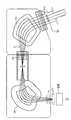
図3を参照し、本開示の1つの具体化によって基材(基板)を加工するために、模範的なシステム300のブロック図が示される。システム300は、ビーム線の粒子システム300であることができる。システム300は、イオン源302、引き出し(抽出)システム304、加速システム306、オプションのビーム操作構成要素308、および中和(無効化)システム310を含むことができる。そのうえ、システム300は、中和システム310と連通する端部ステーション312を含みうる。端部ステーション312は、ウインドウ314および1またはそれよりも多くの負荷ロック(loadlocks)316および318を含むことができる。端部ステーション312内で、基板322を支えるプラテンが置かれうる。そのうえ、1つまたはそれよりも多くの基板移動、冷却および/または加熱サブシステム324が端部ステーション312に配置されうる。
Referring to FIG. 3, a block diagram of an
本開示で、イオン源302はBernas(ベルナス)タイプであることができ、傍熱陰極を有する。この技術の通常の知識を有する者は、イオン源302が他のタイプのイオン源である場合もあると認める。一方、引き出しシステム304は単一のスリット(切れ込み)、またあるいは、多重スリット抽出システム304であることができる。引き出しシステム304は、1つまたはそれよりも多くの直交方向において移すことができる場合がある。そのうえ、引き出しシステム304は、時間的に一定のビーム流を引き出すように設計される場合がある。そのうえ、引き出しシステム304は、連続的に、または断続的に粒子を引き出すことができる。引き出しシステム304はまた、望ましい空間および/または時間的なビームプロファイルを可能にするために、粒子ビームまたはビームレット(beamlets)を集中させることができる。引き出しシステム304によって引き抜かれる粒子ビームは、ほぼ80keVのエネルギーをもつことができる。
In this disclosure, the
より一層高いエネルギーが必要とされる場合、システム300は粒子ビームを速めることができる加速システム306を含みうる。システム300は、ろ過し、スキャンし、および粒子ビームに対し粒子を形作るために、1つまたはそれよりも多くの追加の、オプションのビーム操作構成要素308を含むことができる。図4に図示されるように、システム300の特定の例、オプションのビーム操作構成要素308は、第1の磁石分析機406、第1の減速度(D1)ステージ408、第2の磁石分析機410、および第2の減速度および第2の減速度(D2)ステージ412を含むことができる。本開示では、第1の磁石分析機406、実質的に双極子の磁石は、望ましくない質量および/またはエネルギーの粒子が磁石分析機406を通過しないように、粒子の質量およびエネルギーに基づく粒子をろ過することができる。一方、第2の磁石分析機410、別の実質双極子の磁石は、望ましい形状(例は、リボン)および/または寸法をもつ粒子ビーム中に粒子を平行にするように構成することができる。粒子が望ましいエネルギーで基材に導入されることができるように、D1およびD2の減速度ステージ410および412を浸透する粒子のエネルギーを操作することができる。1種の具体化において、D1および/またはD2は、空間電荷効果を最小にし、そしてビームの空間的完全性を維持することができる分割レンズであることができる。
If even higher energy is required, the
示していないが、ビーム操作構成要素はまた、ビームを焦束するために、1つまたはそれよりも多くの実質四重極の磁石またはアインツェルレンズも含みうる。さらに、ビーム操作構成要素はまた、ビームプロファイルの均一性をコントロールするために米国特許第6,933,507号および第5,350,926号明細書で記述されるような、磁気多重極またはロッドも含みうる。 Although not shown, the beam steering component may also include one or more substantially quadrupole magnets or Einzel lenses to focus the beam. In addition, the beam steering component may also include a magnetic multipole or rod, as described in US Pat. Nos. 6,933,507 and 5,350,926 to control the uniformity of the beam profile.
図3を参照し、電荷中和システム310はまた、本具体化によって、基材322において電荷蓄積を減らすために含まれうる。電荷中和システム310はホットフィラメント、またはマイクロ波、rf(高周波)駆動タイプの1つまたはそれよりも多くのシステムである場合があり、米国特許出願11/376850で記述される。あるいはまた、電荷中和システム310は、電子源である場合がある。
Referring to FIG. 3, a
端部ステーションにおいて、基材周りの環境は、たとえば、基材上で他の材料の堆積を防止するか、または結晶化プロセスを強めるために不動態化を促進するためにコントロールすることができる。環境をコントロールするために、端部ステーション312は、薄いホイルウインドウまたは差動的にポンプで送られる開口314、それを通して粒子は入ることができ、そして1つまたはそれよりも多くの負荷ロック316および318を含み、そしてそれを通して基材が収容されうる。負荷ロック316および318は、1つまたはそれよりも多くの差動的にポンプで送られたステージによって取り替えられることができ、それを通して基材が収容されうる。
At the end station, the environment around the substrate can be controlled, for example, to prevent deposition of other materials on the substrate or to promote passivation to enhance the crystallization process. To control the environment,
端部ステーション312はまた、基材作動機構、冷却、および加熱サブシステム324を含むことができる。サブシステム324の例には、チラー(冷却装置)、熱源、いくつかの軸に沿った基材を移動/回転させることができるロプラト(roplat)を含みうる。チラーの特定の例は、米国特許出願番号第11/504,367号、第11/525,878号および第11/733,445号明細書で見出すことができ、それぞれを参照することによって全体として組み込む。熱源の特定の例は、レーザー、フラッシュランプ(ストロボ)、流体暖房装置を提供するプラテン、抵抗熱源、または米国特許出願第11/770,220号および第11/778,335号明細書に記載のものであることができ、それらの各々を参照することによって全体として組み込む。
The
プロセスおよび基材パラメーター/状態を監視するために1つまたはそれよりも多くのパラメーター/状態を測定する構成要素は、基材322の近くで含まれうる。そのような構成要素は、1つまたはそれよりも多くのコントローラーに連結されるかもしれず、そしてコントローラーは基材のパラメーター/状態および/または測定構成要素からの信号に基づく粒子をコントロールすることができる。
Components that measure one or more parameters / conditions to monitor process and substrate parameters / conditions may be included near the
図5を参照し、本開示の別の具体化によって基材を加工するための別の模範的なシステムが示される。とりわけ、システム500はPLAD、PIIIシステム、または他のプラズマを基にした基材処理システムであることができる。PLADシステム500は、トップセクション(頂部区分)502および下側セクション504を含むチャンバー501を含みうる。トップセクション502は、概して水平方向において延びる第1誘電体セクションおよび概して垂直方向において延びる第2誘電体セクション508を含むことができる。1種の具体化において、各誘電体セクション506および508は、化学的に抵抗性であり、そして良好な熱的特性をもつセラミックであることができる。トップセクション502はまた、少なくとも1つまたはそれよりも多くのアンテナ510および512を含むことができる。1つまたはそれよりも多くのアンテナ510および512は、たとえば、水平アンテナ510および/または垂直アンテナ512であることができる。1種の具体化において、水平アンテナ510は並列巻きをもつ平面コイルであることができ、ところが、垂直アンテナ512は並列巻きの螺旋形コイルであることができる。アンテナ510および512のうちの少なくとも1つは、インピーダンス整合ネットワーク516を介して電源514に電気的につなぐことができる。
Referring to FIG. 5, another exemplary system for processing a substrate according to another embodiment of the present disclosure is shown. In particular, the system 500 can be a PLAD, PIII system, or other plasma-based substrate processing system. The PLAD system 500 can include a chamber 501 that includes a
システム500の下側セクション504上で、プラテン520によって支持されるプラテン520および基板522は、トップセクション502下の予め定められた高さに置くことができる。しかし、またプラテン502および基板522は、トップセクション502に置くことができると考えられる。バイアス電圧電源524はDCへのプラテン520に電気的につなぐことができ、またはRFはプラテン520を偏らせる。
On the
操作において、アンテナ510および512のうちの少なくとも1つは、電源514によって動かされるRFまたはDCであることができる。アンテナ510および512のうちの1種が動かされるRFまたはDCである場合、アンテナ510および512の他の1種は渦流のアンテナであることができる。アンテナ510および512の他の1種は、電源514に電気的につながらないので、渦流のアンテナでありうる。代わりに、アンテナ510および512の他の1つは、電源514で動かされるアンテナに、磁気的につながる。あるいはまた、アンテナ510および512の双方とも、RF流を伴う電源514によって動かされうる。しかる後、アンテナ510および512のうちの少なくとも1つは、第1および第2の誘電体セクション506および508を介してシステム500にRF電流を誘導する。RF電流によって誘導される電磁場は、システム500において含まれるガスがプラズマに変換することができる。一方、バイアス電圧電源524は、基板522にプラズマ中で荷電粒子を引きつけるよう、プラテン520を偏らせるかもしれません。システム500のさらなる詳細は、米特許出願連続番号第11/766984号明細書で見出すことができ、出願公開第2005/0205211号明細書、出願公開第2005/0205212号明細書、および出願公開第2007/0170867号明細書、それらの各々を参照することによって全体として組み込む。
オプションの構成要素
In operation, at least one of
Optional components
上述の構成要素に加えて、模範的なシステム300-500は、粒子供給源(例は、イオン源またはプラズマ)および基材の間で1つまたはそれよりも多くのマスクを随意に含むことができる。含まれる場合、マスクは選択的にカーボン(C)を基にした物質、Siを基にした物質(例は、SiC)、または耐火性金属、例は、WまたはTaのようなもの、含有する材料である場合がある。しかし、他の材料もまた用いることができる。そのようなマスクは、基材上でビーム入射の形状をコントロールするために、山形形状を含む種々の形状をもつ1つまたはそれよりも多くの開口をもちうる。
FPD
In addition to the components described above, the exemplary systems 300-500 optionally include one or more masks between the particle source (eg, ion source or plasma) and the substrate. it can. When included, the mask optionally contains carbon (C) based material, Si based material (eg SiC), or refractory metal, eg something like W or Ta It may be a material. However, other materials can also be used. Such a mask may have one or more apertures with various shapes, including chevron shapes, to control the shape of the beam incidence on the substrate.
FPD
下に、粒子によって誘導された相転換のいくつかの応用適用の説明を提供する。上記したように、粒子はアモルファスのものから結晶相まで相転換を誘導するために、薄膜基材のSi層中に導入することができる。明快さの目的のために、粒子によって誘発された相転換の比較を、ELAプロセスで行う。 Below, a description of some application applications of particle-induced phase transformation is provided. As described above, the particles can be introduced into the Si layer of the thin film substrate in order to induce phase transition from amorphous to crystalline phase. For the purpose of clarity, a comparison of the particle-induced phase change is made in the ELA process.
本具体化において、粒子は、絶縁性フィルム上に配置されたおよそ500Åの厚さアモルファスのSiフィルムをもつFPDに向けられうる。絶縁性フィルムは、たとえば、およそ0.7mmの、石英、プラスチック、またはサファイヤの厚さをもつアモルファスガラスまたはCorning(コーニング)1737ガラスでありうる。しかし、この技術の通常の知識を有する者は、他のタイプの絶縁膜も使われるかもしれないと認めます。 In this embodiment, the particles can be directed to an FPD having an amorphous Si film of approximately 500 mm thickness disposed on an insulating film. The insulating film can be, for example, amorphous glass with a thickness of quartz, plastic or sapphire of approximately 0.7 mm or Corning 1737 glass. However, those with ordinary knowledge of this technology admit that other types of insulation may also be used.
ELAプロセスにおいて、単一のレーザーパルスは、長さ12ナノ秒のパルスで、360mJ/cm2のエネルギーパルスを送ることができる。これは、3×1010W/m2を出力密度と同等に考えられる。ArイオンビームがSiフィルムに向けられる場合、ビームは20keVのエネルギーをもちうる。そのようなエネルギーを伴い、指向されたArイオンのすべてが、Si層(図2参照)を超えて、基材を透過するというわけではないかもしれない。リボン形状のAr粒子ビームが使われる場合、ビームは高さ0.1mmによる幅300mmの寸法をもつとされるかもしれない。25mAのビーム電流を伴って、これは1.7×107W/m2の出力密度を意味する。 In ELA process, a single laser pulse with a pulse length 12 ns, it is possible to send a pulse of energy 360 mJ / cm 2. This is considered to be 3 × 10 10 W / m 2 equivalent to the power density. When an Ar ion beam is directed at a Si film, the beam can have an energy of 20 keV. With such energy, not all directed Ar ions may penetrate the substrate beyond the Si layer (see Figure 2). If a ribbon-shaped Ar particle beam is used, the beam may be assumed to have a width of 300 mm with a height of 0.1 mm. With a beam current of 25 mA, this means a power density of 1.7 × 10 7 W / m 2 .
ELAプロセスにおいて、基材上でのレーザービーム入射は、Si層を1000℃に、アモルファスSiの融解温度の近くで加熱するかもしれない。入射により、レーザービームはSi層の少なくとも部分的な溶解を始めうる。Siのための熱の拡散係数は比較的高く、そして、室温で〜1cm2/秒および1400Kでの0.1cm2/秒の間で変動する。それゆえに、たとえレーザーエネルギーがSi表面の頂部の数nm(2、3nm)において吸収されるとしても、何らかの潜熱効果なしででも、非常に小さな温度勾配がSi層内にあるかもしれない。熱は、ガラスにSiから拡散することができる。ガラスのための拡散率は小さく(多数の(a large)温度範囲にわたり〜0.005cm2/s)、そしてそれで、多数の熱勾配が厚いガラス層を横切って存在しうる。図6において示されるモデルの結果は、ガラスがSiの0.1μm内でさえ、500℃より高くに達しないことを計算出する。 In the ELA process, laser beam incidence on the substrate may heat the Si layer to 1000 ° C. near the melting temperature of amorphous Si. Upon incidence, the laser beam can begin to at least partially dissolve the Si layer. The diffusion coefficient of heat for Si is relatively high, and varies between 0.1 cm 2 / sec at 1 cm 2 / sec and 1400K at room temperature. Therefore, even if the laser energy is absorbed at the top few nm (2, 3 nm) of the Si surface, there may be a very small temperature gradient in the Si layer without any latent heat effect. Heat can diffuse from the Si into the glass. The diffusivity for the glass is small (˜0.005 cm 2 / s over a large temperature range), so multiple thermal gradients can exist across the thick glass layer. The model results shown in FIG. 6 calculate that the glass does not reach above 500 ° C. even within 0.1 μm of Si.
粒子ビームがより一層低い出力密度をもつもつので、Siフィルムを加熱するのに十分なエネルギーをデポするために必要な露出時間はレーザー(12ns)と比較して高いことがある(80ms)。そのうえ、粒子を介して基材にデポされる熱は熱伝導を介する絶縁(処理)に欠失されているかもしれず、より一層多くのエネルギーは十分にSiフィルムを加熱するために必要であるかもしれない。これらの仮定の下で、Siの50μm内の絶縁性フィルムは、600℃を超えて加熱することができる。それでも、これらの状態が許容されうるように、絶縁の十分な量はそのガラス転移(または融解)温度より上に加熱されないことがある。 Because the particle beam has a much lower power density, the exposure time required to deposit enough energy to heat the Si film can be higher (80 ms) compared to the laser (12 ns). Moreover, the heat deposited on the substrate via the particles may be lost to insulation (treatment) via heat conduction, and more energy may be needed to sufficiently heat the Si film. unknown. Under these assumptions, insulating films within 50 μm of Si can be heated above 600 ° C. Nevertheless, a sufficient amount of insulation may not be heated above its glass transition (or melting) temperature so that these conditions can be tolerated.
リボンビームの高さが1mmまで増加された場合、Siフィルムを十分に加熱するためにおよそ2.4秒がかかるかもしれず、その時間で、ガラスの底のピーク温度が600℃に達することがある。この例は、図7における0.1mmのケースと比較して、ビームの出力密度をできるだけ高く保つ必要性を例示する。これは、ビームエリアをできるだけ小さく保つこと、ビーム流を増やすこと、および/またはビームエネルギーを増やすことによって達成されうる。イオン種の量もまた、増加させることができる。分子粒子ビームの使用は、それがより一層高いビームエネルギーの使用を許すので望ましい場合がある。同時に、より一層高いビームエネルギーは、追加の有害な結果で、たとえば、さもなければビーム電流を制限するかもしれない空間電荷破裂(blow-up)およびおよびビーム集束のようなものを減らすことができる。 If the ribbon beam height is increased to 1 mm, it may take approximately 2.4 seconds to fully heat the Si film, during which time the peak temperature at the bottom of the glass may reach 600 ° C. This example illustrates the need to keep the beam power density as high as possible compared to the 0.1 mm case in FIG. This can be achieved by keeping the beam area as small as possible, increasing the beam flow, and / or increasing the beam energy. The amount of ionic species can also be increased. The use of a molecular particle beam may be desirable because it allows the use of a higher beam energy. At the same time, higher beam energy can reduce additional detrimental consequences such as space charge burst-up and beam focusing that might otherwise limit the beam current. .
粒子ビーム照射はアモルファス相において固体Siを保持することができ、溶解を1300Kで起きるのを可能にする。結晶質のSiは、1683Kまで溶けない。したがって、溶解が始まる前にアモルファスSiが結晶化を経るならば、より一層多くの出力は完全に材料を溶かすことを要求されうる。また、液体Siはレーザー放射の一部分を反映するかもしれず、そしてそれで、一旦Si表面が溶ける場合、Siのバルク中へのカップリングパワー(結合力)は困難なことがある。冷却および結晶化相中の粒子ビームの存在は、高品質物質の生産に影響を及ぼすことがある。
薄膜太陽電池
Particle beam irradiation can retain solid Si in the amorphous phase and allows dissolution to occur at 1300K. Crystalline Si does not melt up to 1683K. Thus, if amorphous Si undergoes crystallization before dissolution begins, more power can be required to completely dissolve the material. Also, liquid Si may reflect a portion of the laser radiation, and so once the Si surface melts, the coupling power into the bulk of Si may be difficult. The presence of a particle beam in the cooling and crystallization phase can affect the production of high quality material.
Thin film solar cell
本開示において記載する粒子誘導された相転換はまた、薄膜太陽電池の製造にも適用されうる。この技術で知られるように、アモルファスSiは直接的なバンドギャップ物質であり、そして結晶質のSi、間接的バンドギャップ物質よりも効率的に光を吸収することができる。そのうえ、アモルファスSiは、結晶質のSiよりも多くの光を可視スペクトルにおいて吸収する。しかし、アモルファスSiは、より一層低い電気伝導度をもつ。そのように、アモルファスSiは、入射光を電流に転換するのが好ましいかもしれず、一方で、結晶質のSiは、発生する電流を移すのが好ましいかもしれない。したがって、太陽電池は、本具体化によって、結晶質のSiの別の層より上に、アモルファスSiの層をもつのが好ましい場合がある。可視光線での入射光は、アモルファスSiで光電流に効率的に変換されうる。アモルファス層(赤外線を含む)において変換されない光は、結晶質のSiにおいて光電流に変換されうる。 The particle-induced phase change described in this disclosure can also be applied to the manufacture of thin film solar cells. As is known in the art, amorphous Si is a direct bandgap material and can absorb light more efficiently than crystalline Si, an indirect bandgap material. In addition, amorphous Si absorbs more light in the visible spectrum than crystalline Si. However, amorphous Si has a much lower electrical conductivity. As such, amorphous Si may preferably convert incident light into current, while crystalline Si may preferably transfer the generated current. Accordingly, the solar cell may preferably have an amorphous Si layer above another crystalline Si layer according to this embodiment. Incident light in visible light can be efficiently converted into photocurrent by amorphous Si. Light that is not converted in the amorphous layer (including infrared) can be converted into photocurrent in crystalline Si.
図8を参照し、本開示の別の具体化によって、基材を調製するのに組み込むことができるプロセスが示される。本具体化において、基材は結晶およびアモルファスの層を有する薄膜太陽電池であることができる。別の具体化において、基材は絶縁層(示さず)に配置されるFPDの半導電性層であることができる。図8Aに例示するように、アモルファスSi層802はガラス層(示さず)上に堆積することができる。Si層802は1.5μmの厚さをもつことができ、一方、ガラス層は3mmの厚さをもつことができる。予め定められた用量およびエネルギーをもつ粒子804は、次いでアモルファスSi層802に導入されうる。図8Bに例示するように、粒子804はSi層802の下側部分を結晶化させるために、アモルファスSi層802の上側部分の具体化を誘導することなく、Si層の表面の下に導入することができる。結果として生じる基材は、結晶Si層806上に堆積されたアモルファスSi層802をもつ太陽電池において用いることができる。
Referring to FIG. 8, another embodiment of the present disclosure shows a process that can be incorporated to prepare a substrate. In this embodiment, the substrate can be a thin film solar cell having crystalline and amorphous layers. In another embodiment, the substrate can be a FPD semiconductive layer disposed on an insulating layer (not shown). As illustrated in FIG. 8A, an
図9を参照し、本開示の別の具体化によって基材を調製することで組み込むことができるプロセスが示される。本具体化において、基材は結晶質の、およびアモルファスの層を有する薄膜太陽電池であることができる。別の具体化において、基材は絶縁層(示さず)上に配置されるFPDの半導電性層でありうる。図9Aに例示するように、アモルファスSi層902はガラス層(示さず)上に堆積することができる。しかる後、予め定められた用量およびエネルギーをもつ粒子904は、全体のSi層906(図9B)を結晶化するために、アモルファスSi層902に導入することができる。図9Cに例示するように、複数の粒子の第2の種908、エネルギー、および用量は、結晶質のSi層の表面の近くの層をアモルファス化するために、基材に導入することができる。結果として生じる太陽電池は、アモルファスの頂部のSi層904および結晶質の下側のSi層902をもつことができる。
Referring to FIG. 9, a process that can be incorporated by preparing a substrate according to another embodiment of the present disclosure is shown. In this embodiment, the substrate can be a thin film solar cell having crystalline and amorphous layers. In another embodiment, the substrate can be a semiconductive layer of FPD disposed on an insulating layer (not shown). As illustrated in FIG. 9A, an
図10を参照し、本開示の別の具体化によって基材を調製することにおいて組み込むことができるプロセスが示される。本具体化において、基材は結晶質の、およびアモルファスの層を有する薄膜太陽電池であることができる。別の具体化において、基材は絶縁層(示さず)上に配置されるFPDの半導電性層でありうる。図10Aに例示するように、アモルファスSi層1002はガラス層(示さず)上に堆積されるかもしれない。しかる後、予め定められた用量およびエネルギーをもつ粒子1004は、Si層1002(図10B)内でサブレイヤー(副層)1006を結晶化させるために、アモルファスSi層1002に導入することができる。図10BはサブレイヤーがSi層1002の上側表面の近くで配置されたことを例示するが、この技術の通常の知識を有する者は、サブレイヤー1006が、上側表面の近くで、下側表面の近くで、またはSi層1002の上側表面および下側表面の間でどこかに置くことができるのを認識するべきである。
Referring to FIG. 10, a process that can be incorporated in preparing a substrate according to another embodiment of the present disclosure is shown. In this embodiment, the substrate can be a thin film solar cell having crystalline and amorphous layers. In another embodiment, the substrate can be a semiconductive layer of FPD disposed on an insulating layer (not shown). As illustrated in FIG. 10A, an
結晶質のサブレイヤー1006を形成した後、サブレイヤー1006での結晶の1つまたはそれよりも多くのものは、全体のSi層1002を結晶化することができるまで、サブレイヤー1006から離れて成長させることができる。結晶は、炉アニーリング、迅速な熱的アニーリング(RTA)、フラッシュランプアニーリング、およびレーザーアニーリングのうちの1つを介して成長することができる。あるいはまた、結晶は粒子アシストアニーリングによって成長させることができる。たとえば、同じ、または別のタイプの粒子(示さず)は、予め定めた用量および/または別の予め定めたエネルギーを、基材の下側表面の方へ1またはそれよりも多くの結晶の粒界を延ばすために、結晶化されたサブレイヤーの下の領域に対してもつ。このプロセスでは、全体のSi層1002は、垂直方向において延びる粒界をもつ1またはそれよりも多くの結晶を含むことができる。本具体化ではまた、新しく結晶化されたSi層1006の1部分をアモルファス化するために、随意のアモルファス化ステップを含むことができる。たとえば、粒子1010は次いで、新しく結晶化されたSi層1002の少なくとも1部分(図10D)をアモルファス化し、アモルファスのサブレイヤー1012を形成するために、新しく結晶化されたSi層1002に導入することができる。本開示で、粒子を、新しい結晶質のSi層1002の粒子で、前のアモルファスSi層1002を結晶化させるために用いたものと同じ粒子に導入した。代わりに、新しい結晶質のSi層1002に導入された粒子は、前のアモルファスSi層1002を結晶化させるのに用いられたそれらのものとは異なることがある。上記のプロセスは、厚いアモルファスSi層を結晶化させるのに用いることができる。
After forming the
粒子で誘導された相転換はまた、効率的な多結晶Si太陽電池を製造するのにも用いることができる。結晶の粒界は、ゲッタリング(残留ガス除去)不純物で、たとえば金属汚染物質のようなもののための効果的な部位でありうる。そのうえ、粒界は電荷担体の移動性のためのバリア(障壁)として働くことができ、キャリヤーが境界を通してトラベルするのが妨げられる。したがって、多重の結晶をもつ多結晶太陽電池は、このように、多重の粒界は、粒界が電荷担体の通路を横切って位置付けられる場合、比較的低い電気伝導度をもつことができる。多結晶太陽電池において、上側表面で生じる電流は接触エリアへ運搬されなければならず、それは概して、太陽電池の下側表面に位置付けられる。多結晶太陽電池での粒界が電荷担体の通路を横切って置かれる場合、太陽電池の効率は下げられるかもしれない。そのように、粒界を電荷担体の通路と比較して平行な仕方において配向された粒界をもつ多結晶太陽電池を製造することは、望ましい場合がある。 Particle-induced phase transformation can also be used to produce efficient polycrystalline Si solar cells. Crystal grain boundaries can be effective sites for gettering (residual gas removal) impurities, such as metal contaminants. In addition, the grain boundaries can act as a barrier for charge carrier mobility, preventing the carriers from traveling through the boundary. Thus, a polycrystalline solar cell with multiple crystals can thus have a relatively low electrical conductivity when multiple grain boundaries are positioned across the charge carrier path. In polycrystalline solar cells, the current generated at the upper surface must be carried to the contact area, which is generally located on the lower surface of the solar cell. If the grain boundaries in a polycrystalline solar cell are placed across the charge carrier path, the efficiency of the solar cell may be reduced. As such, it may be desirable to produce a polycrystalline solar cell with grain boundaries oriented in a parallel manner comparing the grain boundaries to the charge carrier paths.
効率的な多結晶太陽電池を製造するために、アモルファスSi基材を調製がすることができる。しかる後、Si層の上側表面は結晶化されることができ、そして結晶は固相エピタキシャル再成長(SPER)につき下方に成長することができる。基材に送られる出力密度が最大にされることがないように、イオンエネルギーを選ぶことができる。これは、40から100kevまでの間でのエネルギーと対応するかもしれず、そこでは典型的なイオンビームシステムが最大のビーム電流をイオン源から引き出すことができ、そして空間電荷効果がビーム輸送および集束のために減らされる。そのようなイオンビームは、全部の層が結晶化されるまで、下方に順にSPERをシードすることができるシリコンの表面の近くで、結晶化を引き起こしうる。SPERが、ビームで誘導された結晶化ステップの一部として、または1つまたはそれよりも多くの炉、RTA、フラッシュランプ、レーザーまたは他のアニーリング方法を用いることができる更なるアニーリングステップにおいて起こりうる。結果として生じる基材は、垂直に延びる粒界をを有する結晶をもつと思われる。しかる後、第2の種の粒子、エネルギーおよび用量は、多結晶基材の表面の近くで層をアモルファス化するために基材に導入されうる。太陽電池は次いで、垂直に延びる多結晶Si層上のアモルファスSi層の構造をもつことができる。上記したように、そのような太陽電池は、より一層効率的に、放射エネルギーを電気エネルギーに変換し、および同時に、より一層効率的に変換される電気エネルギーを運搬すると思われる。 In order to produce an efficient polycrystalline solar cell, an amorphous Si substrate can be prepared. Thereafter, the upper surface of the Si layer can be crystallized and the crystal can grow down for solid phase epitaxial regrowth (SPER). The ion energy can be chosen so that the power density delivered to the substrate is not maximized. This may correspond to energies between 40 and 100 kev, where a typical ion beam system can extract the maximum beam current from the ion source, and space charge effects can be used for beam transport and focusing. To be reduced. Such an ion beam can cause crystallization near the surface of the silicon that can be seeded sequentially with SPER down until all layers are crystallized. SPER can occur as part of a beam-induced crystallization step or in further annealing steps where one or more furnaces, RTA, flash lamps, lasers or other annealing methods can be used . The resulting substrate appears to have crystals with vertically extending grain boundaries. Thereafter, the second species of particles, energy and dose can be introduced into the substrate to amorphize the layer near the surface of the polycrystalline substrate. The solar cell can then have the structure of an amorphous Si layer on a vertically extending polycrystalline Si layer. As noted above, such solar cells are believed to more efficiently convert radiant energy to electrical energy and at the same time carry electrical energy that is more efficiently converted.
本開示において、境界のサイズおよび方向付けは、頂部層の結晶化をアシスト(援助)するのに用いられる粒子ビーム状態の選定によって影響されうる。リンは好ましい種であるかもしれないが、実際には良好なゲッター種であり、そして太陽電池のための一般に好まれるドーパントでありうる。注入の方向は、粒子配向に影響するように選ぶことができる。全部の活動層を埋め込むことができ、または表面層は、少ない空隙率しか有さない頂部結晶質表面をつくらないように埋め込むことができ、そして残りの基材はSPERによって再成長されうる。 In the present disclosure, the size and orientation of the boundary can be influenced by the choice of particle beam conditions used to assist crystallization of the top layer. Phosphorus may be a preferred species, but in fact it is a good getter species and may be a generally preferred dopant for solar cells. The direction of implantation can be chosen to affect the particle orientation. The entire active layer can be embedded, or the surface layer can be embedded so as not to create a top crystalline surface with low porosity, and the remaining substrate can be regrown by SPER.
ここで採用された用語および表現は、説明の条件として用いてあり、そして制限するものでなく、およびそのような用語および表現の使用において、示されて、また説明されたた特長の何らかの等価物(またはその部分)も除外する意図はなく、および種々の修飾が請求の範囲内で可能であることが認識される。他の修飾、変形、および代替物もまた可能である。したがって、前述の説明は例証としてだけのものであり、そして制限するように意味されない。請求されるものは、ここに詳述された何らかの特長である。
The terms and expressions employed herein are used as conditions for explanation and are not limiting, and any equivalent of the features shown and described in the use of such terms and expressions (Or portions thereof) are not intended to be excluded, and it will be appreciated that various modifications are possible within the scope of the claims. Other modifications, variations, and alternatives are also possible. Accordingly, the foregoing description is by way of example only and is not meant as limiting. What is claimed is any feature detailed herein.
Claims (34)
基材の第1の領域に対して、第1の領域において粒界をもつ少なくとも1種の結晶が第2の領域で別の結晶を形成することなく形成されるように、複数の第1の粒子を導入することであり、第2の領域は第1の領域に隣接するもの、および
第1の領域において形成された少なくとも1種の結晶の粒界を、複数の第1の粒子の導入の停止後に、第2の領域に延ばすこと
を含む方法。 A method for preparing a substrate in an amorphous phase, wherein at least one crystal having a grain boundary in the first region is different in the second region relative to a first region of the substrate: Introducing a plurality of first particles so that they are formed without forming crystals, wherein the second region is adjacent to the first region and at least one formed in the first region; Extending the seed crystal grain boundary to the second region after stopping the introduction of the plurality of first particles.
第1の領域の少なくとも1部分をアモルファスにするために、複数の第2の粒子を第1の領域の少なくとも1部分に導入すること
を含む、請求項1の方法。 The method of claim 1, further comprising introducing a plurality of second particles into at least a portion of the first region to render at least a portion of the first region below amorphous.
第1の粒子を第1の領域に導入するのに先立ち、基材の温度を変化させること
を含む、請求項1の方法。 The method of claim 1, further comprising changing the temperature of the substrate prior to introducing the following first particles into the first region.
The method of claim 1, wherein the first particles are introduced into the first region at an angle other than an angle perpendicular to the upper surface of the substrate.
Applications Claiming Priority (5)
| Application Number | Priority Date | Filing Date | Title |
|---|---|---|---|
| US98765007P | 2007-11-13 | 2007-11-13 | |
| US98766707P | 2007-11-13 | 2007-11-13 | |
| US98762907P | 2007-11-13 | 2007-11-13 | |
| US12/269,344 US8003498B2 (en) | 2007-11-13 | 2008-11-12 | Particle beam assisted modification of thin film materials |
| PCT/US2008/083388 WO2009064872A2 (en) | 2007-11-13 | 2008-11-13 | Particle beam assisted modifcation of thin film materials |
Publications (2)
| Publication Number | Publication Date |
|---|---|
| JP2011503882A true JP2011503882A (en) | 2011-01-27 |
| JP2011503882A5 JP2011503882A5 (en) | 2012-01-05 |
Family
ID=40624096
Family Applications (3)
| Application Number | Title | Priority Date | Filing Date |
|---|---|---|---|
| JP2010533345A Withdrawn JP2011503882A (en) | 2007-11-13 | 2008-11-13 | Particle beam assisted modification of thin film materials |
| JP2010533346A Withdrawn JP2011503883A (en) | 2007-11-13 | 2008-11-13 | Improvement of thin film materials with particle beam assistance |
| JP2010533344A Pending JP2011505685A (en) | 2007-11-13 | 2008-11-13 | Improvement of thin film materials with particle beam assistance |
Family Applications After (2)
| Application Number | Title | Priority Date | Filing Date |
|---|---|---|---|
| JP2010533346A Withdrawn JP2011503883A (en) | 2007-11-13 | 2008-11-13 | Improvement of thin film materials with particle beam assistance |
| JP2010533344A Pending JP2011505685A (en) | 2007-11-13 | 2008-11-13 | Improvement of thin film materials with particle beam assistance |
Country Status (6)
| Country | Link |
|---|---|
| US (3) | US20090124065A1 (en) |
| JP (3) | JP2011503882A (en) |
| KR (3) | KR20100105595A (en) |
| CN (3) | CN101897006A (en) |
| TW (3) | TW200943432A (en) |
| WO (3) | WO2009064867A2 (en) |
Families Citing this family (19)
| Publication number | Priority date | Publication date | Assignee | Title |
|---|---|---|---|---|
| EP2308060A4 (en) * | 2008-06-11 | 2013-10-16 | Intevac Inc | Application specific implant system and method for use in solar cell fabrications |
| US20100053817A1 (en) * | 2008-09-04 | 2010-03-04 | Robert Glenn Biskeborn | Coated magnetic head and methods for fabrication thereof |
| WO2010121309A1 (en) * | 2009-04-21 | 2010-10-28 | Petar Branko Atanackovic | Optoelectronic device with lateral pin or pin junction |
| FR2946335B1 (en) * | 2009-06-05 | 2011-09-02 | Saint Gobain | THIN LAYER DEPOSITION METHOD AND PRODUCT OBTAINED |
| US8749053B2 (en) | 2009-06-23 | 2014-06-10 | Intevac, Inc. | Plasma grid implant system for use in solar cell fabrications |
| US20110039034A1 (en) * | 2009-08-11 | 2011-02-17 | Helen Maynard | Pulsed deposition and recrystallization and tandem solar cell design utilizing crystallized/amorphous material |
| TWI459444B (en) * | 2009-11-30 | 2014-11-01 | Applied Materials Inc | Crystallization processing for semiconductor applications |
| KR101991882B1 (en) * | 2011-05-13 | 2019-06-21 | 가부시키가이샤 사무코 | Method for manufacturing semiconductor epitaxial wafer, semiconductor epitaxial wafer, and method for manufacturing solid-state image pickup element |
| KR20120131753A (en) * | 2011-05-26 | 2012-12-05 | 삼성디스플레이 주식회사 | Thin film transistor, method of manufacturing thin film transistor, and organic light emitting diode display |
| US8652974B2 (en) * | 2011-06-22 | 2014-02-18 | Ipg Photonics Corporation | Method and system for pre-heating of semiconductor material for laser annealing and gas immersion laser doping |
| US9324598B2 (en) | 2011-11-08 | 2016-04-26 | Intevac, Inc. | Substrate processing system and method |
| MY178951A (en) | 2012-12-19 | 2020-10-23 | Intevac Inc | Grid for plasma ion implant |
| CN106898540B (en) * | 2015-12-17 | 2020-01-31 | 宸鸿光电科技股份有限公司 | Semiconductor manufacturing method |
| DE102017119571B4 (en) | 2017-08-25 | 2024-03-14 | Infineon Technologies Ag | ION IMPLANTATION METHOD AND ION IMPLANTATION DEVICE |
| JP6812962B2 (en) * | 2017-12-26 | 2021-01-13 | 株式会社Sumco | Manufacturing method of epitaxial silicon wafer |
| CN111668353B (en) * | 2020-06-19 | 2021-12-17 | 錼创显示科技股份有限公司 | Light emitting semiconductor structure and semiconductor substrate |
| TWI728846B (en) | 2020-06-19 | 2021-05-21 | 錼創顯示科技股份有限公司 | Light-emitting semiconductor structure and light-emitting semiconductor substrate |
| KR20230065341A (en) * | 2020-10-30 | 2023-05-11 | 사이머 엘엘씨 | Optical Components for Deep Ultraviolet Light Sources |
| CN117374146A (en) * | 2023-12-06 | 2024-01-09 | 山东大学 | Semiconductor detector and energy self-calibration and state monitoring method thereof |
Family Cites Families (31)
| Publication number | Priority date | Publication date | Assignee | Title |
|---|---|---|---|---|
| JPS5758315A (en) | 1980-09-25 | 1982-04-08 | Toshiba Corp | Manufacture of semiconductor single crystal film |
| JPS57148341A (en) * | 1981-03-09 | 1982-09-13 | Nippon Telegr & Teleph Corp <Ntt> | Crystal growth of amorphous layer or polycrystalline layer on single crystal layer |
| US4622093A (en) * | 1983-07-27 | 1986-11-11 | At&T Bell Laboratories | Method of selective area epitaxial growth using ion beams |
| JPS6037719A (en) * | 1983-08-10 | 1985-02-27 | Seiko Epson Corp | Manufacture of semiconductor device |
| JP2595525B2 (en) * | 1987-04-10 | 1997-04-02 | ソニー株式会社 | Method of forming semiconductor thin film |
| JPH0319321A (en) * | 1989-06-16 | 1991-01-28 | Fujitsu Ltd | Formation of semiconductor crystal |
| JP2726118B2 (en) * | 1989-09-26 | 1998-03-11 | キヤノン株式会社 | Deposition film formation method |
| JP2662058B2 (en) * | 1989-11-14 | 1997-10-08 | 日本板硝子株式会社 | Method for manufacturing semiconductor film |
| JPH04294523A (en) * | 1991-03-22 | 1992-10-19 | Toshiba Corp | Manufacture of semiconductor device |
| JP2662321B2 (en) * | 1991-05-31 | 1997-10-08 | 科学技術振興事業団 | Surface treatment method using ultra-slow cluster ion beam |
| JPH0529215A (en) * | 1991-07-22 | 1993-02-05 | Nippon Telegr & Teleph Corp <Ntt> | Beam annealing method |
| JP3194608B2 (en) * | 1991-11-15 | 2001-07-30 | 株式会社ニューラルシステムズ | Recrystallization method by beam irradiation of neutral particles |
| US5350926A (en) * | 1993-03-11 | 1994-09-27 | Diamond Semiconductor Group, Inc. | Compact high current broad beam ion implanter |
| JP3450376B2 (en) | 1993-06-12 | 2003-09-22 | 株式会社半導体エネルギー研究所 | Method for manufacturing semiconductor device |
| EP0652308B1 (en) * | 1993-10-14 | 2002-03-27 | Neuralsystems Corporation | Method of and apparatus for forming single-crystalline thin film |
| US6884698B1 (en) * | 1994-02-23 | 2005-04-26 | Semiconductor Energy Laboratory Co., Ltd. | Method for manufacturing semiconductor device with crystallization of amorphous silicon |
| JPH09153458A (en) * | 1995-09-26 | 1997-06-10 | Fujitsu Ltd | Thin-film semiconductor device and manufacture thereof |
| JP3841910B2 (en) | 1996-02-15 | 2006-11-08 | 株式会社半導体エネルギー研究所 | Method for manufacturing semiconductor device |
| JPH10256153A (en) | 1997-03-17 | 1998-09-25 | Nippon Telegr & Teleph Corp <Ntt> | Method for converting amorphous si layer to single crystal at low temperature |
| US6200631B1 (en) * | 1997-10-27 | 2001-03-13 | Praxair Technology, Inc. | Method for producing corrosion resistant refractories |
| KR19990050318A (en) | 1997-12-17 | 1999-07-05 | 윤덕용 | Crystallization Method of Amorphous Silicon Thin Film by Low Temperature Process |
| US6130436A (en) * | 1998-06-02 | 2000-10-10 | Varian Semiconductor Equipment Associates, Inc. | Acceleration and analysis architecture for ion implanter |
| US6635880B1 (en) * | 1999-10-05 | 2003-10-21 | Varian Semiconductor Equipment Associates, Inc. | High transmission, low energy beamline architecture for ion implanter |
| JP4869504B2 (en) * | 2000-06-27 | 2012-02-08 | 株式会社半導体エネルギー研究所 | Method for manufacturing semiconductor device |
| DE60118070T2 (en) * | 2001-09-04 | 2006-08-17 | Advantest Corp. | Particle beam apparatus |
| US6933507B2 (en) * | 2002-07-17 | 2005-08-23 | Kenneth H. Purser | Controlling the characteristics of implanter ion-beams |
| TW569350B (en) * | 2002-10-31 | 2004-01-01 | Au Optronics Corp | Method for fabricating a polysilicon layer |
| US20070184190A1 (en) * | 2003-08-27 | 2007-08-09 | Mineo Hiramatsu | Method for producing carbon nanowalls, carbon nanowall, and apparatus for producing carbon nanowalls |
| US20060113489A1 (en) * | 2004-11-30 | 2006-06-01 | Axcelis Technologies, Inc. | Optimization of beam utilization |
| JP2006245326A (en) | 2005-03-03 | 2006-09-14 | A.S.K.株式会社 | Single crystal silicon thin-film transistor |
| KR101390442B1 (en) * | 2005-12-07 | 2014-04-30 | 베리안 세미콘덕터 이큅먼트 어소시에이츠, 인크. | Techniques for preventing parasitic beamlets from affecting ion implantation |
-
2008
- 2008-11-12 US US12/269,327 patent/US20090124065A1/en not_active Abandoned
- 2008-11-12 US US12/269,276 patent/US20090124064A1/en not_active Abandoned
- 2008-11-12 US US12/269,344 patent/US8003498B2/en not_active Expired - Fee Related
- 2008-11-13 JP JP2010533345A patent/JP2011503882A/en not_active Withdrawn
- 2008-11-13 CN CN2008801202022A patent/CN101897006A/en active Pending
- 2008-11-13 CN CN2008801245314A patent/CN101911255A/en active Pending
- 2008-11-13 JP JP2010533346A patent/JP2011503883A/en not_active Withdrawn
- 2008-11-13 JP JP2010533344A patent/JP2011505685A/en active Pending
- 2008-11-13 TW TW097143914A patent/TW200943432A/en unknown
- 2008-11-13 KR KR1020107012810A patent/KR20100105595A/en not_active Application Discontinuation
- 2008-11-13 WO PCT/US2008/083382 patent/WO2009064867A2/en active Application Filing
- 2008-11-13 WO PCT/US2008/083391 patent/WO2009064875A1/en active Application Filing
- 2008-11-13 KR KR1020107012811A patent/KR20100106374A/en not_active Application Discontinuation
- 2008-11-13 TW TW097143919A patent/TW200941550A/en unknown
- 2008-11-13 WO PCT/US2008/083388 patent/WO2009064872A2/en active Application Filing
- 2008-11-13 CN CN2008801244595A patent/CN101911250A/en active Pending
- 2008-11-13 KR KR1020107012827A patent/KR20100086042A/en not_active Application Discontinuation
- 2008-11-13 TW TW097143912A patent/TW200941549A/en unknown
Also Published As
| Publication number | Publication date |
|---|---|
| WO2009064875A1 (en) | 2009-05-22 |
| CN101911250A (en) | 2010-12-08 |
| TW200943432A (en) | 2009-10-16 |
| TW200941550A (en) | 2009-10-01 |
| TW200941549A (en) | 2009-10-01 |
| CN101897006A (en) | 2010-11-24 |
| KR20100105595A (en) | 2010-09-29 |
| WO2009064867A2 (en) | 2009-05-22 |
| US8003498B2 (en) | 2011-08-23 |
| KR20100086042A (en) | 2010-07-29 |
| US20090124065A1 (en) | 2009-05-14 |
| WO2009064872A3 (en) | 2009-07-02 |
| WO2009064867A3 (en) | 2009-07-02 |
| KR20100106374A (en) | 2010-10-01 |
| US20090124066A1 (en) | 2009-05-14 |
| US20090124064A1 (en) | 2009-05-14 |
| CN101911255A (en) | 2010-12-08 |
| JP2011505685A (en) | 2011-02-24 |
| WO2009064872A2 (en) | 2009-05-22 |
| JP2011503883A (en) | 2011-01-27 |
Similar Documents
| Publication | Publication Date | Title |
|---|---|---|
| JP2011503882A (en) | Particle beam assisted modification of thin film materials | |
| Rebohle et al. | A review of thermal processing in the subsecond range: semiconductors and beyond | |
| US8067302B2 (en) | Defect-free junction formation using laser melt annealing of octadecaborane self-amorphizing implants | |
| AU2021236824B2 (en) | All-semiconductor Josephson junction device for qubit applications | |
| JP2013502076A (en) | Tandem solar cell structure utilizing pulse deposition and recrystallization and crystallization / amorphous materials | |
| Batalov et al. | Pulsed laser annealing of highly doped Ge: Sb layers deposited on different substrates | |
| US8815719B2 (en) | Defect-free junction formation using octadecaborane self-amorphizing implants | |
| Robinson | Laser Annealing: Processing Semiconductors Without a Furnace | |
| US11195732B2 (en) | Low thermal budget annealing | |
| JP3539738B2 (en) | Impurity addition method | |
| Rebohle et al. | Semiconductor Applications | |
| Skorupa et al. | Advanced thermal processing of semiconductor materials in the msec-range | |
| US20130045557A1 (en) | Deposition of porous films for thermoelectric applications | |
| Zhou et al. | Application of Sub-second Annealing for Diluted Ferromagnetic Semiconductors | |
| JP2004303920A (en) | Semiconductor thin film manufacturing apparatus |
Legal Events
| Date | Code | Title | Description |
|---|---|---|---|
| A521 | Request for written amendment filed |
Free format text: JAPANESE INTERMEDIATE CODE: A523 Effective date: 20111108 |
|
| A621 | Written request for application examination |
Free format text: JAPANESE INTERMEDIATE CODE: A621 Effective date: 20111108 |
|
| A761 | Written withdrawal of application |
Free format text: JAPANESE INTERMEDIATE CODE: A761 Effective date: 20120704 |