JP2011237757A - Manufacturing system and manufacturing method for optical display device - Google Patents
Manufacturing system and manufacturing method for optical display device Download PDFInfo
- Publication number
- JP2011237757A JP2011237757A JP2010233593A JP2010233593A JP2011237757A JP 2011237757 A JP2011237757 A JP 2011237757A JP 2010233593 A JP2010233593 A JP 2010233593A JP 2010233593 A JP2010233593 A JP 2010233593A JP 2011237757 A JP2011237757 A JP 2011237757A
- Authority
- JP
- Japan
- Prior art keywords
- optical
- display unit
- optical film
- cutting
- optical display
- Prior art date
- Legal status (The legal status is an assumption and is not a legal conclusion. Google has not performed a legal analysis and makes no representation as to the accuracy of the status listed.)
- Granted
Links
- 230000003287 optical effect Effects 0.000 title claims abstract description 379
- 238000004519 manufacturing process Methods 0.000 title claims abstract description 76
- 239000012788 optical film Substances 0.000 claims abstract description 358
- 238000005520 cutting process Methods 0.000 claims abstract description 222
- 230000007246 mechanism Effects 0.000 claims abstract description 26
- 238000010030 laminating Methods 0.000 claims abstract description 24
- 238000010521 absorption reaction Methods 0.000 claims abstract description 23
- 239000010408 film Substances 0.000 claims description 124
- 238000000034 method Methods 0.000 claims description 84
- 230000008569 process Effects 0.000 claims description 48
- 239000002994 raw material Substances 0.000 claims description 12
- 239000000463 material Substances 0.000 abstract description 9
- 238000003475 lamination Methods 0.000 abstract description 3
- 230000000875 corresponding effect Effects 0.000 description 78
- 238000007689 inspection Methods 0.000 description 68
- 230000007547 defect Effects 0.000 description 50
- 238000003825 pressing Methods 0.000 description 25
- 230000032258 transport Effects 0.000 description 25
- 238000012545 processing Methods 0.000 description 23
- 239000012790 adhesive layer Substances 0.000 description 22
- 239000004973 liquid crystal related substance Substances 0.000 description 22
- 239000004744 fabric Substances 0.000 description 21
- 239000010410 layer Substances 0.000 description 17
- 239000004820 Pressure-sensitive adhesive Substances 0.000 description 12
- 210000002858 crystal cell Anatomy 0.000 description 11
- 230000002950 deficient Effects 0.000 description 10
- 230000001681 protective effect Effects 0.000 description 10
- 230000007717 exclusion Effects 0.000 description 7
- 238000004804 winding Methods 0.000 description 7
- 238000004140 cleaning Methods 0.000 description 5
- 239000002184 metal Substances 0.000 description 4
- 238000003672 processing method Methods 0.000 description 4
- 239000000758 substrate Substances 0.000 description 4
- 238000004381 surface treatment Methods 0.000 description 4
- 238000012546 transfer Methods 0.000 description 4
- 239000000853 adhesive Substances 0.000 description 3
- 230000001070 adhesive effect Effects 0.000 description 3
- 230000005540 biological transmission Effects 0.000 description 3
- 238000002788 crimping Methods 0.000 description 3
- 238000004806 packaging method and process Methods 0.000 description 3
- 238000002360 preparation method Methods 0.000 description 3
- 230000007723 transport mechanism Effects 0.000 description 3
- 229920002799 BoPET Polymers 0.000 description 2
- 229920002284 Cellulose triacetate Polymers 0.000 description 2
- NNLVGZFZQQXQNW-ADJNRHBOSA-N [(2r,3r,4s,5r,6s)-4,5-diacetyloxy-3-[(2s,3r,4s,5r,6r)-3,4,5-triacetyloxy-6-(acetyloxymethyl)oxan-2-yl]oxy-6-[(2r,3r,4s,5r,6s)-4,5,6-triacetyloxy-2-(acetyloxymethyl)oxan-3-yl]oxyoxan-2-yl]methyl acetate Chemical compound O([C@@H]1O[C@@H]([C@H]([C@H](OC(C)=O)[C@H]1OC(C)=O)O[C@H]1[C@@H]([C@@H](OC(C)=O)[C@H](OC(C)=O)[C@@H](COC(C)=O)O1)OC(C)=O)COC(=O)C)[C@@H]1[C@@H](COC(C)=O)O[C@@H](OC(C)=O)[C@H](OC(C)=O)[C@H]1OC(C)=O NNLVGZFZQQXQNW-ADJNRHBOSA-N 0.000 description 2
- 238000009825 accumulation Methods 0.000 description 2
- 239000002390 adhesive tape Substances 0.000 description 2
- 230000003749 cleanliness Effects 0.000 description 2
- 238000010924 continuous production Methods 0.000 description 2
- 238000007796 conventional method Methods 0.000 description 2
- 238000010586 diagram Methods 0.000 description 2
- 238000009792 diffusion process Methods 0.000 description 2
- 238000005286 illumination Methods 0.000 description 2
- 230000010287 polarization Effects 0.000 description 2
- 230000002265 prevention Effects 0.000 description 2
- 239000002356 single layer Substances 0.000 description 2
- 241000255777 Lepidoptera Species 0.000 description 1
- 238000004458 analytical method Methods 0.000 description 1
- 238000013459 approach Methods 0.000 description 1
- 239000003795 chemical substances by application Substances 0.000 description 1
- 230000002079 cooperative effect Effects 0.000 description 1
- 230000003111 delayed effect Effects 0.000 description 1
- 230000001419 dependent effect Effects 0.000 description 1
- 238000001514 detection method Methods 0.000 description 1
- 239000000428 dust Substances 0.000 description 1
- 238000005401 electroluminescence Methods 0.000 description 1
- 230000008030 elimination Effects 0.000 description 1
- 238000003379 elimination reaction Methods 0.000 description 1
- 239000011521 glass Substances 0.000 description 1
- 238000003698 laser cutting Methods 0.000 description 1
- 238000003754 machining Methods 0.000 description 1
- 239000011159 matrix material Substances 0.000 description 1
- 238000005498 polishing Methods 0.000 description 1
- 238000003860 storage Methods 0.000 description 1
- 238000012360 testing method Methods 0.000 description 1
- 239000010409 thin film Substances 0.000 description 1
- 238000011144 upstream manufacturing Methods 0.000 description 1
- 230000000007 visual effect Effects 0.000 description 1
- 238000005406 washing Methods 0.000 description 1
- XLYOFNOQVPJJNP-UHFFFAOYSA-N water Substances O XLYOFNOQVPJJNP-UHFFFAOYSA-N 0.000 description 1
Images
Abstract
Description
本発明は、偏光板を含む光学フィルム等のように、光学異方性を有する光学フィルムを、長方形の光学表示ユニットの一方表面と他方表面とに貼り合わせるための光学表示装置の製造システム及び製造方法に関する。 The present invention relates to an optical display device manufacturing system and a manufacturing method for bonding an optical film having optical anisotropy, such as an optical film including a polarizing plate, to one surface and the other surface of a rectangular optical display unit. Regarding the method.
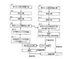
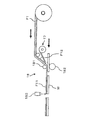
従来の液晶表示装置に実装される光学表示ユニットの製造方法を図11に概念的に示す。まず、光学フィルム製造メーカーでは、光学フィルムを有する帯状シート製品をロール原反として製造する(#1)。この具体的製造工程は公知の製造工程であり、説明は省略する。この帯状シート製品のロール原反として、例えば、液晶表示装置に用いられる偏光板原反、位相差板原反、偏光板と位相差板の積層フィルム原反等がある。次いで、長尺の原反から、貼り合わされる光学表示ユニットのサイズに合わせた形状からなる枚葉のシート製品を打ち抜く(#2)。次いで、打ち抜かれた枚葉のシート製品(光学フィルム)を外観検査する(#3)。この検査方法としては、例えば、目視による欠点検査、公知の欠点検査装置を用いた検査が挙げられる。欠点は、例えば、表面又は内部の汚れ、傷、異物をかみ込んだ打痕状のひねったような特殊状欠点(クニックと称されることがある)、気泡、異物等を意味している。次いで、完成品検査をする(#4)。完成品検査は、外観検査よりも良品判定の厳しい品質基準に従った検査である。次いで、枚葉のシート製品の4方の端面を端面加工する(#5)。これは、輸送中において、端面から粘着剤等がはみださないように防止するために行なわれる。次いで、クリーンルーム環境において、枚葉のシート製品をクリーン包装する(#6)。次いで、輸送のために包装(輸送梱包)する(#7)。以上のようにして枚葉のシート製品が製造され、パネル加工メーカーに輸送される。 A manufacturing method of an optical display unit mounted on a conventional liquid crystal display device is conceptually shown in FIG. First, an optical film manufacturer manufactures a strip-shaped sheet product having an optical film as a roll stock (# 1). This specific manufacturing process is a known manufacturing process and will not be described. Examples of the roll stock of the strip-shaped sheet product include a polarizing plate original used for a liquid crystal display device, a retardation plate original, a laminated film original of a polarizing plate and a retardation plate, and the like. Next, a sheet product having a shape matching the size of the optical display unit to be bonded is punched out of the long original fabric (# 2). Next, the appearance of the punched sheet product (optical film) is inspected (# 3). Examples of the inspection method include visual defect inspection and inspection using a known defect inspection apparatus. The defect means, for example, a surface or internal stain, scratch, a special defect such as a dent in which a foreign object is bitten (sometimes referred to as a knick), a bubble, a foreign object, or the like. Next, the finished product is inspected (# 4). The finished product inspection is an inspection that complies with quality standards that are more stringent than the appearance inspection. Next, end faces of the four end faces of the sheet product are processed (# 5). This is performed to prevent the adhesive or the like from protruding from the end face during transportation. Next, in a clean room environment, the single-sheet product is clean-wrapped (# 6). Next, it is packed for transportation (transport packaging) (# 7). As described above, a sheet product is manufactured and transported to a panel processing manufacturer.
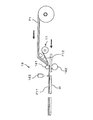
パネル加工メーカーでは、輸送されてきた枚葉のシート製品を梱包解体する(#11)。次いで、輸送中あるいは梱包解体時に生じた傷、汚れ等を検査するために外観検査をする(#12)。検査で良品判定された枚葉のシート製品は、次工程に搬送される。なお、この外観検査を省略する場合もある。枚葉のシート製品が貼り合わされる光学表示ユニット(例えば、液晶セルが封入されたガラス基板ユニット)は、予め製造され、光学表示ユニットは貼り合わせ工程の前に洗浄される(#13)。 The panel processing manufacturer packs and disassembles the sheet product that has been transported (# 11). Next, an appearance inspection is performed in order to inspect for scratches, dirt, etc. that occur during transportation or at the time of unpacking (# 12). The single-sheet product that has been determined to be non-defective in the inspection is conveyed to the next process. Note that this appearance inspection may be omitted. An optical display unit (for example, a glass substrate unit in which a liquid crystal cell is sealed) on which a sheet product is bonded is manufactured in advance, and the optical display unit is cleaned before the bonding process (# 13).
枚葉のシート製品と光学表示ユニットを貼り合わせる(#14)。枚葉のシート製品から粘着剤層を残して離型フィルムが剥離され、粘着剤層を貼り合わせ面として光学表示ユニットの一方の面に貼り合わせる。さらに、光学表示ユニットの他方の面にも同様に貼り合わせることができる。両面に貼り合わせる場合、光学表示ユニットのそれぞれの面には、同一構成の光学フィルムが貼り合わせるように構成されてもよく、異なる構成の光学フィルムが貼り合わされるように構成されていてもよい。次いで、光学フィルムが貼り合わせられた状態の光学表示装置の検査および欠点検査を行なう(#15)。この検査で良品判定された光学表示装置は、実装工程に搬送される(#16)。一方、不良品判定された光学表示装置は、リワーク処理が施される(#17)。リワーク処理で、光学表示ユニットから光学フィルムが剥離される。リワーク処理された光学表示ユニットは、新たに光学フィルムが貼り合わされる(#14)。 The sheet product and the optical display unit are bonded together (# 14). The release film is peeled off from the sheet product leaving the pressure-sensitive adhesive layer, and the pressure-sensitive adhesive layer is bonded to one surface of the optical display unit as a bonding surface. Further, it can be similarly bonded to the other surface of the optical display unit. When bonding to both surfaces, the optical film of the same structure may be bonded to each surface of the optical display unit, or an optical film of a different structure may be bonded. Next, inspection and defect inspection of the optical display device with the optical film bonded are performed (# 15). The optical display device determined to be non-defective in this inspection is transported to the mounting process (# 16). On the other hand, the optical display device determined to be defective is subjected to a rework process (# 17). In the rework process, the optical film is peeled from the optical display unit. An optical film is newly bonded to the reworked optical display unit (# 14).
以上の製造工程において、特に端面加工、枚葉のシート製品の包装、梱包解体等は、光学フィルム製造メーカーとパネル加工メーカーとが別々の場所に存在しているために必要な工程となっている。しかしながら、多工程による製造コストの上昇問題があり、また、多工程や輸送により生じる傷、埃、汚れ等の問題、それに伴う検査工程の必要性、さらに他種類の枚葉シート製品を在庫として保管・管理しなければならないという問題がある。 In the above manufacturing process, end face processing, sheet-sheet product packaging, packaging disassembly, etc. are necessary steps because the optical film manufacturer and the panel processing manufacturer exist in different places. . However, there are problems in increasing manufacturing costs due to multiple processes, problems such as scratches, dust, and dirt caused by multiple processes and transportation, the necessity of inspection processes associated therewith, and storage of other types of single-sheet products as stock.・ There is a problem that it must be managed.
これを解決する方法として、特開2007−140046号公報(特許文献1)が提案されている。この方法によれば、光学表示装置の部材である光学フィルムを有する帯状シート製品が巻き取られたロール原反から帯状シート製品を引き出して供給する供給手段と、供給手段によって引き出された帯状シート製品の欠陥を検出する検出手段と、検出手段の検出結果に基づいて帯状シート製品を切断し、個々のシート製品に加工する切断加工手段と、切断加工手段で切断加工されたシート製品を貼合わせ加工を行うために移送する移送手段と、移送手段によって移送されたシート製品と光学表示装置の部材である光学表示ユニットを貼合わせる貼合わせ加工手段とを具備し、これら各手段を連続した製造ライン工程上に配置したことを特徴とする。上記の構成においては、光学フィルムを有する帯状シート製品から直接、所望のサイズに切断加工して、この切断されたシート製品を光学表示ユニットに貼り合わせることができる。よって、従来であれば、帯状シート製品を打ち抜き、打ち抜き後のシート製品を厳重に梱包し、パネル加工メーカーに納品していたところを、ロール原反に巻き付けた帯状シート製品を直接梱包して納品することが可能となる。 As a method for solving this, Japanese Patent Laid-Open No. 2007-140046 (Patent Document 1) has been proposed. According to this method, the supply means for pulling out and supplying the belt-like sheet product from the roll roll on which the belt-like sheet product having the optical film as a member of the optical display device is wound, and the belt-like sheet product drawn by the supply means The detecting means for detecting defects, the cutting means for cutting the strip-like sheet product based on the detection result of the detecting means, and processing into individual sheet products, and the sheet product cut by the cutting means are bonded together And a transfer means for transferring the sheet product, and a bonding processing means for bonding the sheet product transferred by the transfer means to the optical display unit which is a member of the optical display device. It is arranged above. In said structure, it cuts directly into a desired size from the strip | belt-shaped sheet product which has an optical film, and this cut | disconnected sheet product can be bonded together to an optical display unit. Therefore, in the past, the belt-shaped sheet product was punched out, the punched sheet product was strictly packed, and delivered to the panel processing manufacturer. It becomes possible to do.
また、特開2005−37417号公報(特許文献2)にも、ロール原反から帯状フィルムを引き出して切断し、基板(光学表示ユニットに相当)に貼り合わせる構成が開示されている。 Japanese Patent Laying-Open No. 2005-37417 (Patent Document 2) also discloses a configuration in which a belt-like film is pulled out from a raw roll and cut and bonded to a substrate (corresponding to an optical display unit).
しかしながら、特許文献1の光学表示装置の製造システムでは、光学表示ユニットの一方の片面に光学フィルムを貼り合わせた後、他の片面に光学フィルムを貼り合わせる際の装置を別途備えるものが開示されていない。このため、同一の製造システムを用いて、他の片面に光学フィルムを貼り合わせる場合、貼り合わせ後の光学表示ユニットを装置へローディングする際に二度手間になるなど、製造効率を改善する余地があった。
However, the manufacturing system of the optical display device disclosed in
また、光学表示ユニットの一方表面と他方表面とに貼り合わせる偏光板は、一方表面と他方表面とで吸収軸の方向が異なる(垂直に交差)と共に、ロール幅方向に吸収軸を有するロール原反を製造するのは一般に困難であり、その一方で、通常の光学表示ユニットは長方形を有している。これらを考慮すると、帯状シート製品の供給手段から貼合わせ加工手段までの各手段を、特許文献1の製造システムに追加するのみでは、装置構成が十分とは言えないものであった。
In addition, the polarizing plate to be bonded to the one surface and the other surface of the optical display unit has a roll original fabric in which the absorption axis direction is different (vertically intersects) on the one surface and the other surface, and the absorption axis is in the roll width direction. Is generally difficult to manufacture, while conventional optical display units have a rectangular shape. Considering these, it is not possible to say that the apparatus configuration is sufficient only by adding each means from the supply means for the belt-shaped sheet product to the laminating means to the manufacturing system of
また、偏光板を一方表面と他方表面とに積層する場合に限らず、例えば位相差板を光学表示ユニットの一方表面と他方表面とに積層する場合にも、一方表面と他方表面とで遅相軸の方向を直交させなければならない場合があり、その場合でも偏光板を積層する場合と同様の問題があった。 Further, not only when the polarizing plate is laminated on one surface and the other surface, but also when, for example, a retardation plate is laminated on one surface and the other surface of the optical display unit, the phase is delayed between the one surface and the other surface. In some cases, the directions of the axes have to be orthogonal, and even in that case, there is a problem similar to the case where the polarizing plates are laminated.
特許文献2には、実施形態3として、幅の異なる2つの帯状フィルムをそれぞれロール原反から引き出して切断し、基板の両面に貼り合せる構成が開示されている(段落[0037]〜[0044]及び[図6]〜[図9])。この実施形態3では、2つの帯状フィルムの搬送方向が直交するような配置とされることにより、それらの帯状フィルムから引き出されて切断されたフィルムの軸方向が、基板の両面に貼り合わされた状態で互いに直交するようになっている。しかし、このような構成では、2つの帯状フィルムの搬送方向が直交するような配置とされることにより、製造システムが大型化してしまうという問題がある。
そこで、本発明の目的は、吸収軸等の光学異方性が同じ方向の2つのロール原反を使用して、光学異方性が直交するように光学フィルムを光学表示ユニットの一方表面と他方表面とに貼り合わせることができる光学表示装置の製造システム及び製造方法を提供することにある。 Accordingly, an object of the present invention is to use two rolls having the same optical anisotropy such as an absorption axis in the same direction so that the optical film is perpendicular to the one surface and the other of the optical display unit. An object of the present invention is to provide a manufacturing system and a manufacturing method of an optical display device that can be bonded to a surface.
上記目的は、下記の如き本発明により達成できる。即ち、本発明の光学表示装置の製造システムは、偏光板を含む光学フィルムを長方形の光学表示ユニットに貼り合せた光学表示装置の製造システムであって、光学表示ユニットを供給する光学表示ユニットの供給装置と、第1光学フィルムを有する帯状シート製品が巻き取られたロール原反から帯状シート製品を引き出して供給する第1光学フィルムの供給装置と、前記光学表示ユニットの供給装置から供給された光学表示ユニットの一方表面に、前記第1光学フィルムの供給装置から供給された第1光学フィルムを貼り合せる第1貼合手段、及び、前記第1光学フィルムの供給装置から供給された第1光学フィルムを切断する第1切断手段を含む第1切断貼合装置と、第1光学フィルムの貼り合せ後の光学表示ユニットを搬送して供給する搬送供給装置と、前記第1光学フィルムの偏光板と吸収軸が同じ方向の偏光板を含む第2光学フィルムを有する帯状シート製品が巻き取られたロール原反から帯状シート製品を引き出して供給する第2光学フィルムの供給装置と、前記搬送供給装置から供給された光学表示ユニットの他方表面に、前記第2光学フィルムの供給装置から供給された第2光学フィルムを貼り合せる第2貼合手段、及び、前記第2光学フィルムの供給装置から供給された第2光学フィルムを切断する第2切断手段を含む第2切断貼合装置とを備え、前記第1切断貼合装置および前記第2切断貼合装置は、一方の切断貼合装置が前記光学表示ユニットの短辺に対応する幅の光学フィルムを長辺に対応する長さで切断し、他方の切断貼合装置が前記光学表示ユニットの長辺に対応する幅の光学フィルムを短辺に対応する長さで切断するように構成してあり、前記搬送供給装置は、前記第1切断貼合装置で貼り合せた後の光学表示ユニットを、前記第2切断貼合装置での貼り合せ方向に旋回させる旋回機構を有することを特徴とする。 The above object can be achieved by the present invention as described below. That is, the optical display device manufacturing system of the present invention is an optical display device manufacturing system in which an optical film including a polarizing plate is bonded to a rectangular optical display unit, and the optical display unit supplying the optical display unit is supplied. An apparatus, a first optical film supply device that draws and supplies the belt-shaped sheet product from a roll that is wound with the first optical film, and an optical device that is supplied from the optical display unit supply device. First bonding means for bonding the first optical film supplied from the first optical film supply device to one surface of the display unit, and the first optical film supplied from the first optical film supply device A first cutting and laminating apparatus including a first cutting means for cutting the optical display unit and an optical display unit after bonding of the first optical film are conveyed and supplied. A strip-shaped sheet product is drawn out and supplied from a roll roll on which a strip-shaped sheet product having a second optical film including a polarizing plate having the same absorption axis as the polarizing plate of the first optical film is wound. A second optical film supply device; and a second bonding means for bonding the second optical film supplied from the second optical film supply device to the other surface of the optical display unit supplied from the transport supply device; And a second cutting and bonding device including a second cutting means for cutting the second optical film supplied from the second optical film supply device, the first cutting and bonding device and the second cutting and bonding device. In the combined device, one cutting and bonding apparatus cuts an optical film having a width corresponding to the short side of the optical display unit with a length corresponding to the long side, and the other cutting and bonding apparatus is the optical display unit. The optical film having a width corresponding to the side is configured to be cut by a length corresponding to the short side, and the transport supply device is configured to bond the optical display unit after being bonded by the first cutting and bonding device. It has the turning mechanism made to turn in the bonding direction in the said 2nd cutting bonding apparatus, It is characterized by the above-mentioned.
本発明の光学表示装置の製造システムによると、光学表示ユニットの短辺に対応する幅のロール原反と、長辺に対応する幅のロール原反とを用いることにより、各々から供給される光学フィルムを一定間隔で切断するだけで、光学表示ユニットの短辺及び長辺に対応する光学フィルムを各々得ることができる。このため、前者を長辺に対応する長さに切断して光学表示ユニットの一方表面に貼り合わせ、後者を短辺に対応する長さに切断して光学表示ユニットの他方表面に貼り合わせることによって、吸収軸が同じ方向の2つのロール原反を使用して、吸収軸が直交するように光学表示ユニットの両面に光学フィルムを貼り合わせることができるので、軸精度を向上することができる。 According to the system for manufacturing an optical display device of the present invention, by using a roll original having a width corresponding to the short side of the optical display unit and a roll original having a width corresponding to the long side, the optical supplied from each of them. Optical films corresponding to the short side and the long side of the optical display unit can be obtained by simply cutting the film at regular intervals. For this reason, the former is cut to a length corresponding to the long side and bonded to one surface of the optical display unit, and the latter is cut to a length corresponding to the short side and bonded to the other surface of the optical display unit. Since the optical film can be bonded to both surfaces of the optical display unit so that the absorption axes are orthogonal to each other using two rolls having the same absorption axis, the axial accuracy can be improved.
また、旋回機構を有することによって、第1光学フィルムの搬送方向と第2光学フィルムの搬送方向とが直交するような配置とする必要が無くなり、製造システムの省スペース化を図ることができる。また、旋回機構により第2切断貼合装置における貼り合わせ角度を適正化できる。つまり、光学フィルムのような可とう性の高いものを旋回させるよりも、より硬い光学表示ユニットを旋回させる方が、旋回の位置精度を高めることができる。 Moreover, by having a turning mechanism, it is not necessary to arrange so that the transport direction of the first optical film and the transport direction of the second optical film are orthogonal to each other, and space can be saved in the manufacturing system. Moreover, the bonding angle in a 2nd cutting bonding apparatus can be optimized by a turning mechanism. That is, the turning position accuracy can be increased by turning a harder optical display unit than turning a highly flexible material such as an optical film.
前記第1切断貼合装置は、前記第1貼合手段により第1光学フィルムを光学表示ユニットの一方表面に貼り合せた後に、当該第1光学フィルムを前記第1切断手段により切断し、前記第2切断貼合装置は、前記第2貼合手段により第2光学フィルムを光学表示ユニットの他方表面に貼り合せた後に、当該第2光学フィルムを前記第2切断手段により切断することが好ましい。このような構成によると、光学表示ユニットの短辺に対応する幅の光学フィルムを光学表示ユニットの一方表面に貼り合わせた後に長辺に対応する長さに切断し、光学表示ユニットの長辺に対応する幅の光学フィルムを光学表示ユニットの他方表面に貼り合わせた後に短辺に対応する長さに切断することによって、吸収軸等の光学異方性が同じ方向の2つのロール原反を使用して、光学異方性が直交するように光学フィルムを光学表示ユニットの一方表面と他方表面とに貼り合わせることができる。 The first cutting and bonding apparatus cuts the first optical film by the first cutting means after bonding the first optical film to one surface of the optical display unit by the first bonding means, It is preferable that a 2 cut bonding apparatus cut | disconnects the said 2nd optical film by the said 2nd cutting means, after bonding the 2nd optical film to the other surface of an optical display unit by the said 2nd bonding means. According to such a configuration, an optical film having a width corresponding to the short side of the optical display unit is bonded to one surface of the optical display unit and then cut to a length corresponding to the long side, Two rolls with the same optical anisotropy, such as absorption axis, are used by bonding the optical film of the corresponding width to the other surface of the optical display unit and then cutting it to the length corresponding to the short side. And an optical film can be bonded together to the one surface and the other surface of an optical display unit so that optical anisotropy may orthogonally cross.
また、本発明の光学表示装置の製造システムは、光学異方性を有する光学フィルムを光学表示ユニットに貼り合せた光学表示装置の製造システムであって、前記光学表示ユニットの短辺に対応する幅の第1光学フィルムを有する帯状シート製品が巻き取られたロール原反を用いて、第1光学フィルムを光学表示ユニットの一方表面に貼り合せた後に、前記光学表示ユニットの長辺に対応する長さに第1光学フィルムを切断する第1切断貼合装置と、前記光学表示ユニットの長辺に対応する幅の第2光学フィルムを有する帯状シート製品が巻き取られたロール原反を用いて、第2光学フィルムを光学表示ユニットの他方表面に貼り合せた後に、前記光学表示ユニットの短辺に対応する長さに第2光学フィルムを切断する第2切断貼合装置とを備えることを特徴とする。 The optical display device manufacturing system of the present invention is an optical display device manufacturing system in which an optical film having optical anisotropy is bonded to an optical display unit, and has a width corresponding to the short side of the optical display unit. After the first optical film is bonded to one surface of the optical display unit using the roll raw material on which the belt-like sheet product having the first optical film is wound, the length corresponding to the long side of the optical display unit In addition, by using a roll raw material in which a strip-shaped sheet product having a second optical film having a width corresponding to the long side of the optical display unit is wound, and a first cutting and pasting device that cuts the first optical film, A second cutting and laminating device for cutting the second optical film to a length corresponding to the short side of the optical display unit after the second optical film is bonded to the other surface of the optical display unit; And wherein the Rukoto.
本発明の光学表示装置の製造システムによると、光学表示ユニットの短辺に対応する幅のロール原反と、長辺に対応する幅のロール原反とを用いることにより、各々から供給される光学フィルムを一定間隔で切断するだけで、光学表示ユニットの短辺及び長辺に対応する光学フィルムを各々得ることができる。このため、前者を光学表示ユニットの一方表面に貼り合わせた後に長辺に対応する長さに切断し、後者を光学表示ユニットの他方表面に貼り合わせた後に短辺に対応する長さに切断することによって、吸収軸等の光学異方性が同じ方向の2つのロール原反を使用して、光学異方性が直交するように光学フィルムを光学表示ユニットの一方表面と他方表面とに貼り合わせることができる。 According to the system for manufacturing an optical display device of the present invention, by using a roll original having a width corresponding to the short side of the optical display unit and a roll original having a width corresponding to the long side, the optical supplied from each of them. Optical films corresponding to the short side and the long side of the optical display unit can be obtained by simply cutting the film at regular intervals. For this reason, the former is bonded to one surface of the optical display unit and then cut to a length corresponding to the long side, and the latter is bonded to the other surface of the optical display unit and then cut to a length corresponding to the short side. By using two rolls having the same direction of optical anisotropy such as the absorption axis, the optical film is bonded to one surface and the other surface of the optical display unit so that the optical anisotropy is orthogonal. be able to.
一方、本発明の光学表示装置の製造方法は、偏光板を含む光学フィルムを長方形の光学表示ユニットに貼り合せた光学表示装置の製造方法であって、光学表示ユニットを供給する光学表示ユニットの供給工程と、第1光学フィルムを有する帯状シート製品が巻き取られたロール原反から帯状シート製品を引き出して供給する第1光学フィルムの供給工程と、前記光学表示ユニットの供給工程で供給された光学表示ユニットの一方表面に、前記第1光学フィルムの供給工程で供給された第1光学フィルムを貼り合せる第1貼合工程、及び、前記第1光学フィルムの供給工程で供給された第1光学フィルムを切断する第1切断工程を含む第1切断貼合工程と、第1光学フィルムの貼り合せ後の光学表示ユニットを搬送して供給する搬送供給工程と、前記第1光学フィルムの偏光板と吸収軸が同じ方向の偏光板を含む第2光学フィルムを有する帯状シート製品が巻き取られたロール原反から帯状シート製品を引き出して供給する第2光学フィルムの供給工程と、前記搬送供給工程で供給された光学表示ユニットの他方表面に、前記第2光学フィルムの供給工程で供給された第2光学フィルムを貼り合せる第2貼合工程、及び、前記第2光学フィルムの供給工程で供給された第2光学フィルムを切断する第2切断工程を含む第2切断貼合工程とを備え、前記第1切断貼合工程および前記第2切断貼合工程は、一方の切断貼合工程で前記光学表示ユニットの短辺に対応する幅の光学フィルムを長辺に対応する長さで切断し、他方の切断貼合工程で前記光学表示ユニットの長辺に対応する幅の光学フィルムを短辺に対応する長さで切断するように構成してあり、前記搬送供給工程は、前記第1切断貼合工程で貼り合せた後の光学表示ユニットを、前記第2切断貼合工程での貼り合せ方向に旋回させる旋回工程を有することを特徴とする。 On the other hand, the manufacturing method of the optical display device of the present invention is a manufacturing method of an optical display device in which an optical film including a polarizing plate is bonded to a rectangular optical display unit, and the optical display unit supplying the optical display unit is supplied. A step of supplying a first optical film that is drawn out and supplied from a raw roll from which the belt-like sheet product having the first optical film is wound, and an optical device supplied in the step of supplying the optical display unit A first optical film supplied in the first optical film supply step, and a first optical film supplied in the first optical film supply step, and a first optical film supplied in the first optical film supply step. A first cutting and bonding step including a first cutting step for cutting the sheet, and a conveying and supplying step for conveying and supplying the optical display unit after bonding of the first optical film; A second optical film of which the strip-shaped sheet product is drawn out and supplied from the raw roll on which the strip-shaped sheet product having the second optical film including the polarizing plate having the same absorption axis as the polarizing plate of the first optical film is wound A second bonding step of bonding the second optical film supplied in the supply step of the second optical film to the other surface of the optical display unit supplied in the supply step and the transport supply step; and the second A second cutting and bonding step including a second cutting step for cutting the second optical film supplied in the optical film supplying step, wherein the first cutting and bonding step and the second cutting and bonding step are In the cutting and bonding step, the optical film having a width corresponding to the short side of the optical display unit is cut with a length corresponding to the long side, and in the other cutting and bonding step, the width corresponding to the long side of the optical display unit. Light of It is comprised so that a film may be cut | disconnected by the length corresponding to a short side, and the said conveyance supply process WHEREIN: The optical display unit after bonding by the said 1st cutting bonding process is a said 2nd cutting bonding process. And a turning step of turning in the bonding direction at.
本発明の光学表示装置の製造方法によると、光学表示ユニットの短辺に対応する幅のロール原反と、長辺に対応する幅のロール原反とを用いることにより、各々から供給される光学フィルムを一定間隔で切断するだけで、光学表示ユニットの短辺及び長辺に対応する光学フィルムを各々得ることができる。このため、前者を長辺に対応する長さに切断して光学表示ユニットの一方表面に貼り合わせ、後者を短辺に対応する長さに切断して光学表示ユニットの他方表面に貼り合わせることによって、吸収軸が同じ方向の2つのロール原反を使用して、吸収軸が直交するように光学表示ユニットの両面に光学フィルムを貼り合わせることができるので、軸精度を向上することができる。 According to the method for manufacturing an optical display device of the present invention, by using a roll original having a width corresponding to the short side of the optical display unit and a roll original having a width corresponding to the long side, the optical supplied from each of them. Optical films corresponding to the short side and the long side of the optical display unit can be obtained by simply cutting the film at regular intervals. For this reason, the former is cut to a length corresponding to the long side and bonded to one surface of the optical display unit, and the latter is cut to a length corresponding to the short side and bonded to the other surface of the optical display unit. Since the optical film can be bonded to both surfaces of the optical display unit so that the absorption axes are orthogonal to each other using two rolls having the same absorption axis, the axial accuracy can be improved.
また、旋回工程を有することによって、第1光学フィルムの搬送方向と第2光学フィルムの搬送方向とが直交するような配置とする必要が無くなり、製造システムの省スペース化を図ることができる。また、旋回工程により第2切断貼合工程における貼り合わせ角度を適正化できる。つまり、光学フィルムのような可とう性の高いものを旋回させるよりも、より硬い光学表示ユニットを旋回させる方が、旋回の位置精度を高めることができる。 Moreover, by having a turning process, it becomes unnecessary to arrange | position so that the conveyance direction of a 1st optical film and the conveyance direction of a 2nd optical film may orthogonally cross, and the space-saving of a manufacturing system can be achieved. Moreover, the bonding angle in a 2nd cutting bonding process can be optimized by a turning process. That is, the turning position accuracy can be increased by turning a harder optical display unit than turning a highly flexible material such as an optical film.
前記第1切断貼合工程では、前記第1貼合工程により第1光学フィルムを光学表示ユニットの一方表面に貼り合せた後に、当該第1光学フィルムを前記第1切断工程により切断し、前記第2切断貼合工程では、前記第2貼合工程により第2光学フィルムを光学表示ユニットの他方表面に貼り合せた後に、当該第2光学フィルムを前記第2切断工程により切断することが好ましい。このような構成によると、光学表示ユニットの短辺に対応する幅の光学フィルムを光学表示ユニットの一方表面に貼り合わせた後に長辺に対応する長さに切断し、光学表示ユニットの長辺に対応する幅の光学フィルムを光学表示ユニットの他方表面に貼り合わせた後に短辺に対応する長さに切断することによって、吸収軸等の光学異方性が同じ方向の2つのロール原反を使用して、光学異方性が直交するように光学フィルムを光学表示ユニットの一方表面と他方表面とに貼り合わせることができる。 In the first cutting and bonding step, after the first optical film is bonded to one surface of the optical display unit in the first bonding step, the first optical film is cut by the first cutting step, and the first In the two-cut bonding step, it is preferable that the second optical film is cut by the second cutting step after the second optical film is bonded to the other surface of the optical display unit by the second bonding step. According to such a configuration, an optical film having a width corresponding to the short side of the optical display unit is bonded to one surface of the optical display unit and then cut to a length corresponding to the long side, Two rolls with the same optical anisotropy, such as absorption axis, are used by bonding the optical film of the corresponding width to the other surface of the optical display unit and then cutting it to the length corresponding to the short side. And an optical film can be bonded together to the one surface and the other surface of an optical display unit so that optical anisotropy may orthogonally cross.
また、本発明の光学表示装置の製造方法は、光学異方性を有する光学フィルムを光学表示ユニットに貼り合せた光学表示装置の製造方法であって、前記光学表示ユニットの短辺に対応する幅の第1光学フィルムを有する帯状シート製品が巻き取られたロール原反を用いて、第1光学フィルムを光学表示ユニットの一方表面に貼り合せた後に、前記光学表示ユニットの長辺に対応する長さに第1光学フィルムを切断する第1切断貼合工程と、前記光学表示ユニットの長辺に対応する幅の第2光学フィルムを有する帯状シート製品が巻き取られたロール原反を用いて、第2光学フィルムを光学表示ユニットの他方表面に貼り合せた後に、前記光学表示ユニットの短辺に対応する長さに第2光学フィルムを切断する第2切断貼合工程とを含むことを特徴とする。 The optical display device manufacturing method of the present invention is an optical display device manufacturing method in which an optical film having optical anisotropy is bonded to an optical display unit, and has a width corresponding to the short side of the optical display unit. After the first optical film is bonded to one surface of the optical display unit using the roll raw material on which the belt-like sheet product having the first optical film is wound, the length corresponding to the long side of the optical display unit First, a first cut and pasting step for cutting the first optical film, and a roll raw material on which a belt-shaped sheet product having a second optical film having a width corresponding to the long side of the optical display unit is wound, Including a second cutting and bonding step of cutting the second optical film to a length corresponding to the short side of the optical display unit after the second optical film is bonded to the other surface of the optical display unit. And butterflies.
本発明の光学表示装置の製造方法によると、光学表示ユニットの短辺に対応する幅のロール原反と、長辺に対応する幅のロール原反とを用いて、前者を光学表示ユニットの一方表面に貼り合わせた後に長辺に対応する長さに切断し、後者を光学表示ユニットの他方表面に貼り合わせた後に短辺に対応する長さに切断する。このため、吸収軸等の光学異方性が同じ方向の2つのロール原反を使用して、光学異方性が直交するように光学フィルムを光学表示ユニットの一方表面と他方表面とに貼り合わせることができる。 According to the method for manufacturing an optical display device of the present invention, a former roll of a width corresponding to the short side of the optical display unit and a roll roll of a width corresponding to the long side are used as one of the optical display units. After being bonded to the surface, it is cut to a length corresponding to the long side, and the latter is bonded to the other surface of the optical display unit and then cut to a length corresponding to the short side. For this reason, the optical film is bonded to one surface and the other surface of the optical display unit so that the optical anisotropy is orthogonal using two rolls having the same optical anisotropy such as an absorption axis. be able to.
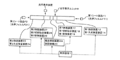
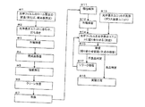
以下、本発明の実施形態について、光学表示装置の製造システムに用いる原材料、製造工程の流れ、製造システムの各部の構成の順で説明する。図1に、光学表示装置の製造方法のフローチャートの一例を示す。図2に、光学表示装置の製造システムの一例の構成図を示す。図3に、光学表示装置の製造システムの一例の平面配置図を示す。 Hereinafter, embodiments of the present invention will be described in the order of raw materials used in a manufacturing system of an optical display device, a flow of a manufacturing process, and a configuration of each part of the manufacturing system. FIG. 1 shows an example of a flowchart of a method for manufacturing an optical display device. FIG. 2 shows a configuration diagram of an example of an optical display device manufacturing system. FIG. 3 shows a plan layout view of an example of a manufacturing system for an optical display device.
(光学表示ユニット)
本発明に用いられる光学表示ユニットは、文字や画像を表示するための一まとまりの部品をいう。上記光学表示ユニットは、例えば液晶セルや有機エレクトロルミネッセンスパネル等である。本発明は、長方形の外形を有する光学表示ユニットに有効であり、例えば、長辺/短辺が16/9であるものや、4/3であるものなどが用いられる。なお、光学表示ユニットとしては、予め、光学フィルム等の部材が積層一体化されたものであってもよい。
(Optical display unit)
The optical display unit used in the present invention refers to a group of parts for displaying characters and images. The optical display unit is, for example, a liquid crystal cell or an organic electroluminescence panel. The present invention is effective for an optical display unit having a rectangular outer shape, and for example, one having a long side / short side of 16/9 or 4/3 is used. In addition, as an optical display unit, members, such as an optical film, may be previously laminated and integrated.
(光学フィルム)
光学表示ユニットに貼り付けられる光学フィルムは、単層であっても複層であってもよい。上記光学フィルムは、少なくともその一層に光学異方性を有する。上記光学異方性とは、光学的性質が面内で異なることをいい、具体的には、吸収異方性、屈折率異方性、反射異方性等である。上記光学フィルムは、例えば、吸収軸を有する偏光板や、遅相軸を有する位相差フィルム、透過軸を有する輝度向上フィルム、又はこれらの積層体である。
(Optical film)
The optical film attached to the optical display unit may be a single layer or a multilayer. The optical film has optical anisotropy in at least one layer thereof. The optical anisotropy means that optical properties are different in a plane, and specifically, an absorption anisotropy, a refractive index anisotropy, a reflection anisotropy, and the like. The optical film is, for example, a polarizing plate having an absorption axis, a retardation film having a slow axis, a brightness enhancement film having a transmission axis, or a laminate thereof.
本発明に用いられる帯状シート製品は、上記光学表示ユニットの短辺又は長辺に対応する幅に加工された、幅方向よりも長手方向が十分に長いシートをいう。上記帯状シート製品の長さは、例えば幅の10倍以上である。上記帯状シート製品は、上記光学フィルムを含むものであれば特に制限はない。上記帯状シート製品は、好ましくは、偏光板を含む光学フィルム、粘着剤層、及び離型フィルムをこの順に有する。 The strip-shaped sheet product used in the present invention refers to a sheet processed in a width corresponding to the short side or the long side of the optical display unit and having a sufficiently longer longitudinal direction than the width direction. The length of the strip-shaped sheet product is, for example, 10 times or more the width. If the said strip | belt-shaped sheet product contains the said optical film, there will be no restriction | limiting in particular. The strip-shaped sheet product preferably has an optical film including a polarizing plate, an adhesive layer, and a release film in this order.
本発明に用いられるロール原反は、上記帯状シート製品をロール状に巻き回したものである。上記ロール原反は、通常、上記帯状シート製品をその一端からロール芯に巻き回して得られる。 The roll stock used in the present invention is a roll of the above-described strip-shaped sheet product. The roll material is usually obtained by winding the belt-like sheet product from one end thereof onto a roll core.
前記偏光板を含む光学フィルムとしては、偏光板、又は偏光板に位相差フィルム、輝度向上フィルム、それらフィルムの2以上の組み合わせを積層した光学フィルム等が例示される。 Examples of the optical film including the polarizing plate include a polarizing plate, an optical film obtained by laminating a retardation film, a brightness enhancement film, and a combination of two or more of these films on the polarizing plate.
これら光学フィルムの表面には、保護用の透明フィルムが積層される場合がある。また、光学フィルムの一方表面には、例えば光学表示ユニットに貼り付けられるように、粘着剤層が形成されるのが好ましく、この粘着剤層を保護するための離型フィルムが設けられる。また、光学フィルムのその他方表面には、例えば粘着剤層を介して表面保護フィルムが設けられる。 A protective transparent film may be laminated on the surface of these optical films. Moreover, it is preferable that an adhesive layer is formed on one surface of the optical film so as to be attached to, for example, an optical display unit, and a release film for protecting the adhesive layer is provided. Moreover, a surface protective film is provided on the other surface of the optical film, for example, via an adhesive layer.
本発明は、光学異方性が同じ方向の2つのロール原反を使用する場合に有効であり、特に、光学フィルムを構成する偏光板の吸収軸が、同じ方向の2つのロール原反を使用する場合に有効である。偏光板の吸収軸の方向は、通常、ロール原反の長尺方向となる。また、位相差フィルムの場合、遅相軸がロール原反の長尺方向と一致するもの、垂直になるもの、一定角度の斜め方向になるもの等がある。以下において、表面保護フィルムおよび離型フィルムが積層された光学フィルムをシート製品と称することがある。 The present invention is effective when two rolls having the same optical anisotropy are used, and in particular, two rolls having the same absorption direction of the polarizing plate constituting the optical film are used. It is effective when The direction of the absorption axis of the polarizing plate is usually the long direction of the roll. Further, in the case of a retardation film, there are those in which the slow axis coincides with the long direction of the roll original fabric, those in which the slow axis is vertical, and those in which the slow axis is in an oblique direction with a constant angle. Hereinafter, an optical film in which a surface protective film and a release film are laminated may be referred to as a sheet product.
ロール原反を構成している長尺の偏光板は、長手方向に延伸されることにより、長手方向に平行な吸収軸を有することが好ましい。このように、長手方向に平行な吸収軸を有する偏光板を用いることにより、光学表示ユニットに貼り合わせる際の軸精度が向上し、貼り合わせ後の光学表示装置の光学特性が良好になる。 The long polarizing plate constituting the raw roll is preferably stretched in the longitudinal direction to have an absorption axis parallel to the longitudinal direction. Thus, by using a polarizing plate having an absorption axis parallel to the longitudinal direction, the axial accuracy when bonded to the optical display unit is improved, and the optical characteristics of the optical display device after bonding are improved.
(製造フローチャート)
本発明の光学表示装置の製造方法は、光学異方性を有する光学フィルムを光学表示ユニットに貼り合せた光学表示装置の製造方法であり、好ましくは、偏光板を含む光学フィルムを光学表示ユニットに貼り合せた光学表示装置の製造方法である。
(Manufacturing flowchart)
The method for producing an optical display device of the present invention is a method for producing an optical display device in which an optical film having optical anisotropy is bonded to an optical display unit. Preferably, an optical film including a polarizing plate is used as the optical display unit. It is a manufacturing method of the bonded optical display device.
本発明の製造方法は、第1切断貼合工程と第2切断貼合工程とを含むものであるが、何れの工程を先に行ってもよく、両工程を同時又はほぼ同時に行ってもよい。 Although the manufacturing method of this invention includes a 1st cutting bonding process and a 2nd cutting bonding process, any process may be performed previously and both processes may be performed simultaneously or substantially simultaneously.
第1切断貼合工程は、前記光学表示ユニットの短辺に対応する幅の第1光学フィルムを有する帯状シート製品が巻き取られたロール原反を用いて、第1光学フィルムを光学表示ユニットの一方表面に貼り合せた後に、前記光学表示ユニットの長辺に対応する長さに切断するものであってもよいし、第1光学フィルムを光学表示ユニットの長辺に対応する長さに切断した後に、前記光学表示ユニットの一方表面に貼り合せるものであってもよい。 A 1st cutting bonding process uses a roll original fabric in which the strip | belt-shaped sheet product which has the 1st optical film of the width | variety corresponding to the short side of the said optical display unit was wound up, and a 1st optical film was used as an optical display unit. On the other hand, after being bonded to the surface, it may be cut to a length corresponding to the long side of the optical display unit, or the first optical film is cut to a length corresponding to the long side of the optical display unit. Later, it may be bonded to one surface of the optical display unit.
第2切断貼合工程は、前記光学表示ユニットの長辺に対応する幅の第2光学フィルムを有する帯状シート製品が巻き取られたロール原反を用いて、第2光学フィルムを光学表示ユニットの他方表面に貼り合せた後に、前記光学表示ユニットの短辺に対応する長さに切断するものであってもよいし、第2光学フィルムを光学表示ユニットの短辺に対応する長さに切断した後に、前記光学表示ユニットの他方表面に貼り合せるものであってもよい。 In the second cutting and bonding step, the second optical film is removed from the optical display unit by using a roll raw material on which a belt-shaped sheet product having a second optical film having a width corresponding to the long side of the optical display unit is wound. After being bonded to the other surface, it may be cut to a length corresponding to the short side of the optical display unit, or the second optical film is cut to a length corresponding to the short side of the optical display unit. Later, it may be bonded to the other surface of the optical display unit.
本実施形態における光学表示装置の製造方法は、より具体的には、例えば第1光学フィルムを有する帯状シート製品が巻き取られたロール原反から帯状シート製品を引き出して供給しながら、前記光学表示ユニットの一方表面に第1光学フィルムを貼り合せた後に、当該第1光学フィルムを所定の長さに切断する第1切断貼合工程と、第2光学フィルムを有する帯状シート製品が巻き取られたロール原反から帯状シート製品を引き出して供給しながら、前記光学表示ユニットの他方表面に第2光学フィルムを貼り合せた後に、当該第2光学フィルムを所定の長さに切断する第2切断貼合工程とを含む。 More specifically, the manufacturing method of the optical display device in the present embodiment is, for example, the optical display while pulling out and supplying the belt-like sheet product from the roll raw material on which the belt-like sheet product having the first optical film is wound. After laminating the first optical film on one surface of the unit, the first cut and pasting step of cutting the first optical film into a predetermined length and the belt-like sheet product having the second optical film were wound up. Second cutting and bonding, in which a second optical film is bonded to the other surface of the optical display unit and then the second optical film is cut to a predetermined length while the strip-shaped sheet product is pulled out and supplied from the roll. Process.
第1切断貼合工程は、例えば、以下で述べる(2)搬送工程〜(4)第1光学フィルム切断貼合工程によって実施され、第2切断貼合工程は、例えば、以下で述べる(7)搬送工程〜(9)第2光学フィルム切断貼合工程によって実施される。 A 1st cutting bonding process is implemented by the (2) conveyance process-(4) 1st optical film cutting bonding process described below, for example, and the 2nd cutting bonding process describes below (7), for example. Carrying step to (9) The second optical film cutting and bonding step is performed.
(1)第1ロール原反準備工程(図1、S1)。第1帯状シート製品を第1ロール原反として準備する。第1ロール原反の幅は、光学表示ユニットの貼り合わせサイズに依存している。具体的には、光学表示ユニットの長辺又は短辺の一方に対応させて、第1ロール原反の幅が決定され、他方に対応させて、第2ロール原反の幅が決定される。このため、第1ロール原反と第2ロール原反とは、異なる幅を有しており、スリット前ロール原反からスリット加工により、予め所定の幅にスリットされたものが使用される。 (1) 1st roll original fabric preparation process (FIG. 1, S1). A 1st strip | belt-shaped sheet product is prepared as a 1st roll original fabric. The width | variety of a 1st roll original fabric is dependent on the bonding size of an optical display unit. Specifically, the width of the first roll original fabric is determined corresponding to one of the long side or the short side of the optical display unit, and the width of the second roll original fabric is determined corresponding to the other side. For this reason, the 1st roll original fabric and the 2nd roll original fabric have different widths, and those previously slit into a predetermined width by slit processing from the roll original fabric before slit are used.
スリット前ロール原反を構成している長尺の偏光板は、長手方向に延伸されることにより、長手方向に平行な吸収軸を有することが好ましい。この場合、スリット前ロール原反から引き出される長尺原反を長手方向に平行にスリット加工し、スリット加工により得られた帯状シート製品をロール状に巻回してロール原反を製造することが好ましい。これにより、ロール原反から帯状シート製品を引き出して光学表示ユニットに貼り合わせる際の軸精度が向上し、貼り合わせ後の光学表示装置の光学特性が良好になる。スリット加工は、スリット前ロール原反を巻き戻しながら行い、その方法としては、レーザ切断装置、回転丸刃等の刃物を用いる方法などが挙げられる。ただし、上記長尺原反は、ロール状のスリット前ロール原反から引き出される構成に限らず、例えば連続的に製造される長尺原反が、そのまま長手方向に平行にスリット加工され、スリット加工により得られた帯状シート製品がロール状に巻回されることにより、ロール原反が製造されるような構成であってもよい。また、スリット前ロール原反を巻き戻さずに、ロール端面の1端面又は両端面を切断する方法も用いることができる。 It is preferable that the long polarizing plate constituting the roll raw material before slit has an absorption axis parallel to the longitudinal direction by being stretched in the longitudinal direction. In this case, it is preferable to produce a raw roll by slitting a long roll drawn from the roll roll before slit in parallel with the longitudinal direction and winding the strip-shaped sheet product obtained by the slit machining into a roll. . Thereby, the axial accuracy at the time of pulling out a strip-shaped sheet product from a roll original fabric and bonding it to an optical display unit is improved, and the optical characteristics of the optical display device after bonding are improved. The slit processing is performed while rewinding the roll material before slit, and examples of the method include a method using a cutting tool such as a laser cutting device or a rotating round blade. However, the above-described long original fabric is not limited to the configuration drawn from the roll-form slit raw material before slitting. For example, a continuously manufactured long original fabric is slit as it is in parallel with the longitudinal direction, and slit processing is performed. The roll sheet may be manufactured by winding the belt-shaped sheet product obtained in the above manner into a roll shape. Moreover, the method of cut | disconnecting one end surface or both end surfaces of a roll end surface, without unwinding the roll raw material before slit can also be used.
本発明において、「光学表示ユニットの長辺又は短辺に対応させる」とは、光学表示ユニットの長辺又は短辺の長さに対応する光学フィルムの貼り合わせの長さ(露出部分を除いた長さ)を指し、光学表示ユニットの長辺又は短辺の長さと光学フィルムの幅とが同じである必要はない。 In the present invention, “corresponding to the long side or short side of the optical display unit” means the length of the optical film bonded to the long side or short side of the optical display unit (excluding the exposed portion). The length of the long side or the short side of the optical display unit and the width of the optical film do not have to be the same.
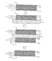
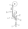
図4に示すように、例えば、第1シート製品F1の積層構造は、第1光学フィルムF11と、第1離型フィルムF12と、表面保護フィルムF13とを有する。第1光学フィルムF11は、第1偏光子F11aと、その一方面に接着剤層(不図示)を介した第1フィルムF11bと、その他方面に接着剤層(不図示)を介した第2フィルムF11cとで構成されている。 As shown in FIG. 4, for example, the laminated structure of the first sheet product F1 includes a first optical film F11, a first release film F12, and a surface protective film F13. The first optical film F11 includes a first polarizer F11a, a first film F11b having an adhesive layer (not shown) on one side thereof, and a second film having an adhesive layer (not shown) on the other side. F11c.
第1、第2フィルムF11b、F11cは、例えば、偏光子保護フィルム(例えばトリアセチルセルロースフィルム、PETフィルム等)である。第2フィルムF11cは、第1粘着剤層F14を介して光学表示ユニットW面側に貼り合わされる。第1フィルムF11bには、表面処理を施すことができる。表面処理としては、例えば、ハードコート処理や反射防止処理、スティッキングの防止や拡散ないしアンチグレア等を目的とした処理等が挙げられる。第1離型フィルムF12は、第2フィルムF11cと第1粘着剤層F14を介して設けられている。また、表面保護フィルムF13は、第1フィルムF11bと粘着剤層F15を介して設けられている。以下において、偏光子と偏光子保護フィルムとの積層構造を偏光板と称することがある。 The first and second films F11b and F11c are, for example, polarizer protective films (for example, triacetyl cellulose film, PET film, etc.). The second film F11c is bonded to the optical display unit W surface side via the first pressure-sensitive adhesive layer F14. A surface treatment can be applied to the first film F11b. Examples of the surface treatment include a hard coat treatment, an antireflection treatment, a treatment for the purpose of prevention of sticking, diffusion or antiglare, and the like. The first release film F12 is provided via the second film F11c and the first pressure-sensitive adhesive layer F14. Moreover, the surface protection film F13 is provided through the 1st film F11b and the adhesive layer F15. Below, the laminated structure of a polarizer and a polarizer protective film may be called a polarizing plate.
以下の各工程は、工場内において隔離された隔離構造内において行なわれ、清浄度が維持されているのが好ましい。特に光学フィルムを光学表示ユニットに貼り合わせる切断貼合工程において清浄度が維持されていることが好ましい。 Each of the following steps is preferably performed in an isolated structure isolated in a factory, and the cleanliness is preferably maintained. In particular, it is preferable that the cleanliness is maintained in the cutting and bonding step of bonding the optical film to the optical display unit.
(2)搬送工程(図1、S2)。準備され設置された第1ロール原反から第1シート製品F1を繰り出し、下流側に搬送する。第1シート製品F1を搬送する第1搬送装置12は、例えば、ニップローラ対、テンションローラ、回転駆動装置、アキュムレート装置、センサー装置、制御装置等で構成されている。
(2) Transport process (FIG. 1, S2). The first sheet material F1 is fed out from the first roll stock prepared and installed, and is conveyed downstream. The first conveying
(3)第1検査工程(図1、S3)。第1シート製品F1の欠点を第1欠点検査装置14を用いて検査する。ここでの欠点検査方法としては、第1シート製品F1の両面に対し、透過光、反射光による画像撮影・画像処理する方法、検査用偏光フィルムをCCDカメラと検査対象物との間に、検査対象である偏光板の偏光軸とクロスニコルとなるように配置(0度クロスと称することがある)して画像撮影・画像処理する方法、検査用偏光フィルムをCCDカメラと検査対象物との間に、検査対象である偏光板の偏光軸と所定角度(例えば、0度より大きく10度以内の範囲)になるように配置(x度クロスと称することがある)して画像撮影・画像処理する方法が挙げられる。なお、画像処理のアルゴリズムは公知の方法を適用でき、例えば二値化処理による濃淡判定によって欠点を検出することができる。
(3) First inspection step (FIG. 1, S3). The first sheet product F1 is inspected for defects using the first
透過光による画像撮影・画像処理方法では、第1シート製品F1内部の異物が検出できる。反射光による画像撮影・画像処理方法では、第1シート製品F1表面の付着異物が検出できる。0度クロスによる画像撮影・画像処理方法では、主に、表面異物、汚れ、内部の異物等が輝点として検出できる。x度クロスによる画像撮影・画像処理方法では、主に、クニックを検出することができる。 In the image capturing / image processing method using transmitted light, foreign matter inside the first sheet product F1 can be detected. In the image photographing / image processing method using the reflected light, the adhered foreign matter on the surface of the first sheet product F1 can be detected. In the image photographing / image processing method using the 0-degree cross, mainly surface foreign matter, dirt, internal foreign matter, etc. can be detected as bright spots. In the image photographing / image processing method using the x-degree cross, a nick can be mainly detected.
第1欠点検査装置14で得られた欠点の情報は、その位置情報(例えば、位置座標)とともに紐付けされて、制御装置1に送信され、後述する第1切断貼合装置18による処理に寄与させることができる。
The defect information obtained by the first
(4)第1光学フィルム切断貼合工程(図1、S4)。第1剥離装置17を用いて第1離型フィルムF12を除去しながら、第1切断貼合装置18を用いて、当該第1離型フィルムF12が除去された第1光学フィルムF11を第1粘着剤層F14を介して光学表示ユニットWに貼り合せた後、第1光学フィルムF11を切断する。貼り合せに際し、後述するように、第1光学フィルムF11と光学表示ユニットWをロール対で挟んで圧着する。貼り合せの際には、第1欠点検査装置14で得られた欠点の情報に基づいて、第1光学フィルムF11における光学表示ユニットWに貼り合わせられる領域内に欠点を含まないように、欠点を避けて貼り合せるように構成される。これにより、第1シート製品F1の歩留まりが大幅に向上する。このような貼り合せの際に用いる欠点情報は、インラインの欠点検査装置で得られたものでも、予めロール原反に付されたものでもよい。
(4) First optical film cutting and pasting step (FIG. 1, S4). While removing the 1st release film F12 using the
第1切断貼合装置18は、表面保護フィルムF13、粘着剤層F15、第1光学フィルムF11および第1粘着剤層F14を切断する切断手段を有する。切断長さに関しては、例えば、光学表示ユニットの長辺又は短辺の一方に対応させて、第1ロール原反の幅が短辺に対応する場合には、光学フィルムを長辺に対応する長さで切断し、または第1ロール原反の幅が長辺に対応する場合には、光学フィルムを短辺に対応する長さで切断する。本実施形態では、図3に示すように、第1ロール原反(第1シート製品F1)の幅が、光学表示ユニットWの短辺に対応する場合の例を示す。
The 1st
切断手段としては、例えば、レーザ装置、カッター、その他の公知の切断手段等が挙げられる。隣接する光学表示ユニットW間で切断され、光学表示ユニットWに貼り合せられなかった部分の第1シート製品F1は、後述する第1排除装置19によって排除される。 Examples of the cutting means include a laser device, a cutter, and other known cutting means. A portion of the first sheet product F1 that is cut between the adjacent optical display units W and is not bonded to the optical display unit W is excluded by a first rejection device 19 described later.
(5−1)洗浄工程(図1、S5−1)。光学表示ユニットWは、研磨洗浄、水洗浄等によって、その表面が洗浄される。洗浄された光学表示ユニットWは、検査装置まで搬送される。 (5-1) Cleaning step (FIG. 1, S5-1). The surface of the optical display unit W is cleaned by polishing cleaning, water cleaning, or the like. The cleaned optical display unit W is transported to the inspection apparatus.
(5−2)検査工程(図1、S5−2)。洗浄後の光学表示ユニットWは、検査装置によって、その表面が検査される。検査後の光学表示ユニットWは、第1切断貼合装置18まで搬送される。
(5-2) Inspection process (FIG. 1, S5-2). The surface of the cleaned optical display unit W is inspected by an inspection device. The optical display unit W after the inspection is conveyed to the first cutting and
これら、第1ロール原反準備工程、第1検査工程、第1光学フィルム切断貼合工程、洗浄工程、検査工程のそれぞれの工程は連続した製造ラインで実行されることが好ましい。以上の一連の製造工程において、光学表示ユニットWの一方面に第1光学フィルムF11が貼り合わされる。以下では、その他面に第2光学フィルムF21を貼り合わる製造工程について説明する。 It is preferable that each process of these 1st roll original fabric preparation processes, a 1st inspection process, a 1st optical film cutting | lamination bonding process, a washing | cleaning process, and an inspection process is performed with the continuous production line. In the above series of manufacturing steps, the first optical film F11 is bonded to one surface of the optical display unit W. Below, the manufacturing process which bonds the 2nd optical film F21 on another surface is demonstrated.
(6)第2ロール原反準備工程(図1、S11)。第2帯状シート製品F2を第2ロール原反として準備する。図4の示すように、第2シート製品F2の積層構造は、第1シート製品と同様の構成であるが、これに限定されない。第2シート製品F2は、第2光学フィルムF21と、第2離型フィルムF22と、表面保護フィルムF23とを有する。第2光学フィルムF21は、第2偏光子21aと、その一方面に接着剤層(不図示)を介した第3フィルムF21bと、その他方面に接着剤層(不図示)を介した第4フィルムF21cとで構成されている。 (6) 2nd roll original fabric preparation process (FIG. 1, S11). A second strip sheet product F2 is prepared as a second roll. As shown in FIG. 4, the laminated structure of the second sheet product F2 has the same configuration as that of the first sheet product, but is not limited thereto. The second sheet product F2 includes a second optical film F21, a second release film F22, and a surface protection film F23. The second optical film F21 includes a second polarizer 21a, a third film F21b having an adhesive layer (not shown) on one side thereof, and a fourth film having an adhesive layer (not shown) on the other side. F21c.
第3、第4フィルムF21b、F21cは、例えば、偏光子保護フィルム(例えばトリアセチルセルロースフィルム。PETフィルム等)である。第4フィルムF21cは、第2粘着剤層F24を介して光学表示ユニットW面側に貼り合わされる。第3フィルムF21bには、表面処理を施すことができる。表面処理としては、例えば、ハードコート処理や反射防止処理、スティッキングの防止や拡散ないしアンチグレア等を目的とした処理等が挙げられる。第2離型フィルムF22は、第4フィルムF21cと第2粘着剤層F24を介して設けられている。また、表面保護フィルムF23は、第3フィルムF21bと粘着剤層F25を介して設けられている。 The third and fourth films F21b and F21c are, for example, polarizer protective films (for example, triacetylcellulose film, PET film, etc.). The fourth film F21c is bonded to the optical display unit W surface side via the second pressure-sensitive adhesive layer F24. The third film F21b can be subjected to a surface treatment. Examples of the surface treatment include a hard coat treatment, an antireflection treatment, a treatment for the purpose of prevention of sticking, diffusion or antiglare, and the like. The second release film F22 is provided via the fourth film F21c and the second pressure-sensitive adhesive layer F24. Moreover, the surface protection film F23 is provided through the 3rd film F21b and the adhesive layer F25.
(7)搬送工程(図1、S12)。準備され設置された第2ロール原反から第2シート製品F2を繰り出し、下流側に搬送する。第2シート製品を搬送する第2搬送装置22は、例えば、ニップローラ対、テンションローラ、回転駆動装置、アキュムレート装置、センサー装置、制御装置等で構成されている。
(7) Transport process (FIG. 1, S12). The second sheet material F2 is fed out from the prepared and installed second roll, and is conveyed downstream. The second conveying
(8)第2検査工程(図1、S13)。第2シート製品F2の欠点を第2欠点検査装置24を用いて検査する。ここでの欠点検査方法は、上述した第1欠点検査装置による方法と同様である。
(8) 2nd inspection process (FIG. 1, S13). The second sheet material F2 is inspected for defects using the second
(9)第2光学フィルム切断貼合工程(図1、S14)。次いで、第2剥離装置27を用いて第2離型フィルムF22を除去しながら、第2切断貼合装置28を用いて、当該第2離型フィルムF22が除去された第2光学フィルムF21を、第2粘着剤層F24を介して、光学表示ユニットWの第1光学フィルムF11が貼り合わされている面と異なる面に貼り合せた後、第2光学フィルムF21を切断する。貼り合せの際には、第2欠点検査装置24で得られた欠点の情報に基づいて、第2光学フィルムF21における光学表示ユニットWに貼り合わせられる領域内に欠点を含まないように、欠点を避けて貼り合せるように構成される。これにより、第2シート製品F2の歩留まりが大幅に向上する。このような貼り合せの際に用いる欠点情報は、インラインの欠点検査装置で得られたものでも、予めロール原反に付されたものでもよい。なお、第2光学フィルムF21を光学表示ユニットWに貼り合せる前に、搬送機構の搬送方向切り替え機構によって光学表示ユニットWを90度回転させ、第1光学フィルムF11と第2光学フィルムF21をクロスニコルの関係にする場合がある。
(9) Second optical film cutting and pasting step (FIG. 1, S14). Then, while removing the second release film F22 using the second peeling device 27, the second optical film F21 from which the second release film F22 has been removed using the second cutting and
つまり、本発明では、第1光学フィルム切断貼合工程で貼り合せた後の光学表示ユニットWを、第2光学フィルム切断貼合工程での貼り合せ方向に旋回させる(上下反転及び回転した状態とすることを含む)旋回工程を含むことが好ましい。本発明では、旋回後の光学表示ユニットWに貼り合わされた第1光学フィルムF11の長辺の方向と、その光学表示ユニットWに貼り合わされる第2光学フィルムF21の長辺の方向とが、0±5°、好ましくは0±1°になるような角度で旋回工程を行うことが好ましい。例えば、供給される第1光学フィルムF11のライン方向と、供給される第2光学フィルムF21のライン方向とが平行(直線上も含む)である場合、旋回工程における旋回角度は、85〜95°が好ましい。貼り合せに際しては、後述するように、第2光学フィルムF21と光学表示ユニットWをロールで挟んで圧着する。 In other words, in the present invention, the optical display unit W after being bonded in the first optical film cutting and bonding step is swung in the bonding direction in the second optical film cutting and bonding step (upside down and rotated) It is preferable to include a turning step. In the present invention, the direction of the long side of the first optical film F11 bonded to the optical display unit W after turning and the direction of the long side of the second optical film F21 bonded to the optical display unit W are 0. It is preferable to perform the turning step at an angle of ± 5 °, preferably 0 ± 1 °. For example, when the line direction of the supplied first optical film F11 and the line direction of the supplied second optical film F21 are parallel (including a straight line), the turning angle in the turning step is 85 to 95 °. Is preferred. At the time of bonding, as will be described later, the second optical film F21 and the optical display unit W are sandwiched between rolls and are bonded.
第2切断貼合装置28は、表面保護フィルムF23、粘着剤層F25、第2光学フィルムF21および第2粘着剤層F24を切断する切断手段を有する。具体的には、光学表示ユニットの長辺又は短辺の一方に対応させて、第2ロール原反の幅が短辺に対応する場合には、光学フィルムを長辺に対応する長さで切断し、または第2ロール原反の幅が長辺に対応する場合には、光学フィルムを短辺に対応する長さで切断する。本実施形態では、図3に示すように、第2ロール原反(第2シート製品F2)の幅が、光学表示ユニットWの長辺に対応する場合の例を示す。
The 2nd
切断手段としては、例えば、レーザ装置、カッター、その他の公知の切断手段等が挙げられる。隣接する光学表示ユニットW間で切断され、光学表示ユニットWに貼り合せられなかった部分の第2シート製品F2は、後述する第2排除装置29によって排除される。 Examples of the cutting means include a laser device, a cutter, and other known cutting means. A portion of the second sheet product F2 that is cut between the adjacent optical display units W and is not bonded to the optical display unit W is excluded by a second rejection device 29 described later.
(10)光学表示装置の検査工程(図1、S15)。検査装置は、光学表示ユニットWの両面に光学フィルムが貼着された光学表示装置を検査する。検査方法としては、光学表示装置の両面に対し、反射光による画像撮影・画像処理する方法が例示される。また他の方法として、検査用偏光フィルムをCCDカメラと検査対象物との間に設置する方法も例示される。なお、画像処理のアルゴリズムは公知の方法を適用でき、例えば二値化処理による濃淡判定によって欠点を検出することができる。 (10) Inspection step of optical display device (FIG. 1, S15). The inspection device inspects the optical display device in which the optical film is attached to both surfaces of the optical display unit W. Examples of the inspection method include a method of taking an image and processing an image using reflected light on both sides of the optical display device. As another method, a method of installing a polarizing film for inspection between the CCD camera and the inspection object is also exemplified. Note that a known method can be applied to the image processing algorithm, and for example, a defect can be detected by density determination by binarization processing.
(11)検査装置で得られた欠点の情報に基づいて、光学表示装置の良品判定がなされる。良品判定された光学表示装置は、次の実装工程に搬送される。不良品判定された場合、リワーク処理が施され、新たに光学フィルムが貼られ、次いで検査され、良品判定の場合、実装工程に移行し、不良品判定の場合、再度リワーク処理に移行するかあるいは廃棄処分される。 (11) A non-defective product of the optical display device is determined based on the defect information obtained by the inspection device. The optical display device determined to be non-defective is conveyed to the next mounting process. If a defective product is determined, a rework process is performed, a new optical film is applied, and then inspected.If a good product is determined, the process proceeds to a mounting process. Discarded.
以上の一連の製造工程において、第1光学フィルムF11の切断貼合工程と第2光学フィルムF21の切断貼合工程とを連続した製造ラインで実行することによって、光学表示装置を好適に製造することができる。 In the above series of manufacturing steps, the optical display device is suitably manufactured by executing the cutting and bonding step of the first optical film F11 and the cutting and bonding step of the second optical film F21 on a continuous production line. Can do.
(欠点を避けた貼合方法の別実施形態)
また、上記第1光学フィルム切断貼合工程および第2光学フィルム切断貼合工程の別実施形態を以下に説明する。この実施形態は、上記の第1検査工程、第2検査工程を備えていない場合に特に有効である。第1および第2ロール原反の幅方向の一方の端部には、所定ピッチ単位(例えば1000mm)に第1、第2シート製品の欠点情報(欠点座標、欠点の種類、サイズ等)がコード情報(例えばQRコード、バーコード)として付されている場合がある。このような場合、光学フィルムを貼り合せる前段階で、このコード情報を読み取り、解析して欠点部分を避けるように、第1、第2光学フィルム切断貼合工程において光学フィルムを光学表示ユニットに貼り合せる。そして、欠点を含む部分は排除あるいは光学表示ユニットではない部材に貼り合わせるように構成し、光学表示ユニットに貼り合せられた部分が良品判定の枚葉のシート製品となるように構成する。これにより、光学フィルムF11,F21の歩留まりが大幅に向上される。
(Another embodiment of the bonding method avoiding the drawbacks)
In addition, another embodiment of the first optical film cutting and bonding step and the second optical film cutting and bonding step will be described below. This embodiment is particularly effective when the first inspection process and the second inspection process are not provided. At one end in the width direction of the first and second rolls, defect information (defect coordinates, defect type, size, etc.) of the first and second sheet products is coded in a predetermined pitch unit (for example, 1000 mm). It may be attached as information (for example, QR code, barcode). In such a case, the optical film is pasted on the optical display unit in the first and second optical film cutting and pasting processes so that the code information is read and analyzed before the optical film is pasted to avoid the defective part. Match. The part including the defect is excluded or configured to be bonded to a member that is not an optical display unit, and the part bonded to the optical display unit is configured to be a non-defective sheet product. Thereby, the yield of optical film F11, F21 is improved significantly.
(製造システムの全体の構成)
次に、本発明の製造システムの全体の構成について説明する。本発明の製造システムは、光学異方性を有する光学フィルムを光学表示ユニットに貼り合せた光学表示装置の製造システムであり、好ましくは、偏光板を含む光学フィルムを光学表示ユニットに貼り合せた光学表示装置の製造システムである。本発明の製造システムは、第1光学フィルム切断貼合工程を行う第1切断貼合装置と、第2光学フィルム切断貼合工程を行う第2切断貼合装置とを備えている。
(Overall configuration of manufacturing system)
Next, the overall configuration of the manufacturing system of the present invention will be described. The production system of the present invention is a production system of an optical display device in which an optical film having optical anisotropy is bonded to an optical display unit, preferably an optical film in which an optical film including a polarizing plate is bonded to an optical display unit. This is a display device manufacturing system. The manufacturing system of this invention is equipped with the 1st cutting bonding apparatus which performs a 1st optical film cutting bonding process, and the 2nd cutting bonding apparatus which performs a 2nd optical film cutting bonding process.
本実施形態では、図3に示すように、光学表示ユニットWの供給装置M1と、第1光学フィルムF11の供給装置M2と、第1光学フィルムF11を貼り合せた後に切断する第1切断貼合装置M3と、貼り合せ後の光学表示ユニットWを搬送して供給する搬送供給装置M4と、第2光学フィルムF21の供給装置M5と、第2光学フィルムF21を貼り合せた後に切断する第2切断貼合装置M6とを備えている例を示す。 In this embodiment, as shown in FIG. 3, the 1st cutting bonding which cut | disconnects, after bonding the supply apparatus M1 of the optical display unit W, the supply apparatus M2 of the 1st optical film F11, and the 1st optical film F11. Device M3, transport supply device M4 that transports and supplies optical display unit W after bonding, supply device M5 for second optical film F21, and second cutting for cutting after bonding second optical film F21 The example provided with the bonding apparatus M6 is shown.
本実施形態では、図3に示すように、第1光学フィルムF11の供給装置M2と、第1切断貼合装置M3と、搬送供給装置M4と、第2光学フィルムF21の供給装置M5と、第2切断貼合装置M6とが、直線状に配置されると共に、第1切断貼合装置M3の光学表示ユニットWの流れ方向に対して、垂直な方向から光学表示ユニットWが供給されるように、供給装置M1が配置されている例を示す。 In this embodiment, as shown in FIG. 3, the supply device M2 of the first optical film F11, the first cutting and bonding device M3, the transport supply device M4, the supply device M5 of the second optical film F21, and the first The 2 cutting and bonding apparatus M6 is arranged in a straight line, and the optical display unit W is supplied from a direction perpendicular to the flow direction of the optical display unit W of the first cutting and bonding apparatus M3. An example in which the supply device M1 is arranged is shown.
(製造システムの各部の構成)
以下に、本発明の製造システムの各部の構成の一例について説明する。
(Configuration of each part of the manufacturing system)
Below, an example of a structure of each part of the manufacturing system of this invention is demonstrated.
本発明の製造システムは、光学表示ユニットWを供給する光学表示ユニットWの供給装置M1を備えている。 The manufacturing system of the present invention includes an optical display unit W supply device M1 for supplying the optical display unit W.
本発明の製造システムは、第1光学フィルムF11を有する第1シート製品F1が巻き取られたロール原反から第1シート製品F1を引き出して供給する第1光学フィルムの供給装置M2を備えている。本実施形態では、第1光学フィルムの供給装置M2が、第1搬送装置12、第1検査前剥離装置、第1欠点検査装置14および第1離型フィルム貼合装置を備える例を示す。本発明では、第1検査前剥離装置、第1欠点検査装置14、第1離型フィルム貼合装置を備えることにより、第1光学フィルムの検査を精度良く行えるが、これらの装置は、省略することも可能である。
The production system of the present invention includes a first optical film supply device M2 that draws out and supplies the first sheet product F1 from the raw roll on which the first sheet product F1 having the first optical film F11 is wound. . In this embodiment, the supply apparatus M2 of a 1st optical film shows the example provided with the
第1帯状シート製品F1の第1ロール原反は、自由回転あるいは一定の回転速度で回転するようにモータ等と連動されたローラ架台装置に設置される。制御装置1によって回転速度が設定され、駆動制御される。
The first roll of the first belt-like sheet product F1 is installed on a roller mount device that is linked to a motor or the like so as to rotate freely or at a constant rotational speed. The rotation speed is set by the
第1搬送装置12は、第1シート製品F1を下流側に搬送する搬送機構である。第1搬送装置12は制御装置1によって制御されている。
The first conveying
第1検査前剥離装置は、搬送されてきた第1シート製品F1から第1離型フィルムF12を剥離し、ロールに巻き取る構成である。ロールへの巻取り速度は制御装置1によって制御されている。剥離機構としては、第1離型フィルムF12を反転移送することにより、第1離型フィルムF12を剥離すると共に、第1離型フィルムF12を剥離した後の第1シート製品F1を搬送方向に搬送するように構成される。
The first pre-inspection peeling apparatus has a configuration in which the first release film F12 is peeled from the conveyed first sheet product F1 and wound on a roll. The winding speed on the roll is controlled by the
第1欠点検査装置14は、第1離型フィルムF12の剥離後に、欠点検査をする。第1欠点検査装置14は、CCDカメラで撮像された画像データを解析して欠点を検出し、さらにその位置座標を算出する。この欠点の位置座標は、後述の第1切断貼合装置18による処理に提供される。
The first
第1離型フィルム貼合装置は、第1欠点検査後に、第1離型フィルムF12を第1粘着剤層F14を介して第1光学フィルムF11に貼り合せる。第1離型フィルムF12のロール原反から第1離型フィルムF12を繰り出し、1または複数のローラ対で、第1離型フィルムF12と第1光学フィルムF11を挟持し、当該ローラ対で所定の圧力を作用させて貼り合わせる。ローラ対の回転速度、圧力制御、搬送制御は、制御装置1によって制御される。
The first release film laminating apparatus bonds the first release film F12 to the first optical film F11 via the first pressure-sensitive adhesive layer F14 after the first defect inspection. The first release film F12 is unrolled from the original roll of the first release film F12, and the first release film F12 and the first optical film F11 are sandwiched by one or a plurality of roller pairs, and a predetermined pair of rollers is used. Bond together by applying pressure. The rotation speed, pressure control, and conveyance control of the roller pair are controlled by the
本発明の製造システムは、光学表示ユニットWの供給装置M1から供給された光学表示ユニットWの一方表面に、第1光学フィルムの供給装置M2から供給された第1光学フィルムF11を貼り合せる第1切断貼合装置18(M3)を備えている。本実施形態において、第1切断貼合装置18は、第1光学フィルムF11を光学表示ユニットWの一方表面に貼り合せた後に、光学表示ユニットの長辺と短辺とに対応させて、短辺に対応する幅の光学フィルムを長辺に対応する長さで切断するように構成され、あるいは長辺に対応する幅の光学フィルムを短辺に対応する長さで切断するように構成してある。本実施形態では、第1切断貼合装置18が、光学表示ユニットの短辺に対応する幅の光学フィルムを長辺に対応する長さで切断するように構成されている例を示す。また、本実施形態では、第1切断貼合装置18が、押さえローラ、案内ローラを備えると共に、第1剥離装置17、第1排除装置19を更に備える例を示す。この第1排除装置19は、第1切断貼合装置18と共に、光学フィルムの欠点を有する部分を光学表示ユニットWに貼り合せることなく排除する欠点部分の排除機構を構成するが、このような排除機構は、省略することも可能である。
In the manufacturing system of the present invention, the first optical film F11 supplied from the first optical film supply device M2 is bonded to one surface of the optical display unit W supplied from the supply device M1 of the optical display unit W. A cutting and bonding apparatus 18 (M3) is provided. In this embodiment, the 1st cutting |
第1切断貼合装置18は、第1剥離装置17によって第1離型フィルムF12が剥離された第1シート製品F1(第1光学フィルムF11)を、第1粘着剤層F14を介して光学表示ユニットWに貼り合せる。第1シート製品F1の搬送経路は、光学表示ユニットWの搬送経路の上方である。
The 1st cutting and
貼り合せる場合には、押さえローラ、案内ローラによって、第1光学フィルムF11を光学表示ユニットW面に圧接しながら貼り合わせる。押さえローラ、案内ローラの押さえ圧力、駆動動作は、制御装置1によって制御される。
In the case of bonding, the first optical film F11 is bonded to the surface of the optical display unit W while being pressed by a pressing roller and a guide roller. The
第1剥離装置17の剥離機構としては、第1離型フィルムF12を反転移送することにより、第1離型フィルムF12を剥離すると共に、第1離型フィルムF12を剥離した後の第1シート製品F1(第1光学フィルムF11)を光学表示ユニットW面に送り出すように構成される。剥離された離型フィルムF12はロールに巻き取られる。ロールの巻取り制御は、制御装置1によって制御される。
As a peeling mechanism of the
貼合せ機構としては、貼合せ位置に設けられた、押さえロ一ラとそれに対向して配置される案内ローラとから構成されている。案内ローラは、モータにより回転駆動するゴムローラで構成され、昇降可能に配備されている。また、その直上方にはモータにより回転駆動する金属ローラからなる押さえローラが昇降可能に配備されている。光学表示ユニットWを貼合せ位置に送り込む際には押さえローラはその上面より高い位置まで上昇されてローラ間隔を開けるようになっている。なお、案内ローラおよび押さえローラは、いずれもゴムローラであってもよいし金属ローラであってもよい。光学表示ユニットWは、上述したように各種洗浄装置によって洗浄され、搬送機構によって搬送される構成である。搬送機構の搬送制御も制御装置1の制御による。
As a bonding mechanism, it is comprised from the pressing roller provided in the bonding position, and the guide roller arrange | positioned facing it. The guide roller is composed of a rubber roller that is rotationally driven by a motor, and is arranged to be movable up and down. In addition, a pressing roller made of a metal roller that is rotationally driven by a motor is disposed directly above it. When the optical display unit W is fed to the bonding position, the pressing roller is raised to a position higher than the upper surface so as to open a gap between the rollers. Note that the guide roller and the pressing roller may both be rubber rollers or metal rollers. As described above, the optical display unit W is cleaned by various cleaning devices and transported by the transport mechanism. The conveyance control of the conveyance mechanism is also controlled by the
第1切断貼合装置18は、第1光学フィルムF11を光学表示ユニットWの一方表面に貼り合せた後に、第1光学フィルムF11、表面保護フィルムF13、第1粘着剤層F14、粘着剤層F15を所定サイズに切断する。第1切断貼合装置18は、例えばレーザ装置を備えている。
The 1st
隣接する光学表示ユニットW間で切断され、光学表示ユニットWに貼り合せられなかった部分の第1シート製品F1を排除する第1排除装置19について説明する。第1シート製品F1における光学表示ユニットWに貼り合せられなかった部分が切断位置に搬送されてくると、その部分が切断され、クランプ又は真空吸着等によって除去される。ただし、このような構成に限らず、第1シート製品F1における光学表示ユニットWに貼り合せられなかった部分を除去用フィルムに押さえつけて、第1シート製品F1を除去用フィルムに貼り付け、除去用フィルムとともに第1シート製品F1をローラに巻き取るような構成であってもよい。この場合、除去用フィルムは、第1シート製品F1の第1粘着剤層F14の粘着力を利用して、第1シート製品F1を貼着することができるが、除去用フィルムとして粘着テープを使用することも可能である。 A description will be given of the first excluding device 19 that excludes the portion of the first sheet product F1 that is cut between the adjacent optical display units W and is not bonded to the optical display unit W. When the portion of the first sheet product F1 that has not been bonded to the optical display unit W is conveyed to the cutting position, the portion is cut and removed by clamping or vacuum suction. However, the present invention is not limited to this configuration, and a portion of the first sheet product F1 that is not bonded to the optical display unit W is pressed against the removal film, and the first sheet product F1 is attached to the removal film for removal. The structure which winds the 1st sheet | seat product F1 to a roller with a film may be sufficient. In this case, the removal film can stick the first sheet product F1 using the adhesive force of the first adhesive layer F14 of the first sheet product F1, but an adhesive tape is used as the removal film. It is also possible to do.
上記のようにして第1光学フィルムF11が貼り合せられた光学表示ユニットWは、下流側に搬送され、第2光学フィルムF21(第2シート製品F2)が貼り合わされる。以下において、同様の装置構成については、その説明を簡単に説明する。 The optical display unit W on which the first optical film F11 is bonded as described above is conveyed downstream, and the second optical film F21 (second sheet product F2) is bonded. In the following, the description of the same device configuration will be briefly described.
本発明の製造システムは、第1光学フィルムF11の貼り合せ後の光学表示ユニットWを搬送して供給する搬送供給装置M4を備えるが、この搬送供給装置M4は、第1切断貼合装置18で貼り合せた後の光学表示ユニットWを、第2切断貼合装置28での貼り合せ方向に旋回させる旋回機構20を有することが好ましい。旋回機構20を有することによって、第1光学フィルムF11の搬送方向と第2光学フィルムF21の搬送方向とが直交するような配置とする必要が無くなり、製造システムの省スペース化を図ることができる。この場合、第1光学フィルムF11の搬送方向と第2光学フィルムF21の搬送方向とが平行になるように構成されていることが好ましい。
Although the manufacturing system of this invention is equipped with the conveyance supply apparatus M4 which conveys and supplies the optical display unit W after bonding of the 1st optical film F11, this conveyance supply apparatus M4 is the 1st
例えば、第2光学フィルムF21を第1光学フィルムF11と90°の関係(クロスニコルの関係)に貼り合わせる場合は、光学表示ユニットWを搬送機構の搬送方向切り替え機構(旋回機構20)によって、90°旋回させてから第2光学フィルムF21が貼り合わされる。以下で説明する第2シート製品F2の貼り合わせ方法においては、第2シート製品F2を反転させた状態で(第2離型フィルムF22が上面となるようにして)各工程を処理し、第2光学フィルムF21を光学表示ユニットWの下側から貼り合わせるように構成される。 For example, when the second optical film F21 is bonded to the first optical film F11 in a 90 ° relationship (crossed Nicols relationship), the optical display unit W is moved to 90 ° by the transport direction switching mechanism (the turning mechanism 20) of the transport mechanism. The second optical film F21 is bonded after turning. In the bonding method of the second sheet product F2 described below, each step is processed with the second sheet product F2 inverted (with the second release film F22 on the upper surface), The optical film F21 is configured to be bonded from the lower side of the optical display unit W.
本発明の製造システムは、第2光学フィルムF21を有する第2シート製品F2が巻き取られたロール原反から第2シート製品F2を引き出して供給する第2光学フィルムの供給装置M5を備えている。本実施形態では、第2光学フィルムの供給装置M5が、第2搬送装置22、第2検査前剥離装置、第2欠点検査装置24および第2離型フィルム貼合装置を備える例を示す。本発明では、第2検査前剥離装置、第2欠点検査装置24、第2離型フィルム貼合装置を備えることにより、第2光学フィルムの検査を精度良く行えるが、これらの装置は、省略することも可能である。
The production system of the present invention includes a second optical film supply device M5 that draws out and supplies the second sheet product F2 from the raw roll on which the second sheet product F2 having the second optical film F21 is wound. . In the present embodiment, an example in which the second optical film supply device M5 includes a
第2帯状シート製品F2の第2ロール原反は、自由回転あるいは一定の回転速度で回転するようにモータ等と連動されたローラ架台装置に設置される。制御装置1によって回転速度が設定され、駆動制御される。
The 2nd roll original fabric of the 2nd beltlike sheet product F2 is installed in the roller mount device interlocked with a motor etc. so that it may rotate freely or with a fixed rotation speed. The rotation speed is set by the
第2搬送装置22は、第2シート製品F2を下流側に搬送する搬送機構である。第2搬送装置22は制御装置1によって制御されている。
The second conveying
第2検査前剥離装置は、搬送されてきた第2シート製品F2から第2離型フィルムF22を剥離し、ロールに巻き取る構成である。ロールへの巻取り速度は制御装置1によって制御されている。剥離機構としては、第2離型フィルムF22を反転移送することにより、第2離型フィルムF22を剥離すると共に、第2離型フィルムF22を剥離した後の第2シート製品F2を搬送方向に搬送するように構成される。
The second pre-inspection peeling apparatus has a configuration in which the second release film F22 is peeled from the second sheet product F2 that has been conveyed and wound on a roll. The winding speed on the roll is controlled by the
第2欠点検査装置24は、第2離型フィルムF22の剥離後に、欠点検査をする。第2欠点検査装置24は、CCDカメラで撮像された画像データを解析し、欠点を検出し、さらにその位置座標を算出する。この欠点の位置座標は、後述の第2切断貼合装置28による処理に提供される。
The second
第2離型フィルム貼合装置は、第2欠点検査後に、第2離型フィルムF22を第2粘着剤層F24を介して第2光学フィルムF21に貼り合せる。第2離型フィルムF22のロール原反から第2離型フィルムF22を繰り出し、1または複数のローラ対で、第2離型フィルムF22と第2光学フィルムF21を挟持し、当該ローラ対で所定の圧力を作用させて貼り合わせる。ローラ対の回転速度、圧力制御、搬送制御は、制御装置1によって制御される。
A 2nd release film bonding apparatus bonds the 2nd release film F22 to the 2nd optical film F21 via the 2nd adhesive layer F24 after a 2nd fault test | inspection. The second release film F22 is unwound from the original roll of the second release film F22, and the second release film F22 and the second optical film F21 are sandwiched by one or a plurality of roller pairs. Bond together by applying pressure. The rotation speed, pressure control, and conveyance control of the roller pair are controlled by the
本発明の製造システムは、搬送供給装置M4から供給された光学表示ユニットWの他方表面に、第2光学フィルムの供給装置M5から供給された第2光学フィルムF21を貼り合せる第2切断貼合装置28(M6)を備えている。本実施形態において、第2切断貼合装置28は、第2光学フィルムF21を光学表示ユニットWの他方表面に貼り合せた後に、光学表示ユニットWの長辺と短辺とに対応させて、短辺に対応する幅の光学フィルムを長辺に対応する長さで切断するように構成され、あるいは長辺に対応する幅の光学フィルムを短辺に対応する長さで切断するように構成してある。本実施形態では、第2切断貼合装置28が、光学表示ユニットWの長辺に対応する幅の光学フィルムF21を短辺に対応する長さで切断するように構成されている例を示す。また、本実施形態では、第2切断貼合装置28が、押さえローラ、案内ローラを備えると共に、第2剥離装置27、第2排除装置29を更に備える例を示す。この第2排除装置29は、第2切断貼合装置28と共に、光学フィルムの欠点を有する部分を光学表示ユニットWに貼り合せることなく排除する欠点部分の排除機構を構成するが、このような排除機構は、省略することも可能である。
The production system of the present invention is a second cutting and bonding apparatus that bonds the second optical film F21 supplied from the second optical film supply apparatus M5 to the other surface of the optical display unit W supplied from the conveyance supply apparatus M4. 28 (M6). In the present embodiment, the second cutting and
第2切断貼合装置28は、第2剥離装置27によって第2離型フィルムF22が剥離された第2シート製品F2(第2光学フィルムF21)を、第2粘着剤層F24を介して光学表示ユニットWに貼り合せる。貼り合せる場合には、押さえローラ、案内ローラによって、第2光学フィルムF21を光学表示ユニットW面に圧接しながら貼り合わせる。押さえローラ、案内ローラの押さえ圧力、駆動動作は、制御装置1によって制御される。
The second cutting and
第2剥離装置27の剥離機構としては、第2離型フィルムF22を反転移送することにより、第2離型フィルムF22を剥離すると共に、第2離型フィルムF22を剥離した後の第2シート製品F2(第2光学フィルム)を光学表示ユニットW面に送り出すように構成される。剥離された離型フィルムF22はロールに巻き取られる。ロールの巻取り制御は、制御装置1によって制御される。
As the peeling mechanism of the second peeling device 27, the second release film F22 is reversed and transferred to peel the second release film F22 and the second sheet product after the second release film F22 is peeled off. It is comprised so that F2 (2nd optical film) may be sent out to the optical display unit W surface. The peeled release film F22 is wound up on a roll. The roll winding control is controlled by the
貼合せ機構としては、貼合せ位置に設けられた、押さえローラとそれに対向して配置される案内ローラとから構成されている。案内ローラは、モータにより回転駆動するゴムローラで構成され昇降可能に配備されている。また、その直下方にはモータにより回転駆動する金属ローラからなる押さえローラが昇降可能に配備されている。光学表示ユニットWを貼合せ位置に送り込む際に、押さえローラは、下方位置まで移動されてローラ間隔を開けるようになっている。なお、案内ローラおよび押さえローラは、いずれもゴムローラであってもよいし金属ローラであってもよい。 As a bonding mechanism, it is comprised from the pressing roller and the guide roller arrange | positioned facing it provided in the bonding position. The guide roller is composed of a rubber roller that is rotationally driven by a motor, and is arranged to be movable up and down. In addition, a pressing roller made of a metal roller that is rotationally driven by a motor is disposed directly below it. When the optical display unit W is sent to the bonding position, the pressing roller is moved to a lower position so as to open a roller interval. Note that the guide roller and the pressing roller may both be rubber rollers or metal rollers.
第2切断貼合装置28は、第2光学フィルムF21を光学表示ユニットWの他方表面に貼り合せた後に、第2光学フィルムF21、表面保護フィルムF23、第2粘着剤層F24、粘着剤層F25を所定サイズに切断する。第2切断貼合装置28は、例えばレーザ装置を備えている。
The second cutting and
隣接する光学表示ユニットW間で切断され、光学表示ユニットWに貼り合せられなかった部分の第2シート製品F2を排除する第2排除装置29について説明する。第2シート製品F2における光学表示ユニットWに貼り合せられなかった部分が切断位置に搬送されてくると、その部分が切断され、クランプ又は真空吸着等によって除去される。ただし、このような構成に限らず、第2シート製品F2における光学表示ユニットWに貼り合せられなかった部分を除去用フィルムに押さえつけて、第2シート製品F2を除去用フィルムに貼り付け、除去用フィルムとともに第2シート製品F2をローラに巻き取るような構成であってもよい。この場合、除去用フィルムは、第2シート製品F2の第2粘着剤層F24の粘着力を利用して、第2シート製品F2を貼着することができるが、除去用フィルムとして粘着テープを使用することも可能である。 A description will be given of the second excluding device 29 that excludes the portion of the second sheet material F2 that is cut between the adjacent optical display units W and is not bonded to the optical display unit W. When the portion of the second sheet product F2 that has not been bonded to the optical display unit W is conveyed to the cutting position, the portion is cut and removed by clamping or vacuum suction. However, the present invention is not limited to this configuration, and the portion of the second sheet product F2 that is not bonded to the optical display unit W is pressed against the removal film, and the second sheet product F2 is attached to the removal film for removal. The configuration may be such that the second sheet product F2 is wound around a roller together with the film. In this case, the removal film can stick the second sheet product F2 using the adhesive force of the second adhesive layer F24 of the second sheet product F2, but an adhesive tape is used as the removal film. It is also possible to do.
第1、第2シート製品が光学表示ユニットWに貼り合わせされることにより形成された光学表示装置は、検査装置に搬送される。検査装置は、搬送されてきた光学表示装置の両面に対し検査を実行する。光源が、ハーフミラーによって、光学表示装置の上面に垂直に照射し、その反射光像をCCDカメラによって画像データとして撮像する。また、別の光源が、所定角度で光学表示装置表面を照射し、その反射光像をCCDカメラによって画像データとして撮像する。光学表示装置の反対面の検査も光源およびCCDカメラを用いて同様に実行される。これら画像データから欠点が画像処理解析され、良品判定される。 The optical display device formed by bonding the first and second sheet products to the optical display unit W is transported to the inspection device. The inspection device performs an inspection on both sides of the optical display device that has been conveyed. The light source irradiates the upper surface of the optical display device vertically by the half mirror, and the reflected light image is captured as image data by the CCD camera. Another light source irradiates the surface of the optical display device at a predetermined angle, and a reflected light image is captured as image data by a CCD camera. Inspection of the opposite surface of the optical display device is similarly performed using a light source and a CCD camera. Defects are subjected to image processing analysis from these image data, and non-defective products are determined.
それぞれの装置の動作タイミングは、例えば、所定の位置にセンサーを配置して検知する方法で算出され、または、搬送装置や搬送機構の回転部材をロータリーエンコーダ等で検出するようにして算出される。制御装置1は、ソフトウエアプログラムとCPU、メモリ等のハードウエア資源との協同作用によって実現されてもよく、この場合プログラムソフトウエア、処理手順、各種設定等はメモリが予め記憶されている。また、専用回路やファームウエア等で構成できる。
The operation timing of each apparatus is calculated by, for example, a method of detecting by arranging a sensor at a predetermined position, or is calculated by detecting a rotary member of the transfer apparatus or the transfer mechanism with a rotary encoder or the like. The
図5は、第1切断貼合装置18の構成例を示した概略側面図である。この例では、第1光学フィルムF11と光学表示ユニットWを挟んで圧着するための貼合手段(押さえローラ181及び案内ローラ182)の貼合位置に対して、第1光学フィルムF11を切断するための切断手段(レーザ装置183)の切断位置が、第1光学フィルムF11の切断長さ以上の間隔を空けて下流側に設定されている。これにより、第1光学フィルムF11は、各光学表示ユニットWに対して完全に貼り合せられた状態で、その光学表示ユニットWの前端と後端において幅方向に切断されるようになっている。
FIG. 5 is a schematic side view showing a configuration example of the first cutting and
すなわち、この例では、各光学表示ユニットWに第1光学フィルムF11が貼り合せられている間は、その光学表示ユニットWに貼り合せられる第1光学フィルムF11の前端又は後端が切断されないようになっており、各光学表示ユニットWに第1光学フィルムF11が貼り合せられた後に前端及び後端が切断されることにより、その光学表示ユニットWの長辺に対応する長さに切断されるようになっている。このような方法の場合、第1光学フィルムF11には、隣接する光学表示ユニットW間において光学表示ユニットWに貼り合せられない部分が生じることとなるが、この部分については、各光学表示ユニットWに対応して第1光学フィルムF11の前端を切断する際に、クランプ又は真空吸着等によって除去することができる。 That is, in this example, while the first optical film F11 is bonded to each optical display unit W, the front end or the rear end of the first optical film F11 bonded to the optical display unit W is not cut. The front end and the rear end are cut after the first optical film F11 is bonded to each optical display unit W, so that it is cut to a length corresponding to the long side of the optical display unit W. It has become. In the case of such a method, in the first optical film F11, a portion that is not bonded to the optical display unit W between the adjacent optical display units W is generated. When the front end of the first optical film F11 is cut correspondingly, it can be removed by clamping or vacuum suction.
第1光学フィルムF11を切断するための切断手段としては、レーザ装置183に限らず、刃物等の他の構成を採用することができる。また、上記切断手段は、所定位置に固定された状態で第1光学フィルムF11を切断するものであってもよいし、幅方向にスライドして第1光学フィルムF11を切断するものであってもよい。この例では、第1切断貼合装置18についてのみ説明したが、第2切断貼合装置28にも同様の構成を採用することができる。
The cutting means for cutting the first optical film F11 is not limited to the
図6は、第1切断貼合装置18の別の構成例を示した概略側面図である。この例では、第1光学フィルムF11と光学表示ユニットWを挟んで圧着するための貼合手段(押さえローラ181及び案内ローラ182)の貼合位置に対して、第1光学フィルムF11を切断するための切断手段(レーザ装置183)の切断位置が、第1光学フィルムF11の切断長さ未満の間隔を空けて下流側に設定されている。これにより、第1光学フィルムF11は、各光学表示ユニットWに対して完全に貼り合せられる前に、その光学表示ユニットWの前端において幅方向に切断され、各光学表示ユニットWに対して完全に貼り合せられた後に、その光学表示ユニットWの後端において幅方向に切断されるようになっている。
FIG. 6 is a schematic side view showing another configuration example of the first cutting and
すなわち、この例では、各光学表示ユニットWに第1光学フィルムF11が貼り合せられている間に、その光学表示ユニットWに貼り合せられる第1光学フィルムF11の前端が切断されるようになっており、各光学表示ユニットWに第1光学フィルムF11が貼り合せられた後に後端が切断されることにより、その光学表示ユニットWの長辺に対応する長さに切断されるようになっている。このような方法の場合、第1光学フィルムF11には、隣接する光学表示ユニットW間において光学表示ユニットWに貼り合せられない部分が生じることとなるが、この部分については、各光学表示ユニットWに対応して第1光学フィルムF11の前端を切断する際に、クランプ又は真空吸着等によって除去することができる。 That is, in this example, while the first optical film F11 is bonded to each optical display unit W, the front end of the first optical film F11 bonded to the optical display unit W is cut. In addition, after the first optical film F11 is bonded to each optical display unit W, the rear end is cut so that the optical display unit W is cut to a length corresponding to the long side of the optical display unit W. . In the case of such a method, in the first optical film F11, a portion that is not bonded to the optical display unit W between the adjacent optical display units W is generated. When the front end of the first optical film F11 is cut correspondingly, it can be removed by clamping or vacuum suction.
第1光学フィルムF11を切断するための切断手段としては、レーザ装置183に限らず、刃物等の他の構成を採用することができる。また、上記切断手段は、所定位置に固定された状態で第1光学フィルムF11を切断するものであってもよいし、幅方向にスライドして第1光学フィルムF11を切断するものであってもよい。この例では、第1切断貼合装置18についてのみ説明したが、第2切断貼合装置28にも同様の構成を採用することができる。
The cutting means for cutting the first optical film F11 is not limited to the
図7は、第1切断貼合装置18の別の構成例を示した概略側面図である。この例では、第1光学フィルムF11を切断するための切断手段(レーザ装置183)が、光学表示ユニットWの前端において切断する位置と、当該光学表示ユニットWの後端において切断する位置とにそれぞれ設けられ、第1光学フィルムF11の切断長さに対応する間隔で配置されている。すなわち、2つのレーザ装置183の切断位置は、第1ロール原反の幅が光学表示ユニットWの短辺に対応する場合には、光学表示ユニットWの長辺に対応する間隔で配置され、第1ロール原反の幅が光学表示ユニットWの長辺に対応する場合には、光学表示ユニットWの短辺に対応する間隔で配置される。
FIG. 7 is a schematic side view showing another configuration example of the first cutting and
光学表示ユニットWの前端において切断する位置に設けられたレーザ装置183の切断位置は、第1光学フィルムF11と光学表示ユニットWを挟んで圧着するための貼合手段(押さえローラ181及び案内ローラ182)の貼合位置に対して、第1光学フィルムF11の切断長さ以上の間隔を空けて下流側に設定されている。これにより、第1光学フィルムF11は、各光学表示ユニットWに対して完全に貼り合せられた状態で、その光学表示ユニットWの前端と後端において幅方向に切断されるようになっている。
The cutting position of the
2つのレーザ装置183は、光学表示ユニットWの前端と後端において第1光学フィルムF11を同時又はほぼ同時に切断する。第1光学フィルムF11は一定ピッチで間欠的に搬送され、切断の際に搬送が一時停止されることとなるが、この一時停止のとき(すなわち切断のとき)には、図7に示すように、後続の光学表示ユニットWに対する第1光学フィルムF11の貼り合せが行われておらず、貼合手段が隣接する光学表示ユニットW間に位置していることが好ましい。これにより、光学表示ユニットWに対する第1光学フィルムF11の貼り合せの途中で第1光学フィルムF11の搬送が一時停止されるのを防止できるので、貼りムラ等の問題が発生するのを防止できる。
The two
第1光学フィルムF11を切断するための切断手段としては、レーザ装置183に限らず、刃物等の他の構成を採用することができる。また、上記切断手段は、所定位置に固定された状態で第1光学フィルムF11を切断するものであってもよいし、幅方向にスライドして第1光学フィルムF11を切断するものであってもよい。この例では、第1切断貼合装置18についてのみ説明したが、第2切断貼合装置28にも同様の構成を採用することができる。
The cutting means for cutting the first optical film F11 is not limited to the
図8は、第1切断貼合装置18の別の構成例を示した概略側面図である。この例では、貼合手段(押さえローラ181及び案内ローラ182)により第1光学フィルムF11と光学表示ユニットWを挟んで圧着する貼合位置と、切断手段(レーザ装置183)により第1光学フィルムF11を切断する切断位置とが、一致又はほぼ一致している場合が示されている。
FIG. 8 is a schematic side view showing another configuration example of the first cutting and
具体的には、光学表示ユニットWと第1光学フィルムF11の前端とをそれぞれ頭出しして貼り合せを開始し(図8(a))、光学表示ユニットWの後端まで第1光学フィルムF11が貼り合せられたときに(図8(b))、押さえローラ181が上方に退避し、レーザ装置183が接近して第1光学フィルムF11を切断することにより、第1光学フィルムF11の後端が形成される(図8(c))。この切断によって、後続の光学表示ユニットWに貼り合せられる第1光学フィルムF11の前端が形成され、再び図8(a)〜(c)の手順で後続の光学表示ユニットWに第1光学フィルムF11が貼り合せられる。
Specifically, the optical display unit W and the front end of the first optical film F11 are cued and bonding is started (FIG. 8A), and the first optical film F11 is reached to the rear end of the optical display unit W. Is pasted (FIG. 8B), the
これにより、第1光学フィルムF11は、各光学表示ユニットWに対する貼り合せが終了するのと同時又はほぼ同時に、その光学表示ユニットWの後端において幅方向に切断されることにより、各光学表示ユニットWに対して完全に貼り合せられた後に、その光学表示ユニットWの長辺に対応する長さに切断されるようになっている。このような方法の場合、第1光学フィルムF11には、隣接する光学表示ユニットW間において光学表示ユニットWに貼り合せられない部分が生じない。 Accordingly, the first optical film F11 is cut in the width direction at the rear end of the optical display unit W at the same time or almost simultaneously with the completion of the bonding to each optical display unit W, whereby each optical display unit After being completely bonded to W, it is cut to a length corresponding to the long side of the optical display unit W. In the case of such a method, the 1st optical film F11 does not produce a part which cannot be bonded to the optical display unit W between the adjacent optical display units W.
第1光学フィルムF11を切断するための切断手段としては、レーザ装置183に限らず、刃物等の他の構成を採用することができる。また、上記切断手段は、所定位置に固定された状態で第1光学フィルムF11を切断するものであってもよいし、幅方向にスライドして第1光学フィルムF11を切断するものであってもよい。この例では、第1切断貼合装置18についてのみ説明したが、第2切断貼合装置28にも同様の構成を採用することができる。
The cutting means for cutting the first optical film F11 is not limited to the
本発明の製造方法により得られる光学表示装置は、上記光学表示ユニットの両面に光学フィルムが貼り付けられたものである。上記光学表示装置は、液晶表示装置、有機EL表示装置、PDP等の画像表示装置に適用することができる。 The optical display device obtained by the production method of the present invention is one in which an optical film is attached to both surfaces of the optical display unit. The optical display device can be applied to an image display device such as a liquid crystal display device, an organic EL display device, or a PDP.
液晶表示装置の形成は、従来に準じて行いうる。すなわち液晶表示装置は一般に、液晶セル(光学表示ユニットに相当する。)と光学フィルム、及び必要に応じての照明システム等の構成部品を適宜に組立てて駆動回路を組込むことなどにより形成されるが、本発明においては本発明による光学フィルムを用いる点を除いて特に限定はなく、従来に準じうる。液晶セルについても、例えばTN(Twisted Nematic)型やSTN(Super Twisted Nematic)型、π型などの任意なタイプのものを用いることができ、特にVA(Virtical Alignment)モード又はIPS(In-Place-Switching)モードの液晶セルである場合に、本発明は有効である。 The liquid crystal display device can be formed according to the conventional method. That is, a liquid crystal display device is generally formed by appropriately assembling components such as a liquid crystal cell (corresponding to an optical display unit), an optical film, and an illumination system as necessary, and incorporating a drive circuit. In the present invention, there is no particular limitation except that the optical film according to the present invention is used. As the liquid crystal cell, an arbitrary type such as a TN (Twisted Nematic) type, an STN (Super Twisted Nematic) type, or a π type can be used. The present invention is effective when the liquid crystal cell is in a switching mode.
液晶セルの片側又は両側に光学フィルムを配置した液晶表示装置や、照明システムにバックライトあるいは反射板を用いたものなどの適宜な液晶表示装置を形成することができる。その場合、光学フィルムは液晶セルの片側又は両側に設置することができる。両側に光学フィルムを設ける場合、それらは同じものであってもよいし、異なるものであってもよい。さらに、液晶表示装置の形成に際しては、例えば拡散板、アンチグレア層、反射防止膜、保護板、プリズムアレイ、レンズアレイシート、光拡散板、バックライトなどの適宜な部品を適宜な位置に1層又は2層以上配置することができる。 An appropriate liquid crystal display device such as a liquid crystal display device in which an optical film is disposed on one side or both sides of a liquid crystal cell, or a backlight or a reflector used in an illumination system can be formed. In that case, the optical film can be installed on one side or both sides of the liquid crystal cell. When providing an optical film on both sides, they may be the same or different. Further, when forming a liquid crystal display device, for example, a single layer or a suitable part such as a diffusing plate, an antiglare layer, an antireflection film, a protective plate, a prism array, a lens array sheet, a light diffusing plate, a backlight, etc. Two or more layers can be arranged.
液晶表示装置は、光学フィルムを液晶セルの片側または両側に配置してなる透過型や反射型、あるいは透過・反射両用型の従来に準じた適宜な構造を有するものとして形成することができる。従って、液晶表示装置を形成する液晶セルは任意であり、例えば薄膜トランジスタ型に代表されるアクティブマトリクス駆動型のものなどの適宜なタイプの液晶セルを用いたものであってもよい。 The liquid crystal display device can be formed as a transmission type or reflection type in which an optical film is arranged on one side or both sides of a liquid crystal cell, or an appropriate structure according to the conventional type of transmission / reflection type. Accordingly, the liquid crystal cell forming the liquid crystal display device is arbitrary, and for example, a liquid crystal cell of an appropriate type such as an active matrix driving type typified by a thin film transistor type may be used.
また液晶セルの両側に偏光板や光学部材を設ける場合、それらは同じ物であってもよいし、異なるものであっても良い。さらに、液晶表示装置の形成に際しては、例えばプリズムアレイシートやレンズアレイシート、光拡散板やバックライトなどの適宜な部品を適宜な位置に1層または2層以上配置することができる。 Moreover, when providing a polarizing plate and an optical member in the both sides of a liquid crystal cell, they may be the same thing and may differ. Furthermore, when forming the liquid crystal display device, for example, appropriate components such as a prism array sheet, a lens array sheet, a light diffusing plate, and a backlight can be arranged in one or more layers at appropriate positions.
(旋回を用いた貼合方法の別実施形態)
上記実施形態では、第1光学フィルムF11及び第2光学フィルムF21の一方を光学表示ユニットWに対して上方から貼り合せ、他方を光学表示ユニットWに対して下方から貼り合せる場合を示しているが、光学表示ユニットWに対して上方又は下方の一方側から第1光学フィルムF11及び第2光学フィルムF21をいずれも貼り合せるような構成であってもよい。この場合には、上方又は下方から光学表示ユニットWの一方表面に第1光学フィルムF11を貼り合せた後、当該光学表示ユニットWを上下反転及び回転した状態となるように旋回し、他方表面に第1光学フィルムF11を貼り合せればよい。例えば、上下反転及び90°回転した状態となるように旋回することにより、第1光学フィルムF11と第2光学フィルムF21をクロスニコルの関係に貼り合せることができる。
(Another embodiment of the bonding method using turning)
In the above embodiment, one of the first optical film F11 and the second optical film F21 is bonded to the optical display unit W from above, and the other is bonded to the optical display unit W from below. The optical display unit W may be configured such that both the first optical film F11 and the second optical film F21 are bonded to each other from the upper side or the lower side. In this case, after laminating the first optical film F11 on one surface of the optical display unit W from above or below, the optical display unit W is turned so as to be turned upside down and rotated, and on the other surface. What is necessary is just to bond the 1st optical film F11. For example, the first optical film F11 and the second optical film F21 can be bonded in a crossed Nicol relationship by turning upside down and turning 90 °.
図10は、光学表示ユニットWを上下反転及び90°回転した状態となるように旋回する方法の具体例を示した模式図である。図10(a)及び(b)は、90°の関係になるように光学表示ユニットWを上下反転させる方法であり、(a)には、光学表示ユニットWの角部を通る水平な回転軸A1を中心に光学表示ユニットWが上下反転される例が示され、(b)には、光学表示ユニットWの中心を通る水平な回転軸A2を中心に光学表示ユニットWが上下反転される例が示されている。図10(c)は、上下反転と回転を2段階で行うことにより90°の関係にする方法であり、上下反転及び回転のいずれを先に行ってもよい。図10(d)は、上下反転させながら90°の関係に回転させる方法であり、旋回機構20が、光学表示ユニットWを水平な面内で回転させる機構と、光学表示ユニットWを水平な回転軸A3を中心に上下反転させる機構とを備えている。 FIG. 10 is a schematic view showing a specific example of a method of turning the optical display unit W so as to be turned upside down and rotated by 90 °. FIGS. 10A and 10B show a method in which the optical display unit W is turned upside down so as to have a 90 ° relationship. FIG. 10A shows a horizontal rotation axis that passes through a corner of the optical display unit W. An example in which the optical display unit W is turned upside down around A1 is shown, and (b) shows an example in which the optical display unit W is turned upside down around a horizontal rotation axis A2 passing through the center of the optical display unit W. It is shown. FIG. 10 (c) shows a 90 ° relationship by performing upside down and rotation in two stages, and either upside down or rotation may be performed first. FIG. 10D shows a method of rotating the optical display unit W in a horizontal plane by rotating the optical display unit W in a horizontal plane, and rotating the optical display unit W horizontally. And a mechanism that vertically inverts about the axis A3.
なお、「90°回転した状態」及び「90°の関係」とは、旋回後の光学表示ユニットWの長辺が旋回前の短辺に平行になり、旋回後の光学表示ユニットWの短辺が旋回前の長辺に平行になる状態又は関係を意味している。ただし、光学表示ユニットWを旋回する方法は、図10の態様に限らず、他の各種態様にて光学表示ユニットWを上下反転及び90°回転した状態となるように旋回することができる。 The “90 ° rotated state” and “90 ° relationship” mean that the long side of the optical display unit W after turning is parallel to the short side before turning, and the short side of the optical display unit W after turning. Means a state or relationship that is parallel to the long side before turning. However, the method of turning the optical display unit W is not limited to the mode of FIG. 10, and the optical display unit W can be turned upside down and rotated 90 ° in various other modes.
(製造システムの別実施形態)
図9は、本発明の製造システムの別実施形態における第1切断貼合装置18の構成例を示した概略側面図である。この図9では、第1切断貼合装置18の構成例についてのみ説明するが、第2切断貼合装置28も同様の構成を採用することができる。
(Another embodiment of the manufacturing system)
FIG. 9 is a schematic side view showing a configuration example of the first cutting and
上記実施形態では、第1光学フィルムF11を光学表示ユニットWの表面に貼り合せた後に切断する構成について説明したが、本実施形態では、第1光学フィルムF11を切断した後に光学表示ユニットWに貼り合せるようになっている。したがって、この例では、第1光学フィルムF11と光学表示ユニットWを挟んで圧着するための貼合手段(押さえローラ181及び案内ローラ182)の貼合位置に対して、第1光学フィルムF11を切断するための切断手段183の切断位置が上流側に設定されている。
In the above embodiment, the configuration in which the first optical film F11 is cut after being bonded to the surface of the optical display unit W has been described. However, in the present embodiment, the first optical film F11 is cut and then bonded to the optical display unit W. It is designed to match. Therefore, in this example, the 1st optical film F11 is cut | disconnected with respect to the bonding position of the bonding means (pressing
切断手段183は、離型フィルムF12を残して第1シート製品F1を切断(ハーフカット)する。このとき、離型フィルムF12は、切断された第1光学フィルムF11を搬送するためのキャリアフィルムとして機能する。切断手段183により第1シート製品F1がハーフカットされた後、離型フィルムF12が第1剥離装置17により剥離され、貼合手段(押さえローラ181及び案内ローラ182)によって、第1光学フィルムF11が第1粘着剤層F14を介して光学表示ユニットWの表面に貼り合せられる。
The cutting means 183 cuts (half-cuts) the first sheet product F1 while leaving the release film F12. At this time, the release film F12 functions as a carrier film for transporting the cut first optical film F11. After the first sheet product F1 is half-cut by the cutting means 183, the release film F12 is peeled off by the
さらに別の実施形態として、本発明の製造システムの各装置の配置は、何れでも良く、例えば光学表示ユニットWの供給装置M1と、第1光学フィルムF11の供給装置M2と、第1切断貼合装置M3とが、直線状に配置されると共に、第2光学フィルムF21の供給装置M5と第2切断貼合装置M6とが、これに平行に配置され、第1切断貼合装置M3と第2切断貼合装置M6との間に、搬送供給装置M4が設けられるように配置してもよい。 As another embodiment, the arrangement of each device of the manufacturing system of the present invention may be any, for example, the supply device M1 of the optical display unit W, the supply device M2 of the first optical film F11, and the first cutting and bonding. The device M3 is arranged in a straight line, the supply device M5 of the second optical film F21 and the second cutting and bonding device M6 are arranged in parallel to the first cutting and bonding device M3 and the second. You may arrange | position so that the conveyance supply apparatus M4 may be provided between the cutting bonding apparatuses M6.
なお、本発明において、光学表示ユニットWの旋回機構を設けない場合、第1光学フィルムF11の供給装置M2と、第1切断貼合装置M3とが、第2光学フィルムF21の供給装置M5と第2切断貼合装置M6とに対して、垂直に配置されることが好ましい。 In addition, in this invention, when not providing the turning mechanism of the optical display unit W, the supply apparatus M2 of the 1st optical film F11 and the 1st cutting bonding apparatus M3 are the supply apparatus M5 of the 2nd optical film F21, and the 1st. It is preferable to arrange | position perpendicular | vertical with respect to the 2 cutting bonding apparatus M6.
F1 第1シート製品
F2 第2シート製品
F11 第1光学フィルム
F11a 第1偏光子
F11b 第1フィルム
F11c 第2フィルム
F12 第1離型フィルム
F13 表面保護フィルム
F14 第1粘着剤層
F21 第2光学フィルム
F21a 第2偏光子
F21b 第3フィルム
F21c 第4フィルム
F22 第2離型フィルム
F23 表面保護フィルム
F24 第2粘着剤層
M1 光学表示ユニットの供給装置
M2 第1光学フィルムの供給装置
M3 第1切断貼合装置
M4 搬送供給装置
M5 第2光学フィルムの供給装置
M6 第2切断貼合装置
1 制御装置
12 第1搬送装置
14 第1欠点検査装置
17 第1剥離装置
18 第1切断貼合装置
19 第1排除装置
20 旋回機構
22 第2搬送装置
24 第2欠点検査装置
27 第2剥離装置
28 第2切断貼合装置
29 第2排除装置
W 光学表示ユニット
F1 1st sheet product F2 2nd sheet product F11 1st optical film F11a 1st polarizer F11b 1st film F11c 2nd film F12 1st release film F13 Surface protection film F14 1st adhesive layer F21 2nd optical film F21a Second polarizer F21b Third film F21c Fourth film F22 Second release film F23 Surface protective film F24 Second pressure-sensitive adhesive layer M1 Optical display unit supply device M2 First optical film supply device M3 First cutting and bonding device M4 transport supply device M5 second optical film supply device M6 second cutting and
Claims (2)
光学表示ユニットを供給する光学表示ユニットの供給装置と、
第1光学フィルムを有する帯状シート製品が巻き取られたロール原反から帯状シート製品を引き出して供給する第1光学フィルムの供給装置と、
前記光学表示ユニットの供給装置から供給された光学表示ユニットの一方表面に、前記第1光学フィルムの供給装置から供給された第1光学フィルムを貼り合せる第1貼合手段、及び、前記第1光学フィルムの供給装置から供給された第1光学フィルムを切断する第1切断手段を含み、前記第1貼合手段により第1光学フィルムを光学表示ユニットの一方表面に貼り合せた後に、当該第1光学フィルムを前記第1切断手段により切断する第1切断貼合装置と、
第1光学フィルムの貼り合せ後の光学表示ユニットを搬送して供給する搬送供給装置と、
前記第1光学フィルムの偏光板と吸収軸が同じ方向の偏光板を含む第2光学フィルムを有する帯状シート製品が巻き取られたロール原反から帯状シート製品を引き出して供給する第2光学フィルムの供給装置と、
前記搬送供給装置から供給された光学表示ユニットの他方表面に、前記第2光学フィルムの供給装置から供給された第2光学フィルムを貼り合せる第2貼合手段、及び、前記第2光学フィルムの供給装置から供給された第2光学フィルムを切断する第2切断手段を含み、前記第2貼合手段により第2光学フィルムを光学表示ユニットの他方表面に貼り合せた後に、当該第2光学フィルムを前記第2切断手段により切断する第2切断貼合装置とを備え、
前記第1切断貼合装置および前記第2切断貼合装置は、一方の切断貼合装置が前記光学表示ユニットの短辺に対応する幅の光学フィルムを長辺に対応する長さで切断し、他方の切断貼合装置が前記光学表示ユニットの長辺に対応する幅の光学フィルムを短辺に対応する長さで切断するように構成してあり、
前記搬送供給装置は、前記第1切断貼合装置で貼り合せた後の光学表示ユニットを、前記第2切断貼合装置での貼り合せ方向に旋回させる旋回機構を有する光学表示装置の製造システム。 An optical display device manufacturing system in which an optical film including a polarizing plate is bonded to a rectangular optical display unit,
An optical display unit supply device for supplying an optical display unit;
A supply device for a first optical film that draws and supplies the strip-shaped sheet product from a roll raw material on which the strip-shaped sheet product having the first optical film is wound;
First bonding means for bonding the first optical film supplied from the first optical film supply device to one surface of the optical display unit supplied from the optical display unit supply device, and the first optical A first cutting means for cutting the first optical film supplied from the film supply device; and after the first optical film is bonded to one surface of the optical display unit by the first bonding means, the first optical film A first cutting and laminating device for cutting the film by the first cutting means;
A transport and supply device for transporting and supplying the optical display unit after bonding of the first optical film;
A second optical film of which the strip-shaped sheet product is drawn out and supplied from the raw roll on which the strip-shaped sheet product having the second optical film including the polarizing plate having the same absorption axis as the polarizing plate of the first optical film is wound A feeding device;
Second bonding means for bonding the second optical film supplied from the second optical film supply device to the other surface of the optical display unit supplied from the transport supply device, and supply of the second optical film A second cutting means for cutting the second optical film supplied from the apparatus, and after the second optical film is bonded to the other surface of the optical display unit by the second bonding means, the second optical film is A second cutting and pasting device for cutting by the second cutting means,
In the first cutting and bonding apparatus and the second cutting and bonding apparatus, one cutting and bonding apparatus cuts an optical film having a width corresponding to the short side of the optical display unit with a length corresponding to the long side, The other cutting and bonding apparatus is configured to cut the optical film having a width corresponding to the long side of the optical display unit with a length corresponding to the short side,
The said conveyance supply apparatus is a manufacturing system of the optical display apparatus which has a turning mechanism which turns the optical display unit after bonding by the said 1st cutting bonding apparatus to the bonding direction in a said 2nd cutting bonding apparatus.
光学表示ユニットを供給する光学表示ユニットの供給工程と、
第1光学フィルムを有する帯状シート製品が巻き取られたロール原反から帯状シート製品を引き出して供給する第1光学フィルムの供給工程と、
前記光学表示ユニットの供給工程で供給された光学表示ユニットの一方表面に、前記第1光学フィルムの供給工程で供給された第1光学フィルムを貼り合せる第1貼合工程、及び、前記第1光学フィルムの供給工程で供給された第1光学フィルムを切断する第1切断工程を含み、前記第1貼合工程により第1光学フィルムを光学表示ユニットの一方表面に貼り合せた後に、当該第1光学フィルムを前記第1切断工程により切断する第1切断貼合工程と、
第1光学フィルムの貼り合せ後の光学表示ユニットを搬送して供給する搬送供給工程と、
前記第1光学フィルムの偏光板と吸収軸が同じ方向の偏光板を含む第2光学フィルムを有する帯状シート製品が巻き取られたロール原反から帯状シート製品を引き出して供給する第2光学フィルムの供給工程と、
前記搬送供給工程で供給された光学表示ユニットの他方表面に、前記第2光学フィルムの供給工程で供給された第2光学フィルムを貼り合せる第2貼合工程、及び、前記第2光学フィルムの供給工程で供給された第2光学フィルムを切断する第2切断工程を含み、前記第2貼合工程により第2光学フィルムを光学表示ユニットの他方表面に貼り合せた後に、当該第2光学フィルムを前記第2切断工程により切断する第2切断貼合工程とを備え、
前記第1切断貼合工程および前記第2切断貼合工程は、一方の切断貼合工程で前記光学表示ユニットの短辺に対応する幅の光学フィルムを長辺に対応する長さで切断し、他方の切断貼合工程で前記光学表示ユニットの長辺に対応する幅の光学フィルムを短辺に対応する長さで切断するように構成してあり、
前記搬送供給工程は、前記第1切断貼合工程で貼り合せた後の光学表示ユニットを、前記第2切断貼合工程での貼り合せ方向に旋回させる旋回工程を有する光学表示装置の製造方法。 A method of manufacturing an optical display device in which an optical film including a polarizing plate is bonded to a rectangular optical display unit,
An optical display unit supplying process for supplying the optical display unit;
A first optical film supplying step of drawing and supplying the strip-shaped sheet product from the roll roll on which the strip-shaped sheet product having the first optical film is wound;
A first laminating step of laminating the first optical film supplied in the supplying step of the first optical film on one surface of the optical display unit supplied in the supplying step of the optical display unit; and the first optical Including a first cutting step of cutting the first optical film supplied in the film supplying step, and after the first optical film is bonded to one surface of the optical display unit by the first bonding step, the first optical film A first cutting and pasting step of cutting the film by the first cutting step;
A transport supply step for transporting and supplying the optical display unit after the first optical film is bonded;
A second optical film of which the strip-shaped sheet product is drawn out and supplied from the raw roll on which the strip-shaped sheet product having the second optical film including the polarizing plate having the same absorption axis as the polarizing plate of the first optical film is wound A supply process;
Second bonding step of bonding the second optical film supplied in the second optical film supply step to the other surface of the optical display unit supplied in the transport supply step, and supply of the second optical film Including a second cutting step of cutting the second optical film supplied in the step, and after bonding the second optical film to the other surface of the optical display unit by the second bonding step, the second optical film is A second cutting and pasting step for cutting by the second cutting step,
In the first cutting and bonding step, the second cutting and bonding step cuts the optical film having a width corresponding to the short side of the optical display unit in one cutting and bonding step with a length corresponding to the long side, In the other cutting and bonding step, the optical film having a width corresponding to the long side of the optical display unit is configured to be cut at a length corresponding to the short side,
The said conveyance supply process is a manufacturing method of the optical display apparatus which has the turning process which turns the optical display unit after bonding in the said 1st cutting bonding process to the bonding direction in a said 2nd cutting bonding process.
Priority Applications (1)
| Application Number | Priority Date | Filing Date | Title |
|---|---|---|---|
| JP2010233593A JP4669087B1 (en) | 2009-05-15 | 2010-10-18 | Optical display device manufacturing system and method |
Applications Claiming Priority (5)
| Application Number | Priority Date | Filing Date | Title |
|---|---|---|---|
| JP2009118955 | 2009-05-15 | ||
| JP2009118955 | 2009-05-15 | ||
| JP2010093207 | 2010-04-14 | ||
| JP2010093207 | 2010-04-14 | ||
| JP2010233593A JP4669087B1 (en) | 2009-05-15 | 2010-10-18 | Optical display device manufacturing system and method |
Related Parent Applications (1)
| Application Number | Title | Priority Date | Filing Date |
|---|---|---|---|
| JP2010105267A Division JP4628488B1 (en) | 2009-05-15 | 2010-04-30 | Optical display device manufacturing system and method |
Publications (2)
| Publication Number | Publication Date |
|---|---|
| JP4669087B1 JP4669087B1 (en) | 2011-04-13 |
| JP2011237757A true JP2011237757A (en) | 2011-11-24 |
Family
ID=44021715
Family Applications (1)
| Application Number | Title | Priority Date | Filing Date |
|---|---|---|---|
| JP2010233593A Active JP4669087B1 (en) | 2009-05-15 | 2010-10-18 | Optical display device manufacturing system and method |
Country Status (1)
| Country | Link |
|---|---|
| JP (1) | JP4669087B1 (en) |
Cited By (4)
| Publication number | Priority date | Publication date | Assignee | Title |
|---|---|---|---|---|
| JP2013130783A (en) * | 2011-12-22 | 2013-07-04 | Sumitomo Chemical Co Ltd | Optical film cutting method and cutting device |
| JP2016035507A (en) * | 2014-08-01 | 2016-03-17 | 日東電工株式会社 | Method for handling display cell with flexible thin film structure |
| JP2016035508A (en) * | 2014-08-01 | 2016-03-17 | 日東電工株式会社 | Method for attaching optical functional film to display cell with flexible thin film structure |
| JP2020537181A (en) * | 2017-12-21 | 2020-12-17 | エルジー・ケム・リミテッド | Display unit manufacturing method and manufacturing system |
Citations (3)
| Publication number | Priority date | Publication date | Assignee | Title |
|---|---|---|---|---|
| JP2005037417A (en) * | 2002-06-28 | 2005-02-10 | Fuji Photo Film Co Ltd | Method and apparatus for bonding polarizing plate |
| JP2008102471A (en) * | 2006-09-21 | 2008-05-01 | Nitto Denko Corp | Liquid crystal panel and liquid crystal display device |
| JP4307510B1 (en) * | 2007-12-27 | 2009-08-05 | 日東電工株式会社 | Optical display device manufacturing system and method |
-
2010
- 2010-10-18 JP JP2010233593A patent/JP4669087B1/en active Active
Patent Citations (3)
| Publication number | Priority date | Publication date | Assignee | Title |
|---|---|---|---|---|
| JP2005037417A (en) * | 2002-06-28 | 2005-02-10 | Fuji Photo Film Co Ltd | Method and apparatus for bonding polarizing plate |
| JP2008102471A (en) * | 2006-09-21 | 2008-05-01 | Nitto Denko Corp | Liquid crystal panel and liquid crystal display device |
| JP4307510B1 (en) * | 2007-12-27 | 2009-08-05 | 日東電工株式会社 | Optical display device manufacturing system and method |
Cited By (7)
| Publication number | Priority date | Publication date | Assignee | Title |
|---|---|---|---|---|
| JP2013130783A (en) * | 2011-12-22 | 2013-07-04 | Sumitomo Chemical Co Ltd | Optical film cutting method and cutting device |
| TWI574805B (en) * | 2011-12-22 | 2017-03-21 | 住友化學股份有限公司 | Optical film cutting device, optical film cutting method and recording medium |
| JP2016035507A (en) * | 2014-08-01 | 2016-03-17 | 日東電工株式会社 | Method for handling display cell with flexible thin film structure |
| JP2016035508A (en) * | 2014-08-01 | 2016-03-17 | 日東電工株式会社 | Method for attaching optical functional film to display cell with flexible thin film structure |
| JP2020537181A (en) * | 2017-12-21 | 2020-12-17 | エルジー・ケム・リミテッド | Display unit manufacturing method and manufacturing system |
| JP7195312B2 (en) | 2017-12-21 | 2022-12-23 | 杉金光電(蘇州)有限公司 | DISPLAY UNIT MANUFACTURING METHOD AND MANUFACTURING SYSTEM |
| US11724484B2 (en) | 2017-12-21 | 2023-08-15 | Shanjin Optoelectronics (Suzhou) Co., Ltd. | Method and system for manufacturing display unit |
Also Published As
| Publication number | Publication date |
|---|---|
| JP4669087B1 (en) | 2011-04-13 |
Similar Documents
| Publication | Publication Date | Title |
|---|---|---|
| JP4628488B1 (en) | Optical display device manufacturing system and method | |
| JP4629156B2 (en) | OPTICAL DISPLAY DEVICE MANUFACTURING SYSTEM AND MANUFACTURING METHOD, AND ROLL MATERIAL SET AND ITS MANUFACTURING METHOD | |
| JP4669070B2 (en) | Optical display device manufacturing system and method | |
| JP4406043B2 (en) | Roll original fabric set and method for manufacturing roll original fabric | |
| JP5580750B2 (en) | Manufacturing method of optical display device and roll material used therefor | |
| JP4568375B2 (en) | Manufacturing method and manufacturing system of optical display device | |
| WO2009084370A1 (en) | Manufacturing system and manufacturing method for optical display device | |
| JP4674261B2 (en) | Manufacturing method and manufacturing system of optical display device | |
| JP4669087B1 (en) | Optical display device manufacturing system and method | |
| KR100943404B1 (en) | Roll raw material set and manufacturing method of roll raw material | |
| JP4629163B1 (en) | Method for manufacturing roll stock and method for manufacturing optical display device | |
| JP2013130866A (en) | Optical display device manufacturing system and manufacturing method |
Legal Events
| Date | Code | Title | Description |
|---|---|---|---|
| TRDD | Decision of grant or rejection written | ||
| A01 | Written decision to grant a patent or to grant a registration (utility model) |
Free format text: JAPANESE INTERMEDIATE CODE: A01 |
|
| FPAY | Renewal fee payment (event date is renewal date of database) |
Free format text: PAYMENT UNTIL: 20140121 Year of fee payment: 3 |
|
| R150 | Certificate of patent or registration of utility model |
Ref document number: 4669087 Country of ref document: JP Free format text: JAPANESE INTERMEDIATE CODE: R150 Free format text: JAPANESE INTERMEDIATE CODE: R150 |
|
| R250 | Receipt of annual fees |
Free format text: JAPANESE INTERMEDIATE CODE: R250 |
|
| R250 | Receipt of annual fees |
Free format text: JAPANESE INTERMEDIATE CODE: R250 |
|
| R250 | Receipt of annual fees |
Free format text: JAPANESE INTERMEDIATE CODE: R250 |
|
| R250 | Receipt of annual fees |
Free format text: JAPANESE INTERMEDIATE CODE: R250 |
|
| R250 | Receipt of annual fees |
Free format text: JAPANESE INTERMEDIATE CODE: R250 |
|
| R250 | Receipt of annual fees |
Free format text: JAPANESE INTERMEDIATE CODE: R250 |
|
| R250 | Receipt of annual fees |
Free format text: JAPANESE INTERMEDIATE CODE: R250 |
|
| R250 | Receipt of annual fees |
Free format text: JAPANESE INTERMEDIATE CODE: R250 |
|
| R250 | Receipt of annual fees |
Free format text: JAPANESE INTERMEDIATE CODE: R250 |
|
| R250 | Receipt of annual fees |
Free format text: JAPANESE INTERMEDIATE CODE: R250 |
|
| R250 | Receipt of annual fees |
Free format text: JAPANESE INTERMEDIATE CODE: R250 |