JP2011222237A - Lighting system and display device - Google Patents
Lighting system and display device Download PDFInfo
- Publication number
- JP2011222237A JP2011222237A JP2010089044A JP2010089044A JP2011222237A JP 2011222237 A JP2011222237 A JP 2011222237A JP 2010089044 A JP2010089044 A JP 2010089044A JP 2010089044 A JP2010089044 A JP 2010089044A JP 2011222237 A JP2011222237 A JP 2011222237A
- Authority
- JP
- Japan
- Prior art keywords
- light
- electrode
- light modulation
- guide plate
- partial electrodes
- Prior art date
- Legal status (The legal status is an assumption and is not a legal conclusion. Google has not performed a legal analysis and makes no representation as to the accuracy of the status listed.)
- Pending
Links
Images


Classifications
-
- H—ELECTRICITY
- H04—ELECTRIC COMMUNICATION TECHNIQUE
- H04N—PICTORIAL COMMUNICATION, e.g. TELEVISION
- H04N13/00—Stereoscopic video systems; Multi-view video systems; Details thereof
- H04N13/30—Image reproducers
- H04N13/302—Image reproducers for viewing without the aid of special glasses, i.e. using autostereoscopic displays
- H04N13/31—Image reproducers for viewing without the aid of special glasses, i.e. using autostereoscopic displays using parallax barriers
-
- H—ELECTRICITY
- H04—ELECTRIC COMMUNICATION TECHNIQUE
- H04N—PICTORIAL COMMUNICATION, e.g. TELEVISION
- H04N13/00—Stereoscopic video systems; Multi-view video systems; Details thereof
- H04N13/30—Image reproducers
- H04N13/356—Image reproducers having separate monoscopic and stereoscopic modes
-
- G—PHYSICS
- G02—OPTICS
- G02F—OPTICAL DEVICES OR ARRANGEMENTS FOR THE CONTROL OF LIGHT BY MODIFICATION OF THE OPTICAL PROPERTIES OF THE MEDIA OF THE ELEMENTS INVOLVED THEREIN; NON-LINEAR OPTICS; FREQUENCY-CHANGING OF LIGHT; OPTICAL LOGIC ELEMENTS; OPTICAL ANALOGUE/DIGITAL CONVERTERS
- G02F1/00—Devices or arrangements for the control of the intensity, colour, phase, polarisation or direction of light arriving from an independent light source, e.g. switching, gating or modulating; Non-linear optics
- G02F1/01—Devices or arrangements for the control of the intensity, colour, phase, polarisation or direction of light arriving from an independent light source, e.g. switching, gating or modulating; Non-linear optics for the control of the intensity, phase, polarisation or colour
- G02F1/13—Devices or arrangements for the control of the intensity, colour, phase, polarisation or direction of light arriving from an independent light source, e.g. switching, gating or modulating; Non-linear optics for the control of the intensity, phase, polarisation or colour based on liquid crystals, e.g. single liquid crystal display cells
- G02F1/1323—Arrangements for providing a switchable viewing angle
-
- G—PHYSICS
- G02—OPTICS
- G02F—OPTICAL DEVICES OR ARRANGEMENTS FOR THE CONTROL OF LIGHT BY MODIFICATION OF THE OPTICAL PROPERTIES OF THE MEDIA OF THE ELEMENTS INVOLVED THEREIN; NON-LINEAR OPTICS; FREQUENCY-CHANGING OF LIGHT; OPTICAL LOGIC ELEMENTS; OPTICAL ANALOGUE/DIGITAL CONVERTERS
- G02F1/00—Devices or arrangements for the control of the intensity, colour, phase, polarisation or direction of light arriving from an independent light source, e.g. switching, gating or modulating; Non-linear optics
- G02F1/01—Devices or arrangements for the control of the intensity, colour, phase, polarisation or direction of light arriving from an independent light source, e.g. switching, gating or modulating; Non-linear optics for the control of the intensity, phase, polarisation or colour
- G02F1/13—Devices or arrangements for the control of the intensity, colour, phase, polarisation or direction of light arriving from an independent light source, e.g. switching, gating or modulating; Non-linear optics for the control of the intensity, phase, polarisation or colour based on liquid crystals, e.g. single liquid crystal display cells
- G02F1/133—Constructional arrangements; Operation of liquid crystal cells; Circuit arrangements
- G02F1/1333—Constructional arrangements; Manufacturing methods
- G02F1/1334—Constructional arrangements; Manufacturing methods based on polymer dispersed liquid crystals, e.g. microencapsulated liquid crystals
-
- G—PHYSICS
- G02—OPTICS
- G02F—OPTICAL DEVICES OR ARRANGEMENTS FOR THE CONTROL OF LIGHT BY MODIFICATION OF THE OPTICAL PROPERTIES OF THE MEDIA OF THE ELEMENTS INVOLVED THEREIN; NON-LINEAR OPTICS; FREQUENCY-CHANGING OF LIGHT; OPTICAL LOGIC ELEMENTS; OPTICAL ANALOGUE/DIGITAL CONVERTERS
- G02F1/00—Devices or arrangements for the control of the intensity, colour, phase, polarisation or direction of light arriving from an independent light source, e.g. switching, gating or modulating; Non-linear optics
- G02F1/01—Devices or arrangements for the control of the intensity, colour, phase, polarisation or direction of light arriving from an independent light source, e.g. switching, gating or modulating; Non-linear optics for the control of the intensity, phase, polarisation or colour
- G02F1/13—Devices or arrangements for the control of the intensity, colour, phase, polarisation or direction of light arriving from an independent light source, e.g. switching, gating or modulating; Non-linear optics for the control of the intensity, phase, polarisation or colour based on liquid crystals, e.g. single liquid crystal display cells
- G02F1/133—Constructional arrangements; Operation of liquid crystal cells; Circuit arrangements
- G02F1/1333—Constructional arrangements; Manufacturing methods
- G02F1/1335—Structural association of cells with optical devices, e.g. polarisers or reflectors
- G02F1/1336—Illuminating devices
- G02F1/133615—Edge-illuminating devices, i.e. illuminating from the side
Abstract
Description
本発明は、二次元表示(平面表示)と三次元表示(立体表示)を行うことの可能な表示装置、およびそのような表示装置のバックライトとして好適に適用可能な照明装置に関する。 The present invention relates to a display device that can perform two-dimensional display (planar display) and three-dimensional display (stereoscopic display), and an illumination device that can be suitably applied as a backlight of such a display device.
三次元表示の可能な表示装置には、専用の眼鏡をかけることが必要なものと、専用の眼鏡が不要なものがある。後者の表示装置では、裸眼で立体映像を視認することができるようにするために、レンチキュラーレンズや、視差バリア(パララックスバリア)が用いられている。これらによって、映像情報が左右の目に振り分けられることにより、左右の目で異なる映像が観察され、その結果、三次元表示が可能となる。 Some display devices capable of three-dimensional display require wearing dedicated glasses, and others do not require dedicated glasses. In the latter display device, a lenticular lens and a parallax barrier (parallax barrier) are used so that a stereoscopic image can be viewed with the naked eye. As a result, the video information is distributed to the left and right eyes, whereby different videos are observed between the left and right eyes, and as a result, three-dimensional display is possible.
三次元表示では、臨場感があるが、解像度が落ちる。このため、解像度を損なうことなく、二次元表示を行う技術が特許文献1に開示されている。特許文献1では、液晶素子によってパララックスバリアが構成され、三次元表示のときは不透過部分を作ることで液晶素子がパララックスバリアとなる。そして、二次元表示のときは、全面を透過状態とすることで、液晶素子がパララックスバリアとならず、表示画面上の全ての映像が左右の目に同様に入射することから、二次元表示が可能となる。
In the 3D display, there is a sense of reality, but the resolution drops. For this reason,
しかし、特許文献1に記載の方法では、三次元表示のときにパララックスバリアによって、光が吸収されてしまい、表示輝度が低いという問題があった。
However, the method described in
特許文献2には、パララックスバリアの代わりに、シリンドリカルレンズと、高分子分散液晶(PDLC;Polymer Dispersed Liquid Crystal)とを用いることによって、輝度の減少を抑える技術が開示されている。しかし、特許文献2に記載の方法では、観察者が表示画面を斜めから見たときに、シリンドリカルレンズの収差により、表示品質が悪くなるという問題があった。 Patent Document 2 discloses a technique for suppressing a decrease in luminance by using a cylindrical lens and a polymer dispersed liquid crystal (PDLC) instead of a parallax barrier. However, the method described in Patent Document 2 has a problem that display quality deteriorates due to the aberration of the cylindrical lens when an observer views the display screen from an oblique direction.
本発明はかかる問題点に鑑みてなされたもので、その目的は、三次元表示における表示輝度および表示品質の双方を向上させることの可能な表示装置、およびそのような表示装置用の照明装置を提供することにある。 The present invention has been made in view of such problems, and an object thereof is to provide a display device capable of improving both display luminance and display quality in three-dimensional display, and an illumination device for such a display device. It is to provide.
本発明の照明装置は、二次元表示と三次元表示を行うことの可能な表示装置用の照明装置である。この照明装置は、導光板と、導光板の側面に配置された光源と、導光板の表面または内部に配置されると共に導光板と接着された光変調素子と、光変調素子を駆動する駆動部とを備えている。上記の光変調素子は、離間して互いに対向配置された一対の透明基板と、一対の透明基板の一方の透明基板の表面に設けられた第1電極と、一対の透明基板の他方の透明基板の表面に設けられた第2電極と、一対の透明基板の間隙に設けられ、かつ電場の大きさに応じて、光源からの光に対して散乱性もしくは透明性を示す光変調層とを有している。第1電極および第2電極の少なくとも一方が、複数の部分電極からなり、駆動部は、二次元表示を行うときと、三次元表示を行うときとで、複数の部分電極に対して互いに異なる駆動を行うようになっている。具体的には、駆動部は、三次元表示を行うときには、複数の部分電極のうち特定の複数の第1部分電極に、光変調層が散乱性を示す電圧を印加するとともに、複数の部分電極のうち複数の第1部分電極を除く複数の第2部分電極に、光変調層が透明性を示す電圧を印加することにより、複数の線状照明光を出力させるようになっている。 The lighting device of the present invention is a lighting device for a display device capable of performing two-dimensional display and three-dimensional display. The lighting device includes a light guide plate, a light source disposed on a side surface of the light guide plate, a light modulation element disposed on or inside the light guide plate and bonded to the light guide plate, and a drive unit that drives the light modulation element And. The light modulation element includes a pair of transparent substrates that are spaced apart from each other, a first electrode provided on a surface of one of the pair of transparent substrates, and the other transparent substrate of the pair of transparent substrates. A second electrode provided on the surface of the substrate and a light modulation layer provided in the gap between the pair of transparent substrates and exhibiting scattering or transparency to the light from the light source depending on the magnitude of the electric field. is doing. At least one of the first electrode and the second electrode is composed of a plurality of partial electrodes, and the drive unit drives differently for the plurality of partial electrodes when performing two-dimensional display and when performing three-dimensional display. Is supposed to do. Specifically, when performing the three-dimensional display, the driving unit applies a voltage indicating that the light modulation layer has a scattering property to the plurality of first partial electrodes among the plurality of partial electrodes, and the plurality of partial electrodes. Among them, a plurality of linear illumination lights are output by applying a voltage indicating that the light modulation layer is transparent to a plurality of second partial electrodes excluding the plurality of first partial electrodes.
本発明の照明装置において、駆動部は、二次元表示を行うときには、例えば、複数の部分電極の全部に、光変調層が散乱性を示す電圧を印加することにより、面全体が明るい面状照明光を出力させるようになっている。また、駆動部は、二次元表示を行うときには、例えば、複数の部分電極の一部に、光変調層が散乱性を示す電圧を印加するとともに、複数の部分電極のうち、光変調層が散乱性を示す電圧を印加していない1または複数の部分電極に、光変調層が透明性を示す電圧を印加することにより、面内の一部が暗い面状照明光を出力させるようになっている。 In the illuminating device of the present invention, when the driving unit performs two-dimensional display, for example, a planar illumination in which the entire surface is bright by applying a voltage indicating that the light modulation layer has scattering properties to all of the plurality of partial electrodes. Light is output. In addition, when performing the two-dimensional display, for example, the driving unit applies a voltage indicating that the light modulation layer has a scattering property to a part of the plurality of partial electrodes, and among the plurality of partial electrodes, the light modulation layer scatters. By applying a voltage that indicates the transparency of the light modulation layer to one or a plurality of partial electrodes to which no voltage indicating the property is applied, planar illumination light that is partially dark in the surface is output. Yes.
本発明の表示装置は、マトリクス状に配置された複数の画素を有すると共に、複数の画素が画像信号に基づいて駆動される表示パネルと、表示パネルを照明する照明装置とを備えたものである。この表示装置に搭載された照明装置は、上記の照明装置と同一の構成要素を有している。 The display device of the present invention includes a plurality of pixels arranged in a matrix, a display panel in which the plurality of pixels are driven based on an image signal, and an illumination device that illuminates the display panel. . The lighting device mounted on the display device has the same components as the above lighting device.
本発明の照明装置および表示装置では、導光板に接着された光変調素子内に、電場の大きさに応じて、光源からの光に対して散乱性もしくは透明性を示す光変調層が設けられている。これにより、導光板内を伝播している光を、散乱性を示す領域(散乱領域)から取り出すことができる。また、本発明では、三次元表示を行うときには、特定の複数の第1部分電極に、光変調層が散乱性を示す電圧が印加されるとともに、複数の第2部分電極に、光変調層が透明性を示す電圧が印加されることにより、複数の線状照明光が出力される。これにより、各線状照明光が表示パネルの背面に入射するので、例えば、各線状照明光に対応する画素配列において各画素行が三次元用画素となるように三次元用の映像信号が入力されたときには、各三次元用画素内の共通の位置にある画素には、各線状照明光が略同一の角度で入射し、各三次元用画素内の共通の位置にある画素からは、その画素によって変調された映像光が出力される。これにより、観察者は、左右の目で、互いに異なる視差の映像を観察することになるので、観察者は、表示パネルに三次元映像が表示されていると認識する。ところで、本発明では、三次元表示に際して、パララックスバリアを設ける必要はないが、仮に、パララックスバリアを、照明装置の光射出側に設けたとしても、そのときに光変調層は線状にしか光を出力しないので、光変調層から出力された各線状光がパララックスバリアで吸収される割合は極めて低い。また、本発明では、三次元表示に際して、シリンドリカルレンズを必要としないので、シリンドリカルレンズに起因する収差の問題が生じる虞はない。 In the lighting device and the display device of the present invention, a light modulation layer that exhibits scattering or transparency with respect to light from the light source is provided in the light modulation element bonded to the light guide plate according to the magnitude of the electric field. ing. Thereby, the light propagating through the light guide plate can be taken out from the scattering region (scattering region). In the present invention, when performing three-dimensional display, a voltage indicating that the light modulation layer is scattering is applied to the plurality of first partial electrodes, and the light modulation layer is provided to the plurality of second partial electrodes. When a voltage indicating transparency is applied, a plurality of linear illumination lights are output. Accordingly, each linear illumination light is incident on the back surface of the display panel. For example, a three-dimensional video signal is input so that each pixel row is a three-dimensional pixel in the pixel array corresponding to each linear illumination light. The linear illumination light is incident on the pixels at a common position in each of the three-dimensional pixels at substantially the same angle, and the pixels at the common position in each of the three-dimensional pixels The image light modulated by is output. As a result, the observer observes images with different parallax with the left and right eyes, and thus the observer recognizes that the three-dimensional image is displayed on the display panel. By the way, in the present invention, it is not necessary to provide a parallax barrier for three-dimensional display, but even if the parallax barrier is provided on the light emission side of the illumination device, the light modulation layer is linear at that time. Since only light is output, the rate at which each linear light output from the light modulation layer is absorbed by the parallax barrier is extremely low. In the present invention, since a cylindrical lens is not required for three-dimensional display, there is no possibility that an aberration problem caused by the cylindrical lens occurs.
本発明の照明装置および表示装置によれば、光変調素子の一部を散乱領域とすることにより、複数の線状照明光が照明装置から出力されるようにしたので、三次元表示における表示輝度および表示品質の双方を向上させることができる。 According to the illumination device and the display device of the present invention, since a plurality of linear illumination lights are output from the illumination device by using a part of the light modulation element as a scattering region, the display brightness in the three-dimensional display Both display quality and display quality can be improved.
以下、発明を実施するための形態について、図面を参照して詳細に説明する。なお、説明は以下の順序で行う。
1.第1の実施の形態(図1〜図14)
バックライト内に光変調素子(水平配向PDLC)を使用した例
2.第2の実施の形態(図15、図16)
バックライト内に光変調素子(垂直配向PDLC)を使用した例
3.変形例(図17〜図33)
光変調素子の位置を変更した例
光学シートを追加した例
パララックスバリアを追加した例
電極構造を変更した例
DESCRIPTION OF EMBODIMENTS Hereinafter, embodiments for carrying out the invention will be described in detail with reference to the drawings. The description will be given in the following order.
1. 1st Embodiment (FIGS. 1-14)
1. An example in which a light modulation element (horizontal alignment PDLC) is used in a backlight. Second embodiment (FIGS. 15 and 16)
2. An example in which a light modulation element (vertical alignment PDLC) is used in a backlight. Modification (FIGS. 17 to 33)
Example of changing the position of the light modulator
Example of adding an optical sheet
Example of adding a parallax barrier
Example of changing electrode structure
<第1の実施の形態>
[テレビ放送信号の受送信システムの構成]
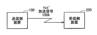
図1は、本発明の第1の実施の形態に係る受信側装置200を含むテレビ放送信号100Aの受送信システムの構成例を示すブロック図である。この受送信システムは、例えば、有線(ケーブルTVなど)や無線(地上デジタル波、衛星波など)を介してテレビ放送信号を送信する送信側装置100と、上記の有線や無線を介して送信側装置100からのテレビ放送信号を受信する受信側装置200とを備えている。なお、受信側装置200が本発明の「表示装置」の一具体例に相当する。
<First Embodiment>
[Configuration of TV broadcast signal transmission / reception system]
FIG. 1 is a block diagram showing a configuration example of a system for receiving and transmitting a
テレビ放送信号100Aは、二次元表示(平面表示)用の映像データ、または三次元表示(立体表示)用の映像データを含んでいる。ここで、二次元表示用の映像データとは、視点情報を持たない二次元映像データを指している。また、三次元表示用の映像データとは、視点情報を持った二次元映像データを指しており、三次元表示用の映像データは、視点が互いに異なる複数の二次元映像データを含んで構成されている。送信側装置100は、例えば、放送局に設置されたテレビ放送信号送信装置、またはインターネット上のサーバなどである。
The
[受信側装置200の機能ブロック]
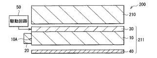
図2は、受信側装置200の構成例を示すブロック図である。受信側装置200は、二次元表示と三次元表示を行うことの可能な表示装置であり、例えば、上記の有線や無線に接続可能なテレビジョンである。受信側装置200は、例えば、アンテナ端子201、デジタルチューナ202、デマルチプレクサ203、演算回路204、およびメモリ205を有している。受信側装置200は、また、例えば、デコーダ206、映像信号処理回路207、グラフィック生成回路208、パネル駆動回路209、表示パネル210、バックライト211、音声信号処理回路212、音声増幅回路213、およびスピーカ214を有している。受信側装置200は、さらに、例えば、リモコン受信回路215、およびリモコン送信機216を有している。なお、バックライト211が本発明の「照明装置」の一具体例に相当する。
[Functional Block of Receiving Device 200]
FIG. 2 is a block diagram illustrating a configuration example of the reception-
アンテナ端子201は、受信アンテナ(図示せず)で受信されたテレビ放送信号を入力する端子である。デジタルチューナ202は、例えば、アンテナ端子201に入力されたテレビ放送信号を処理して、ユーザの選択チャネルに対応した所定のトランスポートストリームを出力するようになっている。デマルチプレクサ203は、例えば、デジタルチューナ202で得られたトランスポートストリームから、ユーザの選択チャネルに対応したパーシャルTS(Transport Stream)を抽出するようになっている。
The antenna terminal 201 is a terminal for inputting a television broadcast signal received by a receiving antenna (not shown). For example, the
演算回路204は、受信側装置200の各部の動作を制御するものである。演算回路204は、例えば、デマルチプレクサ203で得られたパーシャルTSをメモリ205内に格納したり、メモリ205から読み出したパーシャルTSをデコーダ206に送信したりするようになっている。また、演算回路204は、例えば、二次元表示または三次元表示を指定する制御信号204Aを映像信号処理回路207およびバックライト211に送信するようになっている。演算回路204は、上記の制御信号204Aを、例えば、メモリ205内に格納された設定情報、パーシャルTSに含まれる所定の情報、またはリモコン受信回路215から入力された設定情報に基づいて設定するようになっている。
The
メモリ205は、例えば、受信側装置200の設定情報の格納およびデータ管理を行うものである。メモリ205は、例えば、デマルチプレクサ203で得られたパーシャルTSや、表示方法などの設定情報を格納することが可能となっている。
The
デコーダ206は、例えば、デマルチプレクサ203で得られたパーシャルTSに含まれる映像PES(Packetized Elementary Stream)パケットに対してデコード処理を行うことにより映像データを得るようになっている。デコーダ206は、また、例えば、デマルチプレクサ203で得られたパーシャルTSに含まれる音声PESパケットに対してデコード処理を行うことにより音声データを得るようになっている。ここで、映像データとは、二次元表示用の映像データ、または三次元表示用の映像データを指している。
The
映像信号処理回路207およびグラフィック生成回路208は、例えば、デコーダ206で得られた映像データに対して、必要に応じてマルチ画像処理、グラフィックスデータの重畳処理等を行うようになっている。
For example, the video
映像信号処理回路207は、演算回路204から制御信号204Aとして三次元表示を指定する信号が入力された場合であって、かつ、デコーダ206から入力された映像データが三次元表示用の映像データであったときには、例えば、デコーダ206から入力された三次元表示用の映像データに含まれる、視点の互いに異なる複数の二次元映像データを用いて1つの二次元映像データを作成し、作成した二次元映像データを、グラフィック生成回路208に出力する映像データとして選択するようになっている。例えば、三次元表示用の映像データに、視点の互いに異なる2つの二次元映像データが含まれている場合には、映像信号処理回路207は、2つの二次元映像データを、水平方向に1つずつ交互に並べる処理を各行で行っていき、2つの二次元映像データが水平方向に交互に並んだ1つの映像データを作成するようになっている。同様に、例えば、三次元表示用の映像データに、視点の互いに異なる4つの二次元映像データが含まれている場合には、映像信号処理回路207は、4つの二次元映像データを、水平方向に1つずつ周期的に並べる処理を各行で行っていき、4つの二次元映像データが水平方向に1つずつ周期的に並んだ1つの映像データを作成するようになっている。
The video
映像信号処理回路207は、演算回路204から制御信号204Aとして二次元表示を指定する信号が入力された場合であって、かつ、デコーダ206から入力された映像データが三次元表示用の映像データであったときには、例えば、デコーダ206から入力された三次元表示用の映像データに含まれる、視点の互いに異なる複数の二次元映像データのいずれか1つの映像データを、グラフィック生成回路208に出力する映像データとして選択するようになっている。映像信号処理回路207は、演算回路204から制御信号204Aとして二次元表示を指定する信号が入力された場合であって、かつ、デコーダ206から入力された映像データが二次元表示用の映像データであったときには、例えば、デコーダ206から入力された二次元表示用の映像データを、グラフィック生成回路208に出力する映像データとして選択するようになっている。
The video
グラフィック生成回路208は、例えば、画面表示の際に使用するUI(User Interface)画面を生成するようになっている。パネル駆動回路209は、例えば、グラフィック生成回路208から出力された映像データに基づいて表示パネル210を駆動するようになっている。
For example, the
表示パネル210およびバックライト211の構成については、後に詳述する。音声信号処理回路212は、例えば、デコーダ206で得られた音声データに対してD/A変換等の処理を行うようになっている。音声増幅回路213は、例えば、音声信号処理回路212から出力された音声信号を増幅してスピーカ214に供給するようになっている。
The configuration of the
リモコン受信回路215は、例えば、リモコン送信機216から送信されたリモートコントロール信号を受信し、演算回路204に供給するようになっている。演算回路204は、例えば、リモートコントロール信号に従って受信側装置200の各部を制御するようになっている。
The remote
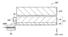
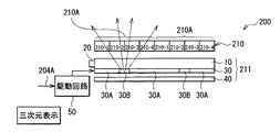
[受信側装置200の断面構成]
図3は、受信側装置200の断面構成の一例を表したものである。なお、図3は、模式的に表したものであり、実際の寸法や形状と同一であるとは限らない。受信側装置200は、表示パネル210と、表示パネル210の背後に配置されたバックライト211とを備えている。なお、バックライト211が本発明の「照明装置」の一具体例に相当する。
[Cross-sectional configuration of receiving apparatus 200]
FIG. 3 illustrates an example of a cross-sectional configuration of the reception-
表示パネル210は、映像を表示するためのものである。表示パネル210は、例えば、映像信号に応じて各画素が駆動される透過型の液晶表示パネル(LCD(Liquid Crystal Display))であり、液晶層を一対の透明基板で挟み込んだ構造となっている。具体的には、表示パネル210は、図示しないが、バックライト211側から順に、偏光板、透明基板、画素電極、配向膜、液晶層、配向膜、共通電極、カラーフィルタ、透明基板および偏光板を有している。
The
透明基板は、可視光に対して透明な基板、例えば板ガラスからなる。なお、バックライト211側の透明基板には、図示しないが、画素電極に電気的に接続されたTFT(Thin Film Transistor;薄膜トランジスタ)および配線などを含むアクティブ型の駆動回路が形成されている。画素電極および共通電極は、例えばITOからなる。画素電極は、透明基板上に格子配列されたものであり、画素ごとの電極として機能する。他方、共通電極は、カラーフィルタ上に一面に形成されたものであり、各画素電極に対して対向する共通電極として機能する。配向膜は、例えばポリイミドなどの高分子材料からなり、液晶に対して配向処理を行う。液晶層は、例えば、VA(Vertical Alignment)モード、TN(Twisted Nematic)モードまたはSTN(Super Twisted Nematic)モードの液晶からなり、駆動回路(図示せず)からの印加電圧により、バックライト211からの射出光の偏光軸の向きを画素ごとに変える機能を有する。なお、液晶の配列を多段階で変えることにより画素ごとの透過軸の向きが多段階で調整される。カラーフィルタは、液晶層を透過してきた光を、例えば、赤(R)、緑(G)および青(B)の三原色にそれぞれ色分離したり、または、R、G、Bおよび白(W)などの四色にそれぞれ色分離したりするカラーフィルタを、画素電極の配列と対応させて配列したものである。
The transparent substrate is made of a substrate transparent to visible light, for example, a plate glass. Note that an active driving circuit including a TFT (Thin Film Transistor) electrically connected to the pixel electrode and a wiring is formed on the transparent substrate on the
偏光板は、光学シャッタの一種であり、ある一定の振動方向の光(偏光)のみを通過させる。なお、偏光板は、透過軸以外の振動方向の光(偏光)を吸収する吸収型の偏光素子であってもよいが、バックライト211側に反射する反射型の偏光素子であることが輝度向上の観点から好ましい。偏光板はそれぞれ、偏光軸が互いに90度異なるように又は平行に配置されており、これによりバックライト211からの射出光が液晶層を介して透過し、あるいは遮断されるようになっている。
The polarizing plate is a kind of optical shutter, and allows only light (polarized light) in a certain vibration direction to pass therethrough. The polarizing plate may be an absorptive polarizing element that absorbs light (polarized light) in a vibration direction other than the transmission axis, but it is a reflective polarizing element that reflects to the
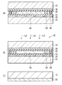
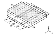
バックライト211は、二次元表示と三次元表示を行うことの可能な表示装置用の照明装置である。バックライト211は、例えば、表示パネル210を背後から照明するものであり、導光板10と、導光板10の側面に配置した光源20と、導光板11の背後に配置した光変調素子30および反射板40と、光変調素子30を駆動する駆動回路50とを備えている。
The
導光板10は、導光板10の側面に配置した光源20からの光を導光板10の上面に導くものである。この導光板10は、導光板10の上面に配置された表示パネル210に対応した形状、例えば、上面、下面および側面で囲まれた直方体状となっている。なお、以下では、導光板10の側面のうち光源20からの光が入射する側面を光入射面10Aと称するものとする。導光板10は、例えば、上面および下面の少なくとも一方の面に、所定のパターン化された形状を有しており、光入射面10Aから入射した光を散乱し、均一化する機能を有している。なお、バックライト211に印加する電圧を変調することによって輝度の均一化を行う場合には、パターン化されていない平坦な導光板を導光板10として用いることも可能である。導光板10は、例えば、ポリカーボネート樹脂(PC)やアクリル樹脂(ポリメチルメタクリレート(PMMA)などの透明熱可塑性樹脂を主に含んで構成されている。
The
光源20は、線状光源であり、例えば、熱陰極管(HCFL;Hot Cathode Fluorescent Lamp)、冷陰極管(CCFL;Cold Cathode Fluorescent Lamp)、または複数のLED(Light Emitting Diode)を一列に配置したものなどからなる。光源20が複数のLEDからなる場合には、効率、薄型化、均一性の観点から、全てのLEDがホワイトLEDであることが好ましい。なお、光源20が、例えば、赤色LED、緑色LEDおよび青色LEDを含んで構成されていてもよい。光源20は、導光板10の一の側面にだけ設けられていてもよいし(図3参照)、導光板10の2つの側面、3つの側面または全ての側面に設けられていてもよい。
The
反射板40は、導光板10の背後から光変調素子30を介して漏れ出てきた光を導光板10側に戻すものであり、例えば、反射、拡散、散乱などの機能を有している。これにより、光源20からの射出光を効率的に利用することができ、また、正面輝度の向上にも役立っている。この反射板40は、例えば、発泡PET(ポリエチレンテレフタレート)や銀蒸着フィルム、多層膜反射フィルム、白色PETなどからなる。なお、反射板40は、例えば、図4に示したように、必要に応じて省略することも可能である。
The
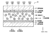
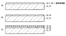
光変調素子30は、本実施の形態において、導光板10の背後(下面)に空気層を介さずに密着しており、例えば接着剤(図示せず)を介して導光板10の背後に接着されている。この光変調素子30は、例えば、図5に示したように、透明基板31、下側電極32、配向膜33、光変調層34、配向膜35、上側電極36および透明基板37を反射板40側から順に配置されたものである。なお、下側電極32が本発明の「第1電極」の一具体例に相当し、上側電極36が本発明の「第2電極」の一具体例に相当する。
In the present embodiment, the
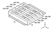
透明基板31,37は、光変調層34を支持するものであり、一般に、可視光に対して透明な基板、例えば、ガラス板や、プラスチックフィルムによって構成されている。下側電極32は、透明基板31のうち透明基板37との対向面上に設けられたものであり、例えば、図6に光変調素子30の一部を抜き出して示したように、面内全体に渡って形成された1枚のベタ膜からなる。また、上側電極36は、透明基板37のうち透明基板31との対向面上に設けられたものであり、例えば、図6に示したように、複数の部分電極36Aによって構成されている。なお、部分電極36Aが本発明の「第1部分電極」「第2部分電極」、の一具体例に相当する。
The
複数の部分電極36Aは、面内の一の方向(光入射面10Aに平行な方向)に延在する帯状の形状となっている。なお、部分電極36Bが本発明の「第1部分電極」の一具体例に相当し、部分電極36Cが本発明の「第2部分電極」の一具体例に相当する。複数の部分電極36Bは、受信側装置200において三次元表示を行うときに、線状照明光の生成に用いられるものである。複数の部分電極36Bは、受信側装置200において三次元表示を行うときの画素ピッチP2(図13参照)に対応するピッチP1(画素ピッチP2と同一ピッチまたはそれに近いピッチ)で配列されている。複数の部分電極36Bおよび複数の部分電極36Cは、配列方向(光入射面10Aと直交する方向)において交互に配列されている。なお、受信側装置200において二次元表示を行うときには、面状照明光を生成するために、全ての部分電極36Aが用いられる。
The plurality of
下側電極32および上側電極36のうち少なくとも上側電極36(バックライト211の上面側の電極)は透明な導電性材料、例えば、酸化インジウムスズ(ITO;Indium Tin Oxide)からなる。ただし、下側電極32(バックライト211の下面側の電極)については、透明な材料でなくてもよく、例えば、金属によって構成されていてもよい。なお、下側電極32が金属によって構成されている場合には、下側電極32は、反射板40と同様、導光板10の背後から光変調素子30に入射する光を反射する機能も兼ね備えていることになる。従って、この場合には、例えば、図4に示したように、反射板40をなくすることも可能である。
At least the upper electrode 36 (the electrode on the upper surface side of the backlight 211) of the
下側電極32および上側電極36を光変調素子30の法線方向から見たときに、光変調素子30のうち下側電極32および上側電極36が互いに対向している箇所に対応する部分が光変調セル30−1,30−2を構成している。光変調セル30−1は、光変調素子30のうち下側電極32および部分電極36Bが互いに対向している箇所に対応する部分であり、光変調セル30−2は、光変調素子30のうち下側電極32および部分電極36Cが互いに対向している箇所に対応する部分である。光変調セル30−1と光変調セル30−2とは互いに隣接している。
When the
各光変調セル30−1,30−2は、下側電極32および上側電極36(部分電極36A)に所定の電圧を印加することにより別個独立に駆動することの可能なものであり、下側電極32および上側電極36(部分電極36A)に印加される電圧値の大きさに応じて、光源20からの光に対して透明性を示したり、散乱性を示したりする。なお、透明性、散乱性については、光変調層34を説明する際に詳細に説明する。
Each of the light modulation cells 30-1 and 30-2 can be independently driven by applying a predetermined voltage to the
配向膜33,35は、例えば、光変調層34に用いられる液晶やモノマーを配向させるものである。配向膜の種類としては、例えば、垂直用配向膜および水平用配向膜があるが、本実施の形態では、配向膜33,35には水平用配向膜が用いられる。水平用配向膜としては、例えば、ポリイミド、ポリアミドイミド、ポリビニルアルコールなどをラビング処理することにより形成された配向膜、転写やエッチングなどにより溝形状が付与された配向膜が挙げられる。また、水平用配向膜としては、例えば、酸化ケイ素などの無機材料を斜方蒸着することにより形成された配向膜、イオンビーム照射により形成されたダイヤモンドライクカーボン配向膜、電極パターンスリットの形成された配向膜が挙げられる。透明基板31,37としてプラスチックフィルムを用いる場合には、製造工程において、透明基板31,37の表面に配向膜33,35を塗布した後の焼成温度ができるだけ低いことが好ましいことから、配向膜33,35として、100℃以下の温度で形成可能なポリアミドイミドを用いることが好ましい。
For example, the
また、垂直、水平いずれの配向膜においても、液晶とモノマーを配向させる機能があれば十分であり、通常の液晶ディスプレイに要求される電圧の繰り返し印加による信頼性などは必要ない。デバイス作成後の電圧印加による信頼性は、モノマーを重合したものと液晶との界面で決まるためである。また、配向膜を用いなくても、例えば、下側電極32および上側電極36間に電場や磁場を印加することによっても、光変調層34に用いられる液晶やモノマーを配向させることが可能である。つまり、下側電極32および上側電極36間に電場や磁場を印加しながら、紫外線照射して電圧印加状態での液晶やモノマーの配向状態を固定させることができる。配向膜の形成に電圧を用いる場合には、配向用と駆動用とで別々の電極を形成するか、液晶材料に周波数によって誘電率異方性の符号が反転する二周波液晶などを用いることができる。また、配向膜の形成に磁場を用いる場合、配向膜として磁化率異方性の大きい材料を用いることが好ましく、例えば、ベンゼン環の多い材料を用いることが好ましい。
Further, both the vertical and horizontal alignment films need only have a function of aligning the liquid crystal and the monomer, and do not require reliability due to repeated application of voltage required for a normal liquid crystal display. This is because the reliability due to the voltage application after device fabrication is determined by the interface between the polymerized monomer and the liquid crystal. Further, without using an alignment film, for example, by applying an electric field or a magnetic field between the
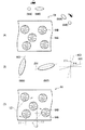
光変調層34は、電場の大きさに応じて、光源20からの光に対して散乱性もしくは透明性を示すものである。光変調層34は、例えば、図5に示したように、バルク34Aと、バルク34A内に分散された微粒子状の複数の微粒子34Bとを含んだ複合層となっている。バルク34Aおよび微粒子34Bは光学異方性を有している。なお、バルク34Aが本発明の「第2領域」に相当し、微粒子34Bが本発明の「第1領域」に相当する。
The
図7(A)は、下側電極32および上側電極36間に電圧が印加されていない時の、微粒子34B内の配向状態の一例を模式的に表したものである。なお、図7(A)において、バルク34A内の配向状態についての記載を省略した。図7(B)は、下側電極32および上側電極36間に電圧が印加されていない時の、バルク34Aおよび微粒子34Bの屈折率異方性を示す屈折率楕円体の一例を表したものである。この屈折率楕円体は、様々な方向から入射した直線偏光の屈折率をテンソル楕円体で表したものであり、光が入射する方向からの楕円体の断面を見ることによって、幾何的に屈折率を知ることができるものである。図7(C)は、下側電極32および上側電極36間に電圧が印加されていない時の、正面方向に向かう光L1と、斜め方向に向かう光L2とが光変調層34を透過する様子の一例を模式的表したものである。
FIG. 7A schematically shows an example of the orientation state in the
図8(A)は、下側電極32および上側電極36間に電圧が印加されている時の、微粒子34B内の配向状態の一例を模式的に表したものである。なお、図8(A)において、バルク34A内の配向状態についての記載を省略した。図8(B)は、下側電極32および上側電極36間に電圧が印加されている時の、バルク34Aおよび微粒子34Bの屈折率異方性を示す屈折率楕円体の一例を表したものである。図8(C)は、下側電極32および上側電極36間に電圧が印加されている時の、正面方向に向かう光L1と、斜め方向に向かう光L2とが光変調層34において散乱される様子の一例を模式的表したものである。
FIG. 8A schematically shows an example of the orientation state in the
バルク34Aおよび微粒子34Bは、例えば、図7(A),(B)に示したように、下側電極32および上側電極36間に電圧が印加されていない時に、バルク34Aの光軸AX1および微粒子34Bの光軸AX2の向きが互いに一致する(平行となる)構成となっている。なお、光軸AX1,AX2とは、偏光方向によらず屈折率が一つの値になるような光線の進行方向と平行な線を指している。また、光軸AX1および光軸AX2の向きは常に互いに一致している必要はなく、光軸AX1の向きと光軸AX2の向きとが、例えば製造誤差などによって多少ずれていてもよい。
For example, as shown in FIGS. 7A and 7B, the
また、微粒子34Bは、例えば、下側電極32および上側電極36間に電圧が印加されていない時に、光軸AX2が導光板10の光入射面10Aと平行となる構成となっている。微粒子34Bは、さらに、例えば、下側電極32および上側電極36間に電圧が印加されていない時に、光軸AX2が透明基板31,37の表面と僅かな角度θ1で交差する構成となっている(図7(B)参照)。なお、角度θ1については、微粒子34Bを構成する材料を説明する際に詳述する。
The
一方、バルク34Aは、例えば、下側電極32および上側電極36間への電圧印加の有無に拘らず、バルク34Aの光軸AX1が一定となる構成となっている。具体的には、バルク34Aは、例えば、図7(A),(B),図8(A),(B)に示したように、バルク34Aの光軸AX1が導光板10の光入射面10Aと平行となると共に透明基板31,37の表面と所定の角度θ1で交差する構成となっている。つまり、バルク34Aの光軸AX1は、下側電極32および上側電極36間に電圧が印加されていない時に、微粒子34Bの光軸AX2と平行となっている。
On the other hand, the
なお、光軸AX2が常に、導光板10の光入射面10Aと平行となると共に透明基板31,37の表面と角度θ1で交差している必要はなく、例えば製造誤差などによって透明基板31,37の表面と、角度θ1とは若干異なる角度で交差していてもよい。また、光軸AX1,AX2が常に導光板10の光入射面10Aと平行となっている必要はなく、例えば製造誤差などによって導光板10の光入射面10Aと、小さな角度で交差していてもよい。
Note that the optical axis AX2 is always parallel to the
ここで、バルク34Aおよび微粒子34Bの常光屈折率が互いに等しく、かつバルク34Aおよび微粒子34Bの異常光屈折率が互いに等しいことが好ましい。この場合に、例えば、下側電極32および上側電極36間に電圧が印加されていない時には、図7(A)に示したように、正面方向および斜め方向を含むあらゆる方向において屈折率差がほとんどなく、高い透明性が得られる。これにより、例えば、図7(C)に示したように、正面方向に向かう光L1および斜め方向に向かう光L2は、光変調層34内で散乱されることなく、光変調層34を透過する。その結果、例えば、図9(A),(B)に示したように、光源20からの光L(斜め方向からの光)は、透明領域30Aの界面(透明基板31または導光板10と空気との界面)において全反射され、透明領域30Aの輝度(黒表示の輝度)が、光変調素子30を設けていない場合(図9(B)中の一点鎖線)と比べて下がる。
Here, it is preferable that the ordinary light refractive indexes of the
また、バルク34Aおよび微粒子34Bは、例えば、下側電極32および上側電極36間に電圧が印加されている時には、図8(A)に示したように、光軸AX1および光軸AX2の向きが互いに異なる(交差する)構成となっている。また、微粒子34Bは、例えば、下側電極32および上側電極36間に電圧が印加されている時に、微粒子34Bの光軸AX2が導光板10の光入射面10Aと平行となると共に透明基板31,37の表面と角度θ1よりも大きな角度θ2(例えば90°)で交差する構成となっている。なお、角度θ2については、微粒子34Bを構成する材料を説明する際に詳述する。
Further, for example, when a voltage is applied between the
したがって、下側電極32および上側電極36間に電圧が印加されている時には、光変調層34において、正面方向および斜め方向を含むあらゆる方向において屈折率差が大きくなり、高い散乱性が得られる。これにより、例えば、図8(C)に示したように、正面方向に向かう光L1および斜め方向に向かう光L2は、光変調層34内で散乱される。その結果、例えば、図9(A)に示したように、光源20からの光L(斜め方向からの光)は、散乱領域30Bの界面(透明基板31または導光板10と空気との界面)を透過すると共に、反射板40側に透過した光は反射板40で反射され、光変調素子30を透過する。従って、散乱領域30Bの輝度は、光変調素子30を設けていない場合(図9(B)中の一点鎖線)と比べて極めて高くなり、しかも、透明領域30Aの輝度が低下した分だけ、部分的な白表示の輝度(輝度突き上げ)が大きくなる。
Therefore, when a voltage is applied between the
なお、バルク34Aおよび微粒子34Bの常光屈折率は、例えば製造誤差などによって多少ずれていてもよく、例えば、0.1以下であることが好ましく、0.05以下であることがより好ましい。また、バルク34Aおよび微粒子34Bの異常光屈折率についても、例えば製造誤差などによって多少ずれていてもよく、例えば、0.1以下であることが好ましく、0.05以下であることがより好ましい。
Note that the ordinary refractive indexes of the
また、バルク34Aの屈折率差(ΔnP=異常光屈折率neP−常光屈折率noP)や、微粒子34Bの屈折率差(ΔnL=異常光屈折率neL−常光屈折率noL)は、できるだけ大きいことが好ましく、0.05以上であることが好ましく、0.1以上であることがより好ましく、0.15以上であることがさらに好ましい。バルク34Aおよび微粒子34Bの屈折率差が大きい場合には、光変調層34の散乱能が高くなり、導光条件を容易に破壊することができ、導光板10からの光を取り出しやすいからである。
Further, the refractive index difference of the
また、バルク34Aおよび微粒子34Bは、電場に対する応答速度が互いに異なっている。バルク34Aは、例えば、電場に対して応答しない筋状構造もしくは多孔質構造となっているか、または微粒子34Bの応答速度よりも遅い応答速度を有する棒状構造となっている。バルク34Aは、例えば、低分子モノマーを重合化することにより得られた高分子材料によって形成されている。バルク34Aは、例えば、微粒子34Bの配向方向または配向膜33,35の配向方向に沿って配向した、配向性および重合性を有する材料(例えばモノマー)を熱および光の少なくとも一方によって重合させることにより形成されている。バルク34Aの筋状構造、多孔質構造もしくは棒状構造は、例えば、導光板10の光入射面10Aと平行となると共に明基板31,37の表面と僅かな角度θ1で交差する方向に長軸を有している。バルク34Aが筋状構造となっている場合に、短軸方向の平均的な筋状組織サイズは、導光光の散乱性を高くするという観点からは、0.1μm以上10μm以下となっていることが好ましく、0.2μm以上2.0μm以下の範囲であることがより好ましい。また、散乱の波長依存性を少なくするという観点からは、短軸方向の平均的な筋状組織サイズは、0.5μm以上5μm以下の範囲であることが好ましく、1〜3μmの範囲であることがより好ましい。筋状組織のサイズは、偏光顕微鏡、共焦点顕微鏡、電子顕微鏡などで観察することができる。
Further, the
一方、微粒子34Bは、例えば、液晶材料を主に含んで構成されており、バルク34Aの応答速度よりも十分に早い応答速度を有している。微粒子34B内に含まれる液晶材料(液晶分子)は、例えば棒状分子である。微粒子34B内に含まれる液晶分子として、正の屈折率異方性を有するもの(いわゆるポジ型液晶)を用いることが好ましい。
On the other hand, the
ここで、下側電極32および上側電極36間に電圧が印加されていない時には、微粒子34B内において、液晶分子の長軸方向は、光軸AX2と平行となっている。このとき、微粒子34B内の液晶分子の長軸は、導光板10の光入射面10Aと平行となると共に透明基板31,37の表面と僅かな角度θ1で交差している。つまり、微粒子34B内の液晶分子は、下側電極32および上側電極36間に電圧が印加されていない時には、導光板10の光入射面10Aと平行な面内において角度θ1だけ傾斜した状態で配向している。この角度θ1は、プレチルト角と呼ばれるもので、例えば0.1°以上30°以下の範囲であることが好ましい。この角度θ1は、0.5°以上10°以下の範囲であることがより好ましく、0.7°以上2°以下の範囲であることがさらにより好ましい。角度θ1を大きくすると、後述するような理由から散乱の効率が低下する傾向にある。また、角度θ1を小さくし過ぎると、電圧印加時に液晶の立ち上がる方位角がばらつく。例えば、180°反対側の方位(リバースチルト)に液晶が立ち上がることもある。これにより、微粒子34Bとバルク34Aとの屈折率差を有効に利用できないので、散乱効率が低くなり、輝度が小さくなる傾向にある。
Here, when no voltage is applied between the
また、下側電極32および上側電極36間に電圧が印加されている時には、微粒子34B内において、液晶分子の長軸方向は、光軸AX2と交差(もしくは直交)している。このとき、微粒子34B内の液晶分子の長軸は、導光板10の光入射面10Aと平行となると共に透明基板31,37の表面と角度θ1よりも大きな角度θ2(例えば90°)で交差している。つまり、微粒子34B内の液晶分子は、下側電極32および上側電極36間に電圧が印加されている時には、導光板10の光入射面10Aと平行な面内において角度θ2だけ傾斜した状態もしくは角度θ2(=90°)で真っ直ぐ立った状態で配向している。
Further, when a voltage is applied between the
上記した、配向性および重合性を有するモノマーとしては、光学的に異方性を有しており、かつ液晶と複合する材料であればよいが、本実施の形態では紫外線で硬化する低分子モノマーであることが好ましい。電圧無印加の状態で、液晶と、低分子モノマーを重合化することにより形成されたもの(高分子材料)との光学的異方性の方向が一致していることが好ましいので、紫外線硬化前において、液晶と低分子モノマーが同一方向に配向していることが好ましい。微粒子34Bとして液晶が用いられる場合に、その液晶が棒状分子であるときには、使用するモノマー材料の形状も棒状であることが好ましい。以上のことから、モノマー材料としては重合性と液晶性を併せ持つ材料を用いることが好ましく、例えば、重合性官能基として、アクリレート基、メタクリレート基、アクリロイルオキシ基、メタクリロイルオキシ基、ビニルエーテル基およびエポキシ基からなる群から選ばれた少なくとも1つの官能基を有することが好ましい。これらの官能基は、紫外線、赤外線または電子線を照射したり、加熱したりすることによって重合させることができる。紫外線照射時の配向度低下を抑制するために、多官能基をもつ液晶性材料を添加することもできる。バルク34Aを上述した筋状構造とする場合には、バルク34Aの原料として、2官能液晶性モノマーを用いることが好ましい。また、バルク34Aの原料に対して、液晶性を示す温度の調整を目的に単官能モノマーを添加したり、架橋密度向上を目的に3官能以上のモノマーを添加したりすることもできる。
As the above-mentioned monomer having orientation and polymerizability, any material that has optical anisotropy and is composited with liquid crystal may be used. In this embodiment, a low molecular weight monomer that cures with ultraviolet rays. It is preferable that It is preferable that the direction of optical anisotropy between the liquid crystal and the one formed by polymerizing a low molecular weight monomer (polymer material) in the state where no voltage is applied is the same before UV curing. The liquid crystal and the low molecular weight monomer are preferably aligned in the same direction. When liquid crystal is used as the
駆動回路50は、例えば、一の光変調セル30−1において微粒子34Bの光軸AX2がバルク34Aの光軸AX1と平行もしくはほぼ平行となり、他の光変調セル30Bにおいて微粒子34Bの光軸AX2がバルク34Aの光軸AX1と交差もしくは直交するように各光変調セル30Bの一対の電極(下側電極32、上側電極36)へ印加する電圧の大きさを制御するようになっている。つまり、駆動回路50は、電場制御によって、バルク34Aおよび微粒子34Bの光軸AX1,AX2の向きを互いに一致(もしくはほぼ一致)させたり、互いに異ならせたり(もしくは直交させたり)することができるようになっている。
In the
駆動回路50は、制御信号204Aとして三次元表示を指定する信号が入力されたときには、バックライト211から複数の線状照明光を出力させるようになっている。具体的には、駆動回路50は、複数の部分電極36Aのうち特定の複数の部分電極36Bに、光変調層34が散乱性を示す電圧を印加するとともに、複数の部分電極36Aのうち複数の部分電極36Bを除く複数の部分電極36Cに、光変調層34が透明性を示す電圧を印加するようになっている。言い換えると、駆動回路50は、バックライト211に含まれる全ての光変調セル30−1において微粒子34Bの光軸AX2がバルク34Aの光軸AX1と交差し、バックライト211に含まれる全ての光変調セル30−2において微粒子34Bの光軸AX2がバルク34Aの光軸AX1と平行となるように、各光変調セル30−1,30−2の一対の電極(下側電極32、部分電極36A)へ印加する電圧の大きさを制御するようになっている。
The
また、駆動回路50は、制御信号204Aとして二次元表示を指定する信号が入力されたときには、バックライト211から面状照明光を出力させるようになっている。具体的には、駆動回路50は、複数の部分電極36Aの全部に、光変調層34が散乱性を示す電圧を印加するようになっている。言い換えると、駆動回路50は、バックライト211に含まれる全ての光変調セル30−1,30−2において微粒子34Bの光軸AX2がバルク34Aの光軸AX1と交差するように、各光変調セル30−1,30−2の一対の電極(下側電極32、部分電極36A)へ印加する電圧の大きさを制御するようになっている。
Further, the
なお、駆動回路50は、制御信号204Aとして二次元表示を指定する信号が入力されるとともに、映像データに関する信号も入力されるときには、バックライト211から、映像データに対応した輝度分布を持った面状照明光(例えば、面内の一部が暗い面状照明光)を出力させるようになっていてもよい。ただし、その場合には、上部電極36が表示パネル210の画素に対応したレイアウトになっていることが好ましい。上部電極36が表示パネル210の画素に対応したレイアウトになっている場合に、駆動回路50は、映像データに応じて、複数の部分電極36Aの一部に、光変調層34が散乱性を示す電圧を印加するとともに、複数の部分電極36Aのうち、光変調層34が散乱性を示す電圧を印加していない1または複数の部分電極36Aに、光変調層34が透明性を示す電圧を印加するようになっている。
Note that the
以下に、本実施の形態のバックライト211の製造方法について、図10(A)〜(C)から図12(A)〜(C)を参照しながら説明する。
Below, the manufacturing method of the
まず、ガラス基板またはプラスチックフィルム基板からなる透明基板31,37上に、ITOなどの透明導電膜32T,36TAを形成する(図10(A))。次に、表面全体にレジスト層を形成したのち、パターニングによりレジスト層に電極パターン(下側電極32、上側電極36)を形成する(図10(B))。
First, transparent conductive films 32T and 36TA such as ITO are formed on
パターニングの方法としては、例えば、フォトリソグラフィ法、レーザー加工法、パターン印刷法、スクリーン印刷法などを用いることが可能である。また、例えば、メルク社の“ハイパーエッチ”材料を用いてスクリーン印刷した後に所定の加熱を行い、その後、水洗することでパターニングを行うこともできる。電極パターンは駆動方法および部分駆動の分割数によって決定される。電極パターンは、例えば、使用する表示装置の画素ピッチか、それに近いピッチで加工される。電極の加工幅は、加工方法にも依存するが、光りの取り出し効率という観点においてできるだけ細いことが好ましい。電極の加工幅は、例えば、50μm以下、好ましくは20μm、さらに好ましくは5μm以下である。また、ITOナノ粒子をパターン印刷した後、それを焼成することによって電極パターンを形成してもよい。 As a patterning method, for example, a photolithography method, a laser processing method, a pattern printing method, a screen printing method, or the like can be used. Further, for example, patterning can be performed by performing predetermined heating after screen printing using a “Hyper Etch” material manufactured by Merck and then washing with water. The electrode pattern is determined by the driving method and the number of divisions for partial driving. The electrode pattern is processed at, for example, a pixel pitch of a display device to be used or a pitch close thereto. The processing width of the electrode depends on the processing method, but is preferably as thin as possible from the viewpoint of light extraction efficiency. The processing width of the electrode is, for example, 50 μm or less, preferably 20 μm, and more preferably 5 μm or less. Moreover, you may form an electrode pattern by baking ITO nanoparticle after pattern printing.
次に、表面全体に配向膜33,35を塗布したのち、乾燥させ、焼成する(図10(C))。配向膜33,35としてポリイミド系材料を用いる場合には、溶媒にNMP(N−メチル−2−ピロリドン)を用いることが多いが、そのときには、大気下では200℃程度の温度が必要である。なお、この場合に、透明基板31,37としてプラスチック基板を用いる場合には、配向膜33,35を100℃で真空乾燥させ、焼成することもできる。その後、配向膜33,35に対してラビング処理を行う。これにより、配向膜33,35が水平配向用の配向膜として機能し、さらに配向膜33,35のラビング方向にプレチルトを形成することが可能となる。
Next, after the
次に、配向膜33上に、セルギャップを形成するためのスペーサ38を乾式または湿式で散布する(図11(A))。なお、真空貼り合わせ法にて光変調セル30−1,30−2を作成する場合には、滴下する混合物中にスペーサ38を混合しておいてもよい。また、スペーサ38の替わりとして、フォトリソ法によって柱スペーサを形成することもできる。
Next, a
続いて、配向膜35上に、貼り合わせおよび液晶の漏れを防止するためのシール剤39を、例えば額縁状に塗布する(図11(B))。このシール剤パターン39はディスペンサー法やスクリーン印刷法にて形成することができる。
Subsequently, a
以下に、真空貼り合わせ法(One Drop Fill法、ODF法)について説明するが、真空注入法やロール貼合方式などで光変調セル30−1を作成することも可能である。 Although the vacuum bonding method (One Drop Fill method, ODF method) is demonstrated below, it is also possible to create the light modulation cell 30-1 by a vacuum injection method, a roll bonding method, etc.
まず、セルギャップ、セル面積などから決まる体積分にあたる液晶とモノマーの混合物41を面内に均一に滴下する(図11(C))。混合物41の滴下にはリニアガイド方式の精密ディスペンサーを用いることが好ましいが、シール剤パターン39を土手として利用して、ダイコータなどを用いてもよい。
First, a liquid crystal and
液晶とモノマーは前述の材料を用いることができるが、液晶とモノマーの重量比は98:2〜50:50、好ましくは95:5〜75:25、より好ましくは92:8〜85:15である。液晶の比率を多くすることで駆動電圧を低くすることができるが、あまり液晶を多くしすぎると電圧印加時の白色度が低下したり、電圧オフ後に応答速度が低下するなど透明時に戻りにくくなったりする傾向がある。 The above-mentioned materials can be used for the liquid crystal and the monomer, but the weight ratio of the liquid crystal to the monomer is 98: 2 to 50:50, preferably 95: 5 to 75:25, more preferably 92: 8 to 85:15. is there. The drive voltage can be lowered by increasing the ratio of the liquid crystal, but if too much liquid crystal is added too much, the whiteness at the time of voltage application will decrease or the response speed will decrease after the voltage is turned off, making it difficult to return to transparency. There is a tendency to.
混合物41には、液晶とモノマーの他には、重合開始剤を添加する。使用する紫外線波長に応じて、添加する重合開始剤のモノマー比を0.1〜10重量%の範囲内で調整する。混合物41には、この他に、重合禁止剤や可塑剤、粘度調整剤なども必要に応じて添加可能である。モノマーが室温で固体やゲル状である場合には、口金やシリンジ、基板を加温することが好ましい。
A polymerization initiator is added to the
透明基板31および透明基板37を真空貼り合わせ機(図示せず)に配置したのち、真空排気し、貼り合わせを行う(図12(A))。その後、貼り合わせたものを大気に解放し、大気圧での均一加圧によってセルギャップを均一化する。セルギャップは白輝度(白色度)と駆動電圧の関係から適宜選定できるが、5〜40μm、好ましくは6〜20μm、より好ましくは7〜10μmである。
The
貼り合わせ後、必要に応じて配向処理を行うことが好ましい(図示せず)。クロスニコル偏光板の間に、貼り合わせたセルを挿入した際に、光り漏れが生じている場合には、セルをある一定時間加熱処理したり、室温で放置したりして配向させる。その後、紫外線L3を照射してモノマーを重合させてポリマー化する(図12(B))。このようにして、光変調素子30が製造される。
After bonding, it is preferable to perform an alignment treatment as necessary (not shown). If light leakage occurs when the bonded cells are inserted between the crossed Nicols polarizing plates, the cells are oriented by heat treatment for a certain period of time or by leaving them at room temperature. Then, the monomer is polymerized by irradiating with ultraviolet rays L3 to form a polymer (FIG. 12B). In this way, the
紫外線を照射している時には、セルの温度が変化しないようにすることが好ましい。赤外線カットフィルターを用いたり、光源にUV−LEDなどを用いたりすることが好ましい。紫外線照度は複合材料の組織構造に影響を与えるので、使用する液晶材料やモノマー材料、これらの組成から適宜調整することが好ましく、0.1〜500mW/cm2の範囲が好ましく、さらに好ましくは0.5〜30mW/cm2である。紫外線照度が低いほど駆動電圧が低くなる傾向にあり、生産性と特性の両面から好ましい紫外線照度を選定することができる。 It is preferable that the temperature of the cell does not change during irradiation with ultraviolet rays. It is preferable to use an infrared cut filter or a UV-LED as a light source. Since the ultraviolet illuminance affects the structure of the composite material, it is preferably adjusted as appropriate from the liquid crystal material and monomer material used, and their composition, preferably in the range of 0.1 to 500 mW / cm 2 , more preferably 0. 5 to 30 mW / cm 2 . The driving voltage tends to be lower as the ultraviolet illuminance is lower, and a preferable ultraviolet illuminance can be selected from both aspects of productivity and characteristics.
そして、導光板10に光変調素子30を貼り合わせる。貼り合わせには、粘着、接着のいずれでもよいが、導光板10の屈折率と光変調素子30の基板材料の屈折率とにできるだけ近い屈折率の材料で粘着、接着することが好ましい。最後に、下側電極32および上側電極36に引き出し線(図示せず)を取り付ける。このようにして、本実施の形態のバックライト211が製造される。
Then, the
このように、光変調素子30を作成し、最後に導光板10に光変調素子30を貼り合わせるプロセスを説明したが、導光板10の表面に、配向膜35を形成した透明基板37を予め貼り合わせてから、バックライト211を作成することもできる。また、枚葉方式、ロール・ツー・ロール方式のいずれでもバックライト211を作成することができる。
As described above, the process of creating the
次に、本実施の形態のバックライト211の作用および効果について説明する。
Next, the operation and effect of the
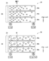
本実施の形態のバックライト211では、三次元表示のときに、各光変調セル30−1において微粒子34Bの光軸AX2がバルク34Aの光軸AX1と交差もしくは直交し、各光変調セル30−2において微粒子34Bの光軸AX2がバルク34Aの光軸AX1と平行もしくはほぼ平行となるように、各光変調セル30−1,30−2の一対の電極(下側電極32、部分電極36A)に電圧が印加される。これにより、光変調素子30において、各光変調セル30−1が散乱領域30Bとなり、各光変調セル30−2が透過領域30Aとなる。その結果、光源20から射出され、導光板10内に入射した光は、光変調素子30のうち透過領域30Aを透過し、光変調素子30のうち散乱領域30Bにおいて散乱される(図9)。この散乱光のうち散乱領域30Bの下面を透過した光は反射板40で反射され、再度、導光板10に戻されたのち、バックライト211の上面から射出される。また、散乱光のうち、散乱領域30Bの上面に向かった光は、導光板10を透過したのち、バックライト211の上面から射出される。このように、三次元表示のときには、透明領域30Aの上面からは光はほとんど射出されず、散乱領域30Bの上面から光が射出される。このようにして、例えば、図13に示したように、正面方向に、複数の線状照明光が出力される。
In the
これにより、正面方向に出力された各線状照明光が表示パネル210の背面に入射するので、例えば、各線状照明光に対応する画素配列において各画素行が三次元用画素210Aとなるように三次元表示用の二次元映像データが映像信号処理回路207で生成されたときには、各三次元用画素210内の共通の位置にある画素(例えば、図13では、210−1,210−2,210−3または210−4)には、各線状照明光が略同一の角度で入射する。その結果、各三次元用画素210A内の共通の位置にある画素からは、その画素によって変調された映像光が所定の角度で出力される。このとき、観察者は、左右の目で、互いに異なる視差の映像を観察することになるので、観察者は、表示パネル210に三次元映像(立体映像)が表示されていると認識する。
As a result, each linear illumination light output in the front direction is incident on the back surface of the
また、本実施の形態のバックライト211では、二次元表示のときに、例えば、各光変調セル30−1,30−2において微粒子34Bの光軸AX2がバルク34Aの光軸AX1と交差もしくは直交するように、各光変調セル30−1,30−2の一対の電極(下側電極32、部分電極36A)に電圧が印加される。これにより、光源20から射出され、導光板10内に入射した光は、光変調素子30の全体に形成された散乱領域30Bにおいて散乱される。この散乱光のうち散乱領域30Bの下面を透過した光は反射板40で反射され、再度、導光板10に戻されたのち、バックライト211の上面から射出される。また、散乱光のうち、散乱領域30Bの上面に向かった光は、導光板10を透過したのち、バックライト211の上面から射出される。このように、二次表示のときには、例えば、光変調素子30の上面全体から光が射出され、正面方向に、面状照明光が出力される。
In the
これにより、正面方向に出力された面状照明光が表示パネル210の背面に入射するので、例えば、各画素210Bに対応して二次元表示用の二次元映像データが映像信号処理回路207で生成されたときには、各画素210Bには、面状照明光があらゆる角度で入射し、各画素210Bからは、各画素210Bによって変調された映像光が出力される。このとき、観察者は、両目で互いに同一の映像を観察することになるので、観察者は、表示パネル210に二次元映像(平面映像)が表示されていると認識する。
As a result, the planar illumination light output in the front direction is incident on the back surface of the
ところで、本実施の形態では、三次元表示に際して、パララックスバリアを設ける必要がない。また、仮に、パララックスバリアを、バックライト211の光射出側に設けたとしても、そのときに光変調層34は線状にしか光を出力しないので、光変調層34から出力された各線状照明光がパララックスバリアで吸収される割合は極めて低い。また、本実施の形態では、三次元表示に際して、シリンドリカルレンズを必要としないので、シリンドリカルレンズに起因する収差の問題が生じる虞はない。
By the way, in this embodiment, it is not necessary to provide a parallax barrier for three-dimensional display. Even if a parallax barrier is provided on the light emission side of the
以上のことから、本実施の形態では、光変調素子30の一部を散乱領域とすることにより、複数の線状照明光がバックライト211から出力されるようにしたので、三次元表示における表示輝度および表示品質の双方を向上させることができる。
From the above, in the present embodiment, a part of the
次に、本実施の形態の受信側装置200の他の効果について説明する。
Next, another effect of reception-
一般に、PDLCは、液晶材料と等方性の低分子材料とを混合し、紫外線照射や溶媒の乾燥などにより相分離を起こさせることによって形成され、液晶材料の微小粒子が高分子材料中に分散された複合層となっている。この複合層中の液晶材料は、電圧無印加時にはランダムな方向を向いているので散乱性を示すが、電圧印加時には電場方向に配向するので、液晶材料の常光屈折率と高分子材料の屈折率とが互いに等しい場合には、正面方向(PDLCの法線方向)において高い透明性を示す。しかし、この液晶材料では、斜め方向においては、液晶材料の異常光屈折率と高分子材料の屈折率との差が顕著となり、正面方向が透明性であっても斜め方向において散乱性が発現してしまう。 In general, PDLC is formed by mixing liquid crystal material and isotropic low molecular weight material and causing phase separation by ultraviolet irradiation or solvent drying, and the fine particles of liquid crystal material are dispersed in the polymer material. It is a composite layer. The liquid crystal material in this composite layer is scattered in a random direction when no voltage is applied, but is oriented in the direction of the electric field when a voltage is applied, so the normal refractive index of the liquid crystal material and the refractive index of the polymer material Are equal to each other, high transparency is exhibited in the front direction (normal direction of PDLC). However, in this liquid crystal material, the difference between the extraordinary refractive index of the liquid crystal material and the refractive index of the polymer material becomes significant in the oblique direction, and even if the front direction is transparent, the scattering property is exhibited in the oblique direction. End up.
通常、PDLCを使った光変調素子は、表面に透明導電膜の形成された2枚のガラス板の間にPDLCを挟み込んだ構造となっていることが多い。上述したような構造を有する光変調素子に対して空気中から斜めに光が入射した場合には、その斜め方向から入射した光は空気とガラス板の屈折率差によって屈折し、より小さな角度でPDLCに入射することになる。そのため、このような光変調素子においては、大きな散乱は生じない。例えば、空気中から80°の角度で光が入射した場合には、その光のPDLCへの入射角はガラス界面での屈折によって40°程度にまで小さくなる。 Usually, a light modulation element using PDLC often has a structure in which PDLC is sandwiched between two glass plates having a transparent conductive film formed on the surface thereof. When light is incident obliquely from the air on the light modulation element having the structure as described above, the light incident from the oblique direction is refracted by the difference in refractive index between the air and the glass plate, and at a smaller angle. The light enters the PDLC. Therefore, no large scattering occurs in such a light modulation element. For example, when light is incident from the air at an angle of 80 °, the incident angle of the light on the PDLC is reduced to about 40 ° due to refraction at the glass interface.
しかし、導光板を用いたエッジライト方式では、導光板越しに光が入射するので、光が80°程度の大きな角度でPDLC中を横切ることになる。そのため、液晶材料の異常光屈折率と高分子材料の屈折率との差が大きく、さらに、より大きな角度で光がPDLC中を横切るので、散乱を受ける光路も長くなる。例えば、常光屈折率1.5、異常光屈折率1.65の液晶材料の微小粒子が屈折率1.5の高分子材料中に分散されている場合には、正面方向(PDLCの法線方向)においては屈折率差がないが、斜め方向においては屈折率差が大きくなる。このため、斜め方向の散乱性を小さくすることができないので、視野角特性が悪い。さらに、導光板上に拡散フィルムなどの光学フィルムを設けた場合には、斜め漏れ光が拡散フィルムなどによって正面方向にも拡散されるので、正面方向の光漏れが大きくなり、正面方向の変調比が低くなってしまう。 However, in the edge light system using the light guide plate, light enters through the light guide plate, so that light crosses the PDLC at a large angle of about 80 °. For this reason, the difference between the extraordinary refractive index of the liquid crystal material and the refractive index of the polymer material is large, and furthermore, since the light crosses the PDLC at a larger angle, the optical path that receives the scattering becomes longer. For example, when fine particles of a liquid crystal material having an ordinary light refractive index of 1.5 and an extraordinary light refractive index of 1.65 are dispersed in a polymer material having a refractive index of 1.5, the front direction (the normal direction of the PDLC) ), There is no difference in refractive index, but the difference in refractive index increases in the oblique direction. For this reason, since the scattering property in the oblique direction cannot be reduced, the viewing angle characteristics are poor. In addition, when an optical film such as a diffusion film is provided on the light guide plate, oblique leakage light is also diffused in the front direction by the diffusion film, etc., so that light leakage in the front direction increases, and the modulation ratio in the front direction is increased. Will be lower.
一方、本実施の形態では、バルク34Aおよび微粒子34Bが光学異方性材料を主に含んで形成されているので、斜め方向において、散乱性が小さくなり、透明性を向上させることができる。例えば、バルク34Aおよび微粒子34Bが、互いに常光屈折率が等しく、かつ互いに異常光屈折率も等しい光学異方性材料を主に含んで構成され、かつ、下側電極32および上側電極36間に電圧が印加されていない領域では、これらの光軸の向きが一致もしくはほぼ一致する。これにより、正面方向(光変調素子30の法線方向)および斜め方向を含むあらゆる方向において屈折率差が少なくなるか、またはなくなり、高い透明性が得られる。その結果、視野角の大きい範囲における光の漏洩を低減またはほとんどなくすることができ、視野角特性を良くすることができる。
On the other hand, in the present embodiment, since the
例えば、常光屈折率1.5、異常光屈折率1.65の液晶と、常光屈折率1.5、異常光屈折率1.65の液晶性モノマーとを混合し、配向膜または電界によって液晶と液晶性モノマーを配向させた状態で液晶性モノマーを重合させると、液晶の光軸と、液晶性モノマーが重合することによって形成されたポリマーの光軸とが互いに一致する。これにより、あらゆる方向で屈折率を一致させることができるので、そのようにした場合には、透明性が高い状態を実現でき、より一層、視野角特性を良くすることができる。 For example, a liquid crystal having an ordinary light refractive index of 1.5 and an extraordinary light refractive index of 1.65 is mixed with a liquid crystalline monomer having an ordinary light refractive index of 1.5 and an extraordinary light refractive index of 1.65, and the liquid crystal is formed by an alignment film or an electric field. When the liquid crystalline monomer is polymerized in a state where the liquid crystalline monomer is aligned, the optical axis of the liquid crystal and the optical axis of the polymer formed by polymerizing the liquid crystalline monomer coincide with each other. Thereby, since the refractive index can be matched in all directions, in such a case, a highly transparent state can be realized, and the viewing angle characteristics can be further improved.
また、本実施の形態では、例えば、図9(A),(B)に示したように、透明領域30Aの輝度(黒表示の輝度)が、光変調素子30を設けていない場合(図9(B)中の一点鎖線)と比べて下がっている。他方、散乱領域30Bの輝度は、光変調素子30を設けていない場合(図9(B)中の一点鎖線)と比べて極めて高くなり、しかも、透明領域30Aの輝度が低下した分だけ、部分的な白表示の輝度(輝度突き上げ)が大きくなる。
In the present embodiment, for example, as shown in FIGS. 9A and 9B, the brightness of the
ところで、輝度突き上げとは、全面白表示した場合に比べて、部分的に白表示を行った場合の輝度を高くする技術である。CRTやPDPなどでは一般によく使われている技術である。しかし、液晶ディスプレイでは、バックライトは画像にかかわらず全体に均一発光しているので、部分的に輝度を高くすることはできない。もっとも、バックライトを、複数のLEDを2次元配置したLEDバックライトとした場合には、LEDを部分的に消灯することは可能である。しかし、そのようにした場合には、LEDを消灯した暗領域からの拡散光がなくなるので、全てのLEDを点灯した場合と比べて、輝度が低くなってしまう。また、部分的に点灯しているLEDに対して流す電流を大きくすることにより、輝度を増やすことも可能であるが、そのようにした場合には、非常に短時間に大電流が流れるので、回路の負荷や信頼性の点で問題が残る。 By the way, the luminance increase is a technique for increasing the luminance when the white display is partially performed as compared with the case where the entire white display is performed. This technique is commonly used in CRT and PDP. However, in the liquid crystal display, the backlight emits light uniformly regardless of the image, and thus the brightness cannot be partially increased. However, if the backlight is an LED backlight in which a plurality of LEDs are two-dimensionally arranged, the LEDs can be partially turned off. However, in such a case, since there is no diffused light from the dark area where the LEDs are turned off, the luminance is lower than when all the LEDs are turned on. In addition, it is possible to increase the luminance by increasing the current flowing to the partially lit LED, but in such a case, a large current flows in a very short time, Problems remain in terms of circuit load and reliability.
一方、本実施の形態では、バルク34Aおよび微粒子34Bが光学異方性材料を主に含んで形成されているので、斜め方向の散乱性が抑制され、暗状態での導光板からの漏れ光が少ない。これにより、部分的な暗状態の部分から部分的な明状態の部分に導光するので、バックライト211への投入電力を増やすことなく、輝度突き上げを実現することができる。
On the other hand, in the present embodiment, since the
また、本実施の形態では、下側電極32および上側電極36間に電圧が印加されていない領域において、微粒子34Bの光軸AX2が、導光板10の光入射面10Aと平行となっており、かつ透明基板31,37の表面と僅かな角度θ1で交差している。つまり、微粒子34B内に含まれる液晶分子が、光入射面10Aと平行な面内において角度θ1だけ傾斜した状態(プレチルト角が付与された状態)で配向している。そのため、下側電極32および上側電極36間に電圧が印加された時に、微粒子34B内に含まれる液晶材料は、ランダムな方位に立ち上がることはなく、光入射面10Aと平行な面内で立ち上がる。このとき、バルク34Aおよび微粒子34Bの光軸AX1,AX2が、光入射面10Aと平行な面内において互いに交差もしくは直交する。この場合に、導光板10の光入射面10Aから入射した光において、透明基板31に対して垂直に振動する光は、微粒子34Bの異常光屈折率とバルク34Aの常光屈折率との差を感じる。このとき、微粒子34Bの異常光屈折率とバルク34Aの常光屈折率との差は大きいことから、透明基板31に対して垂直に振動する光の散乱効率が高くなる。一方、透明基板31に対して平行に振動する光は、微粒子34Bの常光屈折率とバルク34Aの異常光屈折率の差を感じる。このとき、微粒子34Bの常光屈折率とバルク34Aの異常光屈折率の差も大きいことから、透明基板31に対して平行に振動する光の散乱効率も高くなる。従って、下側電極32および上側電極36間に電圧が印加された領域を伝播する光は、斜め方向の成分を多く含む。例えば、導光板10としてアクリル導光板を用いた場合には、下側電極32および上側電極36間に電圧が印加された領域内の光は、41.8°以上の角度で伝播する。その結果、斜め方向を含むあらゆる方向において屈折率差が大きくなり、高い散乱性が得られるので、表示輝度を向上させることができる。また、上記の輝度突き上げの効果により、表示輝度をさらに向上させることができる。
In the present embodiment, the optical axis AX2 of the
ところで、例えば、電圧無印加時に導光板10の光入射面10Aに垂直に、バルク34Aおよび微粒子34Bの光軸AX1,AX2を配置し、下側電極32および上側電極36間に電圧が印加された時に、微粒子34B内に含まれる液晶材料が、光入射面10Aと垂直な面内で立ち上がるようにした場合には、透明基板31に対して垂直に振動する光は、前述した場合と同様に、微粒子34Bの異常光屈折率とバルク34Aの常光屈折率との差を感じるが、透明基板31に対して平行方向に振動する光は、微粒子34Bの常光屈折率とバルク34Aの常光屈折率との差を感じることになる。ここで、微粒子34Bの常光屈折率とバルク34Aの常光屈折率との差は、ほとんどないか、または全くない。そのため、光入射面10Aから入射した光において、透明基板31に対して垂直に振動する光は、前述した場合と同様に大きな屈折率差を感じるが、透明基板31に対して平行方向に振動する光は、屈折率差をほとんど感じないか、または全く感じない。その結果、透明基板31に対して垂直に振動する光の散乱効率は高くなるが、透明基板31に対して平行に振動する光の散乱効率は低いか、または、ゼロとなる。従って、光入射面10Aに対して光軸AX1,AX2を垂直に配置した場合には、光入射面10Aに対して光軸AX1,AX2を平行に配置した場合に比べて、散乱効率が低くなるので、導光板10から取り出せる輝度が、本実施の形態の光変調素子30よりも低くなる。
By the way, for example, when no voltage is applied, the optical axes AX1 and AX2 of the
以上のことから、本実施の形態では、視野角の大きい範囲における光の漏洩を低減またはほとんどなくしつつ、表示輝度を向上させることができる。その結果、正面方向の変調比を高くすることができる。 From the above, in this embodiment, display luminance can be improved while reducing or hardly eliminating light leakage in a range with a large viewing angle. As a result, the modulation ratio in the front direction can be increased.
<第2の実施の形態>
次に、本発明の第2の実施の形態に係るバックライトについて説明する。本実施の形態のバックライトでは、配向膜33,35として垂直用配向膜が用いられており、さらに上記実施の形態の光変調層34に代わって光変調層64が設けられている点で、上記実施の形態のバックライト211の構成と相違する。そこで、以下では、上記実施の形態の構成との共通点についての説明を適宜、省略し、上記実施の形態の構成との相違点について主に説明する。
<Second Embodiment>
Next, a backlight according to the second embodiment of the present invention will be described. In the backlight of the present embodiment, a vertical alignment film is used as the
上述したように、本実施の形態では、配向膜33,35として垂直用配向膜が用いられている。この垂直用配向膜によって、後述のバルク64Aおよび微粒子64Bが透明基板31から傾斜配向したプレチルトが形成されている。垂直用配向膜としては、シランカップリング材料や、ポリビニルアルコール(PVA)、ポリイミド系材料、界面活性剤などを用いることが可能である。例えば、これらの材料を塗布、乾燥した後にラビング処理を行うことにより、ラビング方向にプレチルトが形成される。また、透明基板31,37としてプラスチックフィルムを用いる場合には、製造工程において、透明基板31,37の表面に配向膜33,35を塗布した後の焼成温度ができるだけ低いことが好ましいことから、配向膜33,35としてアルコール系溶媒を使用することの可能なシランカップリング材料を用いることが好ましい。なお、配向膜33,35にラビング処理を施さずに、プレチルトを形成するようにしてもよい。それを実現する方法としては、例えば、配向膜33,35にセルを作成し、そのセルに対して磁場やスリット電極による斜め電場を印加しながら紫外線を照射する方法がある。
As described above, in the present embodiment, vertical alignment films are used as the
ただし、配向膜33,35として垂直用配向膜を用いるに際しては、微粒子34B内に含まれる液晶分子として、負の屈折率異方性を有するもの(いわゆるネガ型液晶)を用いることが好ましい。
However, when a vertical alignment film is used as the
次に、本実施の形態の光変調層64について説明する。光変調層64は、上記実施の形態と同様、バルク64Aと、バルク64A内に分散された微粒子状の複数の微粒子64Bとを含んだ複合層となっている。バルク64Aおよび微粒子64Bは光学異方性を有している。
Next, the
図15(A)は、下側電極32および上側電極36間に電圧が印加されていない時の、微粒子64B内の配向状態の一例を模式的に表したものである。なお、図15(A)において、バルク64A内の配向状態についての記載を省略した。図15(B)は、下側電極32および上側電極36間に電圧が印加されていない時の、バルク64Aおよび微粒子64Bの屈折率異方性を示す屈折率楕円体の一例を表したものである。図15(C)は、下側電極32および上側電極36間に電圧が印加されていない時の、正面方向に向かう光L1と、斜め方向に向かう光L2とが光変調層64を透過する様子の一例を模式的表したものである。
FIG. 15A schematically shows an example of the orientation state in the
図16(A)は、下側電極32および上側電極36間に電圧が印加されている時の、微粒子64B内の配向状態の一例を模式的に表したものである。なお、図16(A)において、バルク64A内の配向状態についての記載を省略した。図16(B)は、下側電極32および上側電極36間に電圧が印加されている時の、バルク64Aおよび微粒子64Bの屈折率異方性を示す屈折率楕円体の一例を表したものである。図16(C)は、下側電極32および上側電極36間に電圧が印加されている時の、正面方向に向かう光L1と、斜め方向に向かう光L2とが光変調層64において散乱される様子の一例を模式的表したものである。
FIG. 16A schematically shows an example of the orientation state in the
バルク64Aおよび微粒子64Bは、例えば、図15(A),(B)に示したように、下側電極32および上側電極36間に電圧が印加されていない時に、バルク64Aの光軸AX3および微粒子64Bの光軸AX4の向きが互いに一致する(平行となる)構成となっている。なお、光軸AX3,AX4とは、偏光方向によらず屈折率が一つの値になるような光線の進行方向と平行な線を指している。また、光軸AX3および光軸AX4の向きは常に互いに一致している必要はなく、光軸AX3の向きと光軸AX4の向きとが、例えば製造誤差などによって多少ずれていてもよい。
For example, as shown in FIGS. 15A and 15B, the
また、微粒子64Bは、例えば、下側電極32および上側電極36間に電圧が印加されていない時に、光軸AX4が導光板10の光入射面10Aと平行となる構成となっている。微粒子64Bは、さらに、例えば、下側電極32および上側電極36間に電圧が印加されていない時に、光軸AX4が透明基板31,37の法線と僅かな角度θ3で交差する構成となっている(図15(B)参照)。なお、角度θ3については、微粒子64Bを構成する材料を説明する際に詳述する。
The
一方、バルク64Aは、例えば、下側電極32および上側電極36間への電圧印加の有無に拘らず、バルク64Aの光軸AX4が一定となる構成となっている。具体的には、バルク64Aは、例えば、図15(A),(B),図16(A),(B)に示したように、バルク64Aの光軸AX3が導光板10の光入射面10Aと平行となると共に透明基板31,37の法線と僅かな角度θ3で交差する構成となっている。つまり、バルク64Aの光軸AX3は、下側電極32および上側電極36間に電圧が印加されていない時に、微粒子64Bの光軸AX4と平行となっている。
On the other hand, the
なお、光軸AX4が常に、導光板10の光入射面10Aと平行となると共に透明基板31,37の法線と角度θ3で交差している必要はなく、例えば製造誤差などによって透明基板31,37の法線と、角度θ3とは若干異なる角度で交差していてもよい。また、光軸AX3,AX4が常に導光板10の光入射面10Aと平行となっている必要はなく、例えば製造誤差などによって導光板10の光入射面10Aと、小さな角度で交差していてもよい。
Note that the optical axis AX4 is always parallel to the
ここで、バルク64Aおよび微粒子64Bの常光屈折率が互いに等しく、かつバルク64Aおよび微粒子64Bの異常光屈折率が互いに等しいことが好ましい。この場合に、例えば、下側電極32および上側電極36間に電圧が印加されていない時には、図15(A)に示したように、正面方向および斜め方向を含むあらゆる方向において屈折率差がほとんどなく、高い透明性が得られる。これにより、例えば、図15(C)に示したように、正面方向に向かう光L1および斜め方向に向かう光L2は、光変調層64内で散乱されることなく、光変調層64を透過する。その結果、上記実施の形態と同様、例えば、図9(A),(B)に示したように、光源20からの光L(斜め方向からの光)は、透明領域30Aの界面(透明基板31または導光板10と空気との界面)において全反射され、透明領域30Aの輝度(黒表示の輝度)が、光変調素子30を設けていない場合(図9(B)中の一点鎖線)と比べて下がる。
Here, it is preferable that the ordinary light refractive indexes of the
また、バルク64Aおよび微粒子64Bは、例えば、下側電極32および上側電極36間に電圧が印加されている時には、図16(A)に示したように、光軸AX3および光軸AX4の向きが互いに異なる(交差する)構成となっている。また、微粒子64Bは、例えば、下側電極32および上側電極36間に電圧が印加されている時に、微粒子64Bの光軸AX4が導光板10の光入射面10Aと平行となると共に透明基板31,37の法線と角度θ3よりも大きな角度θ4で交差するか、または透明基板31,37の表面と平行となる構成となっている。なお、角度θ4については、微粒子64Bを構成する材料を説明する際に詳述する。
Further, for example, when a voltage is applied between the
したがって、下側電極32および上側電極36間に電圧が印加された領域内を伝播する光は、斜め方向の成分を多く含む。例えば、導光板10としてアクリル導光板を用いた場合には、下側電極32および上側電極36間に電圧が印加された領域内の光は、41.8°以上の角度で伝播する。その結果、下側電極32および上側電極36間に電圧が印加された領域内を伝播する光においては、屈折率差が大きくなり、高い散乱性が得られる。これにより、例えば、図16(C)に示したように、正面方向に向かう光L1および斜め方向に向かう光L2は、光変調層64内で散乱される。その結果、上記実施の形態と同様、例えば、図9(A),(B)に示したように、光源20からの光L(斜め方向からの光)は、散乱領域30Bの界面(透明基板31または導光板10と空気との界面)を透過すると共に、反射板40側に透過した光は反射板40で反射され、光変調素子30を透過する。従って、散乱領域30Bの輝度は、光変調素子30を設けていない場合(図9(B)中の一点鎖線)と比べて極めて高くなり、しかも、透明領域30Aの輝度が低下した分だけ、部分的な白表示の輝度(輝度突き上げ)が大きくなる。
Therefore, the light propagating in the region where the voltage is applied between the
なお、バルク64Aおよび微粒子64Bの常光屈折率は、例えば製造誤差などによって多少ずれていてもよく、例えば、0.1以下であることが好ましく、0.05以下であることがより好ましい。また、バルク64Aおよび微粒子64Bの異常光屈折率についても、例えば製造誤差などによって多少ずれていてもよく、例えば、0.1以下であることが好ましく、0.05以下であることがより好ましい。
Note that the ordinary refractive indexes of the
また、バルク64Aの屈折率差(ΔnP=異常光屈折率neP−常光屈折率noP)や、微粒子64Bの屈折率差(ΔnL=異常光屈折率neL−常光屈折率noL)は、できるだけ大きいことが好ましく、0.05以上であることが好ましく、0.1以上であることがより好ましく、0.15以上であることがさらに好ましい。バルク64Aおよび微粒子64Bの屈折率差が大きい場合には、光変調層64の散乱能が高くなり、導光条件を容易に破壊することができ、導光板10からの光を取り出しやすいからである。
Further, the refractive index difference of the
また、バルク64Aおよび微粒子64Bは、電場に対する応答速度が互いに異なっている。バルク64Aは、例えば、電場に対して応答しない筋状構造もしくは多孔質構造となっているか、または微粒子64Bの応答速度よりも遅い応答速度を有する棒状構造となっている。バルク64Aは、例えば、低分子モノマーを重合化することにより得られた高分子材料によって形成されている。バルク64Aは、例えば、微粒子64Bの配向方向または配向膜33,35の配向方向に沿って配向した、配向性および重合性を有する材料(例えばモノマー)を熱および光の少なくとも一方によって重合させることにより形成されている。
Further, the
一方、微粒子64Bは、例えば、液晶材料を主に含んで構成されており、バルク64Aの応答速度よりも十分に早い応答速度を有している。微粒子64B内に含まれる液晶材料(液晶分子)は、例えば棒状分子である。微粒子64B内に含まれる液晶分子として、負の屈折率異方性を有するもの(いわゆるネガ型液晶)が用いられている。
On the other hand, the
ここで、下側電極32および上側電極36間に電圧が印加されていない時には、微粒子64B内において、液晶分子の長軸方向は、光軸AX4と平行となっている。このとき、微粒子64B内の液晶分子の長軸は、導光板10の光入射面10Aと平行となると共に透明基板31,37の法線と僅かな角度θ3で交差している。つまり、微粒子64B内の液晶分子は、下側電極32および上側電極36間に電圧が印加されていない時には、導光板10の光入射面10Aと平行な面内において角度θ3だけ傾斜した状態で配向している。この角度θ3は、プレチルト角と呼ばれるもので、例えば0.1°以上30°以下の範囲であることが好ましい。この角度θ3は、0.5°以上10°以下の範囲であることがより好ましく、0.7°以上2°以下の範囲であることがさらにより好ましい。角度θ3を小さくすると、後述するような理由から散乱の効率が低下する傾向にある。また、角度θ3を大きくし過ぎると(例えば、ほぼ90°にすると)、電圧印加時に液晶の立ち下がる方位角がばらつく。例えば、180°反対側の方位(リバースチルト)に液晶が立ち下がることもある。これにより、微粒子64Bとバルク64Aとの屈折率差を有効に利用できないので、散乱効率が低くなり、輝度が小さくなる傾向にある。
Here, when no voltage is applied between the
また、下側電極32および上側電極36間に電圧が印加されている時には、微粒子64B内において、液晶分子の長軸方向は、光軸AX4と交差(もしくは直交)している。このとき、微粒子64B内の液晶分子の長軸は、導光板10の光入射面10Aと平行となると共に透明基板31,37の法線と角度θ3よりも大きな角度θ4で交差している。つまり、微粒子64B内の液晶分子は、下側電極32および上側電極36間に電圧が印加されている時には、導光板10の光入射面10Aと平行な面内において角度θ4だけ傾斜した状態もしくは角度θ4(=90°)で横に寝た状態で配向している。
Further, when a voltage is applied between the
上記した、配向性および重合性を有するモノマーとしては、光学的に異方性を有しており、かつ液晶と複合する材料であればよいが、本実施の形態では紫外線で硬化する低分子モノマーであることが好ましい。電圧無印加の状態で、液晶と、低分子モノマーを重合化することにより形成されたもの(高分子材料)との光学的異方性の方向が一致していることが好ましいので、紫外線硬化前において、液晶と低分子モノマーが同一方向に配向していることが好ましい。微粒子64Bとして液晶が用いられる場合に、その液晶が棒状分子であるときには、使用するモノマー材料の形状も棒状であることが好ましい。以上のことから、モノマー材料としては重合性と液晶性を併せ持つ材料を用いることが好ましく、例えば、重合性官能基として、アクリレート基、メタクリレート基、アクリロイルオキシ基、メタクリロイルオキシ基、ビニルエーテル基およびエポキシ基からなる群から選ばれた少なくとも1つの官能基を有することが好ましい。これらの官能基は、紫外線、赤外線または電子線を照射したり、加熱したりすることによって重合させることができる。紫外線照射時の配向度低下を抑制するために、多官能基をもつ液晶性材料を添加することもできる。バルク64Aを上述した筋状構造とする場合には、バルク64Aの原料として、2官能液晶性モノマーを用いることが好ましい。また、バルク64Aの原料に対して、液晶性を示す温度の調整を目的に単官能モノマーを添加したり、架橋密度向上を目的に3官能以上のモノマーを添加したりすることもできる。
As the above-mentioned monomer having orientation and polymerizability, any material that has optical anisotropy and is composited with liquid crystal may be used. In this embodiment, a low molecular weight monomer that cures with ultraviolet rays. It is preferable that It is preferable that the direction of optical anisotropy between the liquid crystal and the one formed by polymerizing a low molecular weight monomer (polymer material) in the state where no voltage is applied is the same before UV curing. The liquid crystal and the low molecular weight monomer are preferably aligned in the same direction. When liquid crystal is used as the
次に、本実施の形態のバックライト211の作用および効果について説明する。
Next, the operation and effect of the
本実施の形態のバックライト211では、三次元表示のときに、各光変調セル30−1において微粒子64Bの光軸AX4がバルク64Aの光軸AX3と交差もしくは直交し、各光変調セル30−2において微粒子64Bの光軸AX4がバルク64Aの光軸AX3と平行もしくはほぼ平行となるように、各光変調セル30−1,30−2の一対の電極(下側電極32、部分電極36A)に電圧が印加される。これにより、光源20から射出され、導光板10内に入射した光は、光変調素子30のうち、光軸AX3と光軸AX4とが互いに平行もしくはほぼ平行となっている透過領域30Aを透過する(図9)。一方、光源20から射出され、導光板10内に入射した光は、光変調素子30のうち、光軸AX3と光軸AX4とが互いに交差もしくは直交している散乱領域30Bにおいて散乱される(図9)。この散乱光のうち散乱領域30Bの下面を透過した光は反射板40で反射され、再度、導光板10に戻されたのち、バックライト211の上面から射出される。また、散乱光のうち、散乱領域30Bの上面に向かった光は、導光板10を透過したのち、バックライト211の上面から射出される。このように、三次元表示のときには、透明領域30Aの上面からは光はほとんど射出されず、散乱領域30Bの上面から光が射出される。このようにして、例えば、図13に示したように、正面方向に、複数の線状照明光が出力される。
In the
これにより、正面方向に出力された各線状照明光が表示パネル210の背面に入射するので、例えば、各線状照明光に対応する画素配列において各画素行が三次元用画素210Aとなるように三次元表示用の二次元映像データが映像信号処理回路207で生成されたときには、各三次元用画素210内の共通の位置にある画素(例えば、図13では、210−1,210−2,210−3または210−4)には、各線状照明光が略同一の角度で入射する。その結果、各三次元用画素210A内の共通の位置にある画素からは、その画素によって変調された映像光が所定の角度で出力される。このとき、観察者は、左右の目で、互いに異なる視差の映像を観察することになるので、観察者は、表示パネル210に三次元映像(立体映像)が表示されていると認識する。
As a result, each linear illumination light output in the front direction is incident on the back surface of the
また、本実施の形態のバックライト211では、二次元表示のときに、例えば、各光変調セル30−1,30−2において微粒子64Bの光軸AX4がバルク64Aの光軸AX3と交差もしくは直交するように、各光変調セル30−1,30−2の一対の電極(下側電極32、部分電極36A)に電圧が印加される。これにより、光源20から射出され、導光板10内に入射した光は、光変調素子30の全体に形成された散乱領域30Bにおいて散乱される。この散乱光のうち散乱領域30Bの下面を透過した光は反射板40で反射され、再度、導光板10に戻されたのち、バックライト211の上面から射出される。また、散乱光のうち、散乱領域30Bの上面に向かった光は、導光板10を透過したのち、バックライト211の上面から射出される。このように、二次表示のときには、例えば、光変調素子30の上面全体から光が射出され、正面方向に、面状照明光が出力される。
Further, in the
これにより、正面方向に出力された面状照明光が表示パネル210の背面に入射するので、例えば、各画素210Bに対応して二次元表示用の二次元映像データが映像信号処理回路207で生成されたときには、各画素210Bには、面状照明光があらゆる角度で入射し、各画素210Bからは、各画素210Bによって変調された映像光が出力される。このとき、観察者は、両目で互いに同一の映像を観察することになるので、観察者は、表示パネル210に二次元映像(平面映像)が表示されていると認識する。
As a result, the planar illumination light output in the front direction is incident on the back surface of the
ところで、本実施の形態においても、三次元表示に際して、パララックスバリアを設ける必要がない。また、仮に、パララックスバリアを、バックライト211の光射出側に設けたとしても、そのときに光変調層64は線状にしか光を出力しないので、光変調層64から出力された各線状照明光がパララックスバリアで吸収される割合は極めて低い。また、本実施の形態では、三次元表示に際して、シリンドリカルレンズを必要としないので、シリンドリカルレンズに起因する収差の問題が生じる虞はない。
By the way, also in this embodiment, it is not necessary to provide a parallax barrier for three-dimensional display. Even if a parallax barrier is provided on the light emission side of the
以上のことから、本実施の形態では、光変調素子30の一部を散乱領域とすることにより、複数の線状照明光がバックライト211から出力されるようにしたので、三次元表示における表示輝度および表示品質の双方を向上させることができる。
From the above, in the present embodiment, a part of the
ところで、本実施の形態では、バルク64Aおよび微粒子64Bが光学異方性材料を主に含んで形成されているので、斜め方向において、散乱性が小さくなり、透明性を向上させることができる。例えば、バルク64Aおよび微粒子64Bが、互いに常光屈折率が等しく、かつ互いに異常光屈折率も等しい光学異方性材料を主に含んで構成され、かつ、下側電極32および上側電極36間に電圧が印加されていない領域では、これらの光軸の向きが一致もしくはほぼ一致する。これにより、正面方向(光変調素子30の法線方向)および斜め方向を含むあらゆる方向において屈折率差が少なくなるか、またはなくなり、高い透明性が得られる。その結果、視野角の大きい範囲における光の漏洩を低減またはほとんどなくすることができ、視野角特性を良くすることができる。
By the way, in this embodiment, since the
例えば、常光屈折率1.5、異常光屈折率1.65の液晶と、常光屈折率1.5、異常光屈折率1.65の液晶性モノマーとを混合し、配向膜または電界によって液晶と液晶性モノマーを配向させた状態で液晶性モノマーを重合させると、液晶の光軸と、液晶性モノマーが重合することによって形成されたポリマーの光軸とが互いに一致する。これにより、あらゆる方向で屈折率を一致させることができるので、そのようにした場合には、透明性が高い状態を実現でき、より一層、視野角特性を良くすることができる。 For example, a liquid crystal having an ordinary light refractive index of 1.5 and an extraordinary light refractive index of 1.65 is mixed with a liquid crystalline monomer having an ordinary light refractive index of 1.5 and an extraordinary light refractive index of 1.65, and the liquid crystal is formed by an alignment film or an electric field. When the liquid crystalline monomer is polymerized in a state where the liquid crystalline monomer is aligned, the optical axis of the liquid crystal and the optical axis of the polymer formed by polymerizing the liquid crystalline monomer coincide with each other. Thereby, since the refractive index can be matched in all directions, in such a case, a highly transparent state can be realized, and the viewing angle characteristics can be further improved.
また、本実施の形態では、例えば、図9(A),(B)に示したように、透明領域30Aの輝度(黒表示の輝度)が、光変調素子30を設けていない場合(図9(B)中の一点鎖線)と比べて下がっている。他方、散乱領域30Bの輝度は、光変調素子30を設けていない場合(図9(B)中の一点鎖線)と比べて極めて高くなり、しかも、透明領域30Aの輝度が低下した分だけ、部分的な白表示の輝度(輝度突き上げ)が大きくなる。これは、バルク64Aおよび微粒子64Bが光学異方性材料を主に含んで形成されており、斜め方向の散乱性が抑制され、暗状態での導光板からの漏れ光が少ないからである。従って、部分的な暗状態の部分から部分的な明状態の部分に導光するので、バックライトへの投入電力を増やすことなく、輝度突き上げを実現することができる。
In the present embodiment, for example, as shown in FIGS. 9A and 9B, the brightness of the
また、本実施の形態では、下側電極32および上側電極36間に電圧が印加されていない領域において、微粒子64Bの光軸AX4が、導光板10の光入射面10Aと平行となっており、かつ透明基板31,37の法線と僅かな角度θ3で交差している。つまり、微粒子64B内に含まれる液晶分子が、光入射面10Aと平行な面内において角度θ3だけ傾斜した状態(プレチルト角が付与された状態)で配向している。そのため、下側電極32および上側電極36間に電圧が印加された時に、微粒子64B内に含まれる液晶材料は、ランダムな方位に倒れることはなく、光入射面10Aと平行な面内で倒れる。このとき、バルク64Aおよび微粒子64Bの光軸AX3,AX4が、光入射面10Aと平行な面内において互いに交差もしくは直交する。この場合に、導光板10の光入射面10Aから入射した光において、透明基板31に対して垂直に振動する光は、微粒子64Bの常光屈折率とバルク64Aの異常光屈折率との差を感じる。このとき、微粒子64Bの常光屈折率とバルク64Aの異常光屈折率との差は大きいことから、透明基板31に対して垂直に振動する光の散乱効率が高くなる。一方、透明基板31に対して平行に振動する光は、微粒子64Bの異常光屈折率とバルク64Aの常光屈折率の差を感じる。このとき、微粒子64Bの異常光屈折率とバルク64Aの常光屈折率の差も大きいことから、透明基板31に対して平行に振動する光の散乱効率も高くなる。従って、下側電極32および上側電極36間に電圧が印加された領域を伝播する光は、斜め方向の成分を多く含む。例えば、導光板10としてアクリル導光板を用いた場合には、下側電極32および上側電極36間に電圧が印加された領域内の光は、41.8°以上の角度で伝播する。その結果、屈折率差が大きくなり、高い散乱性が得られるので、表示輝度を向上させることができる。また、上記の輝度突き上げの効果により、表示輝度をさらに向上させることができる。
In the present embodiment, the optical axis AX4 of the
ところで、例えば、電圧無印加時に導光板10の光入射面10Aに垂直に、バルク64Aおよび微粒子64Bの光軸AX3,AX4を配置し、下側電極32および上側電極36間に電圧を印加した時に、微粒子64B内に含まれる液晶材料が、光入射面10Aと垂直な面内で倒れるようにした場合には、透明基板31に対して垂直に振動する光は、前述した場合と同様に、微粒子64Bの常光屈折率とバルク64Aの異常光屈折率との差を感じるが、透明基板31に対して平行方向に振動する光は、微粒子64Bの常光屈折率とバルク64Aの常光屈折率との差を感じることになる。ここで、微粒子64Bの常光屈折率とバルク64Aの常光屈折率との差は、ほとんどないか、または全くない。そのため、光入射面10Aから入射した光において、透明基板31に対して垂直に振動する光は、前述した場合と同様に大きな屈折率差を感じるが、透明基板31に対して平行方向に振動する光は、屈折率差をほとんど感じないか、または全く感じない。その結果、透明基板31に対して垂直に振動する光の散乱効率は高くなるが、透明基板31に対して平行に振動する光の散乱効率は低いか、または、ゼロとなる。従って、光入射面10Aに対して光軸AX3,AX4を垂直に配置した場合には、光入射面10Aに対して光軸AX3,AX4を平行に配置した場合に比べて、散乱効率が低くなるので、導光板10から取り出せる輝度が、本実施の形態の光変調素子30よりも低くなる。
By the way, for example, when the optical axes AX3 and AX4 of the
また、プレチルトを形成しない場合、または、実質的にプレチルト角がほぼ90°となっている場合には、液晶が倒れる方位はランダムになるので、屈折率差は、バルク64Aおよび微粒子64Bの光軸AX3,AX4を導光板10の光入射面10Aと平行にした場合の屈折率差と垂直にした場合の屈折率差との平均になる。従って、これらの場合においても、バルク64Aおよび微粒子64Bの光軸AX3,AX4を導光板10の光入射面10Aと平行にした場合に比べて、取り出せる輝度が低くなる。
Further, when the pretilt is not formed, or when the pretilt angle is substantially 90 °, the orientation in which the liquid crystal is tilted is random, so that the refractive index difference is the optical axis of the
以上のことから、本実施の形態では、視野角の大きい範囲における光の漏洩を低減またはほとんどなくしつつ、表示輝度を向上させることができる。その結果、正面方向の変調比を高くすることができる。 From the above, in this embodiment, display luminance can be improved while reducing or hardly eliminating light leakage in a range with a large viewing angle. As a result, the modulation ratio in the front direction can be increased.
<変形例>
[第1変形例]
上記各実施の形態では、光変調素子30は、導光板10の背後(下面)に空気層を介さずに密着して接合されていたが、例えば、図17に示したように、導光板10の上面に空気層を介さずに密着して接合されていてもよい。また、光変調素子30は、例えば、図18に示したように、導光板10の内部に設けられていてもよい。ただし、この場合でも、光変調素子30は、導光板10と空気層を介さずに密着して接合されていることが必要である。
<Modification>
[First Modification]
In each of the above embodiments, the
[第2変形例]
また、上記各実施の形態では、導光板10の上に特に何も設けられていなかったが、例えば、図19に示したように、光学シート60(例えば、拡散板、拡散シート、レンズフィルム、偏光分離シートなど)を設けてもよい。このようにした場合には、導光板10から斜め方向に射出した光の一部が正面方向に立ち上がるので、変調比を効果的に向上させることができる。
[Second Modification]
In the above embodiments, nothing is provided on the
[第3変形例]
また、上記各実施の形態において、バックライト211の光射出側に、パララックスバリア70が設けられていてもよい。パララックスバリア70は、三次元表示を行うときに、バックライト211の光出力領域を、複数の電極部分36Bとの対向領域またはそれに対応する領域に限定し、散乱領域30Bに隣接する領域(例えば、透過領域30Aの端部)から出力され得るノイズ光を遮断するものである。また、パララックスバリア70は、二次元表示を行うときに、バックライト211の光出力領域を、下側電極32と上側電極36とが互いに対向する領域との対向領域またはそれに対応する領域に拡張し、光変調素子30から出力される光を透過するものである。なお、パララックスバリア70は、本発明の「光透過領域制御部」の一具体例に相当する。
[Third Modification]
In each of the above embodiments, the
パララックスバリア70は、例えば、導光板10側から順に、偏光板71、透明基板72、透明電極73、配向膜74、液晶層75、配向膜76、透明電極77、透明基板78および偏光板71Bを有している。
The
透明基板72,78は、可視光に対して透明な基板、例えば板ガラスからなる。なお、導光板10側の透明基板には、例えば、図示しないが、透明電極73に電気的に接続されたTFTおよび配線などを含むアクティブ型の駆動回路が形成されている。透明電極73,77は、例えばITOからなる。透明電極73は、例えば、図21に示したように、複数の部分電極73Aによって構成されている。複数の部分電極73Aは、透明基板72上に形成されている。
The transparent substrates 72 and 78 are made of a substrate transparent to visible light, for example, a plate glass. Note that, on the transparent substrate on the
複数の部分電極73Aは、面内の一の方向(光入射面10Aに平行な方向)に延在する帯状の形状となっている。複数の部分電極73Aのうち特定の複数の部分電極73Bの幅W3は、複数の部分電極73Aのうち複数の部分電極73Bを除く複数の部分電極73Cの幅W4よりも狭くなっている。複数の部分電極73Bは、受信側装置200において三次元表示を行うときに、線状照明光の透過、遮断に用いられるものである。複数の部分電極73Bは、受信側装置200において三次元表示を行うときの画素ピッチP2(図13参照)に対応するピッチP3(画素ピッチP2と同一ピッチまたはそれに近いピッチ)で配列されている。複数の部分電極73Bおよび複数の部分電極73Cは、配列方向(光入射面10Aと直交する方向)において交互に配列されている。なお、受信側装置200におい二次元表示を行うときには、面状照明光を生成するために、全ての部分電極73Aが用いられる。
The plurality of
透明電極77は、透明基板78上に一面に形成されたものであり、各部分電極73Aに対して対向する共通電極として機能する。配向膜74,76は、例えばポリイミドなどの高分子材料からなり、液晶に対して配向処理を行う。液晶層75は、例えば、VAモード、TNモードまたはSTNモードの液晶からなり、駆動回路50からの印加電圧により、導光板10側からの光の偏光軸の向きを部分電極73Aとの対向部分ごとに変える機能を有する。偏光板71,79は、光学シャッタの一種であり、ある一定の振動方向の光(偏光)のみを通過させる。なお、偏光板71,79は、透過軸以外の振動方向の光(偏光)を吸収する吸収型の偏光素子であってもよいが、導光板10側に反射する反射型の偏光素子であってもよい。偏光板71,79はそれぞれ、偏光軸が互いに90度異なるように又は平行に配置されており、これにより導光板10側からの光が液晶層75を介して透過し、あるいは遮断されるようになっている。
The transparent electrode 77 is formed on one surface on the transparent substrate 78, and functions as a common electrode facing each
駆動回路50は、制御信号204Aとして三次元表示を指定する信号が入力されたときには、パララックスバリア70をスリット状の光透過部として機能させるようになっている。具体的には、駆動回路50は、複数の部分電極73Aのうち特定の複数の部分電極73Bに、パララックスバリア70が透過性を示す電圧を印加するとともに、複数の部分電極73Aのうち複数の部分電極73Bを除く複数の部分電極73Cに、パララックスバリア70が遮光性を示す電圧を印加するようになっている。
When a signal designating three-dimensional display is input as the
また、駆動回路50は、制御信号204Aとして二次元表示を指定する信号が入力されたときには、パララックスバリア70全体を光透過部として機能させるようになっている。具体的には、駆動回路50は、各部分電極73Aに、パララックスバリア70が透過性を示す電圧を印加するようになっている。
In addition, when a signal designating two-dimensional display is input as the
本変形例では、バックライト211の光射出側に、パララックスバリア70が設けられているので、光変調素子30から複数の線状照明光が出力されているときに、散乱領域30Bに隣接する領域から出力され得るノイズ光を遮断することができる。これにより、三次元表示の際に、各画素210−1,210−2,210−3または210−4(図13参照)に対して各線状照明光が入射する角度とは異なる角度で入射する光を低減することができる。その結果、鮮明な3次元映像を得ることができる。
In this modification, since the
[第4変形例]
また、上記各実施の形態およびそれら変形例では、下側電極32がベタ膜となっており、上側電極36が帯状の複数の部分電極36Aによって構成されていたが、例えば、図22に示したように、下側電極32が帯状の複数の部分電極32Aによって構成され、上側電極36がベタ膜となっていてもよい。この場合、各部分電極32Aは、各部分電極36Aと同様の構成となっている。
[Fourth Modification]
Further, in each of the above-described embodiments and their modifications, the
[第5変形例]
また、例えば、図23に示したように、下側電極32が帯状の複数の部分電極32Aによって構成され、上側電極36も帯状の複数の部分電極36Aによって構成されていてもよい。
[Fifth Modification]
Further, for example, as shown in FIG. 23, the
[第6変形例]
また、例えば、下側電極32がベタ膜となっており、上側電極36が細かな引出線がついたブロック状の部分電極(図示せず)がマトリクス状に配置されたものであってもよい。この場合に、例えば、図24に示したように、光入射面10Aに平行な特定の複数の列に含まれる各部分電極が、上記の部分電極36Bとなっており、光入射面10Aに平行な他の例に含まれる各部分電極が、上記の部分電極36Cとなっている。
[Sixth Modification]
Further, for example, the
[第7変形例]
また、上記各実施の形態およびそれら変形例では、下側電極32および上側電極36の辺部が直線状となっていたが、非直線状となっていてもよい。例えば、各部分電極36B,36Cにおいて、部分電極36Bのうち部分電極36Cと隣接する辺部が、凹凸形状となっていてもよい。同様に、各部分電極36B,36Cにおいて、部分電極36Cのうち部分電極36Bと隣接する辺部が、凹凸形状となっていてもよい。また、例えば、各部分電極32B,32Cにおいて、部分電極32Bのうち部分電極32Cと隣接する辺部が、凹凸形状となっていてもよい。同様に、各部分電極32B,32Cにおいて、部分電極32Cのうち部分電極32Bと隣接する辺部が、凹凸形状となっていてもよい。
[Seventh Modification]
Further, in each of the above-described embodiments and their modifications, the sides of the
各部分電極32B,32C,36B,36Cに形成される凹凸形状は、例えば、図25(A)〜(E)に示したように、ジグザグ形状、波形状、ランプ形状、台形状またはランダム形状となっている。なお、図25(A)〜(E)において、36B(32C)は、36Bまたは36Cを意味しており、他の符号についても同様のことを意味している。
The uneven shape formed on each
各部分電極36Bの凹凸形状は、辺部に沿って配列された複数の凸部36Dによって構成されており、各部分電極36Cの凹凸形状は、辺部に沿って配列された複数の凸部36Eによって構成されている。複数の凸部36Dおよび複数の凸部36Eは、例えば、図25(A)〜(E)に示したように、互い違いに配置されている。同様に、各部分電極32Bの凹凸形状は、辺部に沿って配列された複数の凸部32Dによって構成されており、各部分電極32Cの凹凸形状は、辺部に沿って配列された複数の凸部32Eによって構成されている。複数の凸部32Dおよび複数の凸部32Eは、例えば、図25(A)〜(E)に示したように、互い違いに配置されている。
The concavo-convex shape of each
各部分電極36Bの凹凸形状の形成されている辺部と、各部分電極36Cの凹凸形状の形成されている辺部との間の間隙(スリット部分)の幅が所定の大きさ以下となっている。同様に、各部分電極32Bの凹凸形状の形成されている辺部と、各部分電極32Cの凹凸形状の形成されている辺部との間の間隙(スリット部分)の幅も所定の大きさ以下となっている。各凸部36Dの先端36Fは、例えば、図25(A)〜(E)に示したように、互いに隣接する2つの凸部36Eの間に形成される凹部36Gの外に配置されている。同様に、各凸部32Dの先端32Fは、例えば、図25(A)〜(E)に示したように、互いに隣接する2つの凸部32Eの間に形成される凹部32Gの外に配置されている。
The width of the gap (slit portion) between the side portion where the uneven shape of each
なお、各凸部36Dの先端36Fは、例えば、図26(A)〜(E)に示したように、凹部36Gの中に配置されていてもよい。同様に、各凸部32Dの先端32Fは、例えば、図26(A)〜(E)に示したように、凹部32Gの中に配置されていてもよい。図26(A)〜(E)に示したレイアウトでは、図25(A)〜(E)に示したレイアウトと比べて、スリット部分の幅をより狭くすることが可能である。
Note that the
電極の辺部に凹凸を設けることにより、線状照明光の輝度プロファイルのエッジをぼやかすことが可能であるが、線状照明光の輝度プロファイルのエッジをあまりぼやかしたくない場合には、スリット部分の幅はできるだけ狭い方が好ましい。一方、線状照明光の輝度プロファイルのエッジを積極的にぼやかしたい場合には、スリット部分の幅は狭くなり過ぎないようにすることが好ましい。線状照明光の輝度プロファイルのエッジをぼやかした場合には、例えば、観察者(図示せず)が動いたときに表示映像が突然切り替わるのをなくすることが可能である。 It is possible to blur the edge of the brightness profile of the linear illumination light by providing unevenness on the side of the electrode, but if you do not want to blur the edge of the brightness profile of the linear illumination light too much, the slit part The width of is preferably as narrow as possible. On the other hand, when it is desired to actively blur the edge of the luminance profile of the linear illumination light, it is preferable that the width of the slit portion is not too narrow. When the edge of the luminance profile of the linear illumination light is blurred, for example, it is possible to prevent the display image from switching suddenly when an observer (not shown) moves.
なお、各部分電極36Bおよび各部分電極36Cにおいて、互いに隣接する辺部の双方に対して必ずしも凹凸形状が設けられている必要はなく、いずれか一方の辺部にだけ凹凸形状が設けられていてもよい。同様に、各部分電極32Bおよび各部分電極32Cにおいて、互いに隣接する辺部の双方に対して必ずしも凹凸形状が設けられている必要はなく、いずれか一方の辺部にだけ凹凸形状が設けられていてもよい。
In each
[第8変形例]
また、上記各実施の形態およびそれら変形例では、下側電極32および上側電極36には、その内部にパターニングが施されていなかったが、下側電極32および上側電極36の少なくとも一方の内部にパターニングが施されていてもよい。この場合に、下側電極32および上側電極36のうちパターニングされた電極のパターン密度が光源20からの距離に応じて異なっている。
[Eighth Modification]
Further, in each of the above-described embodiments and their modifications, the
部分電極36Aがパターニングされている場合には、例えば、図27(A),(B)に示したように、部分電極36Aに複数の開口H1が設けられており、開口H1の密度が、上側電極36全体に関して光源20からの距離に応じて異なっている。開口H1の形状は、例えば、図27(A),(B)に示したように円形状となっている。なお、開口H1の形状は、それ以外の形状であってもよく、例えば、楕円形状、多角形状であってもよい。図27(A)に示した例では、開口H1の径r1は、光源20からの距離に拘わらず一定(r1=a1)となっており、単位面積当たりの開口H1の数が、光源20からの距離が遠くなるにつれて少なくなっている。また、図27(B)に示した例では、単位面積当たりの開口H1の数は、光源20からの距離に拘わらず一定となっており、開口H1の径r1が、光源20からの距離が遠くなるにつれて小さくなっている。なお、図27(B)には、光源20近傍の径r1がa2となっており、光源20から最も離れたところの径r1がa3(<a2)となっている場合が例示されている。従って、図27(A),(B)のいずれの例においても、開口H1の密度(単位面積当たりの開口H1の占有率)が、光源20からの距離が遠くなるにつれて疎になっている(小さくなっている)。言い換えると、上側電極36のパターン密度(上側電極36のうち開口H1以外の部分の単位面積当たりの占有率)が、光源20からの距離が遠くなるにつれて密になっている(大きくなっている)。
When the
部分電極32Aがパターニングされている場合には、例えば、図28(A),(B)に示したように、部分電極32Aに複数の開口H2が設けられており、開口H2の密度が、下側電極32全体に関して光源20からの距離に応じて異なっている。各部分電極32Aについては、開口H2の密度が、光源20からの距離に応じて異なっていてもよいし、光源20からの距離に拘わらず一定となっていてもよい。開口H2の形状は、それ以外の形状であってもよく、例えば、楕円形状、多角形状であってもよい。図28(A)に示した例では、開口H2の径r2は、光源20からの距離に拘わらず一定(r2=a4)となっており、単位面積当たりの開口H2の数が、光源20からの距離が遠くなるにつれて少なくなっている。また、図28(B)に示した例では、単位面積当たりの開口H2の数は、光源20からの距離に拘わらず一定となっており、開口H2の径r2が、光源20からの距離が遠くなるにつれて小さくなっている。なお、図28(B)には、光源20近傍の径r2がa5となっており、光源20から最も離れたところの径r2がa6(<a5)となっている場合が例示されている。従って、図28(A),(B)のいずれの例においても、開口H2の密度(単位面積当たりの開口H2の占有率)が、光源20からの距離が遠くなるにつれて疎になっている(小さくなっている)。言い換えると、下側電極32のパターン密度(下側電極32のうち開口H2以外の部分の単位面積当たりの占有率)が、光源20からの距離が遠くなるにつれて密になっている(大きくなっている)。
When the
部分電極32A,36Aの双方がパターニングされている場合には、部分電極36Aに、例えば、図27(A)または図27(B)に示したパターニングがなされ、部分電極32Aに、例えば、図28(A)または図28(B)に示したパターニングがなされている。なお、部分電極32A,36Aの双方がパターニングされている場合には、部分電極32A,36Aの双方のパターン密度が、必ず、光源20からの距離に応じて異なっている必要はない。この場合には、部分電極32Aのパターン密度(開口H2の密度)が下側電極32全体に関して光源20からの距離に応じて異なっているか、または、部分電極36Aのパターン密度(開口H1の密度)が上側電極36全体に関して光源20からの距離に応じて異なっていればよい。
When both the
部分電極32A,36Aの双方がパターニングされている場合に、開口H1が開口H2と完全に対向する位置に設けられていてもよいが、開口H1が、開口H2の一部と対向する位置に設けられているか、または、開口H2と対向しない位置に設けられている方が好ましい。また、部分電極32A,36Aの双方がパターニングされている場合に、開口H1の径と開口H2の径とが互いに等しくなっていてもよいし、互いに異なっていてもよい。
When both the
本変形例では、下側電極32および上側電極36の少なくとも一方の内部がパターニングされている。さらに、下側電極32および上側電極36のうちパターニングされた電極のパターン密度が電極全体に関して光源20からの距離に応じて異なっている。そのため、光射出領域における透明領域および散乱領域の密度分布を所望の分布にすることができる。これにより、バックライト211の光射出領域のうち光源20側の輝度を、光変調素子30を設けていない場合よりも低く抑え、かつバックライト211の光射出領域のうち光源20とは反対側の輝度を、光変調素子30を設けていない場合よりも高くすることができる。その結果、例えば、バックライト211の光射出領域全体を暗状態とした場合だけでなく、例えば、バックライト211の光射出領域全体を明状態とした場合にも、面内輝度を均一化することができる。従って、例えば、光源20に近い領域と、光源20から遠い領域とにおいて白表示をしたときに、双方の領域の白輝度を等しくすることが可能となる。また、例えば、白表示する領域よりも光源20に近い領域と、白表示する領域よりも光源20から遠い領域とにおいて黒表示をしたときに、これらの領域の黒輝度を等しくすることが可能となる。以上のことから、本変形例では、面内輝度を均一化しつつ、変調比を高くすることができる。
In this modification, at least one of the
[第9変形例]
また、上記各実施の形態およびそれら変形例において、各部分電極36Aに対して、光源20からの距離に拘わらず同一の電圧が駆動回路50から印加されるようになっていてもよいし、光源20からの距離に応じた電圧が駆動回路50から印加されるようになっていてもよい。同様に、上記各実施の形態およびそれら変形例において、各部分電極32Aに対して、光源20からの距離に拘わらず同一の電圧が駆動回路50から印加されるようになっていてもよいし、光源20からの距離に応じた電圧が駆動回路50から印加されるようになっていてもよい。
[Ninth Modification]
In each of the above-described embodiments and their modifications, the same voltage may be applied from the
上述したように、各部分電極36Aまたは各部分電極32Aに対して光源20からの距離に応じた電圧が印加される場合には、バックライト211上面の一部分だけが白輝度となるような照明光を出力したときに、その白輝度となる部分が光源20に近いときと、光源20から遠いときとで、白輝度の大きさに差が生じる虞を低減することができる。
As described above, when a voltage corresponding to the distance from the
[第10変形例]
また、上記各実施の形態およびそれら変形例において、例えば、各部分電極36Aが、さらに複数の微小電極によって構成されていてもよい。同様に、各部分電極32Aが、さらに複数の微小電極によって構成されていてもよい。また、上記各実施の形態およびそれら変形例において、ベタ膜として構成されていた上側電極36が、複数の微小電極によって構成されていてもよい。同様に、ベタ膜として構成されていた下側電極32が、複数の微小電極によって構成されていてもよい。
[Tenth Modification]
Further, in each of the above-described embodiments and their modifications, for example, each
[第11の変形例]
また、上記各実施の形態およびそれらの変形例において、各部分電極36Aのうち互いに隣接する辺部に凹凸形状が設けられている場合に、例えば、図29に示したように、互いに隣接する2つの部分電極36Aのうち一方の部分電極36Aの凹凸形状と、他方の部分電極36Aの凹凸形状との間の間隙に、部分電極36Aの辺部の凹凸形状に倣って延在する部分電極36Hがさらに設けられていてもよい。なお、図29において、36A(32A)は、36Aまたは32Aを意味しており、他の符号についても同様のことを意味している。同様に、各部分電極32Aのうち互いに隣接する辺部に凹凸形状が設けられている場合に、例えば、図29に示したように、互いに隣接する2つの部分電極32Aのうち一方の部分電極32Aの凹凸形状と、他方の部分電極32Aの凹凸形状との間の間隙に、部分電極32Aの辺部の凹凸形状に倣って延在する部分電極32Hがさらに設けられていてもよい。これらの場合に、部分電極36A,36H,32A,32Hに電圧を印加する電源(図示せず)を設け、この電源から、部分電極36A,36H,32A,32Hに対して、以下の式を満たす電圧を印加するようにすることが好ましい。そのようにした場合には、輝度の面内変化をより緩やかにすることができ、照明光における明暗の境界部分をより一層ぼかすことができる。
V1>V2>V3
V1:電源が、互いに隣接する2つの部分電極36Aの一方に印加する電圧
V2:電源が、部分電極36Hに印加する電圧
V3:電源が、互いに隣接する2つの部分電極36Aの他方に印加する電圧
V4>V5>V6
V4:電源が、互いに隣接する2つの部分電極32Aの一方に印加する電圧
V5:電源が、部分電極32Hに印加する電圧
V6:電源が、互いに隣接する2つの部分電極32Aの他方に印加する電圧
[Eleventh Modification]
Further, in each of the above-described embodiments and the modifications thereof, when uneven shapes are provided on the side portions adjacent to each other among the
V1>V2> V3
V1: Voltage applied to one of two
V4: voltage applied by the power supply to one of the two
[第12変形例]
また、上記各実施の形態およびそれら変形例において、各部分電極36Bまたは各部分電極32Bは、例えば、さらに、複数の微小電極によって構成されていてもよい。この場合に、複数の微小電極が、全体として長方形状となるように配列されていてもよいし、例えば、図30に示したように、複数の微小電極36B−1,36B−2が、面内で斜め方向に配列されていてもよい(ステップバリア形式)。また、各部分電極36Bまたは各部分電極32Bが、面内で斜め方向に延在している場合や、上述した複数の微小電極が、面内で斜め方向に配列されている場合には、例えば、図31に示したように、パララックスバリア70内の部分電極73Bも同一の方向に(斜め方向に)延在している。
[Twelfth Modification]
Moreover, in each said embodiment and those modifications, each
[第13変形例]
また、上記各実施の形態およびそれら変形例において、表示パネル210を駆動する駆動回路(図示せず)は、表示パネル210を時分割に駆動するようにしてもよい。この場合に、駆動回路50は、表示パネル210の表示の切り換えと同期して、バックライト211の三次元表示における線状照明光の出力箇所を切り替える。駆動回路50は、例えば、図32に示したように、複数の部分電極36B(32B)のうち光源20側から数えて奇数番目の電極に対応する箇所から線状照明光を出力させたのち、図33に示したように、複数の部分電極36B(32B)のうち光源20側から数えて偶数番目の電極に対応する箇所から線状照明光を出力させる。このとき、表示パネル210を駆動する駆動回路(図示せず)は、表示パネル210の複数の画素のうち、線状照明光の入射する部分に対応する画素に対して映像信号に対応する電圧を印加する。この切り替えを高速に行うことにより、観察者は、瞬間に光っている画素数の2倍の画素を知覚するようになり、実質的な解像度をあげることができる。
[Thirteenth Modification]
In each of the above-described embodiments and their modifications, a drive circuit (not shown) that drives the
1…バックライト、2…表示装置、10…導光板、10A…光入射面、20…光源、30…光変調素子、30−1,30−2…光変調セル、30A…透過領域、30B…散乱領域、31,37,72,78…透明基板、32…下側電極、32A,32B,32C,36A,36B,36C…部分電極、32D,32E,36D,36E…凸部、32F,36F…先端、32G,36G…凹部、33,35,74,76…配向膜、34,64…光変調層、34A,64A…バルク、34B,64B…微粒子、36…上側電極、38…スペーサ、39…シール剤パターン、40…反射板、41…混合物、50…駆動回路、60…光学シート、70…パララックスバリア、71,79…偏光板、73,77…透明電極、75…液晶層、100…送信側装置、100A…テレビ放送信号、200…受信側装置、201…アンテナ端子、202…デジタルチューナ、203…デマルチプレクサ、204…演算回路、204A…制御信号、205…メモリ、206…デコーダ、207…映像信号処理回路、208…グラフィック生成回路、209…パネル駆動回路、210…表示パネル、210A…三次元用画素、210B,210−1〜210−4…画素、211…バックライト、212…音声信号処理回路、213…音声増幅回路、214…スピーカ、215…リモコン受信回路、216…リモコン送信機、AX1〜AX4…光軸、H1,H2…開口。
DESCRIPTION OF
Claims (7)
導光板と、
前記導光板の側面に配置された光源と、
前記導光板の表面または内部に配置されると共に前記導光板と接着された光変調素子と、
前記光変調素子を駆動する駆動部と
を備え、
前記光変調素子は、
離間して互いに対向配置された一対の透明基板と、
前記一対の透明基板の一方の透明基板の表面に設けられた第1電極と、
前記一対の透明基板の他方の透明基板の表面に設けられた第2電極と、
前記一対の透明基板の間隙に設けられ、かつ電場の大きさに応じて、前記光源からの光に対して散乱性もしくは透明性を示す光変調層と
を有し、
前記第1電極および前記第2電極の少なくとも一方が、複数の部分電極からなり、
前記駆動部は、三次元表示を行うときには、前記複数の部分電極のうち特定の複数の第1部分電極に、前記光変調層が散乱性を示す電圧を印加するとともに、前記複数の部分電極のうち前記複数の第1部分電極を除く複数の第2部分電極に、前記光変調層が透明性を示す電圧を印加することにより、複数の線状照明光を出力させる
照明装置。 An illumination device for a display device capable of performing two-dimensional display and three-dimensional display,
A light guide plate;
A light source disposed on a side surface of the light guide plate;
A light modulation element disposed on or in the light guide plate and bonded to the light guide plate;
A drive unit for driving the light modulation element,
The light modulation element is
A pair of transparent substrates spaced apart and opposed to each other;
A first electrode provided on the surface of one of the pair of transparent substrates;
A second electrode provided on the surface of the other transparent substrate of the pair of transparent substrates;
A light modulation layer provided in a gap between the pair of transparent substrates and exhibiting scattering or transparency with respect to light from the light source according to the magnitude of an electric field,
At least one of the first electrode and the second electrode is composed of a plurality of partial electrodes,
When performing the three-dimensional display, the driving unit applies a voltage indicating the scattering property of the light modulation layer to a plurality of first partial electrodes among the plurality of partial electrodes, and Among them, an illumination device that outputs a plurality of linear illumination lights by applying a voltage indicating transparency of the light modulation layer to a plurality of second partial electrodes excluding the plurality of first partial electrodes.
請求項1に記載の照明装置。 2. The plurality of first partial electrodes and the plurality of second partial electrodes are alternately arranged one by one or plural in the arrangement direction of the plurality of linear illumination lights. Lighting equipment.
請求項2に記載の照明装置。 The illumination according to claim 2, wherein the plurality of first partial electrodes are arranged at a pitch corresponding to a pixel pitch when three-dimensional display is performed on the display device in an arrangement direction of the plurality of linear illumination lights. apparatus.
請求項1ないし請求項3のいずれか一項に記載の照明装置。 On the light output side of the lighting device, the light output region of the lighting device is limited to a region facing the plurality of first electrode portions or a region corresponding thereto, or the first electrode and the second electrode are mutually connected. The illuminating device according to any one of claims 1 to 3, further comprising a light transmission region control unit that can be extended to a region opposite to the region facing the region or a region corresponding thereto.
請求項1ないし請求項3のいずれか一項に記載の照明装置。 2. The first partial electrode of the plurality of partial electrodes is adjacent to the second partial electrode of the plurality of partial electrodes, and has a concavo-convex shape on a side portion adjacent to the second partial electrode. The illuminating device as described in any one of Claim 3 thru | or 3.
請求項1ないし請求項5のいずれか一項に記載の照明装置。 When performing the two-dimensional display, the drive unit applies a voltage indicating that the light modulation layer has a scattering property to all of the plurality of partial electrodes, thereby outputting planar illumination light whose entire surface is bright, Alternatively, a voltage at which the light modulation layer exhibits scattering properties is applied to some of the plurality of partial electrodes, and a voltage at which the light modulation layer exhibits scattering properties is not applied among the plurality of partial electrodes. The planar illumination light in which a part of the surface is dark is output by applying a voltage indicating transparency of the light modulation layer to one or a plurality of partial electrodes. The lighting device described in 1.
前記表示パネルを照明する照明装置と
を備え、
前記照明装置は、
導光板と、
前記導光板の側面に配置された光源と、
前記導光板の表面または内部に配置されると共に前記導光板と接着された光変調素子と、
前記光変調素子を駆動する駆動部と
を有し、
前記光変調素子は、
離間して互いに対向配置された一対の透明基板と、
前記一対の透明基板の一方の透明基板の表面に設けられた第1電極と、
前記一対の透明基板の他方の透明基板の表面に設けられた第2電極と、
前記一対の透明基板の間隙に設けられ、かつ電場の大きさに応じて、前記光源からの光に対して散乱性もしくは透明性を示す光変調層と
を有し、
前記第1電極および前記第2電極の少なくとも一方が、複数の部分電極からなり、
前記駆動部は、三次元表示を行うときには、前記複数の部分電極のうち特定の複数の第1部分電極に、前記光変調層が散乱性を示す電圧を印加するとともに、前記複数の部分電極のうち前記複数の第1部分電極を除く複数の第2部分電極に、前記光変調層が透明性を示す電圧を印加することにより、複数の線状照明光を出力させる
表示装置。 A display panel having a plurality of pixels arranged in a matrix, wherein the plurality of pixels are driven based on image signals for two-dimensional display or three-dimensional display;
An illumination device for illuminating the display panel,
The lighting device includes:
A light guide plate;
A light source disposed on a side surface of the light guide plate;
A light modulation element disposed on or in the light guide plate and bonded to the light guide plate;
A drive unit for driving the light modulation element,
The light modulation element is
A pair of transparent substrates spaced apart and opposed to each other;
A first electrode provided on the surface of one of the pair of transparent substrates;
A second electrode provided on the surface of the other transparent substrate of the pair of transparent substrates;
A light modulation layer provided in a gap between the pair of transparent substrates and exhibiting scattering or transparency with respect to light from the light source according to the magnitude of an electric field,
At least one of the first electrode and the second electrode is composed of a plurality of partial electrodes,
When performing the three-dimensional display, the driving unit applies a voltage indicating the scattering property of the light modulation layer to a plurality of first partial electrodes among the plurality of partial electrodes, and A display device that outputs a plurality of linear illumination lights by applying a voltage indicating transparency of the light modulation layer to a plurality of second partial electrodes excluding the plurality of first partial electrodes.
Priority Applications (7)
| Application Number | Priority Date | Filing Date | Title |
|---|---|---|---|
| JP2010089044A JP2011222237A (en) | 2010-04-07 | 2010-04-07 | Lighting system and display device |
| KR1020117028516A KR20130008442A (en) | 2010-04-07 | 2011-03-01 | Display device and lighting device |
| US13/322,014 US20120069063A1 (en) | 2010-04-07 | 2011-03-01 | Display and illumination device |
| CN201180002301.2A CN102449383B (en) | 2010-04-07 | 2011-03-01 | Display device and lighting device |
| EP11765294A EP2426401A1 (en) | 2010-04-07 | 2011-03-01 | Display device and lighting device |
| PCT/JP2011/054645 WO2011125392A1 (en) | 2010-04-07 | 2011-03-01 | Display device and lighting device |
| TW100110164A TW201211628A (en) | 2010-04-07 | 2011-03-24 | Display and illumination device |
Applications Claiming Priority (1)
| Application Number | Priority Date | Filing Date | Title |
|---|---|---|---|
| JP2010089044A JP2011222237A (en) | 2010-04-07 | 2010-04-07 | Lighting system and display device |
Publications (2)
| Publication Number | Publication Date |
|---|---|
| JP2011222237A true JP2011222237A (en) | 2011-11-04 |
| JP2011222237A5 JP2011222237A5 (en) | 2013-05-09 |
Family
ID=44762355
Family Applications (1)
| Application Number | Title | Priority Date | Filing Date |
|---|---|---|---|
| JP2010089044A Pending JP2011222237A (en) | 2010-04-07 | 2010-04-07 | Lighting system and display device |
Country Status (7)
| Country | Link |
|---|---|
| US (1) | US20120069063A1 (en) |
| EP (1) | EP2426401A1 (en) |
| JP (1) | JP2011222237A (en) |
| KR (1) | KR20130008442A (en) |
| CN (1) | CN102449383B (en) |
| TW (1) | TW201211628A (en) |
| WO (1) | WO2011125392A1 (en) |
Cited By (5)
| Publication number | Priority date | Publication date | Assignee | Title |
|---|---|---|---|---|
| JP2014077932A (en) * | 2012-10-11 | 2014-05-01 | Sony Corp | Display unit |
| US9204136B2 (en) | 2012-08-01 | 2015-12-01 | Seiko Epson Corporation | Display device and electronic apparatus |
| KR101891045B1 (en) * | 2014-11-07 | 2018-08-22 | 쓰리엠 이노베이티브 프로퍼티즈 컴파니 | Optical device including switchable diffuser |
| JP2019101101A (en) * | 2017-11-29 | 2019-06-24 | Tianma Japan株式会社 | Beam direction control device and display |
| JP2020521185A (en) * | 2017-05-14 | 2020-07-16 | レイア、インコーポレイテッドLeia Inc. | Multiview backlight, display, and method using active emitters |
Families Citing this family (23)
| Publication number | Priority date | Publication date | Assignee | Title |
|---|---|---|---|---|
| JP5467388B2 (en) | 2010-04-06 | 2014-04-09 | ソニー株式会社 | Illumination device and display device |
| JP5699786B2 (en) * | 2011-04-28 | 2015-04-15 | ソニー株式会社 | Display device and lighting device |
| JP2012252993A (en) * | 2011-05-10 | 2012-12-20 | Sony Corp | Lighting device and display device |
| JP2015045665A (en) * | 2011-12-28 | 2015-03-12 | シャープ株式会社 | Stereoscopic display device |
| JP5532075B2 (en) * | 2012-04-18 | 2014-06-25 | 凸版印刷株式会社 | Liquid crystal display |
| KR101632526B1 (en) * | 2012-04-18 | 2016-06-21 | 도판 인사츠 가부시키가이샤 | Liquid crystal display device |
| JP6035866B2 (en) * | 2012-05-22 | 2016-11-30 | ソニー株式会社 | Illumination device and display device |
| JP6098064B2 (en) * | 2012-08-08 | 2017-03-22 | ソニー株式会社 | Display device and lighting device |
| CN102789103A (en) * | 2012-08-10 | 2012-11-21 | 京东方科技集团股份有限公司 | Liquid crystal grating and display device |
| JP2014102295A (en) * | 2012-11-16 | 2014-06-05 | Sony Corp | Display device, display method and recording medium |
| KR102193561B1 (en) | 2014-03-06 | 2020-12-23 | 삼성디스플레이 주식회사 | 3d display device |
| CN104062765B (en) * | 2014-07-11 | 2016-11-23 | 张家港康得新光电材料有限公司 | 2D Yu 3D image switching display devices and lenticular elements |
| CN105807485A (en) * | 2014-12-30 | 2016-07-27 | 上海冠显光电科技有限公司 | Liquid crystal display module, device and control method |
| CN106033157A (en) * | 2015-03-07 | 2016-10-19 | 上海冠显光电科技有限公司 | A liquid crystal display device |
| JP6602695B2 (en) * | 2016-03-01 | 2019-11-06 | 株式会社ジャパンディスプレイ | Display device |
| JP2017207581A (en) * | 2016-05-17 | 2017-11-24 | 株式会社ジャパンディスプレイ | Display device |
| JP2018180333A (en) * | 2017-04-14 | 2018-11-15 | 株式会社ジャパンディスプレイ | Display device and display module |
| CN109426026B (en) | 2017-09-05 | 2022-08-23 | 京东方科技集团股份有限公司 | Display panel, preparation method thereof and display device |
| KR102557951B1 (en) * | 2018-08-27 | 2023-07-21 | 삼성전자주식회사 | Display apparatus |
| JP7160334B2 (en) * | 2018-11-22 | 2022-10-25 | 株式会社ジャパンディスプレイ | Display device |
| US11163187B2 (en) * | 2018-12-06 | 2021-11-02 | Lg Display Co., Ltd. | Backlight unit and display apparatus using the same |
| KR102148086B1 (en) * | 2018-12-17 | 2020-08-25 | 주식회사 엠알케이 | A surface illuminant and a transparent display device having the same |
| CN112017604B (en) * | 2019-05-31 | 2022-07-08 | 京东方科技集团股份有限公司 | Driving method, driving device, display device and computer readable storage medium |
Citations (3)
| Publication number | Priority date | Publication date | Assignee | Title |
|---|---|---|---|---|
| JP2007514273A (en) * | 2003-11-07 | 2007-05-31 | コーニンクレッカ フィリップス エレクトロニクス エヌ ヴィ | Waveguides for autostereoscopic displays |
| JP4386299B1 (en) * | 2008-10-09 | 2009-12-16 | 健治 吉田 | Parallax barrier, autostereoscopic image display device |
| JP2010026356A (en) * | 2008-07-23 | 2010-02-04 | Seiko Epson Corp | Electro-optical device, display method, driving method of electro-optical device, and electronic apparatus |
Family Cites Families (7)
| Publication number | Priority date | Publication date | Assignee | Title |
|---|---|---|---|---|
| JP2003162915A (en) * | 2001-11-28 | 2003-06-06 | Alps Electric Co Ltd | Planar light emitting body and liquid crystal display device |
| KR100649039B1 (en) * | 2004-01-15 | 2006-11-27 | 샤프 가부시키가이샤 | Display element, display device, and manufacturing method of display element |
| JP4480646B2 (en) * | 2005-08-25 | 2010-06-16 | 日本電気株式会社 | Optical element, light source and display device |
| JP2007094038A (en) * | 2005-09-29 | 2007-04-12 | Toshiba Matsushita Display Technology Co Ltd | Multiple image display device |
| KR100880724B1 (en) * | 2007-03-14 | 2009-02-02 | 제일모직주식회사 | Light guide panel for liquid crystal display having light diffusion material and back light unit using thereof |
| CN201107515Y (en) * | 2007-05-14 | 2008-08-27 | 安徽华东光电技术研究所 | High luminance back light source equipment for free stereoscopic display |
| TWI354115B (en) * | 2007-10-05 | 2011-12-11 | Ind Tech Res Inst | Three-dimensional display apparatus |
-
2010
- 2010-04-07 JP JP2010089044A patent/JP2011222237A/en active Pending
-
2011
- 2011-03-01 WO PCT/JP2011/054645 patent/WO2011125392A1/en active Application Filing
- 2011-03-01 CN CN201180002301.2A patent/CN102449383B/en not_active Expired - Fee Related
- 2011-03-01 KR KR1020117028516A patent/KR20130008442A/en not_active Application Discontinuation
- 2011-03-01 EP EP11765294A patent/EP2426401A1/en not_active Withdrawn
- 2011-03-01 US US13/322,014 patent/US20120069063A1/en not_active Abandoned
- 2011-03-24 TW TW100110164A patent/TW201211628A/en unknown
Patent Citations (3)
| Publication number | Priority date | Publication date | Assignee | Title |
|---|---|---|---|---|
| JP2007514273A (en) * | 2003-11-07 | 2007-05-31 | コーニンクレッカ フィリップス エレクトロニクス エヌ ヴィ | Waveguides for autostereoscopic displays |
| JP2010026356A (en) * | 2008-07-23 | 2010-02-04 | Seiko Epson Corp | Electro-optical device, display method, driving method of electro-optical device, and electronic apparatus |
| JP4386299B1 (en) * | 2008-10-09 | 2009-12-16 | 健治 吉田 | Parallax barrier, autostereoscopic image display device |
Cited By (7)
| Publication number | Priority date | Publication date | Assignee | Title |
|---|---|---|---|---|
| US9204136B2 (en) | 2012-08-01 | 2015-12-01 | Seiko Epson Corporation | Display device and electronic apparatus |
| JP2014077932A (en) * | 2012-10-11 | 2014-05-01 | Sony Corp | Display unit |
| KR101891045B1 (en) * | 2014-11-07 | 2018-08-22 | 쓰리엠 이노베이티브 프로퍼티즈 컴파니 | Optical device including switchable diffuser |
| JP2020521185A (en) * | 2017-05-14 | 2020-07-16 | レイア、インコーポレイテッドLeia Inc. | Multiview backlight, display, and method using active emitters |
| JP7089583B2 (en) | 2017-05-14 | 2022-06-22 | レイア、インコーポレイテッド | Multi-view backlight, display, and method with active emitter |
| JP2019101101A (en) * | 2017-11-29 | 2019-06-24 | Tianma Japan株式会社 | Beam direction control device and display |
| JP7083102B2 (en) | 2017-11-29 | 2022-06-10 | Tianma Japan株式会社 | Ray direction control device and display device |
Also Published As
| Publication number | Publication date |
|---|---|
| US20120069063A1 (en) | 2012-03-22 |
| CN102449383A (en) | 2012-05-09 |
| CN102449383B (en) | 2014-08-06 |
| TW201211628A (en) | 2012-03-16 |
| WO2011125392A1 (en) | 2011-10-13 |
| KR20130008442A (en) | 2013-01-22 |
| EP2426401A1 (en) | 2012-03-07 |
Similar Documents
| Publication | Publication Date | Title |
|---|---|---|
| JP2011222237A (en) | Lighting system and display device | |
| JP5699786B2 (en) | Display device and lighting device | |
| JP5991053B2 (en) | Display device and lighting device | |
| US9513487B2 (en) | Illumination device including a light modulation layer, and a display unit including the illumination device | |
| JP6112108B2 (en) | Illumination device and display device | |
| TWI550307B (en) | A display device and a lighting device | |
| JP5948813B2 (en) | Illumination device and display device | |
| JP5906649B2 (en) | Display device | |
| US9052427B2 (en) | Display and illumination unit | |
| WO2013018560A1 (en) | Illumination device and display device | |
| JP5929083B2 (en) | Display device | |
| JP5910042B2 (en) | Illumination device and display device |
Legal Events
| Date | Code | Title | Description |
|---|---|---|---|
| A521 | Written amendment |
Free format text: JAPANESE INTERMEDIATE CODE: A523 Effective date: 20130322 |
|
| A621 | Written request for application examination |
Free format text: JAPANESE INTERMEDIATE CODE: A621 Effective date: 20130322 |
|
| A131 | Notification of reasons for refusal |
Free format text: JAPANESE INTERMEDIATE CODE: A131 Effective date: 20140205 |
|
| A521 | Written amendment |
Free format text: JAPANESE INTERMEDIATE CODE: A523 Effective date: 20140402 |
|
| A02 | Decision of refusal |
Free format text: JAPANESE INTERMEDIATE CODE: A02 Effective date: 20140513 |