JP2011192808A - Imaging module, method of manufacturing the same, and endoscopic device - Google Patents
Imaging module, method of manufacturing the same, and endoscopic device Download PDFInfo
- Publication number
- JP2011192808A JP2011192808A JP2010057869A JP2010057869A JP2011192808A JP 2011192808 A JP2011192808 A JP 2011192808A JP 2010057869 A JP2010057869 A JP 2010057869A JP 2010057869 A JP2010057869 A JP 2010057869A JP 2011192808 A JP2011192808 A JP 2011192808A
- Authority
- JP
- Japan
- Prior art keywords
- solid
- imaging module
- imaging device
- wiring board
- state imaging
- Prior art date
- Legal status (The legal status is an assumption and is not a legal conclusion. Google has not performed a legal analysis and makes no representation as to the accuracy of the status listed.)
- Abandoned
Links
- 238000003384 imaging method Methods 0.000 title claims abstract description 127
- 238000004519 manufacturing process Methods 0.000 title claims description 14
- 239000006059 cover glass Substances 0.000 claims abstract description 7
- 239000000758 substrate Substances 0.000 claims description 57
- 229920005989 resin Polymers 0.000 claims description 33
- 239000011347 resin Substances 0.000 claims description 33
- 229920001187 thermosetting polymer Polymers 0.000 claims description 10
- 238000010438 heat treatment Methods 0.000 claims description 5
- 238000000034 method Methods 0.000 claims description 5
- 238000005549 size reduction Methods 0.000 abstract description 2
- 230000003247 decreasing effect Effects 0.000 abstract 1
- 239000010410 layer Substances 0.000 description 24
- 238000003780 insertion Methods 0.000 description 13
- 230000037431 insertion Effects 0.000 description 13
- 238000007789 sealing Methods 0.000 description 10
- 239000011521 glass Substances 0.000 description 8
- 238000005452 bending Methods 0.000 description 7
- 239000000463 material Substances 0.000 description 6
- 238000010586 diagram Methods 0.000 description 4
- 230000008054 signal transmission Effects 0.000 description 4
- XLYOFNOQVPJJNP-UHFFFAOYSA-N water Substances O XLYOFNOQVPJJNP-UHFFFAOYSA-N 0.000 description 4
- 230000003287 optical effect Effects 0.000 description 3
- 239000007787 solid Substances 0.000 description 3
- 230000006866 deterioration Effects 0.000 description 2
- 238000005286 illumination Methods 0.000 description 2
- 230000002093 peripheral effect Effects 0.000 description 2
- 229920001721 polyimide Polymers 0.000 description 2
- RYGMFSIKBFXOCR-UHFFFAOYSA-N Copper Chemical compound [Cu] RYGMFSIKBFXOCR-UHFFFAOYSA-N 0.000 description 1
- 239000004642 Polyimide Substances 0.000 description 1
- XUIMIQQOPSSXEZ-UHFFFAOYSA-N Silicon Chemical compound [Si] XUIMIQQOPSSXEZ-UHFFFAOYSA-N 0.000 description 1
- 239000000470 constituent Substances 0.000 description 1
- 239000011889 copper foil Substances 0.000 description 1
- 238000003745 diagnosis Methods 0.000 description 1
- 239000003822 epoxy resin Substances 0.000 description 1
- 230000001678 irradiating effect Effects 0.000 description 1
- 238000012986 modification Methods 0.000 description 1
- 230000004048 modification Effects 0.000 description 1
- 229920000647 polyepoxide Polymers 0.000 description 1
- 239000011241 protective layer Substances 0.000 description 1
- 239000004065 semiconductor Substances 0.000 description 1
- 229910052710 silicon Inorganic materials 0.000 description 1
- 239000010703 silicon Substances 0.000 description 1
- 229920002050 silicone resin Polymers 0.000 description 1
- 238000005406 washing Methods 0.000 description 1
Images


Classifications
-
- A—HUMAN NECESSITIES
- A61—MEDICAL OR VETERINARY SCIENCE; HYGIENE
- A61B—DIAGNOSIS; SURGERY; IDENTIFICATION
- A61B1/00—Instruments for performing medical examinations of the interior of cavities or tubes of the body by visual or photographical inspection, e.g. endoscopes; Illuminating arrangements therefor
- A61B1/04—Instruments for performing medical examinations of the interior of cavities or tubes of the body by visual or photographical inspection, e.g. endoscopes; Illuminating arrangements therefor combined with photographic or television appliances
- A61B1/05—Instruments for performing medical examinations of the interior of cavities or tubes of the body by visual or photographical inspection, e.g. endoscopes; Illuminating arrangements therefor combined with photographic or television appliances characterised by the image sensor, e.g. camera, being in the distal end portion
-
- A—HUMAN NECESSITIES
- A61—MEDICAL OR VETERINARY SCIENCE; HYGIENE
- A61B—DIAGNOSIS; SURGERY; IDENTIFICATION
- A61B1/00—Instruments for performing medical examinations of the interior of cavities or tubes of the body by visual or photographical inspection, e.g. endoscopes; Illuminating arrangements therefor
- A61B1/00064—Constructional details of the endoscope body
- A61B1/0011—Manufacturing of endoscope parts
-
- A—HUMAN NECESSITIES
- A61—MEDICAL OR VETERINARY SCIENCE; HYGIENE
- A61B—DIAGNOSIS; SURGERY; IDENTIFICATION
- A61B1/00—Instruments for performing medical examinations of the interior of cavities or tubes of the body by visual or photographical inspection, e.g. endoscopes; Illuminating arrangements therefor
- A61B1/04—Instruments for performing medical examinations of the interior of cavities or tubes of the body by visual or photographical inspection, e.g. endoscopes; Illuminating arrangements therefor combined with photographic or television appliances
- A61B1/05—Instruments for performing medical examinations of the interior of cavities or tubes of the body by visual or photographical inspection, e.g. endoscopes; Illuminating arrangements therefor combined with photographic or television appliances characterised by the image sensor, e.g. camera, being in the distal end portion
- A61B1/051—Details of CCD assembly
Landscapes
- Health & Medical Sciences (AREA)
- Life Sciences & Earth Sciences (AREA)
- Surgery (AREA)
- Engineering & Computer Science (AREA)
- Biomedical Technology (AREA)
- Molecular Biology (AREA)
- Pathology (AREA)
- Radiology & Medical Imaging (AREA)
- Nuclear Medicine, Radiotherapy & Molecular Imaging (AREA)
- Biophysics (AREA)
- Physics & Mathematics (AREA)
- Heart & Thoracic Surgery (AREA)
- Medical Informatics (AREA)
- Optics & Photonics (AREA)
- Animal Behavior & Ethology (AREA)
- General Health & Medical Sciences (AREA)
- Public Health (AREA)
- Veterinary Medicine (AREA)
- Manufacturing & Machinery (AREA)
- Endoscopes (AREA)
- Solid State Image Pick-Up Elements (AREA)
- Transforming Light Signals Into Electric Signals (AREA)
- Studio Devices (AREA)
Abstract
Description
本発明は撮像モジュール及びその製造方法並びに内視鏡装置に係り、特に、フレキシブル基板に固体撮像素子チップを実装する技術に関する。 The present invention relates to an imaging module, a manufacturing method thereof, and an endoscope apparatus, and more particularly to a technique for mounting a solid-state imaging element chip on a flexible substrate.
従来より、医療分野において、内視鏡装置(電子内視鏡)を利用した診断が広く行われている。内視鏡装置は、患者(被検体)の体腔内に挿入される挿入部と、挿入部の基端に連設された操作部とを備えている。挿入部の先端部には、CCD撮像素子やCMOS撮像素子などの固体撮像素子を有する撮像モジュール(撮像装置)が内蔵されている。 2. Description of the Related Art Conventionally, diagnosis using an endoscope apparatus (electronic endoscope) has been widely performed in the medical field. The endoscope apparatus includes an insertion unit that is inserted into a body cavity of a patient (subject) and an operation unit that is connected to the proximal end of the insertion unit. An image pickup module (image pickup apparatus) having a solid-state image pickup device such as a CCD image pickup device or a CMOS image pickup device is built in the distal end portion of the insertion portion.
このような内視鏡装置では、患者への挿入性をスムーズにし、患者への負担や内視鏡を操作する術者への負担を軽減するため、撮像モジュールの小型化が求められている。 In such an endoscope apparatus, in order to make insertion into a patient smooth and reduce a burden on a patient and an operator who operates the endoscope, downsizing of an imaging module is required.
例えば、特許文献1には、固体撮像素子チップの表面上に設けた電極パッドと、フレキシブル基板の端面に形成された内部配線パターンの肉厚部からなる接続用電極とが略同一平面上に配設されるように、固体撮像素子チップ側面にフレキシブル基板の端部を接着し、固体撮像素子チップの電極パッドとフレキシブル基板の接続用電極とをワイヤを用いたワイヤボンディングにより電気的に接続した固体撮像装置が開示されている。 For example, in Patent Document 1, an electrode pad provided on the surface of a solid-state imaging device chip and a connection electrode made of a thick portion of an internal wiring pattern formed on an end surface of a flexible substrate are arranged on substantially the same plane. As shown in the figure, the end of the flexible substrate is bonded to the side surface of the solid-state image sensor chip, and the electrode pad of the solid-state image sensor chip and the connection electrode of the flexible substrate are electrically connected by wire bonding using a wire. An imaging device is disclosed.
また、特許文献2には、所要の入・出力接続端子を含む配線回路が一主面に設けられたガラス基板と、前記ガラス基板の一主面上に受光面を対向させて搭載、配置された固体撮像素子と、前記固体撮像素子の端子及びガラス基板面の一方の接続端子間を電気的に接続する接続部と、前記ガラス基板面の配線回路に介挿された能動型の回路素子と、前記ガラス基板面の他方の接続端子に電気的に接続するフレキシブル配線板とを具備した固体撮像モジュールが開示されている。 Further, in Patent Document 2, a wiring substrate including necessary input / output connection terminals is mounted and arranged with a glass substrate provided on one main surface, and a light receiving surface facing one main surface of the glass substrate. A solid-state image pickup device, a connection portion for electrically connecting one of the terminals of the solid-state image pickup device and one of the connection terminals on the glass substrate surface, and an active circuit element inserted in a wiring circuit on the glass substrate surface; A solid-state imaging module including a flexible wiring board electrically connected to the other connection terminal on the glass substrate surface is disclosed.
しかしながら、特許文献1に開示される構造では、固体撮像素子チップの電極パッドとフレキシブル基板の接続用電極とがワイヤを用いたワイヤボンディングにより電気的に接続されているため、部品点数が多くなり、接続箇所の増加によって接続信頼性の低下が懸念される。 However, in the structure disclosed in Patent Document 1, since the electrode pad of the solid-state imaging device chip and the connection electrode of the flexible substrate are electrically connected by wire bonding using a wire, the number of parts increases. There is a concern that the connection reliability may decrease due to an increase in the number of connection points.
また、特許文献2に開示される構造では、固体撮像素子とフレキシブル配線板との接続にはガラス基板が介在しているため、ガラス基板の配線の分だけ撮像モジュールの小型化及び電気ノイズに対して不利である。また、特許文献1に開示される構造と同様に、接続箇所の増加によって接続信頼性の低下の懸念もある。 Further, in the structure disclosed in Patent Document 2, since a glass substrate is interposed between the solid-state imaging device and the flexible wiring board, the size of the imaging module and electrical noise are reduced by the amount of wiring on the glass substrate. It is disadvantageous. Further, like the structure disclosed in Patent Document 1, there is a concern that connection reliability may be reduced due to an increase in the number of connection points.
本発明はこのような事情に鑑みてなされたもので、撮像モジュールの小型化を図るとともに、部品点数や接続箇所の減少によって電気接続の信頼性や電気ノイズ耐性を向上させた撮像モジュール及びその製造方法並びに内視鏡装置を提供することを目的とする。 SUMMARY OF THE INVENTION The present invention has been made in view of such circumstances, and an imaging module in which the reliability of electrical connection and the resistance to electrical noise are improved by reducing the number of components and the number of connected parts while reducing the size of the imaging module and its manufacture. It is an object to provide a method and an endoscope apparatus.
前記目的を達成するために、本発明に係る撮像モジュールは、撮像面を有する固体撮像素子チップと、前記撮像面を覆うカバーガラスと、前記固体撮像素子チップが実装される配線基板と、を備えた撮像モジュールであって、前記固体撮像素子チップと前記配線基板の端部同士が互いに重なり合うオーバーラップ構造を有し、前記固体撮像素子チップの端部に形成される第1電極部と前記配線基板の端部に形成される第2電極部とがバンプを介して電気的に接続されることを特徴とする。 In order to achieve the above object, an imaging module according to the present invention includes a solid-state imaging device chip having an imaging surface, a cover glass that covers the imaging surface, and a wiring board on which the solid-state imaging device chip is mounted. An imaging module having an overlap structure in which ends of the solid-state imaging device chip and the wiring substrate overlap each other, and a first electrode portion and the wiring substrate formed at an end of the solid-state imaging device chip The second electrode part formed at the end of the electrode is electrically connected via a bump.
本発明によれば、固体撮像素子チップと配線基板の端部同士が互いに重なり合うオーバーラップ構造を有し、固体撮像素子チップの端部に形成される第1電極部と配線基板の端部に形成される第2電極部とがバンプを介して電気的に接続される。つまり、固体撮像素子チップは配線基板の端部から外側にはみ出して延設した延設配置構造を備え、固体撮像素子チップと配線基板とは、これらの間に中間接続部材(例えばワイヤボンディングによるワイヤや接続用基板など)を介在させることなく直接的に電気接続されている。これにより、撮像モジュールの小型化を図ることができるとともに、部品点数や接続箇所の削減によって電気接続の信頼性や電気ノイズ耐性が向上する。 According to the present invention, the solid-state imaging device chip and the wiring substrate have an overlapping structure in which the ends of the wiring substrate are overlapped with each other, and are formed on the end of the solid-state imaging device chip and the end of the wiring substrate. The second electrode portion is electrically connected via the bump. In other words, the solid-state imaging device chip has an extended arrangement structure that extends outward from the end portion of the wiring board, and the solid-state imaging device chip and the wiring board are provided with an intermediate connection member (for example, a wire by wire bonding) between them. Or a connection board). Accordingly, it is possible to reduce the size of the imaging module, and to improve the reliability of electrical connection and resistance to electrical noise by reducing the number of parts and the number of connection points.
本発明において、前記固体撮像素子チップと前記配線基板の端部同士は樹脂で封止固定されることが好ましい。固体撮像素子チップと配線基板との接続強度を確保することができ、電気接続の信頼性を高めることができる。 In the present invention, it is preferable that the ends of the solid-state imaging device chip and the wiring substrate are sealed and fixed with resin. The connection strength between the solid-state imaging device chip and the wiring board can be ensured, and the reliability of electrical connection can be improved.
また本発明において、前記第1の電極は、前記撮像面と同一平面上に形成されることが好ましい。固体撮像素子チップの第1の電極が撮像面と異なる平面上に形成される場合に比べて、撮像モジュールの小型化を図ることができる。また、撮像面から電極パッドまでの配線長を短くすることができ、電気ノイズ耐性も向上する。 In the present invention, it is preferable that the first electrode is formed on the same plane as the imaging surface. As compared with the case where the first electrode of the solid-state imaging device chip is formed on a plane different from the imaging surface, the imaging module can be reduced in size. In addition, the wiring length from the imaging surface to the electrode pad can be shortened, and the electrical noise resistance is also improved.
また本発明において、前記配線基板は、可撓性を有するフレキシブル基板であることが好ましく、前記フレキシブル基板は、少なくとも、ベース層、前記ベース層上に形成される配線パターン、及び前記配線パターンが形成された前記ベース層の表面を覆うカバー層を含むことがより好ましい。 In the present invention, the wiring board is preferably a flexible flexible board, and the flexible board includes at least a base layer, a wiring pattern formed on the base layer, and the wiring pattern. More preferably, it includes a cover layer covering the surface of the base layer.
また前記目的を達成するために、本発明に係る撮像モジュールの製造方法は、撮像面を有する固体撮像素子チップと、前記撮像面を覆うカバーガラスと、前記固体撮像素子チップが実装される配線基板と、を備えた撮像モジュールの製造方法であって、前記固体撮像素子チップと前記配線基板の端部同士が互いに重なり合うようにする位置合わせする工程と、前記位置合わせが行われた後、前記固体撮像素子チップの端部に形成される第1電極部と前記配線基板の端部に形成される第2電極部とをバンプを介して電気的に接続する工程と、含むことを特徴とする。 In order to achieve the above object, a method of manufacturing an imaging module according to the present invention includes a solid-state imaging device chip having an imaging surface, a cover glass that covers the imaging surface, and a wiring board on which the solid-state imaging device chip is mounted. And a step of aligning the solid-state image sensor chip and an end of the wiring board so as to overlap each other, and after the alignment is performed, the solid state And a step of electrically connecting the first electrode portion formed at the end portion of the imaging element chip and the second electrode portion formed at the end portion of the wiring board via bumps.
本発明によれば、固体撮像素子チップと配線基板の端部同士が互いに重なり合うオーバーラップ構造を有し、固体撮像素子チップの端部に形成される第1電極部と配線基板の端部に形成される第2電極部とがバンプを介して電気的に接続される。つまり、固体撮像素子チップは配線基板の端部から外側にはみ出して延設した延設配置構造を備え、固体撮像素子チップと配線基板とは、これらの間に中間接続部材(例えばワイヤボンディングによるワイヤや接続用基板など)を介在させることなく直接的に電気接続されている。これにより、撮像モジュールの小型化を図ることができるとともに、部品点数や接続箇所の削減によって電気接続の信頼性や電気ノイズ耐性が向上する。 According to the present invention, the solid-state imaging device chip and the wiring substrate have an overlapping structure in which the ends of the wiring substrate are overlapped with each other, and are formed on the end of the solid-state imaging device chip and the end of the wiring substrate. The second electrode portion is electrically connected via the bump. In other words, the solid-state imaging device chip has an extended arrangement structure that extends outward from the end portion of the wiring board, and the solid-state imaging device chip and the wiring board are provided with an intermediate connection member (for example, a wire by wire bonding) between them. Or a connection board). Accordingly, it is possible to reduce the size of the imaging module, and to improve the reliability of electrical connection and resistance to electrical noise by reducing the number of parts and the number of connection points.
また、配線基板と固体撮像素子チップとを電気的に接続するための部品点数や接続箇所が少なく、撮像モジュールの実装・組立作業性が改善される。 In addition, the number of parts and the number of connection parts for electrically connecting the wiring board and the solid-state imaging element chip are small, and the mounting and assembly workability of the imaging module is improved.
本発明において、前記固体撮像素子チップ及び前記配線基板の少なくとも一方の端部に熱硬化性樹脂を塗布する工程と、前記第1電極部及び前記第2電極部を前記バンプを介して電気的に接続した状態で前記熱硬化性樹脂を加熱して硬化させる工程と、を含むことが好ましい。固体撮像素子チップと配線基板との接続強度を容易に確保することが可能となり、電気接続の信頼性を高めることができる。 In the present invention, a step of applying a thermosetting resin to at least one end of the solid-state imaging device chip and the wiring substrate, and electrically connecting the first electrode portion and the second electrode portion via the bumps And heating and curing the thermosetting resin in a connected state. It is possible to easily secure the connection strength between the solid-state imaging device chip and the wiring board, and the reliability of electrical connection can be improved.
本発明において、前記熱硬化性樹脂の加熱は、前記固体撮像素子チップを吸着するツールを介して間接的に行われることが好ましい。また、前記熱硬化性樹脂は、180度以下で硬化する樹脂であることが好ましい。なぜなら、固体撮像素子チップの熱劣化を効果的に防止することができるからである。 In the present invention, the heating of the thermosetting resin is preferably performed indirectly through a tool that adsorbs the solid-state imaging element chip. Moreover, it is preferable that the said thermosetting resin is resin hardened | cured at 180 degrees or less. This is because thermal deterioration of the solid-state image sensor chip can be effectively prevented.
また前記目的を達成するために、本発明に係る内視鏡装置は、本発明が適用される撮像モジュールを備えたことを特徴とする。これにより、撮像モジュールが内蔵される挿入部の小型化を図ることができ、患者や術者の負担を軽減することができる。 In order to achieve the above object, an endoscope apparatus according to the present invention includes an imaging module to which the present invention is applied. Thereby, size reduction of the insertion part in which an imaging module is incorporated can be achieved, and a burden on a patient or an operator can be reduced.
本発明によれば、固体撮像素子チップと配線基板の端部同士が互いに重なり合うオーバーラップ構造を有し、固体撮像素子チップの端部に形成される第1電極部と配線基板の端部に形成される第2電極部とがバンプを介して電気的に接続される。つまり、固体撮像素子チップは配線基板の端部から外側にはみ出して延設した延設配置構造を備え、固体撮像素子チップと配線基板とは、これらの間に中間接続部材(例えばワイヤボンディングによるワイヤや接続用基板など)を介在させることなく直接的に電気接続されている。これにより、撮像モジュールの小型化を図ることができるとともに、部品点数や接続箇所の削減によって電気接続の信頼性や電気ノイズ耐性が向上する。 According to the present invention, the solid-state imaging device chip and the wiring substrate have an overlapping structure in which the ends of the wiring substrate are overlapped with each other, and are formed on the end of the solid-state imaging device chip and the end of the wiring substrate. The second electrode portion is electrically connected via the bump. In other words, the solid-state imaging device chip has an extended arrangement structure that extends outward from the end portion of the wiring board, and the solid-state imaging device chip and the wiring board are provided with an intermediate connection member (for example, a wire by wire bonding) between them. Or a connection board). Accordingly, it is possible to reduce the size of the imaging module, and to improve the reliability of electrical connection and resistance to electrical noise by reducing the number of parts and the number of connection points.
以下、添付図面に従って本発明に係る撮像モジュール及びその製造方法の好ましい実施の形態について詳説する。 Hereinafter, preferred embodiments of an imaging module and a manufacturing method thereof according to the present invention will be described in detail with reference to the accompanying drawings.
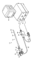
図1は、内視鏡システムを示した全体構成図である。図1に示す内視鏡システムは、主として、本発明が適用される撮像モジュールが搭載される内視鏡装置(電子内視鏡)10、プロセッサ装置26、光源装置20、及びモニタ装置50を備えて構成される。
FIG. 1 is an overall configuration diagram showing an endoscope system. The endoscope system shown in FIG. 1 mainly includes an endoscope apparatus (electronic endoscope) 10 on which an imaging module to which the present invention is applied is mounted, a processor device 26, a
内視鏡装置10は、患者(被検体)の体腔内に挿入される挿入部12と、挿入部12の基端部分に連設された手元操作部14とから主に構成される。
The
手元操作部14には、送気・送水ボタン28、吸引ボタン30、シャッターボタン32、機能切替ボタン34、及び一対のアングルノブ36、36が設けられる。また、鉗子等の処置具が挿入される鉗子口46が設けられる。
The
また、手元操作部14には、ユニバーサルケーブル16を介してLGコネクタ18が設けられており、LGコネクタ18は光源装置20に着脱自在に連結される。また、LGコネクタ18には、ケーブル22を介して電気コネクタ24が接続されており、電気コネクタ24はプロセッサ装置26に着脱自在に連結される。
The
挿入部12は、先端側(手元操作部14とは反対側)から順に、先端部44、湾曲部42、及び軟性部40から構成される。
The insertion portion 12 includes a
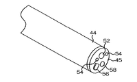
挿入部12の先端に連設された先端部44には、図2に示すように、被写体光(被観察部位からの反射光)を取り込むための観察窓52が設けられる。また、光源装置20からユニバーサルケーブル16などを通じて送られる照明光を被写体に照射するための照明窓54、54、送気・送水ボタン28を操作することによって観察窓52の汚れを落とすための洗浄水やエアーが噴射される送気・送水ノズル56、鉗子口46と連通した鉗子出口58が設けられる。
As shown in FIG. 2, an
先端部44の基端側(手元操作部14側)には、複数の湾曲駒を連結した湾曲部42が設けられている。湾曲部42は、手元操作部14のアングルノブ36、36が操作されると、挿入部12内に挿設されたワイヤが押し引きされることにより、上下左右方向に湾曲動作する。これにより、先端部44が被検体内の所望の方向に向けられる。
A bending
湾曲部42の基端側には、可撓性を有する軟性部40が設けられている。軟性部40は、先端部44が被観察部位に到達可能なように、且つ術者が手元操作部14を把持して操作する際に支障を来さない程度に患者との距離を保つために1〜数mの長さを有する。
A
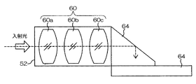
次に、先端部44の内部構造について説明する。図3は、先端部44の内部構造の要部を示した概略図である。図3に示すように、先端部44の内部には、観察窓52から取り込まれた被写体光(入射光)を集光させるための複数のレンズ60a〜60cからなる対物レンズ群60が設けられており、その後方には被写体光の光路を90度方向変換するプリズム62が設けられている。プリズム62の下端には撮像モジュール64が配置されており、プリズム62により光路が90度方向変換された被写体光は撮像モジュール64の撮像面(図3中不図示、図4に符号68として記載)に結像される。
Next, the internal structure of the
ここで、本実施形態で用いられる撮像モジュール64の構成について詳説する。図4は、先端部44に内蔵される撮像モジュール64の詳細を示した構成図であり、(a)は側面断面図、(b)は平面図である。
Here, the configuration of the
図4(a)、(b)に示すように、本実施形態の撮像モジュール64は、主として、例えばシリコーン製の半導体基板上に固体撮像素子(例えばCCD撮像素子、CMOS撮像素子など)が設けられた固体撮像素子チップ66と、固体撮像素子チップ66とプリズム62との間に配置され、固体撮像素子チップ66の撮像面(受光部)68を覆うカバーガラス70と、固体撮像素子チップ66に一端が接続されるフレキシブル基板(FPC)72とを備えて構成される。
As shown in FIGS. 4A and 4B, the
固体撮像素子チップ66の主面には、略中央部分に撮像面68が配置されており、その周辺部に撮像面68と信号の入出力を行うための複数の電極パッド74が設けられている。各電極パッド74上には、それぞれバンプ84が固着されている。
On the main surface of the solid-state
フレキシブル基板72は、絶縁性及び可撓性を有するベース層(ベース基材)76と、ベース層76の表面に形成された配線パターン78と、配線パターン78が形成されたベース層76の表面を覆うカバー層(保護層)80とから主に構成される。フレキシブル基板72は、カバー層80が固体撮像素子チップ66側(図4の下側)を向くように配置される。
The
フレキシブル基板72の構成材料の一例としては、ベース層76はポリイミドフィルム、配線パターン78は銅箔パターン、カバー層80はポリイミドカバーレイが好ましく用いられる。なお、カバー層80は、ベース層76と同様に、絶縁性及び可撓性を有する材料にて形成される。ベース層76とカバー層80とは同一材料にて形成されてもよいし、異なる材料で形成されていてもよい。
As an example of the constituent material of the
フレキシブル基板72の一端(固体撮像素子チップ66側の端部)には、固体撮像素子チップ66の電極パッド74と電気的に接続するために複数の接続端子部82が設けられている。接続端子部82は、ベース層76上で引き回された配線パターン78の端部に形成され、カバー層80で覆われずに表面に露出した部分となっている。
A plurality of
本実施形態では、固体撮像素子チップ66をフレキシブル基板72に実装するときの作業性を向上させるととともに接続端子部(リード部)82の折れ曲がり防止するために、少なくとも接続端子部82が形成される位置にはベース層76が存在するように構成される。即ち、フレキシブル基板72における固体撮像素子チップ66の実装部がフライングリード構造とならないようにされている。
In the present embodiment, at least the
固体撮像素子チップ66とフレキシブル基板72の端部同士は互いに重なり合うオーバーラップ構造となっており、固体撮像素子チップ66の電極パッド74とフレキシブル基板72の接続端子部82はバンプ84を介して電気的に接続されている。
The ends of the solid-state
また、固体撮像素子チップ66とフレキシブル基板72の端部同士の接続強度を確保するため、電極パッド74及び接続端子部82の周辺部は封止樹脂(熱硬化性樹脂)86で封止固定されている。封止樹脂86としてはACP・NCP樹脂(異方導電性ペースト・非導電性ペースト樹脂)が用いられ、例えばエポキシ系樹脂やシリコーン系樹脂が好適である。また、ACP・NCP樹脂の代わりに、ACF・NCFフィルム(異方導電性フィルム・非導電性フィルム)を用いるようにしてもよい。
Further, in order to secure the connection strength between the ends of the solid-state
図示は省略するが、フレキシブル基板72の他端にも同様な接続端子部が設けられている。この接続端子部には、プロセッサ装置26との間で信号を送受信するための信号伝送ケーブルが電気的に接続される。信号伝送ケーブルは、図1の挿入部12、手元操作部14、ユニバーサルケーブル16等に挿通されて電気コネクタ24まで延設され、プロセッサ装置26に接続される。信号伝送ケーブルは、固体撮像素子チップ66やフレキシブル基板72に実装される電子部品(不図示)などに電力を供給し、固体撮像素子チップ66で光電変換された電気信号をプロセッサ装置26に送信する。
Although illustration is omitted, a similar connection terminal portion is also provided at the other end of the
かかる構成により、先端部44の観察窓52から取り込まれた被写体光は、対物レンズ群60により集光され、プリズム62により光路が90度方向変換された後、撮像モジュール64の撮像面68に結像される。そして、撮像モジュール64で光電変換された被写体光の電気信号(撮像信号)は、フレキシブル基板72、及び信号伝送ケーブルを通じてプロセッサ装置26に出力され、プロセッサ装置26にて映像信号に変換される。これにより、プロセッサ装置26に接続されたモニタ装置50に観察画像(内視鏡画像)が表示される。
With this configuration, the subject light captured from the
次に、本実施形態の撮像モジュール64の製造方法について説明する。図5は、撮像モジュール64の製造方法の一例を示した説明図である。
Next, a method for manufacturing the
まず、図5(a)に示すように、ベース層76、配線パターン78、及びカバー層80からなるフレキシブル基板72をステージ90上にセットする。このとき、フレキシブル基板72のベース層76がステージ90側を向くようにする。また、配線パターン78の一端に形成される接続端子部82は表面に露出するようにしておく。
First, as shown in FIG. 5A, a
次に、図5(b)に示すように、ステージ90上にセットされたフレキシブル基板72の一端に形成される接続端子部82の周辺部に封止樹脂86を塗布する。上述したように、封止樹脂86としてはACP・NCP樹脂(異方導電性ペースト・非導電性ペースト樹脂)が用いられる。ACP・NCP樹脂の代わりに、ACF・NCFフィルム(異方導電性フィルム・非導電性フィルム)を貼り付けてもよい。
Next, as shown in FIG. 5B, a sealing
続いて、図5(c)に示すように、カバーガラス70が接合された固体撮像素子チップ66を所定のツール(素子吸着ツール)92で吸着固定し、固体撮像素子チップ66とフレキシブル基板72の端部同士が互いに重なり合うように、固体撮像素子チップ66の電極パッド74とフレキシブル基板72の接続端子部82との位置合わせ(アライメント)を行う。
Subsequently, as shown in FIG. 5C, the solid-state
上記位置合わせが完了した後、図5(d)に示すように、固体撮像素子チップ66の電極パッド74上に配置されるバンプ84とフレキシブル基板72の接続端子部82を圧着して素子吸着ツール92を加温する。これにより、素子吸着ツール92から固体撮像素子チップ66を介して封止樹脂86に熱エネルギーが加えられ、封止樹脂86は硬化する。
After the above alignment is completed, as shown in FIG. 5D, the
固体撮像素子チップ66にはカラーフィルタやマイクロレンズ等の樹脂材料が含まれるため、固体撮像素子チップ66とフレキシブル基板72を接続するときに与えられる加熱温度が高すぎると樹脂材料が劣化し、固体撮像素子が壊れてしまう場合がある。
Since the solid-state
そこで本実施形態では、封止樹脂86は固体撮像素子が熱劣化する温度以下で硬化可能な熱硬化性樹脂を使用することにしている。具体的には、接合温度条件は180℃/10sec、低温硬化樹脂(ヘンケル製;品番FP5110)が用いられる。これにより、固体撮像素子の熱劣化が防止されている。
Therefore, in this embodiment, the sealing
こうして封止樹脂86を硬化させた後、素子吸着ツール92による固体撮像素子チップ66に対する吸着固定を解除するとともに、ステージ90上からフレキシブル基板72を取り外すことにより、本実施形態の撮像モジュール64が完成する。
After the sealing
本実施形態の撮像モジュール64によれば、固体撮像素子チップ66とフレキシブル基板72は端部同士が互いに重なりあうようにオーバーラップ構造を有し、固体撮像素子チップ66に形成される電極パッド74とフレキシブル基板72に形成される接続端子部82とがバンプ84を介して電気的に接続される。つまり、固体撮像素子チップ66がフレキシブル基板72の端部から外側にはみ出して延設した延設配置構造を有し、固体撮像素子チップ66がフレキシブル基板72は、これらの間に中間接続部材(例えばワイヤボンディングによるワイヤや接続用基板など)を介在させることなく直接的に電気接続される。これにより、撮像モジュール64の小型化を図ることができるとともに、部品点数や接続箇所の削減によって電気接続の信頼性や電気ノイズ耐性が向上する。
According to the
また本実施形態では、フレキシブル基板72における固体撮像素子チップ66の実装部(即ち、接続端子部82)はフライングリード構造となっておらず、基板裏面部に存在するベース層76により剛性確保することができ、接続時や樹脂封止時の作業性が改善され、前記実装部の折れ曲がりを防止することができる。
In this embodiment, the mounting portion (that is, the connection terminal portion 82) of the solid-state
以上、本発明の撮像モジュール及びその製造方法並びに内視鏡装置について詳細に説明したが、本発明は、以上の例には限定されず、本発明の要旨を逸脱しない範囲において、各種の改良や変形を行ってもよいのはもちろんである。 As described above, the imaging module, the manufacturing method thereof, and the endoscope apparatus of the present invention have been described in detail. However, the present invention is not limited to the above examples, and various improvements and modifications can be made without departing from the gist of the present invention. Of course, deformation may be performed.
10…電子内視鏡、12…挿入部、14…手元操作部、20…光源装置、26…プロセッサ装置、44…先端部、52…観察窓、64…撮像モジュール、66…固体撮像素子チップ、68…撮像面、70…ガラスカバー、72…フレキシブル基板、74…電極パッド、76…ベース層、78…配線パターン、80…カバー層、82…接続端子部、84…バンプ、86…封止樹脂
DESCRIPTION OF
Claims (10)
前記固体撮像素子チップと前記配線基板の端部同士が互いに重なり合うオーバーラップ構造を有し、
前記固体撮像素子チップの端部に形成される第1電極部と前記配線基板の端部に形成される第2電極部とがバンプを介して電気的に接続されることを特徴とする撮像モジュール。 An imaging module comprising: a solid-state imaging device chip having an imaging surface; a cover glass that covers the imaging surface; and a wiring board on which the solid-state imaging device chip is mounted.
Having an overlap structure in which the solid-state imaging device chip and the ends of the wiring substrate overlap each other;
An imaging module, wherein a first electrode portion formed at an end portion of the solid-state imaging element chip and a second electrode portion formed at an end portion of the wiring board are electrically connected via bumps. .
前記固体撮像素子チップと前記配線基板の端部同士が互いに重なり合うようにする位置合わせする工程と、
前記位置合わせが行われた後、前記固体撮像素子チップの端部に形成される第1電極部と前記配線基板の端部に形成される第2電極部とをバンプを介して電気的に接続する工程と、
含むことを特徴とする撮像モジュールの製造方法。 An imaging module manufacturing method comprising: a solid-state imaging device chip having an imaging surface; a cover glass that covers the imaging surface; and a wiring board on which the solid-state imaging device chip is mounted.
Aligning the solid-state imaging device chip and the end of the wiring board so as to overlap each other;
After the alignment, the first electrode part formed at the end of the solid-state imaging device chip and the second electrode part formed at the end of the wiring board are electrically connected via bumps. And a process of
A method of manufacturing an imaging module, comprising:
前記第1電極部及び前記第2電極部を前記バンプを介して電気的に接続した状態で前記熱硬化性樹脂を加熱して硬化させる工程と、
を含むことを特徴とする請求項6に記載の撮像モジュールの製造方法。 Applying a thermosetting resin to at least one end of the solid-state imaging device chip and the wiring board; and
Heating and curing the thermosetting resin in a state where the first electrode part and the second electrode part are electrically connected via the bump;
The manufacturing method of the imaging module of Claim 6 characterized by the above-mentioned.
Priority Applications (3)
| Application Number | Priority Date | Filing Date | Title |
|---|---|---|---|
| JP2010057869A JP2011192808A (en) | 2010-03-15 | 2010-03-15 | Imaging module, method of manufacturing the same, and endoscopic device |
| US13/013,167 US20110224487A1 (en) | 2010-03-15 | 2011-01-25 | Image pickup module, manufacturing method thereof, and endoscopic device |
| CN2011100349979A CN102188224A (en) | 2010-03-15 | 2011-01-28 | Image pickup module, manufacturing method thereof, and endoscopic device |
Applications Claiming Priority (1)
| Application Number | Priority Date | Filing Date | Title |
|---|---|---|---|
| JP2010057869A JP2011192808A (en) | 2010-03-15 | 2010-03-15 | Imaging module, method of manufacturing the same, and endoscopic device |
Publications (2)
| Publication Number | Publication Date |
|---|---|
| JP2011192808A true JP2011192808A (en) | 2011-09-29 |
| JP2011192808A5 JP2011192808A5 (en) | 2012-10-04 |
Family
ID=44560595
Family Applications (1)
| Application Number | Title | Priority Date | Filing Date |
|---|---|---|---|
| JP2010057869A Abandoned JP2011192808A (en) | 2010-03-15 | 2010-03-15 | Imaging module, method of manufacturing the same, and endoscopic device |
Country Status (3)
| Country | Link |
|---|---|
| US (1) | US20110224487A1 (en) |
| JP (1) | JP2011192808A (en) |
| CN (1) | CN102188224A (en) |
Cited By (3)
| Publication number | Priority date | Publication date | Assignee | Title |
|---|---|---|---|---|
| WO2016143179A1 (en) * | 2015-03-10 | 2016-09-15 | オリンパス株式会社 | Imaging apparatus for endoscope |
| US9520434B2 (en) | 2012-04-05 | 2016-12-13 | Olympus Corporation | Image pickup module |
| KR102174044B1 (en) * | 2019-11-07 | 2020-11-05 | 에이씨와이테크놀로지 주식회사 | Heating module and manufacturing method thereof |
Families Citing this family (39)
| Publication number | Priority date | Publication date | Assignee | Title |
|---|---|---|---|---|
| US11864734B2 (en) | 2009-06-18 | 2024-01-09 | Endochoice, Inc. | Multi-camera endoscope |
| US9713417B2 (en) | 2009-06-18 | 2017-07-25 | Endochoice, Inc. | Image capture assembly for use in a multi-viewing elements endoscope |
| US11278190B2 (en) | 2009-06-18 | 2022-03-22 | Endochoice, Inc. | Multi-viewing element endoscope |
| US10165929B2 (en) | 2009-06-18 | 2019-01-01 | Endochoice, Inc. | Compact multi-viewing element endoscope system |
| US9492063B2 (en) | 2009-06-18 | 2016-11-15 | Endochoice Innovation Center Ltd. | Multi-viewing element endoscope |
| US11547275B2 (en) | 2009-06-18 | 2023-01-10 | Endochoice, Inc. | Compact multi-viewing element endoscope system |
| US9642513B2 (en) | 2009-06-18 | 2017-05-09 | Endochoice Inc. | Compact multi-viewing element endoscope system |
| US9901244B2 (en) | 2009-06-18 | 2018-02-27 | Endochoice, Inc. | Circuit board assembly of a multiple viewing elements endoscope |
| US9872609B2 (en) | 2009-06-18 | 2018-01-23 | Endochoice Innovation Center Ltd. | Multi-camera endoscope |
| US9101287B2 (en) | 2011-03-07 | 2015-08-11 | Endochoice Innovation Center Ltd. | Multi camera endoscope assembly having multiple working channels |
| US9402533B2 (en) | 2011-03-07 | 2016-08-02 | Endochoice Innovation Center Ltd. | Endoscope circuit board assembly |
| US9706903B2 (en) | 2009-06-18 | 2017-07-18 | Endochoice, Inc. | Multiple viewing elements endoscope system with modular imaging units |
| US9101268B2 (en) | 2009-06-18 | 2015-08-11 | Endochoice Innovation Center Ltd. | Multi-camera endoscope |
| US8926502B2 (en) | 2011-03-07 | 2015-01-06 | Endochoice, Inc. | Multi camera endoscope having a side service channel |
| EP3811847A1 (en) | 2009-06-18 | 2021-04-28 | EndoChoice, Inc. | Multi-camera endoscope |
| EP2618718B1 (en) | 2010-09-20 | 2020-04-15 | EndoChoice Innovation Center Ltd. | Multi-camera endoscope having fluid channels |
| US9560953B2 (en) | 2010-09-20 | 2017-02-07 | Endochoice, Inc. | Operational interface in a multi-viewing element endoscope |
| US20130296649A1 (en) | 2010-10-28 | 2013-11-07 | Peer Medical Ltd. | Optical Systems for Multi-Sensor Endoscopes |
| US11889986B2 (en) | 2010-12-09 | 2024-02-06 | Endochoice, Inc. | Flexible electronic circuit board for a multi-camera endoscope |
| US9320419B2 (en) | 2010-12-09 | 2016-04-26 | Endochoice Innovation Center Ltd. | Fluid channeling component of a multi-camera endoscope |
| US9814374B2 (en) | 2010-12-09 | 2017-11-14 | Endochoice Innovation Center Ltd. | Flexible electronic circuit board for a multi-camera endoscope |
| US9101266B2 (en) | 2011-02-07 | 2015-08-11 | Endochoice Innovation Center Ltd. | Multi-element cover for a multi-camera endoscope |
| EP3659491A1 (en) | 2011-12-13 | 2020-06-03 | EndoChoice Innovation Center Ltd. | Removable tip endoscope |
| CA2798729A1 (en) | 2011-12-13 | 2013-06-13 | Peermedical Ltd. | Rotatable connector for an endoscope |
| JP6024120B2 (en) * | 2012-02-24 | 2016-11-09 | セイコーエプソン株式会社 | Ultrasonic probe, probe head, electronic device and diagnostic device |
| US9560954B2 (en) | 2012-07-24 | 2017-02-07 | Endochoice, Inc. | Connector for use with endoscope |
| US9986899B2 (en) | 2013-03-28 | 2018-06-05 | Endochoice, Inc. | Manifold for a multiple viewing elements endoscope |
| US9993142B2 (en) | 2013-03-28 | 2018-06-12 | Endochoice, Inc. | Fluid distribution device for a multiple viewing elements endoscope |
| EP2991111A4 (en) * | 2013-04-26 | 2017-04-05 | Olympus Corporation | Image pickup apparatus |
| US10499794B2 (en) | 2013-05-09 | 2019-12-10 | Endochoice, Inc. | Operational interface in a multi-viewing element endoscope |
| JP6270339B2 (en) * | 2013-05-22 | 2018-01-31 | オリンパス株式会社 | Imaging apparatus, manufacturing method of imaging apparatus, and endoscope system |
| JP5750642B1 (en) * | 2013-10-04 | 2015-07-22 | オリンパス株式会社 | Endoscope imaging unit |
| JP6537508B2 (en) * | 2014-06-20 | 2019-07-03 | オリンパス株式会社 | Cable connection structure and endoscope apparatus |
| WO2017094322A1 (en) * | 2015-11-30 | 2017-06-08 | オリンパス株式会社 | Image capturing element, endoscope, and endoscope system |
| CN107710729A (en) * | 2016-01-28 | 2018-02-16 | 奥林巴斯株式会社 | Image unit, photographing module and endoscope |
| JP2017175004A (en) * | 2016-03-24 | 2017-09-28 | ソニー株式会社 | Chip size package, manufacturing method, electronic apparatus and endoscope |
| KR102637015B1 (en) * | 2016-06-08 | 2024-02-16 | 삼성디스플레이 주식회사 | Display apparatus and manufacturing method thereof |
| CN107105144A (en) * | 2017-05-19 | 2017-08-29 | 信利光电股份有限公司 | A kind of CCM camera modules circuit board structure and CCM video cameras |
| CN107456199A (en) * | 2017-09-11 | 2017-12-12 | 合肥德易电子有限公司 | A kind of intelligent radio scope pickup-light source system |
Citations (4)
| Publication number | Priority date | Publication date | Assignee | Title |
|---|---|---|---|---|
| JP2004349369A (en) * | 2003-05-21 | 2004-12-09 | Canon Inc | Semiconductor package for solid state imaging device, and its manufacturing method |
| JP2006269914A (en) * | 2005-03-25 | 2006-10-05 | Nippon Steel Chem Co Ltd | Electronic equipment, method and apparatus for manufacturing it |
| JP2007287967A (en) * | 2006-04-18 | 2007-11-01 | Shinko Electric Ind Co Ltd | Electronic-component apparatus |
| JP2009147180A (en) * | 2007-12-17 | 2009-07-02 | Panasonic Corp | Optical device and method of manufacturing the same |
Family Cites Families (6)
| Publication number | Priority date | Publication date | Assignee | Title |
|---|---|---|---|---|
| US6635971B2 (en) * | 2001-01-11 | 2003-10-21 | Hitachi, Ltd. | Electronic device and optical transmission module |
| DE102006013164A1 (en) * | 2006-03-22 | 2007-09-27 | Robert Bosch Gmbh | Method for mounting a camera module and camera module |
| DE102006014247B4 (en) * | 2006-03-28 | 2019-10-24 | Robert Bosch Gmbh | Image recording system and method for its production |
| JP4855168B2 (en) * | 2006-07-27 | 2012-01-18 | オリンパス株式会社 | Solid-state imaging device |
| JP2008305972A (en) * | 2007-06-07 | 2008-12-18 | Panasonic Corp | Optical device, its manufacturing method, camera module using optical device and electronic apparatus loading camera module |
| JP2009027132A (en) * | 2007-06-21 | 2009-02-05 | Panasonic Corp | Solid-state imaging device and method for manufacturing the same |
-
2010
- 2010-03-15 JP JP2010057869A patent/JP2011192808A/en not_active Abandoned
-
2011
- 2011-01-25 US US13/013,167 patent/US20110224487A1/en not_active Abandoned
- 2011-01-28 CN CN2011100349979A patent/CN102188224A/en active Pending
Patent Citations (4)
| Publication number | Priority date | Publication date | Assignee | Title |
|---|---|---|---|---|
| JP2004349369A (en) * | 2003-05-21 | 2004-12-09 | Canon Inc | Semiconductor package for solid state imaging device, and its manufacturing method |
| JP2006269914A (en) * | 2005-03-25 | 2006-10-05 | Nippon Steel Chem Co Ltd | Electronic equipment, method and apparatus for manufacturing it |
| JP2007287967A (en) * | 2006-04-18 | 2007-11-01 | Shinko Electric Ind Co Ltd | Electronic-component apparatus |
| JP2009147180A (en) * | 2007-12-17 | 2009-07-02 | Panasonic Corp | Optical device and method of manufacturing the same |
Cited By (5)
| Publication number | Priority date | Publication date | Assignee | Title |
|---|---|---|---|---|
| US9520434B2 (en) | 2012-04-05 | 2016-12-13 | Olympus Corporation | Image pickup module |
| WO2016143179A1 (en) * | 2015-03-10 | 2016-09-15 | オリンパス株式会社 | Imaging apparatus for endoscope |
| JP6072366B1 (en) * | 2015-03-10 | 2017-02-01 | オリンパス株式会社 | Endoscopic imaging device |
| US10039437B2 (en) | 2015-03-10 | 2018-08-07 | Olympus Corporation | Image pickup apparatus for endoscope |
| KR102174044B1 (en) * | 2019-11-07 | 2020-11-05 | 에이씨와이테크놀로지 주식회사 | Heating module and manufacturing method thereof |
Also Published As
| Publication number | Publication date |
|---|---|
| US20110224487A1 (en) | 2011-09-15 |
| CN102188224A (en) | 2011-09-21 |
Similar Documents
| Publication | Publication Date | Title |
|---|---|---|
| JP2011192808A (en) | Imaging module, method of manufacturing the same, and endoscopic device | |
| CN105101864B (en) | Endoscope device | |
| JP2009082503A (en) | Imaging device and endoscope equipped with the same | |
| CN109788892B (en) | Electronic circuit unit, imaging unit, and endoscope | |
| JP2010069231A (en) | Imaging apparatus and endoscope | |
| JP6293391B1 (en) | Imaging unit and endoscope | |
| JP5964003B1 (en) | Imaging unit, imaging module, and endoscope system | |
| CN112135557B (en) | Imaging unit and strabismus endoscope | |
| CN211834305U (en) | Endoscope with a detachable handle | |
| JP2010069217A (en) | Imaging apparatus for electronic endoscope and electronic endoscope | |
| JP5715024B2 (en) | Imaging unit, endoscope, and imaging unit manufacturing method | |
| US20170255001A1 (en) | Imaging unit, endoscope, and method of manufacturing imaging unit | |
| WO2017195605A1 (en) | Electronic circuit unit, imaging unit, imaging module, and endoscope | |
| JP4578913B2 (en) | Imaging device | |
| US20180325364A1 (en) | Image pickup apparatus and endoscope | |
| WO2018194039A1 (en) | Imaging module, method for producing imaging module, and endoscope | |
| US20180296076A1 (en) | Imageing device and endoscope | |
| WO2017179104A1 (en) | Semiconductor element bonding structure, image pickup module, and endoscope device | |
| JP2022179301A (en) | Endoscope imaging apparatus and endoscope | |
| JP2017217080A (en) | Endoscope | |
| JPWO2017072862A1 (en) | Imaging unit and endoscope | |
| WO2015015849A1 (en) | Imaging module, imaging unit, and endoscope device | |
| JP5398674B2 (en) | Imaging apparatus, electronic endoscope apparatus, and manufacturing method of imaging apparatus | |
| JP6297240B1 (en) | Electronic circuit unit, imaging unit and endoscope | |
| JP2009240518A (en) | Solid-state image pickup device and manufacturing method of solid-state image pickup device |
Legal Events
| Date | Code | Title | Description |
|---|---|---|---|
| A621 | Written request for application examination |
Free format text: JAPANESE INTERMEDIATE CODE: A621 Effective date: 20120807 |
|
| A521 | Request for written amendment filed |
Free format text: JAPANESE INTERMEDIATE CODE: A523 Effective date: 20120816 |
|
| A977 | Report on retrieval |
Free format text: JAPANESE INTERMEDIATE CODE: A971007 Effective date: 20131004 |
|
| A131 | Notification of reasons for refusal |
Free format text: JAPANESE INTERMEDIATE CODE: A131 Effective date: 20131010 |
|
| A762 | Written abandonment of application |
Free format text: JAPANESE INTERMEDIATE CODE: A762 Effective date: 20131122 |