JP2011123191A - Key operation speed detection device of electronic musical instrument - Google Patents
Key operation speed detection device of electronic musical instrument Download PDFInfo
- Publication number
- JP2011123191A JP2011123191A JP2009279596A JP2009279596A JP2011123191A JP 2011123191 A JP2011123191 A JP 2011123191A JP 2009279596 A JP2009279596 A JP 2009279596A JP 2009279596 A JP2009279596 A JP 2009279596A JP 2011123191 A JP2011123191 A JP 2011123191A
- Authority
- JP
- Japan
- Prior art keywords
- key
- electrode
- operation speed
- phase
- signal
- Prior art date
- Legal status (The legal status is an assumption and is not a legal conclusion. Google has not performed a legal analysis and makes no representation as to the accuracy of the status listed.)
- Withdrawn
Links
Images


Classifications
-
- G—PHYSICS
- G10—MUSICAL INSTRUMENTS; ACOUSTICS
- G10H—ELECTROPHONIC MUSICAL INSTRUMENTS; INSTRUMENTS IN WHICH THE TONES ARE GENERATED BY ELECTROMECHANICAL MEANS OR ELECTRONIC GENERATORS, OR IN WHICH THE TONES ARE SYNTHESISED FROM A DATA STORE
- G10H1/00—Details of electrophonic musical instruments
- G10H1/32—Constructional details
- G10H1/34—Switch arrangements, e.g. keyboards or mechanical switches specially adapted for electrophonic musical instruments
- G10H1/344—Structural association with individual keys
-
- G—PHYSICS
- G10—MUSICAL INSTRUMENTS; ACOUSTICS
- G10H—ELECTROPHONIC MUSICAL INSTRUMENTS; INSTRUMENTS IN WHICH THE TONES ARE GENERATED BY ELECTROMECHANICAL MEANS OR ELECTRONIC GENERATORS, OR IN WHICH THE TONES ARE SYNTHESISED FROM A DATA STORE
- G10H1/00—Details of electrophonic musical instruments
- G10H1/02—Means for controlling the tone frequencies, e.g. attack or decay; Means for producing special musical effects, e.g. vibratos or glissandos
- G10H1/04—Means for controlling the tone frequencies, e.g. attack or decay; Means for producing special musical effects, e.g. vibratos or glissandos by additional modulation
- G10H1/053—Means for controlling the tone frequencies, e.g. attack or decay; Means for producing special musical effects, e.g. vibratos or glissandos by additional modulation during execution only
- G10H1/055—Means for controlling the tone frequencies, e.g. attack or decay; Means for producing special musical effects, e.g. vibratos or glissandos by additional modulation during execution only by switches with variable impedance elements
- G10H1/0551—Means for controlling the tone frequencies, e.g. attack or decay; Means for producing special musical effects, e.g. vibratos or glissandos by additional modulation during execution only by switches with variable impedance elements using variable capacitors
-
- H—ELECTRICITY
- H03—ELECTRONIC CIRCUITRY
- H03K—PULSE TECHNIQUE
- H03K17/00—Electronic switching or gating, i.e. not by contact-making and –breaking
- H03K17/94—Electronic switching or gating, i.e. not by contact-making and –breaking characterised by the way in which the control signals are generated
- H03K17/965—Switches controlled by moving an element forming part of the switch
- H03K17/975—Switches controlled by moving an element forming part of the switch using a capacitive movable element
- H03K17/98—Switches controlled by moving an element forming part of the switch using a capacitive movable element having a plurality of control members, e.g. keyboard
-
- G—PHYSICS
- G10—MUSICAL INSTRUMENTS; ACOUSTICS
- G10H—ELECTROPHONIC MUSICAL INSTRUMENTS; INSTRUMENTS IN WHICH THE TONES ARE GENERATED BY ELECTROMECHANICAL MEANS OR ELECTRONIC GENERATORS, OR IN WHICH THE TONES ARE SYNTHESISED FROM A DATA STORE
- G10H2220/00—Input/output interfacing specifically adapted for electrophonic musical tools or instruments
- G10H2220/155—User input interfaces for electrophonic musical instruments
- G10H2220/265—Key design details; Special characteristics of individual keys of a keyboard; Key-like musical input devices, e.g. finger sensors, pedals, potentiometers, selectors
-
- G—PHYSICS
- G10—MUSICAL INSTRUMENTS; ACOUSTICS
- G10H—ELECTROPHONIC MUSICAL INSTRUMENTS; INSTRUMENTS IN WHICH THE TONES ARE GENERATED BY ELECTROMECHANICAL MEANS OR ELECTRONIC GENERATORS, OR IN WHICH THE TONES ARE SYNTHESISED FROM A DATA STORE
- G10H2220/00—Input/output interfacing specifically adapted for electrophonic musical tools or instruments
- G10H2220/461—Transducers, i.e. details, positioning or use of assemblies to detect and convert mechanical vibrations or mechanical strains into an electrical signal, e.g. audio, trigger or control signal
- G10H2220/565—Shielding, electromagnetic or magnetic, e.g. for transducers, i.e. for controlling, orienting or suppressing magnetic fields or for preventing unintentional generation, propagation and reception of electromagnetic energy in electrophonic musical instruments, their vicinity or their interconnections
Abstract
Description
本発明は、押鍵や離鍵などの鍵に対する操作の際の操作速度を検出する電子楽器の鍵操作速度検出装置に関する。 The present invention relates to a key operation speed detection device for an electronic musical instrument that detects an operation speed when operating a key such as a key press or a key release.
従来の電子楽器の鍵操作速度検出装置においては、安価なものは、各鍵に対応して設けられた2個以上のスイッチが開閉する時間差を計測することで、鍵の操作速度を検出している。図19に示す従来の電子楽器の鍵操作速度検出装置では、演奏者が鍵1901を押下すると、鍵1901は回転軸1902を中心に回動し、ジャック1903が鍵スイッチのコモンコンタクト1904を押し下げる。コモンコンタクト1904は、押鍵されていないときにはコンタクト1905に接触しているが、押鍵によりコンタクト1905から離れてコンタクト1906に接触する。コモンコンタクト1904が、コンタクト1905を離れてからコンタクト1906に接触するまでの経過時間を測定することで、鍵の操作速度が検出される。この方式は、構造がシンプルなため広く用いられている。しかしながら、この方式では、鍵スイッチにチャタリングが発生したり、長時間の使用後に鍵スイッチの磨耗や変形によって操作速度が正確に測定できないという問題が生じることがある。
In a conventional electronic musical instrument key operation speed detection device, an inexpensive one detects the key operation speed by measuring the time difference between opening and closing two or more switches provided for each key. Yes. In the conventional key operation speed detecting device for an electronic musical instrument shown in FIG. 19, when a performer depresses a key 1901, the key 1901 rotates about a
また、従来の鍵操作速度検出装置においては、鍵の操作に対応して光や磁気の強さを変化させて各種センサによりこれらの変化を測定して、操作速度を検出する方式も提案されている。特許文献1には、発光素子と受光素子の間に鍵の操作位置の変化に応じて透過光量が連続的に変化するスリットを設け、受光素子が検知する光に基づいて鍵の操作位置を検出する装置が、開示されている。特許文献1に記載の装置では、鍵の2つの操作位置に対応して2つの閾光量を設定し、受光素子が検知する光量がこれらの閾光量を通過する際の時間を計測することで、鍵操作速度検出装置を得ている。
Also, in the conventional key operation speed detection device, a method of detecting the operation speed by changing the intensity of light or magnetism corresponding to the operation of the key and measuring these changes by various sensors has been proposed. Yes. In
光や磁気の強さを検出する方式の場合には、前述の鍵スイッチを用いる方式における問題の発生を防ぐことができる。しかしながら、光や磁気のセンサは高価であり、普及価格帯の製品に採用することはできない。また、光や磁気のセンサでは、センサ個体間の感度のバラツキ、温度変化などによる感度の変化が存在するため、これらのバラツキや感度の変更によって設計者が意図したのとは異なる操作位置で操作速度を求めてしまうことがあり、正確な操作速度が測定できるとは限らない。 In the case of a method for detecting the intensity of light or magnetism, it is possible to prevent the occurrence of problems in the method using the key switch described above. However, optical and magnetic sensors are expensive and cannot be used for products in popular prices. In addition, with optical and magnetic sensors, there are variations in sensitivity between sensors, and changes in sensitivity due to changes in temperature, etc., so these variations and changes in sensitivity can be used to operate at different operating positions than intended by the designer. The speed may be obtained, and an accurate operation speed cannot always be measured.
また従来の鍵操作速度検出装置として、鍵の操作に対応して変化する静電容量を利用する方式も提案されている。特許文献2には、鍵の操作に対応してコンデンサの静電容量を変化させ、コンデンサを通過した信号を整流回路、微分回路を介して整形して、鍵操作速度を求める技術が開示されている。特許文献3には、伸縮可能なワイヤで保持された静電容量センサに鍵操作を作用させて、静電容量の変化によって発振器の発振周波数を変化させ、発振周波数を電圧に変換して電圧を検出することで押鍵の深さを検出することが、開示されている。特許文献4には、コイルバネを備えた静電容量型アナログスイッチに鍵操作を作用させて、静電容量型アナログスイッチを通過した信号を増幅器で増幅した後にA/D変換し、A/D変換した信号のレベルの変化から鍵操作速度検出装置求めることが開示されている。
In addition, as a conventional key operation speed detection device, a method using a capacitance that changes in response to a key operation has been proposed. Patent Document 2 discloses a technique for changing the capacitance of a capacitor in response to a key operation, shaping a signal that has passed through the capacitor through a rectifier circuit and a differentiation circuit, and obtaining a key operation speed. Yes. In Patent Document 3, a key operation is applied to a capacitance sensor held by an expandable / contractible wire, the oscillation frequency of the oscillator is changed by a change in capacitance, the oscillation frequency is converted into a voltage, and the voltage is changed. It is disclosed that the depth of key depression is detected by detection. In
特許文献2に記載されたものでは、整流回路、微分回路などが必要である。特許文献3に記載されたものでは、可変発振器や周波数電圧変換器などが必要である。特許文献4に記載されたものでは、増幅器やA/D変換器が必要である。このように上述のものはいずれも複雑な構成となっている。
The one described in Patent Document 2 requires a rectifier circuit, a differential circuit, and the like. The device described in Patent Document 3 requires a variable oscillator, a frequency voltage converter, and the like. The device described in
一方、2つ以上の位相の互いに異なる交番電圧を複数の電界発生電極(送信電極)にそれぞれ与え、物体の位置や角度に応じて電界発生電極(送信電極)と電界検出電極(受信電極)との間の静電容量を変化させ、電界検出電極(受信電極)に誘起する交番電圧の位相変化を検出することで物体の位置や角度を求める方法が、ノギスや、ロータリエンコーダなどにおける微小な位置や回転角度の測定に利用されている。(例えば、特許文献5、特許文献6、特許文献7を参照)以降、この方法を「静電容量−位相変化方式」と称することにする。なお、以降の説明では、電界を発生する電極を「送信電極(transmission electrode)」、電界を検出する電極を「受信電極(reception electrode)」と称することにする。 On the other hand, two or more alternating voltages having different phases are applied to a plurality of electric field generation electrodes (transmission electrodes), respectively, and an electric field generation electrode (transmission electrode) and an electric field detection electrode (reception electrode) according to the position and angle of the object, The method of obtaining the position and angle of an object by detecting the phase change of the alternating voltage induced on the electric field detection electrode (reception electrode) by changing the capacitance between the And is used to measure the rotation angle. (For example, refer to Patent Document 5, Patent Document 6, and Patent Document 7) Hereinafter, this method is referred to as “capacitance-phase change method”. In the following description, an electrode that generates an electric field is referred to as a “transmission electrode”, and an electrode that detects the electric field is referred to as a “reception electrode”.
特許文献5を例にとると、図20(a)のように、誘電体で構成される円筒2001の外周面に円周方向に対してその幅が徐々に増大する送信電極2002と、逆に幅が徐々に減少する送信電極2003を配置するとともに、円筒2001の内部で回転するロータ2004の外周面に形成された凹部に受信電極2005を配置している。送信電極2002および送信電極2003には、位相が互い異なる交番電圧2006および交番電圧2007を印加するとともに、受信電極2005に誘起された電圧を取り出し線2008によって外部に取り出している。受信電極2005には、送信電極2002と受信電極2005との間に形成される静電容量および送信電極2003と受信電極2005との間に形成される静電容量に応じた電圧が、誘起される。図20(b)に図20(a)の構成における等価回路を示す。
Taking Patent Document 5 as an example, as shown in FIG. 20 (a), the
交番電圧2006および交番電圧2007の電圧をそれぞれe1およびe2とし、送信電極2002と受信電極2005との間に形成される静電容量および送信電極2003と受信電極2005との間に形成される静電容量をそれぞれc1およびc2としたとき、受信電極2005に誘起合成される電圧Vは、
《数1》
V=(e1*c1+e2*c2)/(c1+c2) 式1
となる。交番電圧2006および交番電圧2007の位相差をπ(180度)とした場合には、受信電極2005に誘起する信号の電圧が静電容量c1および静電容量c2に応じて変化する。また、交番電圧2006および交番電圧2007の位相差をπ/2(90度)とした場合には、受信電極2005に誘起する信号の位相が静電容量c1および静電容量c2に応じて変化する。この電圧あるいは位相の変化からロータの回転角度を求めることができる。
The voltages of the
<<
V = (e1 * c1 + e2 * c2) / (c1 + c2)
It becomes. When the phase difference between the
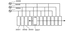
また、特許文献6では、図21のように、一定の間隔で並べられた矩形の送信電極3001、3002、3003にそれぞれ位相が互いに2π/3(120度)異なる3相の交流電圧3004、交流電圧3005および交流電圧3006を交互に印加し、送信電極に対面して移動する受信電極3007に誘起合成する電圧の位相を連続的に測定して精密な構造のノギスの測定精度を向上させている。
Further, in Patent Document 6, as shown in FIG. 21,
逆相すなわちπの位相差の交番電圧を使って電圧を検出する場合には、誘起電圧を増幅する増幅器の感度など電圧の測定精度が問題になる。また電圧をデジタル的に測定する場合には、A/Dコンバータの精度が問題になったり、A/Dコンバータを使うことにより構成が複雑になったりするという問題点がある。π/2や2π/3などの位相差の交番電圧を使って位相を検出する場合には、A/D変換をする必要がなく増幅器の感度なども問題にならないため、シンプルな構成で高精度な測定が行なえる。 In the case of detecting a voltage using an alternating voltage having a negative phase, that is, a phase difference of π, voltage measurement accuracy such as sensitivity of an amplifier that amplifies the induced voltage becomes a problem. Further, when the voltage is measured digitally, there is a problem that the accuracy of the A / D converter becomes a problem or the configuration becomes complicated by using the A / D converter. When detecting the phase using an alternating voltage with a phase difference such as π / 2 or 2π / 3, there is no need for A / D conversion and the sensitivity of the amplifier is not a problem. Measurement can be performed.
しかし、ノギスや、ロータリエンコーダなどに用いられている静電容量−位相変化方式を電子楽器で利用することは未だ提案されていない。また、ノギスや、ロータリエンコーダなどに用いられている静電容量−位相変化方式をそのまま電子楽器の鍵操作速度検出装置に利用することはできない。すなわち、ノギスやロータリエンコーダの場合には測定対象となる物体の位置や角度は1個しかないが、電子楽器の場合には88鍵などの多数の鍵を備えており、各鍵毎に独立して鍵の操作速度を検出する必要がある。これらの多数の鍵のそれぞれに対して交番電圧を発生する回路や電圧や位相を検出する回路を備えると複雑な構成となり高価なものとなってしまう。また、静電容量−位相変化方式の原理を説明するために用いた図20(b)の等価回路には、電極間の静電容量c1およびc2のみを示したが、実際には図20(b)に破線で示すように、受信電極から位相測定回路までの配線の浮遊容量や位相測定回路の入力容量などを合成した10pF程度の容量c3が存在する。このため位相測定回路に入力される電圧は、電極間静電容量c1およびc2と、容量c3とで分圧されたものとなる。位相測定回路に入力される電圧を充分なレベルにするためには電極間静電容量を大きくする必要がある。大きな容量を得るには、電極面積を大きく、電極間隙を小さく、電極間隙に空間を設けずに、誘電率の高い材料を挟めばよい。特許文献5に示された装置では、電極間に存在する円筒2002を誘電体とするとともに、円筒2002の内周面とロータ2004の外周面を接触させているため大きな電極間静電容量を容易に得ることができる。
However, it has not yet been proposed to use the capacitance-phase change method used in calipers, rotary encoders and the like in electronic musical instruments. In addition, the capacitance-phase change method used for calipers, rotary encoders, etc. cannot be used as it is for a key operation speed detection device of an electronic musical instrument. In other words, in the case of calipers and rotary encoders, there is only one position and angle of the object to be measured, but in the case of electronic musical instruments, there are many keys such as 88 keys, and each key is independent. It is necessary to detect the key operation speed. If a circuit for generating an alternating voltage and a circuit for detecting the voltage and phase are provided for each of these many keys, the configuration becomes complicated and expensive. In addition, in the equivalent circuit of FIG. 20B used for explaining the principle of the capacitance-phase change method, only the capacitances c1 and c2 between the electrodes are shown. As indicated by a broken line in b), there is a capacitance c3 of about 10 pF obtained by combining the floating capacitance of the wiring from the receiving electrode to the phase measurement circuit, the input capacitance of the phase measurement circuit, and the like. Therefore, the voltage input to the phase measuring circuit is divided by the interelectrode capacitances c1 and c2 and the capacitance c3. In order to set the voltage input to the phase measurement circuit to a sufficient level, it is necessary to increase the capacitance between the electrodes. In order to obtain a large capacity, a material having a high dielectric constant may be sandwiched between a large electrode area, a small electrode gap, and no space in the electrode gap. In the apparatus disclosed in Patent Document 5, the
ノギスや、ロータリエンコーダなどの場合には、このように電極間に誘電体を挟んで電極と誘電体を接触させながら電極を動かす構成をとっても大きな不具合とはならない。電子楽器の鍵操作速度検出に静電容量−位相変化方式を利用する場合には、送信電極(あるいは受信電極)を鍵操作に従って動かし、受信電極(あるいは送信電極)を送信電極に対向する位置に配置することが考えられるが、電極と誘電体を強く接触させながら電極を動かすようにすると、摩擦抵抗により鍵の操作感に影響を与えてしまう可能性がある。 In the case of a vernier caliper, a rotary encoder, or the like, even if the electrode is moved while the dielectric is sandwiched between the electrodes and the electrodes are in contact with each other, there is no serious problem. When the capacitance-phase change method is used to detect the key operation speed of the electronic musical instrument, the transmission electrode (or reception electrode) is moved according to the key operation, and the reception electrode (or transmission electrode) is moved to a position facing the transmission electrode. However, if the electrode is moved while the electrode and the dielectric are in strong contact with each other, the operation feeling of the key may be affected by the frictional resistance.
本発明は、従来の電子楽器の鍵操作速度検出装置の有している前述の問題を解決し、簡単な構成で正確に鍵操作速度を検出する装置を、提供するものである。 The present invention solves the above-mentioned problems of a conventional electronic musical instrument key operation speed detection device, and provides an apparatus for accurately detecting a key operation speed with a simple configuration.
前記課題を解決するために、請求項1記載の電子楽器の鍵操作速度検出装置は、
複数の鍵の各鍵に対応してそれぞれ1あるいは複数設けられた受信電極と、
前記受信電極と対向して配置された2個以上の送信電極と、
対応する鍵の押鍵操作によって前記受信電極または送信電極の何れかが移動して前記受信電極と送信電極間の静電容量が変化する鍵盤機構と、
複数の鍵に共通して設けられ、周期が同一でかつ位相が互いに異なる複数の交番信号を発生し、発生した各交番信号を前記各送信電極にそれぞれ供給するとともに、該交番信号と同じ周期の基準位相信号を発生する信号発生回路と、
複数の鍵に共通に設けられ、該複数の鍵の各鍵に設けられた前記受信電極に誘起された交番信号および前記基準位相信号が供給され、前記基準位相信号を用いて各鍵の受信電極に誘起された交番信号の位相を弁別することで該鍵の押圧深さを求め、鍵が少なくとも2個の押圧深さを通過する際の時間間隔を計測することで鍵の操作速度を求める信号処理回路と、
を備えるものである。
なお、前記の送信電極は、各鍵に個々に独立して設けられるものであってもよいし、複数の鍵に共通して設けられているものであってもよい。
In order to solve the above-mentioned problem, a key operation speed detection device for an electronic musical instrument according to
One or a plurality of receiving electrodes corresponding to each key of the plurality of keys;
Two or more transmitter electrodes disposed opposite the receiver electrodes;
A keyboard mechanism in which either the reception electrode or the transmission electrode is moved by pressing a corresponding key to change the capacitance between the reception electrode and the transmission electrode;
A plurality of alternating signals that are provided in common to a plurality of keys and have the same period and different phases are supplied to each of the transmission electrodes, and each of the generated alternating signals has the same period as the alternating signal. A signal generation circuit for generating a reference phase signal;
The alternating signal and the reference phase signal that are provided in common to a plurality of keys and are induced in the reception electrodes provided in the keys of the plurality of keys are supplied, and the reception electrodes of the keys are used by using the reference phase signal. A signal for determining the key pressing speed by determining the key pressing depth by discriminating the phase of the alternating signal induced in the key, and measuring the time interval when the key passes at least two pressing depths. A processing circuit;
Is provided.
The transmission electrode may be provided independently for each key, or may be provided in common for a plurality of keys.
請求項2記載の電子楽器の鍵操作速度検出装置は、請求項1に記載の電子楽器の鍵操作速度検出装置において、前記受信電極と前記送信電極との間には所定の間隙が設けられているものである。
An electronic musical instrument key operation speed detection device according to claim 2 is the electronic musical instrument key operation speed detection device according to
請求項3記載の電子楽器の鍵操作速度検出装置は、請求項2に記載の電子楽器の鍵操作速度検出装置において、
前記信号発生回路は、前記受信電極に誘起される交番信号の電圧が前記信号処理回路で処理可能なレベルになるように前記基準位相信号よりも高電圧の交番信号を前記送信電極に供給するものである。なお、前記の高電圧は昇圧トランスや高電圧ドライバを用いて発生することができる。
The key operation speed detecting device for an electronic musical instrument according to claim 3 is the key operation speed detecting device for an electronic musical instrument according to claim 2,
The signal generation circuit supplies an alternating signal having a voltage higher than that of the reference phase signal to the transmission electrode so that the voltage of the alternating signal induced at the reception electrode is at a level that can be processed by the signal processing circuit. It is. The high voltage can be generated using a step-up transformer or a high voltage driver.
請求項4記載の電子楽器の鍵操作速度検出装置は、請求項3に記載の電子楽器の鍵操作速度検出装置において、
前記送信電極、前記受信電極のいずれか、あるいは双方が絶縁膜で覆われているものである。
An electronic musical instrument key operation speed detection device according to
Either the transmission electrode, the reception electrode, or both are covered with an insulating film.
請求項5記載の電子楽器の鍵操作速度検出装置は、請求項3に記載の電子楽器の鍵操作速度検出装置において、
前記信号発生回路で発生する複数の交番信号を前記送信電極に供給する配線は、位相が互いにπ異なる交番信号を対として平行線あるいは撚り対線で前記送信電極に供給するものである。
The key operation speed detecting device for an electronic musical instrument according to claim 5 is the key operation speed detecting device for an electronic musical instrument according to claim 3,
The wiring for supplying a plurality of alternating signals generated by the signal generating circuit to the transmitting electrode supplies the alternating signals having a phase different from each other by a pair of parallel lines or twisted pair lines to the transmitting electrode.
請求項6記載の電子楽器の鍵操作速度検出装置は、請求項3に記載の電子楽器の鍵操作速度検出装置において、
前記信号発生回路で発生する複数の交番信号の位相は該複数の交番信号を加算したときに交番信号が相殺される位相に設定されているとともに、該複数の交番信号を前記送信電極に供給する配線は平行線、撚り対線、またはこれらの線をシールドで覆ったシールド線とすることで該配線からの不要輻射を相殺するものである。
The key operation speed detecting device for an electronic musical instrument according to claim 6 is the key operation speed detecting device for an electronic musical instrument according to claim 3,
The phases of the plurality of alternating signals generated in the signal generating circuit are set to phases that cancel the alternating signals when the plurality of alternating signals are added, and the plurality of alternating signals are supplied to the transmission electrode. The wiring is a parallel wire, a twisted pair wire, or a shielded wire in which these wires are covered with a shield, thereby canceling unnecessary radiation from the wiring.
請求項7記載の電子楽器の鍵操作速度検出装置は、請求項1に記載の電子楽器の鍵操作速度検出装置において、
前記受信電極は、各鍵に対応して複数設けられており、
前記送信電極は、2個設けられており、
前記信号発生回路は、2個の送信電極に位相が互いにπ異なる2個の交番信号をそれぞれ供給するものであり、
前記信号処理回路は、各鍵の少なくとも2つの受信電極からの交番信号が位相反転する時間間隔から鍵の操作速度を求めるものである。
The key operation speed detecting device for an electronic musical instrument according to claim 7 is the key operation speed detecting device for an electronic musical instrument according to
A plurality of the receiving electrodes are provided corresponding to each key,
Two transmission electrodes are provided,
The signal generation circuit supplies two alternating signals having phases different from each other by π to the two transmission electrodes,
The signal processing circuit obtains the key operation speed from the time interval at which the alternating signals from at least two receiving electrodes of each key are phase-inverted.
請求項8記載の電子楽器の鍵操作速度検出装置は、請求項1に記載の電子楽器の鍵操作速度検出装置において、
前記受信電極は、各鍵に対応して1個設けられており、
前記送信電極は、2個以上設けられており
前記信号処理回路は、各鍵の受信電極からの前記交番信号の位相が少なくとも2つの所定の位相と同一になった際の時間間隔から鍵の操作速度を求めるものである。
The key operation speed detecting device for an electronic musical instrument according to claim 8 is the key operation speed detecting device for an electronic musical instrument according to
One receiving electrode is provided corresponding to each key,
Two or more transmission electrodes are provided, and the signal processing circuit operates the key from the time interval when the phase of the alternating signal from the reception electrode of each key is the same as at least two predetermined phases. It is for speed.
請求項9記載の電子楽器の鍵操作速度検出装置は、請求項1に記載の電子楽器の鍵操作速度検出装置において、
前記鍵あるいは該鍵に連動する部材に前記送信電極が設けられているとともに、前記鍵盤機構の基部に前記受信電極および前記信号処理回路が設けられているものである。
The key operation speed detecting device for an electronic musical instrument according to claim 9 is the key operation speed detecting device for an electronic musical instrument according to
The transmission electrode is provided on the key or a member interlocking with the key, and the reception electrode and the signal processing circuit are provided on a base portion of the keyboard mechanism.
請求項10記載の電子楽器の鍵操作速度検出装置は、請求項1に記載の電子楽器の鍵操作速度検出装置において、
前記鍵あるいは該鍵に連動する部材に前記受信電極が設けられているとともに、前記鍵盤機構の基部に前記送信電極および前記信号発生回路が設けられているものである。
The key operation speed detection device for an electronic musical instrument according to
The receiving electrode is provided on the key or a member interlocking with the key, and the transmitting electrode and the signal generating circuit are provided on the base of the keyboard mechanism.
請求項11記載の電子楽器の鍵操作速度検出装置は、請求項10に記載の電子楽器の鍵操作検出装置において、
前記受信電極に誘起された交番信号を前記信号処理回路に供給する配線にグランドラインで挟まれたシールドが施されているものである。
An electronic musical instrument key operation speed detecting device according to claim 11 is the electronic musical instrument key operation speed detecting device according to
A shield that is sandwiched between ground lines is provided on a wiring that supplies an alternating signal induced to the receiving electrode to the signal processing circuit.
請求項1に記載の装置によれば、信号発生回路で発生した交番信号を複数の鍵で共通して使用するとともに1つの信号処理回路で複数の鍵の操作速度、深さを求めるため、簡単な構成で正確に鍵操作速度を検出することができる。
According to the apparatus of
請求項2記載に記載の装置によれば、請求項1に記載の装置の奏する効果に加え、送信電極と受信電極との間に間隙が設けられているため鍵の操作感に影響を与えることがない。 According to the device of the second aspect, in addition to the effect produced by the device of the first aspect, since the gap is provided between the transmission electrode and the reception electrode, the operational feeling of the key is affected. There is no.
請求項3に記載の装置によれば、請求項2に記載の装置の奏する効果に加え、送信電極によって強い電界を発生することで、送信電極と受信電極との間に空間を設けながら受信電極に誘起される交番信号の電圧が信号処理回路で処理可能なレベルとすることができ、非接触で、かつ安定して鍵操作速度、深さを検出することができる。 According to the device of claim 3, in addition to the effect of the device of claim 2, the receiving electrode generates a strong electric field by the transmitting electrode, thereby providing a space between the transmitting electrode and the receiving electrode. The voltage of the alternating signal induced in the signal can be set to a level that can be processed by the signal processing circuit, and the key operation speed and depth can be detected stably without contact.
請求項4に記載の装置によれば、請求項3に記載の装置の奏する効果に加え、送信電極に絶縁膜を施した場合には送信電極によって強い電界を発生しても、高湿度や塵埃の多い環境での電極間の漏洩電流や放電を阻止し、受信電極に絶縁膜を施した場合には受信電極に誘起された信号の漏洩を阻止し、安定して鍵操作速度を検出することができる。
According to the device according to
請求項5に記載の装置によれば、請求項3に記載の装置の奏する効果に加え、送信電極によって強い電界を発生しても、信号発生回路から送信電極までの長い配線からの不要輻射を相殺して、信号発生回路を複数の鍵で共有し、安価な装置を提供できる。 According to the device of the fifth aspect, in addition to the effect of the device of the third aspect, even if a strong electric field is generated by the transmission electrode, unnecessary radiation from a long wiring from the signal generation circuit to the transmission electrode is prevented. By canceling out, it is possible to share the signal generation circuit with a plurality of keys and provide an inexpensive device.
請求項6に記載の装置によれば、請求項3に記載の装置の奏する効果に加え、送信電極によって強い電界を発生しても、信号発生回路から送信電極までの長い配線からの不要輻射を相殺して、信号発生回路を複数の鍵で共有し、安価な装置を提供できる。 According to the device of the sixth aspect, in addition to the effect produced by the device of the third aspect, even if a strong electric field is generated by the transmission electrode, unwanted radiation from a long wiring from the signal generation circuit to the transmission electrode is prevented. By canceling out, it is possible to share the signal generation circuit with a plurality of keys and provide an inexpensive device.
請求項7に記載の装置によれば、請求項1に記載の装置の奏する効果に加え、簡単な構成で受信電極からの交番信号の位相を弁別してその受信電極が2個の送信電極の中間に位置したことが検出でき、少なくとも2個の受信電極からの交番信号の位相反転の時間間隔から鍵の操作速度を求めることができる。
According to the device according to claim 7, in addition to the effect of the device according to
請求項8に記載の装置によれば、請求項1に記載の装置の奏する効果に加え、簡単な構成で受信電極からの交番信号の位相を弁別することができ、交番信号の位相が所定の変化をする時間間隔から鍵の操作速度を求めることができる。また、請求項8に記載の装置によれば交番信号の位相を弁別することで、鍵の操作速度を求めるだけでなく同時に鍵操作の深さを求めることもできる。
According to the device according to claim 8, in addition to the effect of the device according to
請求項9に記載の装置によれば、請求項1に記載の装置の奏する効果に加え、同じ部材に受信電極と信号処理回路が設けられているため、受信電極から信号処理回路までの配線を短くすることができ、受信電極に誘起された交番信号を有効に信号処理回路に導くことができる。 According to the device of the ninth aspect, in addition to the effect produced by the device of the first aspect, since the reception electrode and the signal processing circuit are provided on the same member, the wiring from the reception electrode to the signal processing circuit is provided. The alternating signal induced in the receiving electrode can be effectively guided to the signal processing circuit.
請求項10記載の装置によれば、請求項1に記載の装置の奏する効果に加え、信号発生回路から送信電極までの距離を短くでき、かつ、小さな受信電極は大きな振幅で移動できるため、鍵盤機構を小型化できる。
According to the device of
請求項11記載の装置によれば、請求項10に記載の装置の奏する効果に加え、受信電極から信号処理回路までの配線に周辺の空間からの妨害電波が乗るのを防ぐことができる。 According to the device of the eleventh aspect, in addition to the effect produced by the device of the tenth aspect, it is possible to prevent the interference wave from the surrounding space from getting on the wiring from the receiving electrode to the signal processing circuit.
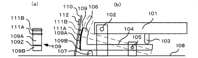
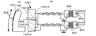
以下、本発明の好ましい第1の実施の形態について、添付図面を参照して説明する。図1は、本発明が適用された電子楽器の鍵操作速度検出装置における鍵、ハンマー、送信電極、受信電極の関係を示している。代表として1つの鍵を取り上げて説明するが、他の鍵でも同様に構成されている。図1(a)には電極をハンマーの先端部の正面側から見た図が示されており、図1(b)には鍵の機構を側面から見た図が示されている。 Hereinafter, a preferred first embodiment of the present invention will be described with reference to the accompanying drawings. FIG. 1 shows a relationship among a key, a hammer, a transmission electrode, and a reception electrode in a key operation speed detection device for an electronic musical instrument to which the present invention is applied. One key will be described as a representative, but the other keys are similarly configured. FIG. 1A shows the electrode viewed from the front side of the tip of the hammer, and FIG. 1B shows the key mechanism viewed from the side.
演奏者が鍵101を押下すると、鍵101は回動軸102を中心に回動する。鍵101に連動してジャック103がハンマー104を動かし、ハンマー104は回動軸105を中心に回動し、ハンマー104の先端部106は上に上がる。演奏者の離鍵操作により鍵101は図示しないバネなどにより元の位置に復帰し、ハンマー104は自重により元の位置に復帰し、受け部材107に当接する。これらの鍵機構は鍵盤基部108の上に構築されている。
When the performer depresses the key 101, the key 101 rotates about the
ハンマー104の先端部106には送信電極109が配置されている。送信電極109は、何れも矩形の第1の送信電極109Aおよび第2の送信電極109Bから構成されており、第1の送信電極109Aおよび第2の送信電極109Bは、ハンマー104の移動方向に沿って所定の間隔109Zをおいて先端部106に絶縁固定されている。送信電極109のハンマー104の移動方向に対する長さは、第1の送信電極109Aの方が第2の送信電極109Bよりも長くなっており、また第1の送信電極109Aが上に、第2の送信電極109Bが下に配置されている。両送信電極の幅(ハンマー104の移動方向に垂直な方向の長さ)はハンマー104の幅とほぼ同じとされている。両送信電極109Aおよび109Bには後述するように高電圧がかけられるため、漏電や放電を防止するように電極表面および間隔109Zに絶縁膜が施されているのが望ましい。
A
鍵盤基部108のハンマー104の先端部106に対向する位置に速度検出基板110が設置されている。速度検出基板110には何れも矩形の第1の受信電極111Aおよび第2の受信電極111Bがハンマー104の移動方向に沿って所定の間隔をおいて印刷または装着されているとともに、論理集積回路112が装着されている。受信電極111Aおよび受信電極111Bは、ハンマー104が回動したときに送信電極109Aおよび送信電極109Bと接触しないように所定の間隙を設けて、これらの電極に対向する位置に近接して配置されている。なお、ハンマー104の先端部106の受信電極と対向する面は、ハンマー104が回動したときに送信電極と受信電極との距離が変化しないように、回動曲線に沿って湾曲している。受信電極のハンマー104の移動方向の長さは送信電極の局所的な影響のみを受けるように何れの送信電極よりも短くされており、受信電極のハンマー104の移動方向に垂直方向の幅は送信電極の幅とほぼ同じとしている。また、受信電極111Aが上に、第2の受信電極111Bが下に配置されており、押鍵がなされていない状態においては両受信電極とも第1の送信電極109Aと対向している。押鍵がなされると、ハンマー104の先端106は上方に移動し、送信電極109Aに続いて送信電極109Bが各受信電極の近傍を通過する。なお、受信電極には、誘起された信号の漏洩を阻止するために電極表面および隣接する電極間に絶縁膜が施されているのが望ましい。
A
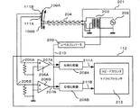
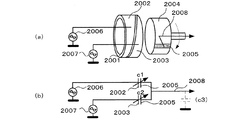
図2は、送信電極に印加する信号を発生する信号発生回路201および受信電極に誘起された信号を処理する論理集積回路112の内部構成を示している。信号発生回路201は正弦波発振器202および平衡昇圧トランス203から構成されており、鍵盤基部108に備えられている。正弦波発振器202は100kHzの長波帯の正弦波交番信号を生成する。生成された信号は平衡昇圧トランス203によって高電圧に昇圧される。なお、正弦波発振器202の出力の一端はグランドに接続されている。平衡昇圧トランス203の2次側のセンタータップはグランドに接続されており、平衡昇圧トランス203の2次側の両端の端子からは電圧が等しく位相が互いにπ異なる(逆相)2相の高圧交番信号が出力される。平衡昇圧トランス203の昇圧比については後述する。ここでは1つの鍵のみを代表して示したが、信号発生回路201は複数の鍵に共通で使用され、信号発生回路201からの高圧の交番信号を複数の鍵の送信電極に供給する。
FIG. 2 shows an internal configuration of a
配線204は、配線204からの不要輻射を減らすために平行線、撚り対線、あるいは、平行線あるいは撚り対線とされた芯線をシールドでガードした(覆った)シールド線とするのが望ましい。配線204を平行線あるいは撚り対線としておけば、配線204を通る信号は互いに逆相であるため互いに相殺され、不要輻射は低減される。シールド線にした場合には、配線204からの不要輻射はさらに低減される。配線204からの不要輻射は平行線、撚り対線、シールド線の順に小さくなるが、配線204の構造は許容される不要輻射の大きさ、コスト等を勘案して決めればよい。なお、配線204としてシールド線を使う場合には、図2に示すように配線204のシールドはグランドに接続する。なお、平衡昇圧トランス203は鍵盤基部108に備えられており、送信電極109はハンマー104に設けられているため、配線204のうちハンマー104に信号を受け渡す箇所はハンマー104の動作を妨げることがないよう柔軟性に富んだ線材を使用するのが望ましい。
In order to reduce unnecessary radiation from the
送信電極109Aに印加された交番信号が、送信電極109Aと受信電極111A、受信電極111Bとの間に形成された静電容量を介して受信電極111A、受信電極111Bに誘起される。同様に送信電極109Bに印加された交番信号も、送信電極109Bと受信電極111A、受信電極111Bとの間に形成された静電容量を介して受信電極111A、受信電極111Bに誘起される。これらの静電容量はハンマー104の移動に伴って変化する。受信電極111A、受信電極111Bに誘起された交番信号は論理集積回路112に供給される。受信電極111Aおよび受信電極111Bから論理集積回路112までの配線は図示しないシールドやガード用の銅箔で囲んで隣接する配線からのクロストークや雑音の混入を防ぐようになされている。論理集積回路112については後に詳解する。
An alternating signal applied to the
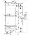
図3には複数の鍵の送信電極、受信電極および論理集積回路112までの等価回路が示されている。コンデンサc1は送信電極109Aと受信電極111Aあるいは111Bとの間に形成された静電容量、コンデンサc2は送信電極109Bと受信電極111Aあるいは111Bとの間に形成された静電容量、コンデンサc3は論理集積回路112の入力容量、コンデンサc4は速度検出基板110上の隣接する受信電極の配線との間の浮遊容量で前記クロストークの原因となる。コンデンサc5は受信電極から論理集積回路112までの配線の浮遊容量をそれぞれ示している。コンデンサc1およびコンデンサc2の容量は、電極のサイズ、電極間の距離にもよるが、最大でも1pFに満たず、コンデンサc3の容量は概ね5pF程度となる。前述したように受信電極から論理集積回路112までの配線をシールドやガード用の銅箔で囲んだ場合には、コンデンサc4は小さくなり、c5は大きくなる。送信電極109Aおよび送信電極109Bにかけられる交番信号をそれぞれe1およびe2とすると論理集積回路112に入力される電圧は、
《数2》
V=(e1*c1+e2*c2)/(c1+c2+c3+c5) 式2
となる。コンデンサc3とc5の容量はコンデンサc1およびコンデンサc2の容量よりも1桁以上大きいので、論理集積回路112に入力される電圧は送信電極にかけられる電圧の数10分の1となる。このため、平衡昇圧トランス203の昇圧比をコンデンサc3、c5の容量とコンデンサc1およびコンデンサc2の容量の比程度に設定する。このように送信電極にかける電圧を高い電圧とすることで、送信電極と受信電極との間に形成される静電容量が小さくても、論理集積回路112でデジタル処理するのに十分なレベルの信号を得ることができる。
FIG. 3 shows a plurality of key transmission electrodes, reception electrodes, and an equivalent circuit up to the logic integrated
<< Equation 2 >>
V = (e1 * c1 + e2 * c2) / (c1 + c2 + c3 + c5) Equation 2
It becomes. Since the capacities of the capacitors c3 and c5 are larger by one digit or more than the capacities of the capacitors c1 and c2, the voltage input to the logic integrated
なお、図3には示していないが、平衡昇圧トランス203の2次側から送信電極109A、送信電極109Bまでの配線には浮遊容量が存在するとともに、送信電極109A、送信電極109Bとグランドとの間にも浮遊容量が存在する。従って、平衡昇圧トランス203の2次側には、これらの浮遊容量が接続された鍵の数の分だけ加算されて負荷となる。平衡昇圧トランス203の1次側と、2次側の両端間の巻数比をnとすると、平衡昇圧トランス203の1次側から見た前述の浮遊容量の値は、2次側の浮遊容量のnの二乗倍となる。nの二乗倍となった浮遊容量と平衡昇圧トランス203の1次側のインダクタンスによって共振回路が形成される。この共振回路の共振周波数が正弦波発振器202の発生する交番信号の周波数と一致するように、平衡昇圧トランス203のコイルを設計するのが望ましい。このようにすると、平衡昇圧トランス203の1次側から見たインピーダンスが高くなるために、平衡昇圧トランス203の1次側に流れる電流を少なくすることができる。このため昇圧における電力効率が向上し平衡昇圧トランスを小型化することができる。 また、このようにすると、平衡昇圧トランス203の1次側の信号と2次側の信号の位相差を最少にすることができ、位相の測定結果の誤差を小さくすることができる。ただし、共振回路の共振周波数と正弦波発振器の発生する交番信号の周波数を正確に同調させて、平衡昇圧トランスによって位相ずれが生じないようにしなければならない。なお、電極に印加する高電圧の交番信号は昇圧トランスの代わりに高電圧ドライバを用いた増幅回路を使用して生成するようにしてもよい。高電圧ドライバを用いた増幅回路を使用した場合には、前述の共振回路の同調の必要性はない。
Although not shown in FIG. 3, there is a stray capacitance in the wiring from the secondary side of the balanced step-up
なお、前記の静電容量c5は受信電極から論理集積回路112までの配線の浮遊容量であるので、この配線の長さによって容量の大きさが決まる。1個の論理集積回路112が多数の鍵の速度検出を受け持つ場合、つまり速度検出基板110上の受信電極端子111Aおよび受信電極端子111Bから論理集積回路112の入力端子までのそれぞれの導線の長さが鍵によって大きく異なる場合は、鍵によって静電容量c5の大きさが大きく異なることとなる。この場合には、前記受信電極端子111Aおよび受信電極端子111Bの近傍で安価なCMOSインバータなどの比較的増幅度の小さいバッファーで中継して導線の静電容量c5を最小にし、導線間クロストークや外来雑音による影響を低減してもよい。
Since the capacitance c5 is a stray capacitance of the wiring from the receiving electrode to the logic integrated
図2に戻り、受信電極111Aおよび受信電極111Bに誘起された検出信号205Aおよび検出信号205Bは論理集積回路112に供給されて、それぞれ電圧比較器206Aおよび電圧比較器206Bの正側入力端子に入力される。電圧比較器206Aおよび電圧比較器206Bの正側入力端子とグランドとの間には数MΩ程度の抵抗が接続されており、電圧比較器206Aおよび電圧比較器206Bの負側入力端子はグランドに接続されている。電圧比較器206Aおよび電圧比較器206Bは正側入力端子の電圧が負側入力端子の電圧よりも高い場合には“1”を出力し、正側入力端子の電圧が負側入力端子の電圧よりも低い場合には“0”を出力することで、検出信号205Aおよび検出信号205Bをそれぞれ論理レベルに変換し、位相パルス207Aおよび位相パルス207Bとする。
Returning to FIG. 2, the
位相パルス207Aおよび位相パルス207Bはそれぞれ次段の位相比較器208Aおよび位相比較器208Bに送出される。一方、正弦波発振器202からの信号がレベルコンバータ209で論理レベルに変換されて基準位相信号210とされ、位相比較器208Aおよび位相比較器208Bに送出される。位相比較器208Aは位相パルス207Aと基準位相信号210との排他的論理和をとって位相出力211Aとしてマイクロプロセッサ212に供給する。同様に位相比較器208Bは位相パルス207Bと基準位相信号210との排他的論理和をとって位相出力211Bとしてマイクロプロセッサ212に供給する。
The
マイクロプロセッサ212は位相出力211Aおよび位相出力211Bに基づいて、ノートオンと判別したときには、押鍵速度情報を含むノートオン指示を図示しない音源に送出するとともに、ノートオフと判別したときには、離鍵速度情報を含むノートオフ指示を音源に送出する。
Based on the
なお、論理集積回路112は1オクターブ程度の複数の鍵毎に1つ設け、1つの論理集積回路112で複数の鍵についての処理を行う。このとき、論理集積回路112内のマイクロプロセッサ212以外の構成要素は各鍵に独立して用意するが、マイクロプロセッサ212は1つのみ設け、1つのマイクロプロセッサ212で複数の鍵についての処理を行う。あるいは、論理集積回路112内にマイクロプロセッサ212以外の構成要素のみを設け、マイクロプロセッサ212は論理集積回路112とは別の部品としてもよい。この場合には複数の論理集積回路112と1つのマイクロプロセッサ212を接続し、1つのマイクロプロセッサ212で複数の論理集積回路112に対する処理を行うようにする。
One logic integrated
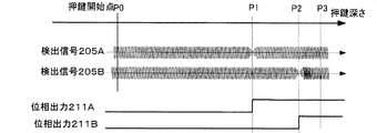
図4には、押鍵深さが変化したときの検出信号205A、検出信号205B、位相出力211A、位相出力211Bが示されている。図5には、図4に示される検出信号205A、位相パルス207A、基準位相信号210および位相出力211Aの関係が押鍵深さ方向に拡大して示されている。押鍵開始点P0は鍵の初期位置、すなわちまだ押鍵されていない状態での押鍵深さを示している。押鍵深さP1は受信電極111Aが送信電極109Aおよび送信電極109Bの境界に位置する深さを示している。押鍵深さP2は受信電極111Bが送信電極109Aおよび送信電極109Bの境界に位置する深さを示している。押鍵深さP3は最も深い位置まで押鍵されたときの位置を示している。
FIG. 4 shows a
押鍵開始点P0では、受信電極111Aおよび受信電極111Bはいずれも送信電極109Aが対向しているため、受信電極111Aおよび受信電極111Bの両方に送信電極109Aの交番信号が定常的に誘起している。このとき位相パルス208Aと基準位相信号210とは同位相であるため、位相比較器206Aで排他的論理和をとった結果の位相出力211Aは“0”となっている。同様に位相出力211Bも“0”となっている。
At the key press start point P0, since the receiving
押鍵されて押鍵深さが図4に示す第1の押鍵深さP1に近づくと、送信電極109Aが受信電極111Aに与える影響が小さくなり、逆に送信電極109Bが受信電極111Aに与える影響が大きくなるため、送信電極109Aによって印加される信号が送信電極109Bによって印加される逆相の信号によって減殺され、受信電極111Aに誘起合成される信号の振幅は急激に減少する。
When the key is depressed and the key depression depth approaches the first key depression depth P1 shown in FIG. 4, the influence of the
押鍵深さが図4に示す第1の押鍵深さP1に到達したときには、受信電極111Aが送信電極109Aと送信電極109Bの境界に位置し、受信電極111Aへの二つの送信電極からの影響が等しくなるため、受信電極111Aに誘起合成される信号は相殺して“0”となる。この一瞬、交番信号10のレベルが“0”となるため位相は不確定となる。
When the key pressing depth reaches the first key pressing depth P1 shown in FIG. 4, the receiving
押鍵深さが第1の押鍵深さP1を過ぎると、受信電極111Aに与える送信電極109Aの影響が小さくなるとともに、送信電極109Bの影響が大きくなるため、誘起電圧は急速に増大し、かつ位相は明確に反転し、位相出力211Aは“0”から“1”に変化する。
When the key depression depth exceeds the first key depression depth P1, the influence of the
押鍵がさらに進んで送信電極109Aと送信電極109Bの境界が受信電極111Bの上を通過して行き、前述の場合と同様にして押鍵深さが第2の押鍵深さP2を通過すると、位相出力211Bが“0”から“1”に変化する。
When the key depression further proceeds, the boundary between the
このようにして得られた位相出力211Aと位相出力211Bの“0”から“1”に変化するタイミングの時間差、つまり押鍵深さが第1押鍵深さP1から第2の押鍵深さP2に遷移する際の時間差を、マイクロプロセッサ212のプログラムによるスピードカウンタによって計測し、これから押鍵速度を求めることができる。この時間差は数ミリ秒のオーダーなので10マイクロ秒周期の基準位相信号210を計数するようにしてもよい。
The time difference between the timings when the
図6には、マイクロプロセッサ212の処理内容が示されている。実際には複数の鍵の処理が時分割で行われるがここでは説明を簡略化するために1つの鍵についてのみ解説する。この処理は充分に短い一定時間毎に繰り返し起動される。また処理に使う変数は図示しない処理により電源投入時に初期化されている。
FIG. 6 shows the processing contents of the
ステップS101では、位相出力211Aの前回の処理からのレベル変化を判別する。なお、位相出力211Aの前回の処理におけるレベルは後述するステップS110において記憶されている。現在のレベルが“0”で前回の処理と変化していない場合にはステップS110に進み、レベルが“0”から“1”に変化した場合にはステップS102に進み、レベルが“1”から“0”に変化した場合にはステップS104に進み、レベルが“1”で前回の処理と変化していない場合にはステップS108に進む。
In step S101, the level change from the previous processing of the
ステップS102では、押鍵速度カウンタの値をクリアして、ステップS103に進む。ステップS103では、押鍵速度カウンタのカウントを開始し、ステップS110に進む。 In step S102, the value of the key pressing speed counter is cleared, and the process proceeds to step S103. In step S103, the key pressing speed counter starts counting, and the process proceeds to step S110.
ステップS104では、離鍵速度カウンタのカウント中であるか判断し、カウント中である場合にはステップS105に進み、カウント中でない場合にはステップS110に進む。ステップS105では、離鍵速度カウンタのカウントを停止して、ステップS106に進む。ステップS106では、離鍵速度カウンタのカウント値から離鍵速度を算出してステップS107に進む。ステップS107では、離鍵速度情報を含むノートオフ指示を音源に送出しするステップS110に進む。 In step S104, it is determined whether the key release speed counter is being counted. If it is being counted, the process proceeds to step S105, and if it is not being counted, the process proceeds to step S110. In step S105, the count of the key release speed counter is stopped, and the process proceeds to step S106. In step S106, the key release speed is calculated from the count value of the key release speed counter, and the process proceeds to step S107. In step S107, the process proceeds to step S110 in which a note-off instruction including key release speed information is sent to the sound source.
ステップS108では、押鍵速度カウンタのカウント中であるか判断し、カウント中である場合にはステップS109に進み、カウント中でない場合にはステップS110に進む。ステップS109では、押鍵速度カウンタの値をインクリメントし、ステップS110に進む。 In step S108, it is determined whether the key pressing speed counter is being counted. If it is being counted, the process proceeds to step S109, and if it is not being counted, the process proceeds to step S110. In step S109, the value of the key pressing speed counter is incremented, and the process proceeds to step S110.
ステップS110では、位相出力211Aのレベルを記憶し、ステップS111に進む。
In step S110, the level of the
ステップS111では、位相出力211Bの前回の処理からのレベル変化を判別する。なお、位相出力211Bの前回の処理におけるレベルは後述するステップS120において記憶されている。現在のレベルが”0“で前回の処理と変化していない場合にはステップS112に進み、レベルが“0”から“1”に変化した場合にはステップS114に進み、レベルが“1”から“0”に変化した場合にはステップS118に進み、レベルが“1”で前回の処理と変化していない場合にはステップS120に進む。
In step S111, the level change from the previous process of the
ステップS112では、離鍵速度カウンタのカウント中であるか判断し、カウント中である場合にはステップS113に進み、カウント中でない場合にはステップS120に進む。ステップS113では、離鍵速度カウンタの値をインクリメントし、ステップS120に進む。 In step S112, it is determined whether the key release speed counter is being counted. If it is being counted, the process proceeds to step S113, and if it is not being counted, the process proceeds to step S120. In step S113, the value of the key release speed counter is incremented, and the process proceeds to step S120.
ステップS114では、押鍵速度カウンタのカウント中であるか判断し、カウント中である場合にはステップS115に進み、カウント中でない場合にはステップS120に進む。ステップS115では、押鍵速度カウンタのカウントを停止して、ステップS116に進む。ステップS116では、押鍵速度カウンタのカウント値から押鍵速度を算出して、ステップS117に進む。ステップS117では、押鍵速度情報を含むノートオン指示を音源に送出し、ステップS120に進む。 In step S114, it is determined whether the key pressing speed counter is being counted. If it is being counted, the process proceeds to step S115, and if it is not being counted, the process proceeds to step S120. In step S115, the count of the key pressing speed counter is stopped, and the process proceeds to step S116. In step S116, the key pressing speed is calculated from the count value of the key pressing speed counter, and the process proceeds to step S117. In step S117, a note-on instruction including key pressing speed information is sent to the sound source, and the process proceeds to step S120.
ステップS118では、離鍵速度カウンタの値をクリアしてステップS119に進む。ステップS119では、離鍵速度カウンタのカウントを開始しステップS120に進む。 In step S118, the value of the key release speed counter is cleared, and the process proceeds to step S119. In step S119, the key release speed counter starts counting, and the process proceeds to step S120.
ステップS120では位相出力211Bのレベルを記憶して処理を終了する。
In step S120, the level of the
押鍵が未だなされておらず押鍵深さが押鍵開始点P0にあるときには、位相出力211Aおよび位相出力211Bのレベルは“0”であり、押鍵速度カウンタのカウント中でも離鍵速度カウンタのカウント中でもないため、ステップS101、ステップS110、ステップS111、ステップS112、ステップS120の処理を行い、その時点の位相出力を記憶する処理のみを行う。押鍵が開始されても押鍵深さが第1の押鍵深さP1に達するまでは位相出力211Aおよび位相出力211Bのレベルは変化しないため同様の処理を繰り返す。
When the key is not yet pressed and the key pressing depth is at the key pressing start point P0, the levels of the
押鍵深さが第1の押鍵深さP1に達したときには、位相出力211Aのレベルが“0”から“1”に変化するので、ステップS102、ステップS103の処理が行われて押鍵速度のカウントが開始される。押鍵速度のカウント中で押鍵深さが第1の押鍵深さP1と第2の押鍵深さP2の間にあるときには、位相出力211Aのレベルは“1”であるのでステップS109の処理によって押鍵速度カウンタの値がインクリメントされる。
When the key pressing depth reaches the first key pressing depth P1, the level of the
押鍵が進み押鍵深さが第2の押鍵深さP2に達したときには、位相出力211Bのレベルが“0”から“1”に変化するので、ステップS114〜ステップS117の処理が行われて、押鍵速度カウントが停止され、押鍵速度カウンタのカウント値から押鍵速度が算出されて、音源に押鍵速度情報を含むノートオン指示が出力される。押鍵深さが第2の押鍵深さP2を越しているときには、位相出力211Aおよび位相出力211Bのレベルは“1”であり、押鍵速度カウンタおよび離鍵速度カウンタのカウント中ではないため、ステップS101、ステップS110、ステップS111およびステップS120によってその時点の位相出力を記憶する処理のみを行う。
When the key press advances and the key press depth reaches the second key press depth P2, the level of the
離鍵が開始され押鍵深さが第2の押鍵深さP2に達したときには、位相出力211Bのレベルが“1”から“0”に変化するので、ステップS118、ステップS119の処理が行われて、離鍵速度のカウントが開始される。離鍵速度のカウント中で押鍵深さが第2の押鍵深さP2と第1の押鍵深さP1の間にあるときには、位相出力211Bのレベルは“0”であるので、ステップS113の処理によって離鍵速度カウンタの値がインクリメントされる。
When the key release is started and the key pressing depth reaches the second key pressing depth P2, the level of the
離鍵が進み押鍵深さが第1の押鍵深さP1に達したときには、位相出力211Aのレベルが“1”から“0”に変化するので、ステップS104〜ステップS107の処理が行われて、離鍵速度カウントが停止され、離鍵速度カウンタのカウント値から離鍵速度が算出されて、音源に離鍵速度情報を含むノートオフ指示が出力される。
When the key release progresses and the key pressing depth reaches the first key pressing depth P1, the level of the
このように本実施の形態によれば電圧が平衡し、位相が逆の交番信号が印加された2つの送信電極の境界が受信電極の近傍を通過することによる急激な位相の変化を検出して、正確な押鍵の深さを検出することができる。温度や機構精度のバラつきなどで電極隙間が変動すると、静電容量が変化し検出電圧の変動をもたらすが、位相検出なら受信電極に誘起する信号の電圧ではなく、誘起する信号の急速な位相変化を検出するため検出電圧の影響を最小限に留めることがでる。 As described above, according to the present embodiment, a sudden phase change is detected by the fact that the boundary between two transmission electrodes to which an alternating signal having an opposite phase is applied and a voltage is balanced passes through the vicinity of the reception electrode. It is possible to detect the exact key pressing depth. If the electrode gap fluctuates due to variations in temperature or mechanism accuracy, the capacitance changes, causing fluctuations in the detection voltage. Therefore, the influence of the detection voltage can be minimized.
従来の1個の送信電極と1個の受信電極を用いた誘導電圧検出による鍵操作速度検出方式では、アナログ量の値を求めるための高価なA/Dコンバータなどが必要になるが、本発明では簡単なデジタル位相比較器を用いて鍵操作速度検出装置を小規模の集積回路で構成することができる。また、従来の誘導電圧検出による鍵操作速度検出方式では、温度や機構精度のバラつきなどによる検出電圧の変化が鍵操作速度の検出精度に影響を与えるが、本発明では検出電圧の変化の影響を受けることなく正確な鍵操作速度検出を行なえる。また本実施の形態によれば、送信電極に交番信号を付与するための1個の信号発生回路201を複数の鍵で共用しているとともに、受信電極に誘起された交番信号の位相を判別するための論理集積回路112も複数の鍵で共用しているため、簡単な構成で鍵操作速度を検出することができる。また本実施の形態によれば、送信電極と受信電極との間に間隙が設けられているため、鍵の操作感に影響を与えることがない。
In the conventional key operation speed detection method based on induction voltage detection using one transmission electrode and one reception electrode, an expensive A / D converter or the like for obtaining an analog value is required. Then, the key operation speed detecting device can be constituted by a small scale integrated circuit using a simple digital phase comparator. In addition, in the conventional key operation speed detection method based on induced voltage detection, the change in detection voltage due to variations in temperature and mechanism accuracy affects the detection accuracy of the key operation speed. Accurate key operation speed detection can be performed without receiving it. Further, according to the present embodiment, one
なお、受信電極のハンマー104の移動方向の長さを長くすると、受信電極が2つの送信電極の境界を通過する際に受信電極に誘起される信号の位相遷移が緩やかになる。これは受信電極に誘起される信号が、受信電極と対向する各送信電極の面積の比率に従って定まるためである。このため、受信電極のハンマー104の移動方向の長さを長くすると空間分解能は下がる。一方、受信電極のハンマー104の移動方向の長さを長くすると受信電極に誘起される信号のレベルは上がる。どの程度の長さにするかは、鍵盤機構の精度とのトレードオフとなる。また、この実施の形態では、送信電極と受信電極との間に間隙が設けられているため、鍵の操作感に影響を与えることがないが、送信電極と受信電極との間に誘電体を挟んで電極間の距離を縮めても両電極が接触するのを防止するようにしてもよい。この場合、両電極の間に1つの誘電体を挟んだり、あるいは各電極の表面をそれぞれ誘電体で覆ったりする構成が考えられるが、いずれの場合も電極が誘電体に接触しながら移動したり誘電体同士が接触しながら移動したりする可能性があるので、鍵の操作感に与える影響を最小限にするために摩擦係数の小さな誘電体を用いるのが望ましい。
If the length of the receiving electrode in the moving direction of the
次に、本発明の好ましい第2の実施の形態について説明する。ピアノのような打弦楽器はハンマーが弦を打撃する瞬間、つまりハンマーの最終速度によって音量や音色が決定されるが、電子楽器の場合はピアノとは機構が異なるため電子楽器のハンマーの最終速度はピアノのハンマーの最終速度と異なる場合がある。このため、電子楽器では鍵やハンマーの最終速度に加えて初速度も検出して、発音を制御する場合がある。また高速で連打する場合は、鍵やハンマーが初期位置に復帰する前に次の押鍵がなされる場合がある。このため従来の鍵スイッチを用いる方式では、鍵スイッチの接点を3つ以上設けて、初期速度と最終速度の両方を検出している。 Next, a second preferred embodiment of the present invention will be described. For a stringed instrument such as a piano, the volume and tone are determined by the moment the hammer strikes the string, that is, the final speed of the hammer, but in the case of an electronic instrument, the mechanism is different from that of the piano, so the final speed of the hammer of the electronic instrument is It may be different from the final speed of the piano hammer. For this reason, the electronic musical instrument may detect the initial speed in addition to the final speed of the key or hammer to control the sound generation. When the key is hit repeatedly at high speed, the next key depression may be performed before the key or hammer returns to the initial position. Therefore, in the conventional method using the key switch, three or more key switch contacts are provided to detect both the initial speed and the final speed.
第2の実施の形態では、受信電極を1個とし、送信電極を4個に増やし、4相の交番信号を発生して、隣接する送信電極間の位相差をπ/2とすることで、鍵の操作速度を2個の押鍵深さ区間で検出する。本実施の形態では受信電極に誘起する信号の位相は後に図10を参照して詳述するように、3回に渡って急速にπ/2ずつ変化する。第1の位相変化と第2の位相変化の時間間隔を測定することで、押鍵の初速度を検出し、第2の位相変化と第3の位相変化の時間間隔を測定することで、押鍵の最終速度を検出する。 In the second embodiment, the number of receiving electrodes is one, the number of transmitting electrodes is increased to four, a four-phase alternating signal is generated, and the phase difference between adjacent transmitting electrodes is π / 2. The key operating speed is detected in two key pressing depth intervals. In this embodiment, the phase of the signal induced in the receiving electrode changes rapidly by π / 2 over three times, as will be described in detail later with reference to FIG. By measuring the time interval between the first phase change and the second phase change, the initial speed of the key depression is detected, and by measuring the time interval between the second phase change and the third phase change, Detect the final speed of the key.
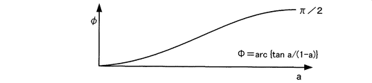
本実施の形態における受信電極が隣接する2つの送信電極の境界を通過する際に受信電極に誘起される電圧は次の通りである。2つの送信電極に印加される電圧をそれぞれsinωtおよびcosωtとし、cosωtの電圧が印加される電極の受信電極に対する影響度合いをa(0<a<1)とすると、sinωtの電圧が印加される電極の受信電極に対する影響度合いは(1−a)であり、両送信電極の影響を合成した電圧は式3のように表わされる。 The voltage induced in the receiving electrode when the receiving electrode in this embodiment passes through the boundary between two adjacent transmitting electrodes is as follows. If the voltages applied to the two transmission electrodes are sin ωt and cos ωt, respectively, and the influence degree of the electrode to which the voltage of cos ωt is applied to the reception electrode is a (0 <a <1), the electrode to which the voltage of sin ωt is applied The degree of influence on the receiving electrode is (1-a), and the voltage obtained by synthesizing the influences of the two transmitting electrodes is expressed by Equation 3.
《数3》
(1−a)sinωt+a cosωt={1−2a(1−a)}1/2sin(ωt+
φ) 式3
ただし、φは式4に示すものである。
《数4》
φ=arc tan{a/(1−a)} 式4
<< Equation 3 >>
(1-a) sin ωt + a cos ωt = {1-2a (1-a)} 1/2 sin (ωt +
φ) Equation 3
However, (phi) is shown in
<<
φ = arc tan {a / (1-a)}
cosωtの電圧が印加される電極の受信電極に対する影響度合いaは“0”〜“1”の範囲で変化するので、式4に示すように受信電極に誘起される電圧の位相φは、“0”〜“π/2”の範囲で変化する。図7に、影響度合いaと位相φとの関係を示す。
Since the influence degree a of the electrode to which the voltage of cos ωt is applied to the receiving electrode varies in the range of “0” to “1”, the phase φ of the voltage induced in the receiving electrode as shown in
また、式3に示すように、受信電極に誘起される電圧のレベルは“1”〜“(1/(21/2)”まで変化するが、“0”になることはない。これは、第1の実施の形態では隣接する送信電極間に印加される電圧が互いに逆相であったのに対して、本実施の形態ではπ/2であるためである。このように本実施の形態では受信電極に誘起する信号の振幅が極端に小さくなることなく保全出来る特長がある。このため受信電極に誘起する信号の位相の弁別をより確実に行なうことができる。 Further, as shown in Equation 3, the level of the voltage induced in the receiving electrode changes from “1” to “(1 / (2 1/2 )”, but does not become “0”. This is because, in the first embodiment, the voltages applied between adjacent transmission electrodes are opposite in phase to each other, whereas in this embodiment, the voltage is π / 2. The configuration has the advantage that the amplitude of the signal induced in the receiving electrode can be maintained without becoming extremely small, so that the phase of the signal induced in the receiving electrode can be more reliably discriminated.
図8には、第2の実施の形態における送信電極に印加する信号を発生する信号発生回路、送信電極、受信電極、受信電極に誘起された信号を処理する論理集積回路の内部構成を示している。以下の説明では、第1の実施の形態と同じ作用をするものに関しては同じ符号を付け、詳細な説明は省略する。 FIG. 8 shows an internal configuration of a signal generating circuit for generating a signal to be applied to the transmitting electrode, a transmitting electrode, a receiving electrode, and a logic integrated circuit for processing a signal induced in the receiving electrode in the second embodiment. Yes. In the following description, the same reference numerals are assigned to the same functions as those in the first embodiment, and detailed description thereof is omitted.
図8(a)にはハンマー104の先端部106部分の側面が、図8(b)には、信号発生回路、送信電極、受信電極、信号を処理する論理集積回路が示されている。なお、図8(b)には左上には送信電極、受信電極の関係が分かりやすいように電極を正面から見た図が示されている。図8(c)には送信電極に接続される配線の一部が拡大して示されている。
FIG. 8A shows a side surface of the
ハンマー104の先端部106には、第1の実施の形態と同様に矩形の4個の送信電極が備えられている。ただし、第2の実施の形態では、送信電極は4個とされており、送信電極801A、送信電極801B、送信電極801C、送信電極801Dが、この記載順にハンマー104の先端部106の移動方向に沿って上から所定の間隔をおいて絶縁固定されている。速度検出基板110には第1の実施の形態と同様に矩形の受信電極802が備えられている。ただし、第2の実施の形態では、受信電極は1個としている。
The
信号発生回路803は、正弦波発振器804、余弦波発振器805、平衡昇圧トランス806および平衡昇圧トランス807から構成されている。正弦波発振器804および余弦波発振器805からの出力は、それぞれ平衡昇圧トランス806および平衡昇圧トランス807によって2相の高圧交番信号とされる。従って、信号発生回路803からは位相がπ/2ずつ異なる4相の高圧の交番信号が発生される。なお、正弦波発振器および余弦波発振器として位相がπ/2異なる信号を発振する4相発振器(quadrature oscillator)が公知である。正弦波発振器804および余弦波発振器805が発生する交番信号は同じ電圧および同じ周期であり、また両発振器に接続された平衡昇圧トランス806および平衡昇圧トランス807の昇圧比も同じに設定されているため、4相の高圧の交番信号の電圧および周期は同一になっている。平衡昇圧トランス806からの出力される2相の交番信号のうちsin波は送信電極801Aに、−sin波は送信電極801Cに供給される。また平衡昇圧トランス807からの出力される2相の交番信号のうちcos波は送信電極801Bに、−cos波は送信電極801Dに供給される。すなわち、送信電極801Aにはsin波が、送信電極801Bにはcos波が、送信電極801Cには−sin波が、送信電極801Dには−cos波がそれぞれ印加される。従って隣接する送信電極間の位相差はπ/2(90度)になっている。
The
平衡昇圧トランス806から送信電極801Aおよび送信電極801Cに交番信号を供給する配線は、対として平行線あるいは撚り対線とされている。配線を通る信号は第1の実施の形態と同様に互いに逆相であるため、互いに相殺され配線からの不要輻射が低減される。同様に平衡昇圧トランス807から送信電極801Bおよび送信電極801Dに交番信号を供給する配線も、対として平行線あるいは撚り対線とされており、配線からの不要輻射が低減される。配線をシールド線とすればより不要輻射を低減することができる。なお、2つの平衡昇圧トランスから出力される信号は位相がπずつずれた4相であるため、これらの信号を加算すると互いに相殺される。従って、2つの平衡昇圧トランスから出力される4本の配線をまとめて平行線あるいは撚り線としても、互いに相殺されて不要輻射を低減することができる。
The wiring for supplying an alternating signal from the balanced step-up
図8(c)には、送信電極と平衡昇圧トランスを結ぶ配線のうち送信電極近傍部分が拡大して示されている。送信電極801Aには配線820Aが、送信電極801Bには配線820Bが、送信電極801Cには配線820Cが、送信電極801Dには配線820Dが、それぞれ接続されている。互いに逆相の信号が供給される配線820Aと配線820Cは近接した平行線とされており、同様に互いに逆相の信号が供給される配線820Bと配線820Dも近接した平行線とされている。さらに配線820Cと配線820Dとの間にはグランド電極821が設けられており、グランド電極821はグランドに接続されている。このような構成によって配線からの不要輻射を低減させている。
FIG. 8C shows an enlarged portion near the transmission electrode in the wiring connecting the transmission electrode and the balanced step-up transformer. A
受信電極802に誘起された交番信号は、論理集積回路808の電圧比較器809の正側入力端子に入力される。電圧比較器809の負側入力端子は第1の実施の形態の電圧比較器と同様に接地されており、電圧比較器809は交番信号を論理レベルに変換して位相パルス810とする。位相パルス810は位相弁別器811のゲート812に供給される。位相弁別器811は連続的な位相の変化を検出するもので、ゲート812、カウンタ813およびレジスタ814から構成されている。ゲート812には位相パルス810の他に、正弦波発振器804からの信号がレベルコンバータ209で論理レベルに変換された基準位相信号210およびマスタークロック発振器815からのマスタークロック816が与えられている。ゲート812は、位相パルス810の立ち上がりから基準位相信号210の立ち上がりまでの間にマスタークロック816を通過させて、ゲート出力817とする。ゲート出力817はカウンタ813に供給される。カウンタ813はゲート出力817を計数する。カウンタ813はゲート817が閉じた時にカウンタ813の計数値をレジスタ814に移す。レジスタ814はカウンタ813の計数値を位相出力としてマイクロプロセッサ212から読み出されるまで保持する。
The alternating signal induced at the
図9には、マスタークロック816、位相パルス810、基準位相信号210、ゲート出力817の関係が示されている。ゲート出力817は、位相パルス810の立ち上がりから基準位相信号210の立ち上がりまでの間にマスタークロック816を通過させることで生成され、位相パルス810の位相が基準位相信号210の位相よりも進むほどゲート出力817のパルス数が増える。ゲート出力817のパルス数を数えることにより受信電極802に誘起された交番信号の位相を検出することができる。
FIG. 9 shows the relationship among the
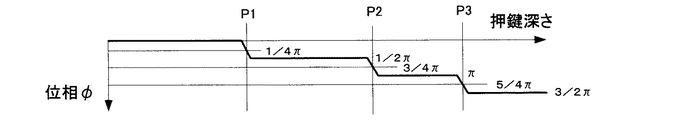
図10には、押鍵深さが変化したときに受信電極802に誘起される交番信号の位相を、sin波の位相を基準の位相として示している。押鍵深さP1は受信電極802が送信電極801Aと送信電極801Bの境界を通過する位置、押鍵深さP2は受信電極802が送信電極801Bと送信電極801Cの境界を通過する位置、押鍵深さP3は受信電極802が送信電極801Cと送信電極801Dの境界を通過する位置を示している。
FIG. 10 shows the phase of the alternating signal induced in the receiving
押鍵待機中は送信電極801Aに印加された信号sinωtが受信電極802に誘起する。このとき検出される位相は“0”となる。押鍵が開始され、押鍵深さがP1に達するまでは、検出される位相は“0”のままである。押鍵が進み、受信電極802が送信電極801Aと801Bの境界を通過するときに、送信電極801Aから誘起される信号sinωtは急速に減少し、送信電極801Bから誘起される信号cosωtが急速増加する。このとき検出される位相は”0“から”π/2“に急速に変化する。以降、同様に検出される位相は、押鍵深さがP2に達するまでは“π/2”、押鍵深さがP2を通過するときには“π/2”から“π”に変化し、さらに押鍵深さがP3に達するまでは“π”、押鍵深さがP3を通過するときには“π”から“3/2π”に変化する。
During key pressing standby, a signal sin ωt applied to the
マイクロプロセッサ212は第1の実施の形態における処理と同様に所定時間毎に処理を行い、位相出力に基づいて、位相がπ/2変化する時間間隔を測定することで押鍵の速度を検出する。すなわち、押鍵深さがP1から押鍵深さP2に変化する際の時間間隔から押鍵の初速度を求め、押鍵深さがP2からP3に変化する際の時間間隔から押鍵の最終速度を求めることができる。また、押鍵の初速度と最終速度の平均から押鍵の平均速度を求めることもできる。これらの押鍵速度は例えば次のように利用する。押鍵が初期位置から始められた場合には、押鍵の平均速度により発音を制御し、連打により押鍵が押鍵深さP1と押鍵深さP2の間から始められた場合には押鍵の最終速度によって発音を制御する。
The
図11には、マイクロプロセッサ212の処理内容が示されている。実際には複数の鍵の処理が時分割で行われるがここでは説明を簡略するために1つの鍵についてのみ解説する。この処理は充分に短い一定時間毎に繰り返し起動される。また処理に使う変数は図示しない処理により電源投入時に初期化されている。
FIG. 11 shows the processing contents of the
ステップS201では、レジスタ814に記憶されている位相出力値を読み込み、位相出力値の前回の処理からの変化を判別する。なお、前回の処理における位相値は後述するステップS231において記憶されている。位相が“π/4”を通過して増加した場合にはステップS202に進み、位相が“3π/4”を通過して増加した場合にはステップS204に進み、位相が“5π/4”を通過し増加した場合にはステップS210に進み、位相が“5π/4”を通過して減少した場合にはステップS219に進み、位相が“3π/4”を通過して減少した場合にはステップS221に進み、位相が“π/4”を通過して減少した場合にはステップS222に進み、その他の場合にはステップS227に進む。
In step S201, the phase output value stored in the
なお、図11では例えば「位相が“π/4”を通過して増加した場合」を「π/4
→」と表し、位相が“π/4”を通過して減少した場合」を「← π/4」と表記している。すなわち数値は通過する位相を示し、数値の右に「→」がある場合には増加したことを示し、数値の左に「←」がある場合には減少したことを示している。
In FIG. 11, for example, “when the phase increases through“ π / 4 ”” is changed to “π / 4”.
→ ”and“ when the phase decreases after passing through “π / 4” ”is expressed as“ ← π / 4 ”. In other words, the numerical value indicates a passing phase. When “→” is on the right side of the numerical value, it indicates that the phase has increased, and when “←” is on the left side of the numerical value, it indicates that it has decreased.
ステップS202では、押鍵速度カウンタの値をクリアしてステップS203に進む。ステップS203では、押鍵速度カウンタのカウントを開始し、ステップS231に進む。 In step S202, the value of the key pressing speed counter is cleared and the process proceeds to step S203. In step S203, the key pressing speed counter starts counting, and the process proceeds to step S231.
ステップS204では、押鍵速度カウンタのカウント中であるか判断し、カウント中である場合にはステップS205に進み、カウント中でない場合にはステップS206に進む。ステップS205では、押鍵速度カウンタのカウント値から押鍵の初速度を算出して記憶し、ステップS206に進む。ステップS206では、押鍵速度カウンタのカウンタ値をクリアしステップS207に進む。ステップS207では、押鍵速度カウンタのカウントを開始し、ステップS208に進む。ステップS208では、離鍵速度カウンタのカウント中であるか判断し、カウント中である場合にはステップS209に進み、カウント中でない場合にはステップS231に進む。ステップS209では、連打フラグに連打処理中であることを示す“1”を設定し、ステップS231に進む。 In step S204, it is determined whether the key pressing speed counter is being counted. If it is being counted, the process proceeds to step S205, and if it is not being counted, the process proceeds to step S206. In step S205, the initial key pressing speed is calculated from the count value of the key pressing speed counter and stored, and the process proceeds to step S206. In step S206, the count value of the key pressing speed counter is cleared, and the process proceeds to step S207. In step S207, the count of the key pressing speed counter is started, and the process proceeds to step S208. In step S208, it is determined whether the key release speed counter is being counted. If it is being counted, the process proceeds to step S209, and if it is not being counted, the process proceeds to step S231. In step S209, “1” indicating that the continuous hitting process is being performed is set in the consecutive hit flag, and the process proceeds to step S231.
ステップS210では、押鍵速度カウンタのカウント中であるか判断し、カウント中である場合にはステップS211に進み、カウント中でない場合にはステップS231に進む。ステップS211では、押鍵速度カウンタのカウントを停止してステップS212に進む。ステップS212では、押鍵速度カウンタのカウント値から押鍵の最終速度を算出して、ステップS213に進む。ステップS213では、連打フラグを参照して、連打処理中でないことを示す“0”である場合には、ステップS214に進み、連打処理中であることを示す“1”である場合には、ステップS215に進む。ステップS214では、記憶しておいた初速度と最終速度の平均を押鍵速度としステップS218に進む。ステップS215では、最終速度を押鍵速度としステップS216に進む。ステップS216では音源に離鍵速度情報を含むノートオフ指示を出力し、ステップS217に進む。なお、このときの離鍵速度情報の値は、離鍵速度の範囲の中央値とする。ステップS217では、連打フラグをクリアしステップS218に進む。ステップS218では、ステップS214あるいはステップS215で求めた押鍵速度情報を含むノートオン指示を音源に送出し、ステップS231に進む。 In step S210, it is determined whether the key pressing speed counter is being counted. If it is being counted, the process proceeds to step S211. If it is not being counted, the process proceeds to step S231. In step S211, the key pressing speed counter is stopped and the process proceeds to step S212. In step S212, the final key pressing speed is calculated from the count value of the key pressing speed counter, and the process proceeds to step S213. In step S213, referring to the continuous hitting flag, if it is “0” indicating that the continuous hitting process is not being performed, the process proceeds to step S214. If it is “1” indicating that the continuous hitting process is being executed, The process proceeds to S215. In step S214, the average of the stored initial speed and final speed is set as the key pressing speed, and the process proceeds to step S218. In step S215, the final speed is set as the key pressing speed, and the process proceeds to step S216. In step S216, a note-off instruction including key release speed information is output to the sound source, and the process proceeds to step S217. Note that the value of the key release speed information at this time is the median value of the key release speed range. In step S217, the consecutive hit flag is cleared and the process proceeds to step S218. In step S218, a note-on instruction including the key pressing speed information obtained in step S214 or step S215 is sent to the sound source, and the process proceeds to step S231.
ステップS219では、離鍵速度カウンタの値をクリアしてステップS220に進む。ステップS220では、離鍵速度カウンタのカウントを開始し、ステップS231に進む。 In step S219, the value of the key release speed counter is cleared and the process proceeds to step S220. In step S220, the counting of the key release speed counter is started, and the process proceeds to step S231.
ステップS221では、押鍵速度カウンタのカウントを停止してステップS231に進む。 In step S221, the count of the key pressing speed counter is stopped and the process proceeds to step S231.
ステップS222では、離鍵速度カウンタのカウント中であるか判断し、カウント中である場合にはステップS223に進み、カウント中でない場合にはステップS226に進む。ステップS223では、離鍵速度カウンタを停止しステップS224に進む。ステップS224では、離鍵速度カウンタのカウント値から離鍵速度を算出してステップS225に進む。ステップS225では、求めた離鍵速度情報を含むノートオフ指示を音源に送出し、ステップS226に進む。ステップS226では、連打フラグをクリアしステップS231に進む。 In step S222, it is determined whether the key release speed counter is being counted. If it is being counted, the process proceeds to step S223, and if it is not being counted, the process proceeds to step S226. In step S223, the key release speed counter is stopped and the process proceeds to step S224. In step S224, the key release speed is calculated from the count value of the key release speed counter, and the process proceeds to step S225. In step S225, a note-off instruction including the obtained key release speed information is sent to the sound source, and the process proceeds to step S226. In step S226, the consecutive hit flag is cleared and the process proceeds to step S231.
ステップS227では、押鍵速度カウンタのカウント中であるか判断し、カウント中である場合にはステップS228に進み、カウント中でない場合にはステップS229に進む。ステップS228では、押鍵速度カウンタの値をインクリメントしステップS229に進む。ステップS229では、離鍵速度カウンタのカウント中であるか判断し、カウント中である場合にはステップS230に進み、カウント中でない場合にはステップS231に進む。ステップS230では、離鍵速度カウンタの値をインクリメントしステップS231に進む。 In step S227, it is determined whether the key pressing speed counter is being counted. If it is being counted, the process proceeds to step S228, and if it is not being counted, the process proceeds to step S229. In step S228, the value of the key pressing speed counter is incremented and the process proceeds to step S229. In step S229, it is determined whether the key release speed counter is being counted. If it is being counted, the process proceeds to step S230, and if it is not being counted, the process proceeds to step S231. In step S230, the value of the key release speed counter is incremented and the process proceeds to step S231.
ステップS231では現在の位相出力値を記憶して処理を終了する。 In step S231, the current phase output value is stored and the process ends.
押鍵が開始されて押鍵深さがP1を通過したときには、ステップS202およびステップS203の処理によって押鍵速度カウントが開始される。続いて押鍵深さがP2を通過するまでの間は、ステップS228の処理によって押鍵速度カウンタの値がインクリメントされる。押鍵深さがP2を通過したときには、ステップS204〜S207の処理によって押鍵速度カウンタの値から押鍵の初速度が求められ、再び押鍵速度カウントが開始される。押鍵深さがP3を通過るまでの間は、ステップS228の処理によって押鍵速度カウンタの値がインクリメントされる。押鍵深さがP3を通過したときには、ステップS210〜S212の処理によって押鍵の最終速度が求められる。押鍵深さがP1→P2→P3の順に変化した場合には、ステップS214によって連打ではないと判断され、ステップS214によって押鍵の初速度と最終速度の平均値を押鍵速度としてステップS219によって音源にノートオンが指示される。 When the key pressing is started and the key pressing depth has passed P1, the key pressing speed count is started by the processing of step S202 and step S203. Subsequently, the value of the key pressing speed counter is incremented by the process of step S228 until the key pressing depth passes P2. When the key pressing depth has passed P2, the initial key pressing speed is obtained from the value of the key pressing speed counter by the processing of steps S204 to S207, and the key pressing speed counting is started again. Until the key pressing depth passes through P3, the value of the key pressing speed counter is incremented by the process of step S228. When the key pressing depth has passed P3, the final key pressing speed is obtained by the processing of steps S210 to S212. When the key pressing depth changes in the order of P1 → P2 → P3, it is determined in step S214 that it is not repeated, and in step S214, the average value of the initial key pressing speed and the final speed is set as the key pressing speed in step S219. A note-on is instructed to the sound source.
離鍵が開始されて押鍵深さがP3を通過したときには、ステップS219およびステップS220の処理によって離鍵速度カウントが開始される。続いて押鍵深さがP1を通過するまでの間は、ステップS230の処理によって離鍵速度カウンタの値がインクリメントされる。押鍵深さがP1を通過したときには、ステップS222〜S225の処理によって離鍵速度カウンタの値から離鍵速度が求められ、音源にノートオフが指示される。なお、離鍵操作は押鍵操作に比べて敏感な速度制御が行いにくいので、ノートオフ指示に含める離鍵速度情報は、押鍵深さがP3からP1までの経過時間に基づいて求めるようにしている。 When the key release is started and the key pressing depth has passed P3, the key release speed count is started by the processing of step S219 and step S220. Subsequently, the value of the key release speed counter is incremented by the process of step S230 until the key pressing depth passes P1. When the key pressing depth has passed P1, the key release speed is obtained from the value of the key release speed counter by the processing of steps S222 to S225, and note-off is instructed to the sound source. Since the key release operation is less sensitive than the key press operation, the key release speed information included in the note-off instruction is obtained based on the elapsed time from the key press depth P3 to P1. ing.
離鍵されて押鍵深さがP2を通過し、P1を通過する前に再び押鍵された場合には、押鍵深さがP2を通過した際に、ステップS208およびS209の処理によって連打フラグが設定され、押鍵深さがP3を通過した際に、ステップS213によって連打と判断されて、ステップS215の処理によって押鍵の最終速度が押鍵速度として採用される。そして、ステップS216で発音中の音に対するノートオフが音源に指示された後に、ステップS218で新たな押鍵に対するノートオンが音源に指示される。 When the key is released and the key pressing depth passes through P2, and the key is pressed again before passing through P1, when the key pressing depth passes through P2, the process of steps S208 and S209 causes the repeated hitting flag. Is set, and when the key pressing depth has passed P3, it is determined in step S213 that the keystroke is repeated, and the final key pressing speed is adopted as the key pressing speed by the processing in step S215. In step S216, the sound source is instructed to turn off the sound being sounded, and then in step S218, the sound source is instructed to turn on the note for a new key press.
なお、前述の処理では、マイクロプロセッサ212がレジスタ814に記憶された位相出力値を定期的に監視して、押鍵深さが所定のポイントを通過するのを検出するようにしたが、レジスタ814に記憶された値が所定の押鍵深さのポイントに対応する値を通過したときに、マイクロプロセッサ212に割り込みをかけて、マイクロプロセッサ212はこの割り込みに応じて処理を行うようにしてもよい。この場合には、レジスタ814に3個の値を記憶できるようにして、レジスタ814にカウンタ813の値を設定するのを止め、代わりにマイクロプロセッサ212から押鍵深さP1、押鍵深さP2および押鍵深さP3に対応する値を設定できるようにする。さらにカウンタ813とレジスタ814との間に比較器818を設けて、カウンタ813の値がレジスタ814に設定されているいずれかの値を超えたことを比較器818が検出した時に、マイクロプロセッサ212に割り込みをかけるようにする。このとき比較器818は、カウンタ813の値が増加方向に変化したのか減少方向に変化したのか、またカウンタ813の値がいずれの押鍵深さに対応する値を超えたのかを示す情報を保持し、マイクロプロセッサ212は、比較器818に保持されたこれらの情報を読み出して適宜処理を行う。このようにすればマイクロプロセッサ212は位相出力の値を定期的に監視する必要がなくなるため処理の負担が軽くなる。
In the above-described processing, the
本発明の第3の実施の形態について説明する。ピアノのような打弦楽器はハンマーが弦を打撃する瞬間、つまりハンマーの最終速度によって音量や音色が決定されるが、鍵の初速度や押鍵深さ、押鍵後の押圧(アフタータッチ)が発音に影響する場合がある。またシンセサイザーではこれらを有効に音色に反映させて変化させたいという要望がある。このような場合には、ハンマーの最終速度だけでなく、鍵の全ストロークの位置や速度を連続的に検出することが望まれる。また、第1の実施の形態、第2の実施の形態では、鍵の操作速度を測定する区間は送信電極の境界位置によって決められており、設計時に固定されている。しかし、演奏曲や演奏者の好みによって鍵の操作速度を測定する区間を自由に変更することが望まれる場合がある。 A third embodiment of the present invention will be described. For a stringed instrument such as a piano, the volume and tone are determined by the moment the hammer strikes the string, that is, the final speed of the hammer, but the initial speed and depth of the key, and the pressing after the key is pressed (aftertouch). May affect pronunciation. In addition, there is a demand for the synthesizer to effectively change these by reflecting them in the timbre. In such a case, it is desirable to continuously detect not only the final speed of the hammer but also the position and speed of the entire stroke of the key. In the first embodiment and the second embodiment, the section for measuring the key operation speed is determined by the boundary position of the transmission electrode, and is fixed at the time of design. However, there are cases where it is desired to freely change the section in which the key operation speed is measured depending on the performance music or the player's preference.
第3の形態では、鍵の全ストロークに渡って、その時点の鍵の押下深さを検出できるようにする。第1の実施の形態、第2の実施の形態では、送信電極間の境界はハンマーの移動方向に対して垂直方向に設けられている。図12(a)、(b)には、第3の実施の形態で用いられる送信電極の基本構造が示されている。送信電極1201がハンマー104の先端部106に設けられているのは、第1の実施の形態、第2の実施の形態と同じであるが、第3の実施の形態では、送信電極間の境界をハンマーの移動方向に対して傾斜させ、楔形の銅箔で形成された送信電極1201A、1201Bをハンマー104の先端部106に設ける。すなわち、一方の送信電極の幅をハンマー104の移動方向に対して徐々に増大し、その送信電極に隣接する他方の送信電極の幅は逆にハンマー104の移動方向に対して徐々に減少するようにする。
In the third embodiment, the key pressing depth at that time can be detected over the entire stroke of the key. In the first embodiment and the second embodiment, the boundary between the transmission electrodes is provided in a direction perpendicular to the moving direction of the hammer. 12A and 12B show the basic structure of the transmission electrode used in the third embodiment. The
前記の構成において、送信電極121Aに正弦波の交番電圧を、901Bに余弦波の交番電圧をそれぞれ印加して、受信電極802が送信電極の近傍を相対的に移動すると、受信電極802に誘起する信号の位相は、連続的にπ/2(90度)変化する。
In the above configuration, when a sine wave alternating voltage is applied to the transmission electrode 121A and a cosine wave alternating voltage is applied to the transmission electrode 901B and the
図13には、第3の形態において送信電極の数を4とし、送信電極の数が2の場合と比べて位相の変化量を3倍に拡大した場合の送信電極に印加する信号を発生する信号発生回路、送信電極、受信電極が示されている。以下の説明では、今まで説明した第1の実施の形態あるいは第2の実施の形態と同じ作用をするものに関しては詳細な説明を省略する。図13(a)には、ハンマーの先端部106と送信電極1301および受信電極802を側面から見た図が、図13(b)には、送信電極1301および受信電極802を正面から見た図が示されている。受信電極802は、第1の実施の形態、第2の実施の形態と同様に、鍵盤基部の速度検出基板に水平に固定されている。送信電極1301は、送信電極1301A、送信電極1301B、送信電極1301Cおよび送信電極1301Dから構成されており、隣接する送信電極間の境界はハンマーの移動方向に対して傾斜している。送信電極1301の最上部では送信電極1301Aのみが存在し、下がるに連れて送信電極1301Aの幅が徐々に減少し逆に送信電極1301Bの幅が徐々に増大する。送信電極1301Aが途切れた位置から下では送信電極1301Bの幅が徐々に減少し、逆に送信電極1301Cの幅が徐々に増大する。送信電極1301Bが途切れた位置から下では送信電極1301Cの幅が徐々に減少し、逆に送信電極1301Dの幅が徐々に増大する。図12に示した電極は楔形であったが、図13に示す送信電極1301Aおよび送信電極1301Dは楔形、送信電極1301Bおよび送信電極1301Cは台形となっている。
In FIG. 13, in the third embodiment, the number of transmission electrodes is four, and a signal applied to the transmission electrodes is generated when the amount of phase change is increased three times compared to the case where the number of transmission electrodes is two. A signal generation circuit, a transmission electrode, and a reception electrode are shown. In the following description, detailed description is omitted for those having the same functions as those of the first embodiment or the second embodiment described so far. FIG. 13A shows the
ハンマーの先端部106の上下移動に伴って、受信電極802は送信電極1301A〜送信電極1301Dのそれぞれの発する電界の影響を受ける。信号発生回路は、第2の実施の形態に示したものと同様に、4相の交番信号を発生する。そして送信電極1301Aにはsin波が、送信電極1301Bにはcos波が、送信電極1301Cには−sin波が、送信電極1301Dには−cos波がそれぞれ印加される。
As the
図14には、各送信電極に印加される信号、押鍵深さが変化したときに受信電極802に誘起される交番信号の位相を、sin波の位相を基準の位相として示している。図14の最下段には、横軸に押鍵の深さ、縦軸に受信電極802に誘起される交番信号の位相が示されている。
FIG. 14 shows the phase of an alternating signal induced in the receiving
図14に示すa(0<a<1)は、受信電極802が送信電極1301Aに対向する位置にあるときの、受信電極802に対する送信電極1301Aの影響度合いを示している。このとき、受信電極802に対する送信電極1301Bの影響度合いは“1−a”と表わされる。受信電極802が図の右側に移動するのに連れて、受信電極802に対向する送信電極1301Aの幅は減少し、送信電極1301Bの幅が増大する。このとき、受信電極802に誘起される電圧および位相は、前述の式3、式4に従って変化する。図14の最下段には位相の変化の様子が示されている。
14 (0 <a <1) illustrated in FIG. 14 indicates the degree of influence of the
受信電極802が押鍵開始点P0の位置にあるときには、受信電極802は送信電極1301Aだけの影響を受けてsinωtの電圧が誘起される。受信電極802が相対的に図の右側に移動するのに連れて、受信電極802に対向する送信電極1301Aの幅は減少し、逆に送信電極1301Bの幅が増大する。この結果、sinωtの影響が減少し、逆にcosωtの影響が増大し、受信電極802に誘起される位相は徐々に進む。受信電極802が送信電極1301Aが途切れる位置まで来たときには、受信電極802にはcosωtの電圧が誘起され、基準位相sinωtに比べて位相が“π/2”進む。受信電極3がさらに右側に移動すると、今度は受信電極802に対向する送信電極1301Bの幅が減少し、送信電極1301Cの幅が増大する。これに伴い、位相はsinωtに比べて“π/2”から“π”まで変化する。同様に受信電極802が右端に到達するまでの間に位相が“π”から“3π/2”まで変化する。
When the
第3の実施の形態では、予め任意に設定された押鍵深さP1、押鍵深さP2および押鍵深さP3を通過する時間間隔を計測して、第2の実施の形態と同様に鍵の操作速度を求める。押鍵深さP1、押鍵深さP2および押鍵深さP3は、演奏者の好みによって変更することができる。また、第3の実施の形態では、押鍵の深さを連続的に検出して、発音する音色の修飾に利用する。 In the third embodiment, the time interval passing through the key depression depth P1, the key depression depth P2, and the key depression depth P3 which are arbitrarily set in advance is measured, and the same as in the second embodiment. Find the key operation speed. The key pressing depth P1, the key pressing depth P2, and the key pressing depth P3 can be changed according to the player's preference. In the third embodiment, the key depression depth is continuously detected and used for modification of the tone to be generated.
なお、図7では受信電極に対する2つの送信電極の影響度合いと検出される位相の関係は曲線状になっているのに対して図14では両者の関係が直線状になっているが、送信電極の形状を補正したり、検出した位相を予め計算したテーブルを参照して補正したりすることで、両者の関係を直線状にすることができる。また、受信電極に誘起された信号を処理して位相弁別を行なう回路は、図8に示したものと同様のものを用いることができるので説明を省略する。 In FIG. 7, the relationship between the degree of influence of the two transmission electrodes on the reception electrode and the detected phase is curved, whereas in FIG. 14, the relationship between the two is linear. By correcting the shape or correcting the detected phase with reference to a previously calculated table, the relationship between the two can be made linear. Further, a circuit for processing the signal induced in the receiving electrode and performing phase discrimination can be the same as that shown in FIG.
図15には、マイクロプロセッサ212の処理内容が示されている。実際には複数の鍵の処理が時分割で行われるが、ここでは説明を簡略するために1つの鍵についてのみ解説する。この処理は充分に短い一定時間毎に繰り返し起動される。また処理に使う変数は図示しない処理により電源投入時に初期化されている。
FIG. 15 shows the processing contents of the
図15に示す処理は、図11に示した第2の実施の形態における処理とほぼ同じものであるので、相違点のみを説明する。 The process shown in FIG. 15 is almost the same as the process in the second embodiment shown in FIG. 11, so only the differences will be described.
ステップS301では、レジスタ814に記憶されている位相出力値を読み込み、位相出力値の前回の処理からの変化を判別する。このとき図11のステップS201では、現在の位相値を固定の位相値と比較するようにしたが、図15に示す処理では、現在の位相値を任意に設定された位相値と比較する点が異なる。比較対象の位相値は、演奏者が指定する押鍵深さP1、押鍵深さP2および押鍵深さP3に応じて図示しない別の処理によって予め設定されている。図15では、比較対象の位相値を“P1”、“P2”および“P3”として表記している。
In step S301, the phase output value stored in the
また、図15に示す処理では図11に示す処理に比べて、ステップS332が処理の末尾に追加されている点が異なる。ステップS332では、図14の下部に示した押鍵深さと位相値との関係に基づいて、現在の位相値を押鍵深さに換算して押鍵深さを示す情報を音源に送出する。音源では押鍵深さを示す情報に基づいて発音中の音色を修飾する。 Also, the process shown in FIG. 15 differs from the process shown in FIG. 11 in that step S332 is added to the end of the process. In step S332, based on the relationship between the key pressing depth and the phase value shown in the lower part of FIG. 14, the current phase value is converted into the key pressing depth, and information indicating the key pressing depth is sent to the sound source. The tone generator modifies the timbre during sound generation based on the information indicating the key depression depth.
本実施の形態では、マイクロプロセッサ212は押鍵の全ストロークにわたって検出された位相値を連続的に監視しているので、鍵の操作速度だけでなく押鍵の深さ、特に発音開始後の押鍵深さであるP3〜P4の最深部(アフタータッチ)の位置を連続的に音源に送出することができる。
In the present embodiment, since the
本発明の第4の実施の形態について説明する。第1の実施の形態、第2の実施の形態で示したものでは、矩形の複数の送信電極をハンマーの移動方向に沿って所定の間隔を置いて配置しており、送信電極間の境界の位置で受信電極に誘起する信号の位相が急激に変化するようになっている。第1及び第2の実施形態の方式では、局所空間精度を向上させて固定された境界間の通過時間から鍵の操作速度を正確に計算している。 A fourth embodiment of the present invention will be described. In the first and second embodiments, a plurality of rectangular transmission electrodes are arranged at predetermined intervals along the movement direction of the hammer, and the boundary between the transmission electrodes is The phase of the signal induced in the receiving electrode at the position changes abruptly. In the systems of the first and second embodiments, the key operation speed is accurately calculated from the passage time between fixed boundaries with improved local space accuracy.
これに対して、第3の実施の形態で示したものでは、送信電極の形状を楔形あるいは台形として、送信電極間の境界がハンマーの移動方向に対して傾斜するように送信電極を配置しており、受信電極に誘起する信号の位相が押鍵の全ストロークに渡って連続的に変化するようになっている。第3の実施形態の方式では、局所分解能を多少、犠牲にして押鍵の深さを連続的に検出できるようにしている。 In contrast, in the third embodiment, the shape of the transmission electrode is a wedge or trapezoid, and the transmission electrode is arranged so that the boundary between the transmission electrodes is inclined with respect to the movement direction of the hammer. Thus, the phase of the signal induced in the receiving electrode is continuously changed over the entire stroke of the key depression. In the system of the third embodiment, the key depression depth can be detected continuously at the expense of some local resolution.
第4の実施の形態では、上述の2つの方式の特長を同時に実現する。第4の実施の形態では、楔形、台形、矩形の送信電極を適宜組み合わせて、送信電極間の境界をハンマーの移動方向に対して傾斜させたり、垂直方向にしたりする。 In the fourth embodiment, the features of the two methods described above are realized simultaneously. In the fourth embodiment, wedge-shaped, trapezoidal, and rectangular transmission electrodes are appropriately combined, and the boundary between the transmission electrodes is inclined with respect to the moving direction of the hammer or is set in the vertical direction.
図16には、第4の実施の形態における送信電極、受信電極および信号発生回路が示されている。送信電極1601は、楔形の送信電極1601A、台形の送信電極1601B、楔形の送信電極1601C、送信電極1601D、送信電極1601E、送信電極1601F、送信電極1601Gから構成されている。送信電極1601Aと送信電極1601Bの間の境界、送信電極1601Bと送信電極1601Cの境界、送信電極1601Dと送信電極1601Eの境界、及び送信電極1601Fと送信電極1601Gの境界は、ハンマーの先端部106の移動方向に対して傾斜している。また、送信電極1601Cと送信電極1601Dの間の境界および送信電極1601と送信電極1601Gの境界は、ハンマーの先端部106移動方向に対して垂直方向になっている。送信電極1601の最上部では送信電極1601Aのみが存在し、下に下がるに連れて送信電極1601Aの幅が徐々に減少し、逆に送信電極1601Bの幅が徐々に増大する。送信電極1601Aが途切れた位置から下では送信電極1601Bの幅が徐々に減少し、逆に送信電極1601Cの幅が徐々に増大する。以下同様に、送信電極の幅が連続的に変化して行く。送信電極1601Cの下には送信電極1601Dが、送信電極1601Eの下には送信電極1601Fが順に水平に所定の間隙を置いて配置されている。
FIG. 16 shows a transmission electrode, a reception electrode, and a signal generation circuit in the fourth embodiment. The
図17には、各送信電極に印加する信号、押鍵深さが変化したときに受信電極802に誘起される交番信号の位相を、sin波の位相を基準の位相として示している。送信電極1601Aにはsinωtが、送信電極1601Bにはcosωtが、送信電極1601Cには−sinωtが、送信電極1601Dには−cosωtが、送信電極1601Eにはsinωtが、送信電極1601Fにはcosωtが、送信電極1601Gには−sinωtが、それぞれ印加されている。送信電極1601Cと送信電極1601Dとの間の境界を押鍵深さP2、送信電極1601Eと送信電極1601Gとの間の境界を押鍵深さP3としている。押鍵開始位置P0から押鍵深さP2までの間では誘起される信号の位相が連続的に変化し、押鍵深さP2の前後では誘起される信号の位相が急激に変化し、押鍵深さP2から押鍵深さP3までの間では誘起される信号の位相が連続的に変化し、押鍵深さP3の前後では誘起される信号の位相が急激に変化し、押鍵深さP3よりも深い押鍵深さでは誘起される信号の位相が連続的に変化している。
FIG. 17 shows the phase of the alternating signal induced in the receiving
正確な押鍵速度は、位相が急速に遷移する押鍵深さP2と押鍵深さP3との間の時間間隔で測定する。処理の詳細やフロー図は前述の実施の形態に準ずるので省略する。 The exact key pressing speed is measured at a time interval between the key pressing depth P2 and the key pressing depth P3 at which the phase rapidly changes. The details of the processing and the flow diagram are the same as those in the above-described embodiment, and will be omitted.
なお、前記実施の形態では、複数の送信電極に印加する交番信号を2相あるいは4相としたが、送信電極間の位相差を2π/3とした3相としてもよい。3相の交番信号も加算すると互いに相殺されるため不要輻射を低減することができる。また、前記の実施の形態では、送信電極を押鍵に伴って動く部材であるハンマーに設け、受信電極を鍵盤機構の基部に設けるようにしたが、両電極の対抗する面積が押鍵に伴って変化すれば前述の構成とは別の構成としてもよい。例えば、押鍵に伴って動く部材としてはハンマーの他に、鍵そのものであってもよい。あるいは図18に示すように、送信電極と受信電極を入れ替えて、送信電極1801を鍵盤基部108に設け、受信電極1802を鍵101の押鍵に伴って動く部材1803に設けるようにしてもよい。信号発生回路201および論理集積回路112を搭載した速度検出基盤は鍵盤基部108に設ける。ここで送信電極1801は、送信電極1801A、送信電極1801B、送信電極1801Cおよび送信電極1801Dから構成されている。また、受信電極1802は送信電極に対向するように押鍵に伴って動く部材1803の先端部に配置されている。なお、受信電極1802の押鍵に伴う移動経路は曲線になるため、送信電極1801と受信電極1802と間の最短距離が押鍵深さによらず一定になるように送信電極1801を受信電極1802の移動曲線に沿って湾曲させるのが好ましい。図18の構成によれば、鍵盤基部に設けられた信号発生回路から送信電極までの距離を短くすることができるため、配線からの不要輻射を低減させることができる。また、送信電極と受信電極の押鍵に伴って動く部材の移動方向の長さは、送信電極よりも受信電極の方が小さくされているため、図18に示すように受信電極を押鍵に伴って動く部材に設けるようにした場合には、鍵盤機構を小型化することができる。なお、図18には楔形あるいは台形の送信電極を示したが、送信電極の形状を図1や図8示すような矩形とすることもできる。この場合には、送信電極を各鍵に個々に独立して設けるのではなく、送信電極を鍵の配列方向に複数の鍵に跨る長さとして複数の鍵に共通する送信電極としてもよい。この場合、送信電極を鍵の配列方向に長く伸ばすことにより送信電極からの不要輻射が増加する要因となりえるが複数の送信電極に印加する交番信号は加算したときに相殺される位相差とされているため、送信電極からの不要輻射は問題にならない値となる。なお、受信電極が鍵側に設けられ受信電極から速度検出基板への配線が伸びるため、この配線にグランドラインで挟まれたシールドを施してこの配線に周辺の空間からの妨害電波が乗るのを防ぐようにすることが好ましい。
In the above embodiment, the alternating signal applied to the plurality of transmission electrodes is two-phase or four-phase, but it may be three-phase with the phase difference between the transmission electrodes being 2π / 3. If three-phase alternating signals are also added, they cancel each other out, so that unnecessary radiation can be reduced. In the above-described embodiment, the transmission electrode is provided on the hammer that is a member that moves with key depression, and the reception electrode is provided at the base of the keyboard mechanism. However, the opposing area of both electrodes is associated with key depression. However, the configuration may be different from the above configuration. For example, the member that moves along with the key press may be a key in addition to a hammer. Alternatively, as shown in FIG. 18, the transmission electrode and the reception electrode may be interchanged so that the
101 鍵
104 ハンマー
108 鍵盤基部
109 送信電極
110 速度検出基盤
111 受信電極
112 論理集積回路
201 信号発生回路
202 正弦波発振器
203 平衡昇圧トランス
204 配線
208 位相比較器
212 マイクロプロセッサ
801 送信電極
802 受信電極
803 信号発生回路
804 正弦波発振器
805 余弦波発振器
806 平衡昇圧トランス
807 平衡昇圧トランス
808 論理集積回路
811 位相弁別器
1201 送信電極
1301 送信電極
1601 送信電極
1801 送信電極
1802 受信電極
DESCRIPTION OF
Claims (11)
前記受信電極と対向して配置された2個以上の送信電極と、
対応する鍵の押鍵操作によって前記受信電極または送信電極の何れかが移動して前記受信電極と送信電極間の静電容量が変化する鍵盤機構と、
複数の鍵に共通して設けられ、周期が同一でかつ位相が互いに異なる複数の交番信号を発生し、発生した各交番信号を前記各送信電極にそれぞれ供給するとともに、該交番信号と同じ周期の基準位相信号を発生する信号発生回路と、
複数の鍵に共通に設けられ、該複数の鍵の各鍵に設けられた前記受信電極に誘起された交番信号および前記基準位相信号が供給され、前記基準位相信号を用いて各鍵の受信電極に誘起された交番信号の位相を弁別することで該鍵の押圧深さを求め、鍵が少なくとも2個の押圧深さを通過する際の時間間隔を計測することで鍵の操作速度を求める信号処理回路と、
を備える電子楽器の鍵操作速度検出装置。 One or a plurality of receiving electrodes corresponding to each key of the plurality of keys;
Two or more transmitter electrodes disposed opposite the receiver electrodes;
A keyboard mechanism in which either the reception electrode or the transmission electrode is moved by pressing a corresponding key to change the capacitance between the reception electrode and the transmission electrode;
A plurality of alternating signals that are provided in common to a plurality of keys and have the same period and different phases are supplied to each of the transmission electrodes, and each of the generated alternating signals has the same period as the alternating signal. A signal generation circuit for generating a reference phase signal;
The alternating signal and the reference phase signal that are provided in common to a plurality of keys and are induced in the reception electrodes provided in the keys of the plurality of keys are supplied, and the reception electrodes of the keys are used by using the reference phase signal. A signal for determining the key pressing speed by determining the key pressing depth by discriminating the phase of the alternating signal induced in the key, and measuring the time interval when the key passes at least two pressing depths. A processing circuit;
An electronic musical instrument key operation speed detecting device.
前記受信電極と前記送信電極との間には所定の間隙が設けられている電子楽器の鍵操作速度検出装置。 The key operation speed detection device for an electronic musical instrument according to claim 1,
An electronic musical instrument key operation speed detection device in which a predetermined gap is provided between the reception electrode and the transmission electrode.
前記信号発生回路は、前記受信電極に誘起される交番信号の電圧が前記信号処理回路で処理可能なレベルになるように前記基準位相信号よりも高電圧の交番信号を前記送信電極に供給する電子楽器の鍵操作速度検出装置。 The key operation speed detection device for an electronic musical instrument according to claim 2,
The signal generating circuit is an electron that supplies an alternating signal having a voltage higher than that of the reference phase signal to the transmitting electrode so that the voltage of the alternating signal induced in the receiving electrode is at a level that can be processed by the signal processing circuit. Instrument key operation speed detection device.
前記送信電極、前記受信電極のいずれか、あるいは双方が絶縁膜で覆われている電子楽器の鍵操作速度検出装置。 The key operation speed detection device for an electronic musical instrument according to claim 3,
A key operation speed detecting device for an electronic musical instrument in which either or both of the transmission electrode and the reception electrode are covered with an insulating film.
前記信号発生回路で発生する複数の交番信号を前記送信電極に供給する配線は、位相が互いにπ異なる交番信号を対として平行線あるいは撚り対線で前記送信電極に供給する電子楽器の鍵操作速度検出装置。 The key operation speed detection device for an electronic musical instrument according to claim 3,
The wiring for supplying a plurality of alternating signals generated by the signal generating circuit to the transmitting electrode is a key operation speed of an electronic musical instrument for supplying alternating signals having a phase different from each other by a pair of parallel lines or twisted pairs to the transmitting electrode. Detection device.
前記信号発生回路で発生する複数の交番信号の位相は該複数の交番信号を加算したときに交番信号が相殺される位相に設定されているとともに、該複数の交番信号を前記送信電極に供給する配線は平行線、撚り対線、またはこれらの線をシールドで覆ったシールド線とすることで該配線からの不要輻射を相殺する電子楽器の鍵操作速度検出装置。 The key operation speed detection device for an electronic musical instrument according to claim 3,
The phases of the plurality of alternating signals generated in the signal generating circuit are set to phases that cancel the alternating signals when the plurality of alternating signals are added, and the plurality of alternating signals are supplied to the transmission electrode. A device for detecting a key operation speed of an electronic musical instrument, wherein the wiring is a parallel wire, a twisted pair wire, or a shielded wire in which these wires are covered with a shield to cancel unnecessary radiation from the wire.
前記受信電極は、各鍵に対応して複数設けられており、
前記送信電極は、2個設けられており、
前記信号発生回路は、2個の送信電極に位相が互いにπ異なる2個の交番信号をそれぞれ供給するものであり、
前記信号処理回路は、各鍵の少なくとも2つの受信電極からの交番信号が位相反転する時間間隔から鍵の操作速度を求める電子楽器の鍵操作速度検出装置。 The key operation speed detection device for an electronic musical instrument according to claim 1,
A plurality of the receiving electrodes are provided corresponding to each key,
Two transmission electrodes are provided,
The signal generation circuit supplies two alternating signals having phases different from each other by π to the two transmission electrodes,
The signal processing circuit is a key operation speed detection device for an electronic musical instrument that calculates a key operation speed from a time interval at which alternating signals from at least two receiving electrodes of each key are phase-inverted.
前記受信電極は、各鍵に対応して1個設けられており、
前記送信電極は、2個以上設けられており、
前記信号処理回路は、各鍵の受信電極からの前記交番信号の位相が少なくとも2つの所定の位相と同一になった際の時間間隔から鍵の操作速度を求める電子楽器の鍵操作速度検出装置。 The key operation speed detection device for an electronic musical instrument according to claim 1,
One receiving electrode is provided corresponding to each key,
Two or more transmission electrodes are provided,
An apparatus for detecting a key operation speed of an electronic musical instrument, wherein the signal processing circuit obtains a key operation speed from a time interval when the phase of the alternating signal from the reception electrode of each key becomes equal to at least two predetermined phases.
前記鍵あるいは該鍵に連動する部材に前記送信電極が設けられているとともに、前記鍵盤機構の基部に前記受信電極および前記信号処理回路が設けられている電子楽器の鍵操作速度検出装置。 The key operation speed detection device for an electronic musical instrument according to claim 1,
A key operation speed detecting device for an electronic musical instrument, wherein the transmitting electrode is provided on the key or a member interlocking with the key, and the receiving electrode and the signal processing circuit are provided at a base portion of the keyboard mechanism.
前記鍵あるいは該鍵に連動する部材に前記受信電極が設けられているとともに、前記鍵盤機構の基部に前記送信電極および前記信号発生回路が設けられている電子楽器の鍵操作速度検出装置。 The key operation speed detection device for an electronic musical instrument according to claim 1,
A key operation speed detecting device for an electronic musical instrument, wherein the receiving electrode is provided on the key or a member interlocking with the key, and the transmitting electrode and the signal generating circuit are provided at a base portion of the keyboard mechanism.
前記受信電極に誘起された交番信号を前記信号処理回路に供給する配線にグランドラインで挟まれたシールドが施されている電子楽器の鍵操作速度検出装置。 The key operation speed detection device for an electronic musical instrument according to claim 10,
A key operation speed detecting device for an electronic musical instrument, wherein a shield sandwiched between ground lines is provided on a wiring for supplying an alternating signal induced in the receiving electrode to the signal processing circuit.
Priority Applications (5)
| Application Number | Priority Date | Filing Date | Title |
|---|---|---|---|
| JP2009279596A JP2011123191A (en) | 2009-12-09 | 2009-12-09 | Key operation speed detection device of electronic musical instrument |
| US12/957,055 US8134065B2 (en) | 2009-12-09 | 2010-11-30 | Key speed sensor of electronic instrument |
| AT10193626T ATE544148T1 (en) | 2009-12-09 | 2010-12-03 | KEY SPEED SENSOR FOR ELECTRONIC MUSICAL INSTRUMENTS |
| EP10193626A EP2352141B1 (en) | 2009-12-09 | 2010-12-03 | Key speed sensor of electronic musical instrument |
| CN2010105866572A CN102163425A (en) | 2009-12-09 | 2010-12-09 | Key speed sensor of electronic instrument |
Applications Claiming Priority (1)
| Application Number | Priority Date | Filing Date | Title |
|---|---|---|---|
| JP2009279596A JP2011123191A (en) | 2009-12-09 | 2009-12-09 | Key operation speed detection device of electronic musical instrument |
Publications (2)
| Publication Number | Publication Date |
|---|---|
| JP2011123191A true JP2011123191A (en) | 2011-06-23 |
| JP2011123191A5 JP2011123191A5 (en) | 2012-12-06 |
Family
ID=43706327
Family Applications (1)
| Application Number | Title | Priority Date | Filing Date |
|---|---|---|---|
| JP2009279596A Withdrawn JP2011123191A (en) | 2009-12-09 | 2009-12-09 | Key operation speed detection device of electronic musical instrument |
Country Status (5)
| Country | Link |
|---|---|
| US (1) | US8134065B2 (en) |
| EP (1) | EP2352141B1 (en) |
| JP (1) | JP2011123191A (en) |
| CN (1) | CN102163425A (en) |
| AT (1) | ATE544148T1 (en) |
Cited By (1)
| Publication number | Priority date | Publication date | Assignee | Title |
|---|---|---|---|---|
| JP2015045829A (en) * | 2013-08-29 | 2015-03-12 | カシオ計算機株式会社 | Touch detection device, touch detection method and program |
Families Citing this family (8)
| Publication number | Priority date | Publication date | Assignee | Title |
|---|---|---|---|---|
| US8319089B2 (en) * | 2010-09-07 | 2012-11-27 | William Henry Morong | Oscillatory, magnetically activated position sensor |
| JP5976362B2 (en) | 2012-03-29 | 2016-08-23 | 株式会社河合楽器製作所 | Electronic keyboard instrument |
| WO2015188388A1 (en) * | 2014-06-13 | 2015-12-17 | 浙江大学 | Proteinase |
| JP6299621B2 (en) | 2015-02-04 | 2018-03-28 | ヤマハ株式会社 | Keyboard instrument |
| JP6485082B2 (en) | 2015-02-04 | 2019-03-20 | ヤマハ株式会社 | Keyboard instrument |
| JP6070735B2 (en) * | 2015-02-04 | 2017-02-01 | ヤマハ株式会社 | Keyboard instrument |
| JP6645128B2 (en) * | 2015-11-04 | 2020-02-12 | ヤマハ株式会社 | Keyboard instrument and method for acquiring correction information in the keyboard instrument |
| WO2018168952A1 (en) * | 2017-03-15 | 2018-09-20 | ヤマハ株式会社 | Signal supply device, keyboard device, and program |
Family Cites Families (19)
| Publication number | Priority date | Publication date | Assignee | Title |
|---|---|---|---|---|
| US2329544A (en) * | 1941-07-16 | 1943-09-14 | Central Commercial Co | Condenser |
| US2623996A (en) * | 1948-06-10 | 1952-12-30 | Gen Precision Lab Inc | Capacity motion responsive device |
| US2809547A (en) * | 1955-01-28 | 1957-10-15 | Ca Nat Research Council | Intensity control device for electrical musical instrument |
| US2878708A (en) * | 1956-10-03 | 1959-03-24 | Hammond Organ Co | Capacitative switching apparatus |
| JPS5542759B2 (en) * | 1973-11-02 | 1980-11-01 | ||
| US4163222A (en) * | 1976-02-27 | 1979-07-31 | Amkey, Incorporated | Synchronous phase detected keyboard |
| SE411392B (en) | 1977-12-09 | 1979-12-17 | Inst Mikrovagsteknik Vid Tekni | METHOD DEVICE FOR CAPACITIVE DETERMINATION OF THE INSIDE DOCTOR AT TWO RELATIVELY ONE MOVING PARTS |
| US4420724A (en) * | 1982-05-17 | 1983-12-13 | Bell Telephone Laboratories, Incorporated | FET Amplifier with wide dynamic range |
| US4558623A (en) * | 1984-02-07 | 1985-12-17 | Kimball International, Inc. | Velocity and aftertouch sensitive keyboard |
| US4628786A (en) * | 1984-02-07 | 1986-12-16 | Kimball International, Inc. | Velocity responsive musical instrument keyboard |
| JPS62235504A (en) | 1986-04-04 | 1987-10-15 | Mitsutoyo Corp | Capacity-type position measuring transducer |
| JP2552300B2 (en) | 1987-07-06 | 1996-11-06 | 新王子製紙株式会社 | Thermal recording paper |
| JPH0467882A (en) | 1990-07-06 | 1992-03-03 | Yamamoto Press Kogyosho:Yugen | Kitchen knife for frozen food |
| JPH0467883A (en) | 1990-07-06 | 1992-03-03 | Pegasus Sewing Mach Mfg Co Ltd | Hem stitching pattern forming device for hem stitching sewing machine provided with thread supply device |
| JP3465312B2 (en) | 1993-09-16 | 2003-11-10 | ヤマハ株式会社 | Controller for electronic musical instruments |
| JP3914589B2 (en) | 1995-11-20 | 2007-05-16 | 東プレ株式会社 | Operating device |
| JPH1026983A (en) | 1996-07-11 | 1998-01-27 | Matsushita Electric Ind Co Ltd | Keyboard device for electronic musical instrument |
| JPH1167883A (en) | 1997-08-14 | 1999-03-09 | Sony Corp | Electrostatic chuck |
| JP5053175B2 (en) | 2008-05-20 | 2012-10-17 | 新日本製鐵株式会社 | Metal forging method and metal forging device |
-
2009
- 2009-12-09 JP JP2009279596A patent/JP2011123191A/en not_active Withdrawn
-
2010
- 2010-11-30 US US12/957,055 patent/US8134065B2/en not_active Expired - Fee Related
- 2010-12-03 AT AT10193626T patent/ATE544148T1/en active
- 2010-12-03 EP EP10193626A patent/EP2352141B1/en active Active
- 2010-12-09 CN CN2010105866572A patent/CN102163425A/en not_active Withdrawn
Cited By (1)
| Publication number | Priority date | Publication date | Assignee | Title |
|---|---|---|---|---|
| JP2015045829A (en) * | 2013-08-29 | 2015-03-12 | カシオ計算機株式会社 | Touch detection device, touch detection method and program |
Also Published As
| Publication number | Publication date |
|---|---|
| US8134065B2 (en) | 2012-03-13 |
| EP2352141A1 (en) | 2011-08-03 |
| EP2352141B1 (en) | 2012-02-01 |
| US20110132182A1 (en) | 2011-06-09 |
| ATE544148T1 (en) | 2012-02-15 |
| CN102163425A (en) | 2011-08-24 |
Similar Documents
| Publication | Publication Date | Title |
|---|---|---|
| JP2011123191A (en) | Key operation speed detection device of electronic musical instrument | |
| JP7009648B2 (en) | Keyboard sensor system and method | |
| JP6602566B2 (en) | Absolute encoder scale with plates repeatedly arranged against changing notches | |
| JP2011123191A5 (en) | ||
| JP2007240479A (en) | Capacitance type position detector | |
| CN112567451A (en) | Electronic drum | |
| WO2021193389A1 (en) | Displacement sensor and electronic musical instrument | |
| JP2023052844A (en) | performance control device and keyboard instrument | |
| JP2004518144A (en) | Position measuring device | |
| RU2701449C1 (en) | Antenna of pitch of tone for termenvox | |
| AU2015232959B2 (en) | A detecting system for a string instrument | |
| JP2018119830A (en) | Eddy current metal sensor and method for detecting eddy current | |
| JP4054693B2 (en) | Capacitive displacement measuring instrument | |
| JP2009281975A (en) | Surface acoustic wave device and sensor | |
| JP2017111051A (en) | Permeability sensor and permeability detection method | |
| KR100339698B1 (en) | Displacement measuring apparatus using electromagnetic standing wave | |
| BR9812983A (en) | Device to validate the authenticity of a document | |
| JP2005030836A (en) | Displacement sensor and actuator using the displacement sensor | |
| KR100247790B1 (en) | Motor rotator's speed and position detecting apparatus | |
| JP2006135665A (en) | Directional coupler and microwave related device using it | |
| JP2009216440A (en) | Displacement sensor, displacement measuring method, and displacement measuring device using surface acaustic wave element | |
| SU905644A2 (en) | Thickness meter | |
| JPH09311679A (en) | Electronic percussion instrument apparatus | |
| JPH0460530B2 (en) | ||
| JPH08114406A (en) | Capacitive displacement sensor |
Legal Events
| Date | Code | Title | Description |
|---|---|---|---|
| A521 | Request for written amendment filed |
Free format text: JAPANESE INTERMEDIATE CODE: A523 Effective date: 20121017 |
|
| A621 | Written request for application examination |
Free format text: JAPANESE INTERMEDIATE CODE: A621 Effective date: 20121017 |
|
| A761 | Written withdrawal of application |
Free format text: JAPANESE INTERMEDIATE CODE: A761 Effective date: 20130902 |