JP2011108564A - Electrooptical device, method of manufacturing the electrooptical device, and electronic device - Google Patents
Electrooptical device, method of manufacturing the electrooptical device, and electronic device Download PDFInfo
- Publication number
- JP2011108564A JP2011108564A JP2009264681A JP2009264681A JP2011108564A JP 2011108564 A JP2011108564 A JP 2011108564A JP 2009264681 A JP2009264681 A JP 2009264681A JP 2009264681 A JP2009264681 A JP 2009264681A JP 2011108564 A JP2011108564 A JP 2011108564A
- Authority
- JP
- Japan
- Prior art keywords
- layer
- electro
- sealing layer
- pair
- substrate
- Prior art date
- Legal status (The legal status is an assumption and is not a legal conclusion. Google has not performed a legal analysis and makes no representation as to the accuracy of the status listed.)
- Withdrawn
Links
Images


Landscapes
- Electroluminescent Light Sources (AREA)
- Devices For Indicating Variable Information By Combining Individual Elements (AREA)
Abstract
【課題】端部(辺、角)の保護は端部以外の領域と同等に、ラミネートシール等で保護する構成が用いられている。この場合、フラットパネルディスプレイが落下した場合や、基板横方向から衝撃が加えられた場合、大きな衝撃を受ける端部の保護が不十分となり、電気光学装置の信頼性が低下するという課題がある。端部に加えられた衝撃に対して信頼性の確保が行える程度にまでラミネートシールを厚くすると、今度は重量の増加や、可撓性の低下が生じる。
【解決手段】一対の前記板材の平面視で、前記電気光学層の外側に位置する一対の前記板材の端部、および前記板材の平面視で周縁を覆う第1封止層と、前記第1封止層の少なくとも一部を覆う、前記第1封止層よりもヤング率が高い第2封止層と、を備えた。第2封止層で拡散された応力を第1封止層で吸収させるため、耐衝撃性が向上する。
【選択図】図2An end portion (side, corner) is protected by a laminate seal or the like, similarly to a region other than the end portion. In this case, when the flat panel display is dropped or an impact is applied from the lateral direction of the substrate, there is a problem that the end portion that receives the large impact is not sufficiently protected and the reliability of the electro-optical device is lowered. If the thickness of the laminate seal is increased to such an extent that reliability can be ensured against the impact applied to the end, this increases the weight and decreases the flexibility.
A pair of the plate members in a plan view, a pair of end portions of the plate members positioned outside the electro-optic layer, a first sealing layer that covers a peripheral edge in the plan view of the plate material, and the first sealing layer. A second sealing layer covering at least a part of the sealing layer and having a Young's modulus higher than that of the first sealing layer. Since the stress diffused in the second sealing layer is absorbed by the first sealing layer, the impact resistance is improved.
[Selection] Figure 2
Description
本発明は、電気光学装置、電気光学装置の製造方法ならびに電子機器に関する。 The present invention relates to an electro-optical device, a method for manufacturing the electro-optical device, and an electronic apparatus.
薄型テレビや、携帯電話に用いられるフラットパネルディスプレイは、薄型かつ軽量であることが求められている。また、昨今、新たな用途開拓に向けて可撓性を持たせたフラットパネルディスプレイが提案されている。また、有機EL(Electro Luminescence)装置を用いて、可撓性を持たせた平面光源としての研究も進められている。 Thin panel and flat panel displays used for mobile phones are required to be thin and lightweight. In recent years, flat panel displays with flexibility have been proposed for developing new applications. In addition, research on a planar light source having flexibility using an organic EL (Electro Luminescence) device is also underway.
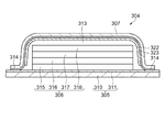
例えば、特許文献1に記載されている図12に示されるように、柔軟性を確保するためにフラットパネルディスプレイとしての有機EL装置304を薄型化し、可撓性を備えた封止フィルム307と、可撓性を備えたフィルム基板305とを、第2のポリマーフィルム311を介してシールした構成を備える有機EL装置304が提案されている。
For example, as shown in FIG. 12 described in
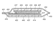
また、特許文献2では、図13に示すように、一対の薄型ガラス基板を含むガラス基板401とガラス基板437とを表面および裏面から2枚の透明な樹脂フィルム453,454で包み込んでラミネートした構造の液晶表示装置400が提案されている。つまり、液晶表示装置400は、表裏面に樹脂製の補強板が貼り付けられた状態で、2枚の樹脂フィルム454,455によってラミネートされている。上記した公知文献に記載された技術を用いることで、可撓性と強度を備えたフラットパネルディスプレイが構成されるものと考察される。
Further, in
しかしながら、上記した先行文献では、端部(辺、角)の保護は端部以外の領域と同等に、ラミネートシール等で保護する構成が用いられている。この場合、フラットパネルディスプレイが落下した場合や、基板横方向から衝撃が加えられた場合、大きな衝撃を受ける端部の保護が不十分となり、電気光学装置の信頼性が低下するという課題がある。また、上記した先行文献に示された構成を用いて、端部に加えられた衝撃に対して信頼性の確保が行える程度にまでラミネートシールを厚くすると、今度は重量の増加や、可撓性の低下が生じ、薄型テレビの一形態として撓んだ状態で表示するディスプレイや、携帯電話等の応用分野に対しての利便性が低下するという課題がある。 However, in the above-described prior art, a configuration in which end portions (sides and corners) are protected by a laminate seal or the like is used in the same manner as in regions other than the end portions. In this case, when the flat panel display is dropped or an impact is applied from the lateral direction of the substrate, there is a problem that the end portion that receives the large impact is not sufficiently protected and the reliability of the electro-optical device is lowered. In addition, if the laminate seal is thickened to such an extent that reliability can be ensured with respect to the impact applied to the end portion using the configuration shown in the above-mentioned prior document, this increases the weight and flexibility. There arises a problem that the convenience for application fields such as a display that displays in a bent state as a form of a thin television and a mobile phone is reduced.
さらに、特許文献1の段落21には、「フィルム基板305と封止フィルム307との接着部分314から密閉空間313に入り込んだとしても、乾燥剤層323によって吸着されるため、陰極318を効果的に水蒸気から保護できる」(図12参照:図番は添付図の図番に合わせて変更している)との記載がある。このように、フィルム基板305と封止フィルム307とは元々独立に形成されており、フィルム基板305と封止フィルム307との間隙は気密性が低下しやすく、信頼性が低下してしまうという課題がある。なお、引用した図面の図番は、説明の都合上元の図番とは変えている。
Further,
また、フラットパネルディスプレイとして有機EL装置等を用いる場合、有機EL装置は印加された電力を元に発光させるデバイスであるため、自己発熱により有機EL装置の温度は上昇する。特に有機EL装置に電力や信号を送受信するフレキシブル基板が備えられた領域の電力消費は激しく、この電力消費に伴う局地的な温度上昇により信頼性が低下してしまうという課題がある。 In addition, when an organic EL device or the like is used as a flat panel display, the organic EL device is a device that emits light based on applied power, and thus the temperature of the organic EL device rises due to self-heating. In particular, power consumption in a region where an organic EL device is provided with a flexible substrate for transmitting and receiving power and signals is severe, and there is a problem that reliability is lowered due to a local temperature rise accompanying this power consumption.
本発明は、上記課題の少なくとも一部を解決するためになされたものであり、以下の適用例または形態として実現することが可能である。 SUMMARY An advantage of some aspects of the invention is to solve at least a part of the problems described above, and the invention can be implemented as the following application examples or forms.
[適用例1]本適用例にかかる電気光学装置は、光が通過する片側、または光が通過する両側の材質としてガラスを用いた一対の板材と、一対の前記板材に挟持され、一対の前記板材の平面視で内側に位置する電気光学層と、一対の前記板材を挟んでラミネートする一対の樹脂フィルムと、一対の前記板材の平面視で、前記電気光学層の外側に位置する一対の前記板材の端部、または前記樹脂フィルムの端部、またはその両方の端部の少なくとも一部と、少なくとも片側の前記板材が備える、一対の前記板材の平面視で前記電気光学層の外側に位置する領域の一部と、を覆う第1封止層と、前記第1封止層の少なくとも一部を覆う、前記第1封止層よりもヤング率が高い第2封止層と、を備えることを特徴とする。 Application Example 1 An electro-optical device according to this application example is sandwiched between a pair of plate materials using glass as a material on one side where light passes or on both sides where light passes, and a pair of the plate materials. A pair of the electro-optic layers positioned inside the plate material, a pair of resin films that are laminated with the pair of plate materials sandwiched therebetween, and a pair of the electro-optical layers positioned outside the electro-optic layer in the plan view of the pair of plate materials. At least a part of the end of the plate, the end of the resin film, or both of the ends, and at least one of the plates is provided outside the electro-optic layer in plan view of the pair of plates. A first sealing layer that covers a part of the region, and a second sealing layer that covers at least a part of the first sealing layer and has a higher Young's modulus than the first sealing layer. It is characterized by.
これによれば、ヤング率が低い、即ち柔らかい第1封止層をヤング率が高い、即ち硬い第2封止層で覆うことで、応力が集中する一対の板材の端部を保護することが可能となる。硬い第2封止層で応力を分散して後、柔らかい第1封止層で応力を吸収させることで耐応力特性が向上する。また、電気光学層の外側に第1封止層および第2封止層が配置されているため、電気光学装置の機能に対して光学的に影響することがなく、光学的特性を保つことが可能となる。そのため、不透明な部材を用いることも可能となる。 According to this, by covering the first sealing layer having a low Young's modulus, that is, a soft first sealing layer with a high Young's modulus, that is, a hard second sealing layer, it is possible to protect the end portions of the pair of plate materials on which stress is concentrated. It becomes possible. The stress resistance characteristics are improved by dispersing the stress with the hard second sealing layer and then absorbing the stress with the soft first sealing layer. In addition, since the first sealing layer and the second sealing layer are disposed outside the electro-optical layer, the optical characteristics are not affected optically with respect to the function of the electro-optical device. It becomes possible. Therefore, it is possible to use an opaque member.
[適用例2]上記適用例にかかる電気光学装置であって、前記第1封止層は、ポリエチレン、エチレン−酢酸ビニル共重合体(EVA)、エチレン−メタクリル酸メチル共重合体(EMMA)、エチレン−メタクリル酸ヒドロキシアルキル共重合体、エチレン−メタクリル酸アルコキシエチル共重合体、エチレン−メタクリル酸アミノエチル共重合体、エチレン−メタクリル酸ヒドロキシグリシジル共重合体、エチレン−ビニルアルコール共重合体(EVOH)、エチレン−アクリル酸共重合体(EAA)、エチレン−メタクリル酸共重合体(EMAA)、エチレン−アクリル酸アルキル共重合体、を含むことを特徴とする。 Application Example 2 In the electro-optical device according to the application example, the first sealing layer includes polyethylene, an ethylene-vinyl acetate copolymer (EVA), an ethylene-methyl methacrylate copolymer (EMMA), Ethylene-hydroxyalkyl methacrylate copolymer, ethylene-alkoxyethyl methacrylate copolymer, ethylene-aminoethyl methacrylate copolymer, ethylene-hydroxyglycidyl methacrylate copolymer, ethylene-vinyl alcohol copolymer (EVOH) Ethylene-acrylic acid copolymer (EAA), ethylene-methacrylic acid copolymer (EMAA), and ethylene-alkyl acrylate copolymer.
上記した適用例によれば、これらの物質は80℃〜100℃程度の温度で軟化する。そして、軟化した状態では、他の物質との空隙を埋めることができ、かつ他の物質との密着性が良い。そのため、特に電気光学装置の電気光学層を樹脂封止する場合に、電気光学層の熱による劣化を防ぐことが可能となる。 According to the application example described above, these substances soften at a temperature of about 80 ° C to 100 ° C. And in the softened state, the space | gap with another substance can be filled, and adhesiveness with another substance is good. Therefore, particularly when the electro-optical layer of the electro-optical device is resin-sealed, it is possible to prevent the electro-optical layer from being deteriorated by heat.
[適用例3]上記適用例にかかる電気光学装置であって、前記第2封止層は、ポリエチレンテレフタレート、エポキシ、ポリカーボネート、ポリエチレンナフタレート、トリアセチルセルロース、環状オレフィンポリマーを含むことを特徴とする。 Application Example 3 In the electro-optical device according to the application example, the second sealing layer includes polyethylene terephthalate, epoxy, polycarbonate, polyethylene naphthalate, triacetyl cellulose, and a cyclic olefin polymer. .
上記した適用例によれば、これらの物質は上記した第1封止層と比べ高いヤング率と特に酸素、水蒸気に対して高いガスバリア性を備えている。そのため、応力が集中する一対の板材の端部を保護するとともに、耐水性を向上させることが可能となる。 According to the application example described above, these materials have a high Young's modulus and particularly a high gas barrier property against oxygen and water vapor as compared with the first sealing layer. Therefore, it is possible to protect the end portions of the pair of plate materials on which stress is concentrated and improve the water resistance.
[適用例4]上記適用例にかかる電気光学装置であって、一対の前記板材は、いずれか一方の前記板材よりも張り出した張り出し領域を備え、前記張り出し領域の他方の前記板材に向けた領域には前記電気光学層と外部とを電気的に結合させるフレキシブル基板の一端が接続され、前記樹脂フィルムによって覆われるとともに、前記フレキシブル基板の他端は外部に露出し、一対の前記板材の平面視において、前記フレキシブル基板が装着された辺の前記第2封止層は、複数本の炭素材を束にした構造を備える炭素繊維を含むことを特徴とする。 Application Example 4 In the electro-optical device according to the application example described above, the pair of plate members includes a projecting region projecting from any one of the plate materials, and the region of the projecting region facing the other plate member Is connected to one end of a flexible substrate that electrically couples the electro-optic layer and the outside, and is covered with the resin film, and the other end of the flexible substrate is exposed to the outside, and a plan view of the pair of plate members The second sealing layer on the side where the flexible substrate is mounted includes carbon fibers having a structure in which a plurality of carbon materials are bundled.
上記した適用例によれば、フレキシブル基板が位置する辺では、電気信号の展開等が行われるため、消費電力が他辺と比べ大きくなる。そこで、消費電力が大きい辺に複数本の炭素繊維を含む第2封止層を設けることで、ガスバリア性の低下を抑えて放熱性に優れた電気光学装置を提供することが可能となる。 According to the application example described above, the electric signal is developed on the side where the flexible substrate is located, so that the power consumption is larger than that on the other side. Therefore, by providing the second sealing layer including a plurality of carbon fibers on the side where the power consumption is large, it is possible to provide an electro-optical device that is excellent in heat dissipation while suppressing a decrease in gas barrier properties.
[適用例5]上記適用例にかかる電気光学装置であって、前記フレキシブル基板が装着された辺以外の少なくとも一辺に、一対の前記板材の平面視で、前記電気光学層の外側に位置する一対の前記板材の端部、または前記樹脂フィルムの端部、またはその両方の端部により構成される端部と、両側の前記板材が備える、一対の前記板材の平面視で前記電気光学層の外側に位置する領域の一部と、を覆う第1封止層と、前記端部を覆う前記第1封止層を覆う前記第2封止層と、前記端部を覆う前記第2封止層と繋がり、一対の前記板材の両側に延在する前記第2封止層を備えることを特徴とする。 Application Example 5 In the electro-optical device according to the application example described above, a pair positioned outside the electro-optical layer in a plan view of the pair of plate members on at least one side other than the side on which the flexible substrate is mounted. The end portion of the plate material, the end portion of the resin film, or the end portion constituted by both ends thereof, and the plate material on both sides are provided outside the electro-optic layer in a plan view of the pair of plate materials A first sealing layer that covers a part of the region located in the region; the second sealing layer that covers the first sealing layer that covers the end portion; and the second sealing layer that covers the end portion. And the second sealing layer extending to both sides of the pair of plate members.
上記した適用例によれば、ヤング率が低い、即ち柔らかい第1封止層をヤング率が高い、即ち硬い第2封止層で覆うことで、応力が集中する一対の板材の端部を保護することが可能となる。硬い第2封止層で応力を分散して後、柔らかい第1封止層で応力を吸収させることで耐応力特性が向上する。また、第2封止層に酸素、水蒸気に対して高いガスバリア性を備える物質を用いた場合、一対の板材の端部からの酸素、水蒸気の浸入をより少ない量に抑えることが可能となり、電気光学層の劣化を抑えることが可能となる。 According to the application example described above, by covering the first sealing layer with a low Young's modulus, that is, a soft first sealing layer with a high Young's modulus, that is, a hard second sealing layer, the ends of the pair of plate materials where stress concentrates are protected. It becomes possible to do. The stress resistance characteristics are improved by dispersing the stress with the hard second sealing layer and then absorbing the stress with the soft first sealing layer. In addition, when a substance having a high gas barrier property against oxygen and water vapor is used for the second sealing layer, it becomes possible to suppress the intrusion of oxygen and water vapor from the end portions of the pair of plate materials to a smaller amount. It becomes possible to suppress degradation of the optical layer.
[適用例6] 上記適用例にかかる電気光学装置であって、一対の前記板材の厚さは、それぞれ10μm以上、120μm以下であることを特徴とする。 Application Example 6 In the electro-optical device according to the application example described above, the thickness of the pair of plate members is 10 μm or more and 120 μm or less, respectively.
上記した適用例によれば、電気光学装置に可撓性を与えることが可能となる。10μm以上の厚さとすることで、水分や酸素に対するガスバリア性を保つことが。また、120μm以下とすることで、ガラス基板を用いた場合でも破断させることなく撓ませることが可能となる。 According to the application example described above, the electro-optical device can be given flexibility. By setting the thickness to 10 μm or more, gas barrier properties against moisture and oxygen can be maintained. In addition, when the thickness is 120 μm or less, even when a glass substrate is used, the glass substrate can be bent without being broken.
[適用例7]本適用例にかかる電気光学装置の製造方法は、光が通過する片側、または光が通過する両側にガラスを用いた矩形形状を供える一対の板材に挟まれ、一対の前記板材の平面視で内側に位置する電気光学層を備え、第1辺に前記電気光学層と外部とを電気的に結合させるフレキシブル基板を備える基板を用意する工程と、一対の樹脂フィルムにより前記基板を含む構造体を挟んでラミネートする工程と、断面形状が2層構造を備え、一方の層には第1封止層、他方の層には前記第1封止層よりも軟化点が高い第2封止層を備え、棒状の平面形状を有し、ラミネートされた前記基板の外周部と対応する辺と揃えた長さを備えた2本一組で4種類の保護体を用意する工程と、2本一組の前記保護体を前記第1封止層とラミネート材が重なる向きに、ラミネートされた前記基板と対応する辺を挟み、かつ前記基板の平面視で前記電気光学層に届かぬよう接触させる工程と、熱処理を行い、前記第1封止層を軟化させ、前記保護体とラミネートされた前記基板とを結合させる工程と、を備えることを特徴とする。 [Application Example 7] A method of manufacturing an electro-optical device according to this application example includes a pair of plate materials sandwiched between a pair of plate materials each having a rectangular shape using glass on one side where light passes or on both sides where light passes. Providing a substrate comprising an electro-optic layer positioned on the inner side in a plan view, and a flexible substrate for electrically coupling the electro-optic layer and the outside to the first side; and a pair of resin films to form the substrate. A step of laminating sandwiched structure, and a cross-sectional shape having a two-layer structure, one layer having a first sealing layer and the other layer having a higher softening point than the first sealing layer. Providing a sealing layer, having a rod-like planar shape, and preparing four types of protectors in a set of two having a length aligned with the side corresponding to the outer peripheral portion of the laminated substrate; The first encapsulating layer and the laminate material overlap the protective body in a set of two. A direction in which the side corresponding to the laminated substrate is sandwiched and contacted so as not to reach the electro-optic layer in a plan view of the substrate, and a heat treatment is performed to soften the first sealing layer, Bonding the protective body and the laminated substrate.
これによれば、一度の熱処理で、耐衝撃性に優れた電気光学装置を提供することが可能となる。また、長さが異なるのみで同一の構成を備える保護体を用いているため、保護体の形状バリエーションが不用となり、容易に製造することが可能となる。なお、ラミネートされた基板を挟むように配置する工程に代えて、片方の側にだけ保護体を配置する構成を備えていても良い。 According to this, it is possible to provide an electro-optical device having excellent impact resistance by a single heat treatment. Moreover, since the protectors having the same configuration but having different lengths are used, variations in the shape of the protectors are not required, and the manufacture can be easily performed. In addition, it may replace with the process arrange | positioned so that the laminated board | substrate may be pinched | interposed, and you may provide the structure which arrange | positions a protector only on one side.
[適用例8]上記適用例にかかる電気光学装置の製造方法であって、前記フレキシブル基板と重なる一組の前記第2封止層は複数本の炭素材を束にした構造を有する炭素繊維を含むことを特徴とする。 [Application Example 8] A method for manufacturing an electro-optical device according to the application example, wherein the pair of second sealing layers overlapping the flexible substrate are carbon fibers having a structure in which a plurality of carbon materials are bundled. It is characterized by including.
上記した適用例によれば、炭素繊維を含む封止層を用いることで、消費電力が大きいフレキシブル基板が位置する領域の熱を効果的に放熱することが可能となる。 According to the application example described above, by using the sealing layer containing carbon fibers, it is possible to effectively dissipate heat in the region where the flexible substrate with high power consumption is located.
[適用例9]本適用例にかかる電気光学装置の製造方法は、光が通過する片側、または光が通過する両側にガラスを用いた矩形形状を供える一対の板材に挟まれ、一対の前記板材の平面視で内側に位置する電気光学層を備え、第1辺に前記電気光学層と外部とを電気的に結合させるフレキシブル基板を含む基板を用意する第1工程と、一対の樹脂フィルムを前記基板を挟んでラミネートする第2工程と、ラミネートされた前記基板と勘合する、一辺を落とした矩形の断面形状を備え、内側には第1封止層、外側には前記第1封止層よりも軟化点およびヤング率が高い第2封止層を備え、一端が解放された辺の長さは前記電気光学層に届かない範囲の長さを備え、平面形状は、一辺を落とした矩形の形状を備え、一端が開放された第1辺および第2辺は、前記フレキシブル基板が接続された辺と接触する辺と揃えた長さを有し、両端が前記第1辺および前記第2辺と接続された第3辺は、前記フレキシブル基板が接続された辺と対向する辺と揃えた長さを有する第1保護体を用意する第3工程と、断面形状が2層構造を備え、一方の層には前記第1封止層、他方の層には前記第1封止層よりも軟化点が高い前記第2封止層を備え、棒状の平面形状を有し、前記フレキシブル基板が接続された辺と揃えた長さを備えた2本の第2保護体を用意する第4工程と、前記第1保護体をラミネートされた前記基板に挿入する第5工程と、2本の前記第2保護体を前記第1封止層と重なる領域に配置し、ラミネートされた前記基板の前記第1辺を挟み、かつ前記基板の平面視で前記電気光学層に届かぬよう接触させる第6工程と、熱処理を行い、前記第1封止層を軟化させ、前記第1保護体および2本の前記第2保護体と、ラミネートされた前記基板とを結合させる第7工程と、を備えることを特徴とする。 [Application Example 9] A method of manufacturing an electro-optical device according to this application example includes a pair of plate materials sandwiched between a pair of plate materials each having a rectangular shape using glass on one side where light passes or on both sides where light passes. A first step of providing a substrate including a flexible substrate that includes an electro-optic layer positioned inside in a plan view and electrically couples the electro-optic layer and the outside to a first side; and a pair of resin films, A second step of laminating the substrate, and a rectangular cross-sectional shape with one side fitted to the laminated substrate, the first sealing layer on the inside, and the first sealing layer on the outside Including a second sealing layer having a high softening point and a high Young's modulus, the length of a side whose one end is released has a length that does not reach the electro-optic layer, and the planar shape is a rectangular shape with one side dropped. A first side having a shape and having an open end; Two sides have a length aligned with a side that contacts the side to which the flexible substrate is connected, and a third side whose both ends are connected to the first side and the second side is connected to the flexible substrate. A third step of preparing a first protective body having a length aligned with a side opposite to the formed side, a cross-sectional shape having a two-layer structure, one layer including the first sealing layer and the other layer Includes the second sealing layer having a softening point higher than that of the first sealing layer, has a bar-like planar shape, and has a length aligned with the side to which the flexible substrate is connected. A fourth step of preparing a second protector, a fifth step of inserting the first protector into the laminated substrate, and two second protectors in a region overlapping the first sealing layer The first side of the laminated and laminated substrate is sandwiched, and reaches the electro-optic layer in a plan view of the substrate. A sixth step of bringing into contact with each other and a heat treatment to soften the first sealing layer, and to bond the first protective body and the two second protective bodies to the laminated substrate. And a process.
これによれば、一度の熱処理で、耐衝撃性に優れた電気光学装置を提供することが可能となる。また、平面形状として一辺を落とした矩形状の第1保護体を用いることで、実装回数を減らすことが可能となる。なお、第3工程は第6工程以前であれば良く工程順序の変更が可能である。また、第5工程の後で一旦第7工程を行い、改めて第6工程の後で再び第7工程を行っても良い。また、第4工程の次に第7工程を行い、改めて第5工程と第7工程を繰り返しても良い。また、最終的に第1保護体、第2保護体、ラミネートされた基板とを一体化すべく結合させることができる状態を実現できる範囲の工程であれば、上記した製造工程中に割り込ませても良い。また、第4工程で用意する2本の第2保護体に代えて一本の第2保護体とし、第6工程で挟む工程に代えて片側に置く構成を用いても良い。 According to this, it is possible to provide an electro-optical device having excellent impact resistance by a single heat treatment. Moreover, it becomes possible to reduce the frequency | count of mounting by using the rectangular 1st protector which dropped one side as a planar shape. In addition, the 3rd process should just be before a 6th process, and can change a process order. Alternatively, the seventh step may be performed once after the fifth step, and the seventh step may be performed again after the sixth step. Alternatively, the seventh step may be performed after the fourth step, and the fifth step and the seventh step may be repeated. Moreover, if it is the process of the range which can implement | achieve the state which can be finally combined with the 1st protector, the 2nd protector, and the laminated board | substrate, it may interrupt during the above-mentioned manufacturing process. good. Moreover, it may replace with two 2nd protectors prepared at a 4th process, and it may be set as one 2nd protector, and it may replace with the process pinched | interposed at a 6th process, and the structure put on one side may be used.
[適用例10]上記適用例にかかる電気光学装置の製造方法であって、前記第2保護体の前記第2封止層は、複数本の炭素材を束にした構造を有する炭素繊維を含むことを特徴とする。 Application Example 10 In the method of manufacturing the electro-optical device according to the application example, the second sealing layer of the second protective body includes carbon fibers having a structure in which a plurality of carbon materials are bundled. It is characterized by that.
上記した適用例によれば、炭素繊維を含む封止層を用いることで、消費電力が大きいフレキシブル基板が位置する領域の熱を効果的に放熱することが可能となる。 According to the application example described above, by using the sealing layer containing carbon fibers, it is possible to effectively dissipate heat in the region where the flexible substrate with high power consumption is located.
[適用例11]本適用例にかかる電子機器は、上記適用例にかかる電気光学装置または電気光学装置の製造方法で製造された電気光学装置を備えたことを特徴とする。 Application Example 11 An electronic apparatus according to this application example includes the electro-optical device manufactured by the electro-optical device or the electro-optical device manufacturing method according to the application example.
これによれば、可撓性を備え、かつ耐衝撃性に優れた電気光学装置を備えていることから、曲面形状を覆うことを可能とし、かつ信頼性に優れたモバイル表示装置等の電子機器を提供することが可能となる。 According to this, since the electro-optical device having flexibility and excellent impact resistance is provided, it is possible to cover a curved surface shape, and an electronic device such as a mobile display device having excellent reliability. Can be provided.
(第1の実施形態:電気光学装置の構成−1)
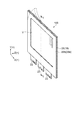
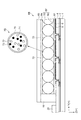
以下、電気光学装置の構成について図面を用いて説明する。図1は電気光学装置の構造を示す斜視図、図2は、図1に示す斜視図のf−f線断面図である。ここでは、フラットパネルディスプレイとして有機EL装置を用いた例について説明する。なお、有機EL装置以外の応用に対しても対応可能であり、例えば液晶装置や電子ペーパーに対しても対応可能である。また、有機EL装置を用いた照明等の用途にも転用することが可能である。特に無影灯や、光の照射パターンを調整可能な光源として好適である。有機EL装置、液晶装置、電子ペーパー等に応用する場合の対応については後述する。
First Embodiment: Configuration of Electro-Optical Device-1
Hereinafter, the configuration of the electro-optical device will be described with reference to the drawings. 1 is a perspective view showing the structure of the electro-optical device, and FIG. 2 is a cross-sectional view taken along the line ff of the perspective view shown in FIG. Here, an example in which an organic EL device is used as a flat panel display will be described. In addition, it can respond also to applications other than an organic EL apparatus, for example, can respond also to a liquid crystal device and electronic paper. Further, it can be diverted to uses such as lighting using an organic EL device. It is particularly suitable as a light source capable of adjusting a shadowless lamp or a light irradiation pattern. The correspondence when applied to an organic EL device, a liquid crystal device, electronic paper or the like will be described later.
表示パネル18は、一対の板材の一方としての素子基板1と、一対の板材の他方としてのCF(カラーフィルター)基板16を含み、通常無アルカリガラスで構成されている。また、素子基板1とCF基板16に挟まれる後述する図3に示す有機EL層8とを含んでいる。
The
ここで、図2に示すように、CF基板16から素子基板1に向かう方向を第1方向とし、素子基板1からCF基板16に向かう方向を第2方向として説明を続ける。
Here, as shown in FIG. 2, the description is continued with the direction from the
素子基板1の第1方向側には、接着層26aが備えられている。そして、接着層26aの第1方向側には、複数本の炭素材を束にした形状を備える炭素繊維を含む樹脂等を用いた放熱層27が備えられている。素子基板1と放熱層27とは、接着層26aにより素子基板1と固着されている。
An
また、放熱層27の第1方向側には、接着層26bが備えられている。そして、接着層26bの第1方向側には、保護フィルム28aが備えられている。保護フィルム28aは、接着層26bにより放熱層27と固着されている。また、CF基板16の第2方向側には、接着層26cが備えられている。そして、接着層26cの第2方向側には、保護フィルム28bが備えられている。保護フィルム28bは、接着層26cにより固着されている。
An
換言すれば、保護フィルム28a,28bによってラミネートされた構造を備えている。なお、以下の説明において、保護フィルム28a,28bによってラミネートされた状態の表示パネル18のことをラミネート構造体25とも記載する。
In other words, a structure laminated with the
表示パネル18は、一対の板材の一方としての素子基板1と、一対の板材の他方としてのCF基板16を備えている。また表示パネル18全面を覆うように配置された接着層26a〜26cには、素子基板1、CF基板16、および保護フィルム28a,28bとの接着性、柔軟性、透明性(光取り出し性)、フレキシブル基板23のモールド性(絶縁性と耐熱性)等の条件を満たす機能が必要となる。
これらの機能を満たすため、接着層26a〜26cの材料として、耐水性(低吸水率)や絶縁性、柔軟性、透明性、低温溶着性を有するポリエチレンや、エチレン−酢酸ビニル共重合体(EVA)等をベースとした樹脂を用いている。また、保護フィルム28a,28bに用いる樹脂には、透明性と耐水性が重視される。具体的にはポリエチレンテレフタレート(PET)や、ポリカーボネート等を用いることが好適である。
The
In order to satisfy these functions, as the material of the
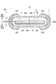
表示パネル18は、マトリックス状に配置された複数の画素を含む表示領域Vを備えている。また、柔軟性を確保するために、表示パネル18を構成する、一対の板材としての素子基板1、CF基板16の厚さは、それぞれ10μm以上120μm以下に設定されている。表示領域Vには、赤色(R)、緑色(G)、青色(B)の各色画素が周期的に配置されており、各画素が出射する表示光によりフルカラーの画像が表示される。なお、カラー表示を行う表示パネルに限定するものではなく、モノクロ表示を行う表示パネルであっても良い。また、照明等の光源としても適用可能である。表示領域Vは、一辺が、この一辺と端で接続される2辺よりも長い(図1の場合では図面の横方向が長い)長方形をなしており、図1を含む各図においては、当該横方向をX軸方向とし、横方向よりも短い縦方向をY軸方向と定義している。また、表示パネル18の厚さ方向をZ軸方向としている。また、表示領域V側の面を第1の面としての表面、その反対側の面を第2の面としての裏面という。また、表示領域Vは正方形でも良い。
The
ここで、ラミネート構造体25の表面(表示領域V側)および裏面には、平面的に表示領域Vを囲う額縁状の第1封止層としての第1補強部材29aと、第2封止層として第2補強部材29bが取り付けられている。額縁状とは、表示領域Vに開口部を有するようにラミネート構造体25を覆う構成である。さらに、第1補強部材29aおよび第2補強部材29bの開口部の形状は表示領域Vの外側とラミネート構造体25の端部との間に設けられており、第1補強部材29aの端部は、ラミネート構造体25の端部を覆う構成が好ましい。このようにすることで表示パネル18への大気中の水分や酸素の浸入が抑えられるため、信頼性が向上する。
Here, on the front surface (display region V side) and the back surface of the
第2補強部材29bは、衝撃等による応力に耐えうる部材であることが好ましい。樹脂としては、例えばポリエチレンテレフタレート、エポキシ、ポリカーボネート、ポリエチレンナフタレート、トリアセチルセルロース、環状オレフィンポリマーを含む樹脂が好適である。これらの物質は高いヤング率(剛性)と特に酸素、水蒸気に対して高いガスバリア性を備えている。そのため、応力が集中する端部を保護するとともに、耐水性を向上させることが可能となる。
The second reinforcing
そして、第1補強部材29aは、第2補強部材29bに加えられた応力を分散させ、ラミネート構造体25に加わる応力を低減させる樹脂を用いることが好適である。例えばポリエチレン系共重合体として、ポリエチレン、エチレン−酢酸ビニル共重合体(EVA)、エチレン−メタクリル酸メチル共重合体(EMMA)、エチレン−メタクリル酸ヒドロキシアルキル共重合体、エチレン−メタクリル酸アルコキシエチル共重合体、エチレン−メタクリル酸アミノエチル共重合体、エチレン−メタクリル酸ヒドロキシグリシジル共重合体、エチレン−ビニルアルコール共重合体(EVOH)、エチレン−アクリル酸共重合体(EAA)、エチレン−メタクリル酸共重合体(EMAA)、エチレン−アクリル酸アルキル共重合のうち、いずれかを用いることが好ましい。または、これらを2つ以上組み合わせた共重合体、または混合物を含むものが好適である。これらの物質は、第2補強部材29bで挙げた樹脂と比べ、ヤング率が低い、即ち柔らかい。そのため、応力を吸収する機能を備え、ラミネート構造体25に加わる応力を低減させることで信頼性を向上させることが可能となる。
The first reinforcing
なお、図2に示すように、表示パネル18は、一対の板材の一方としての素子基板1と、一対の板材の他方としてのCF(カラーフィルター)基板16とから構成されており、その一端には、素子基板1の一辺がCF基板16から張出した張出し領域が形成されている。張出し領域には、フレキシブル基板23が接続されている。なお、フレキシブル基板23とは、フレキシブルプリント回路基板の別称である。また、フレキシブル基板23には、駆動用IC(Integrated Circuit)21が実装され、その端部には外部機器と接続するための複数の端子が形成されている。ここで、フレキシブル基板23が接続されるラミネート構造体25の辺は、信号のやり取りや電力の伝達等により、消費電力が高くなっている。そのため、放熱性が高い部材を用いることが好適である。具体的には、第2補強部材29b’として炭素繊維樹脂等を用いることが好適である。炭素繊維樹脂を用いた場合、熱伝導率が20〜60W/m・kと、ガラス(1W/m・k)や汎用プラスチック(約0.5W/m・k)に比べて高くなるため、十分な放熱性を得ることができる。このような構成により、表示装置100は、図1において点線で示したように、曲げることが可能なフレキシブル性と、曲げても表示パネル18が割れない実用強度とを兼ね備えることを可能としている。そして、他の辺には、例えばPET樹脂を用いた第2補強部材29bを配置することで、耐衝撃性を向上させることが可能となる。
As shown in FIG. 2, the
フレキシブル基板23の表面には、接着層26cが備えられ、接着層26cを介して保護フィルム28b、が貼り付けられている。そして、フレキシブル基板23の裏面には、接着層26bを介して放熱層27が貼り付けられている。そして、放熱層27と重ねて接着層26aが備えられ、保護フィルム28aが貼り付けられている。
An
そして、第1補強部材29aが、ラミネート構造体25の端部と重なるように配置されている。そのため、ラミネート構造体25の封止特性が向上し、水分の浸入等による劣化をより抑えることが可能となる。さらに、第2補強部材29b,29b’が、第1補強部材29aを介してラミネート構造体25と貼り付けられている。そのため、より高い耐衝撃性が得られている。なお、ここでは第2補強部材29b,29b’をラミネート構造体25の両面に備えた例について説明したが、これは片面のみに配置させても良い。この場合、製造工程を短縮させることが可能となる。また、フレキシブル基板23が接続されるラミネート構造体25の辺にも他の辺と同様、上記した第2補強部材29bと揃えた樹脂を配置しても良く、この場合にも製造工程の短縮が可能となる。
The first reinforcing
(電気光学装置の構成−2)
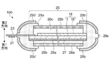
続けて、有機EL装置を用いた例について封止層近傍の構成について説明する。図3は、図2の表示パネル18におけるd部の拡大図である。以下、ラミネート構造体25のd部について説明を行う。ラミネート構造体25は、表示パネル18を含んでいる。そして表示パネル18は、素子基板1、素子層2、駆動トランジスター3、平坦化層4、反射層5、画素電極6、隔壁7、電気光学層としての有機EL層8、共通電極9、電極保護層10、緩衝層11、ガスバリア層12、充填材13、CF層14、封止層15、CF基板16等を含んでいる。
(Configuration of electro-optical device-2)
Next, the configuration in the vicinity of the sealing layer will be described for an example using an organic EL device. FIG. 3 is an enlarged view of a portion d in the
また、素子基板1とCF基板16とに挟持された部位のことを機能層17という。換言すれば、素子層2からCF層14までの積層構造を機能層17という。素子基板1は、透明な無機ガラスから構成されている。本実施形態では、好適例として、無アルカリガラスを用いている。素子層2には、各画素をアクティブ駆動するための画素回路を備えている。画素回路は、画素を選択するための選択トランジスターとなるTFT(Thin Film Transistor)や、有機EL層8に電流を流すための駆動トランジスター3等を備えている。なお、本実施形態では、封止層15近傍まで表示に寄与するよう記載しているが、状況により、フォトリソグラフ工程等の均一性を確保するため、封止層15近傍はダミーエリアとし、表示に用いない場合もある。本実施形態では、表示に寄与する場合を想定している。
A portion sandwiched between the
素子層2の上層(Z軸(−)方向)には、例えば、アクリル樹脂などからなる絶縁層である平坦化層4が形成されている。平坦化層4の上層には、画素ごとに区画されて、反射層5と、画素電極6とがこの順番で積層されている。反射層5は、例えば、アルミニウム等を用いた反射層であり、有機EL層8から素子基板1側に向かう光を反射して、表示に寄与する光にする。画素電極6は、ITO(Indium Tin Oxide)や、ZnO等の透明電極から構成されており、画素ごとに素子層2の駆動トランジスター3のドレイン端子と平坦化層4を貫通するコンタクトホールにより接続されている。隔壁7は、光硬化性の黒色樹脂などから構成され、平面的に各画素を格子状に区画している。なお、素子層2における駆動トランジスター3を含む画素回路は、光による誤動作を防止するために、平面的に隔壁と重なるように配置されている。
In the upper layer (Z-axis (−) direction) of the
有機EL層8は、画素電極6、および隔壁7を覆うよう配置されている。また、図3においては一層の構成となっているが、実際は、それぞれが有機物の薄膜からなる正孔輸送層、発光層、電子注入層などから構成されており、画素電極6上にこの順番に積層されている。正孔輸送層は、芳香族ジアミン(TPAB2Me−TPD,α−NPD)などの昇華性の材料から構成されている。発光層は、赤、緑、青の3色を組み合わせて形成される白色光を放射する多層からなる有機発光材料薄膜から構成されている。電子注入層は、LiF(フッ化リチウム)などから構成されている。共通電極9は、MgAgなどの金属を、光を透過するようにごく薄く成膜した金属薄膜層である。さらに、抵抗を下げるため、ZnOなどの金属酸化物やTiNなどの金属窒化物層など透明導電膜を積層しても良い。
The
電極保護層10は、SiO2や、Si3N4、SiOxNyなどの透明、かつ、高密度で、水分を遮断する機能を有する材質から構成されている。緩衝層11は、熱硬化性のエポキシ樹脂などの透明な有機緩衝層である。ガスバリア層12は、SiO2や、Si3N4、SiOxNyなどの透明、かつ、高密度で、水分を遮断する機能を有する封止層であり、有機EL層8への水分の浸入を防止する機能を担う。充填材13は、例えば、熱硬化性のエポキシ樹脂などからなる透明な接着層であり、ガスバリア層12とCF層14との間の凹凸面に充填されるとともに、両者を接着する。また、外部から、有機EL層8への水分の浸入を防ぐ機能も果たす。
The electrode
CF基板16は、素子基板1と同様な無機ガラスから構成されており、有機EL層8側(Z軸(+)側)には、CF層14が形成されている。CF層14には、赤色カラーフィルター14r、緑色カラーフィルター14g、青色カラーフィルター14bが画素配置と同様に配置されている。詳しくは、各色のカラーフィルターは、それぞれが対応する画素電極6と重なるように配置されており、各カラーフィルター間には、ハッチングで示した遮光部が形成されている。遮光部は、平面的に隔壁7と重なるように格子状に形成されており、光学的には、ブラックマトリックスの機能を果たす。
The
このように構成された各画素からは、カラーフィルターの色調に対応した表示光が出射される。例えば、赤色画素の場合、有機EL層8で放射された白色光は、赤色カラーフィルター14rによって赤色光が選択されて、赤色の表示光としてCF基板16から出射される。また、緑色、青色の画素においても同様である。これにより、表示領域Vでは、CF基板16から出射される複数のカラー画素からの表示光によりフルカラーの画像が表示されることになる。
From each pixel configured in this manner, display light corresponding to the color tone of the color filter is emitted. For example, in the case of a red pixel, white light emitted from the
また、反射層5を無くせば、表示領域Vの裏面においても表示を行うことができる。換言すれば、表示パネル18の表裏両面において表示を行うことができる。なお、表示パネル18の構成は、トップエミッション型に限定するものではなく、2枚のガラス基板間に、電気光学層を挟持した構成であれば良い。例えば、有機EL層8が発する光を素子基板1側から出射するボトムエミッション型の有機EL表示装置であっても良い。また、無機ELを光源として備えた無機EL表示装置であっても良い。また、透過型や反射型の液晶装置を用いても良い。加えて、電子ペーパーとも称される表示装置を用いても良い。さらに、蛍光灯等を代替する照明用に用いても良い。
Further, if the
また、素子基板1の一辺がCF基板16から張出した張出し領域には、フレキシブル基板23が接続されている。フレキシブル基板23は、例えば、ポリイミドフィルムの基材に銅箔などの配線パターンが形成され、当該パターン上に、ドライバーIC等が実装された柔軟性を有する基板であり、素子基板1に形成された透明電極との間で、異方性導電接着フィルムなどにより、電気的な接続が取られている。ここで、樹脂フィルム25a(図8参照)を接着剤(充填材)として機能させることによって、フレキシブル基板23と素子基板1との間で十分な密着性と柔軟性とを確保している。ここで、接着層26aは、表示パネル18と放熱層27とを貼り合わしている。そして、接着層26bは、放熱層27と保護フィルム28aとを貼り合わしている。そして、接着層26cは表示パネル18と保護フィルム28bとを貼り合わしている。
In addition, a
(電気光学装置の構成−3)
続けて、有機EL装置を用いた例について封止層近傍の構成について再度図2、図3を用いて説明する。ここでは、表示装置100がフレキシブル性と、端部が受ける衝撃に対しての実用強度(強靭さ)とを両立させるために必要な各部の寸法について説明する。
まず、表示パネル18の厚さについて説明する。図3では、各構成部位の積層関係を明確にするために、特に、機能層17における縮尺を他の部位よりも拡大しているが、実際は、機能層17の部分が最も薄く構成されることになる。機能層17の厚さは、数μm〜20μm程度の厚さである。このうち、緩衝層11が半分以上の厚さを占めている。ちなみに、厚さがnmオーダーの複数の薄膜からなる有機EL層8の厚さは1μmに満たない。なお、図3で説明した通り、表示パネル18は、フレキシブル性に耐えられる接着強度を得るため、樹脂フィルム25a,25bにより埋められている。即ち基板間に中空構造を持たない全固体物質で充填されている。
(Configuration of electro-optical device-3)
Next, the configuration in the vicinity of the sealing layer will be described again with reference to FIGS. 2 and 3 for an example using the organic EL device. Here, the dimensions of each part necessary for the
First, the thickness of the
本実施形態では、好適例として、図2に示す素子基板1およびCF基板16の厚さをそれぞれ約40μmとしている。また、表示パネル18の総厚は、好適例として約90μmとしている。発明者等の実験結果によれば、有機ELパネルの信頼性を確保するためには、ガスバリア層12などの封止構造に加えて、素子基板1およびCF基板16の厚さが約10μm以上必要であることが解っている。換言すれば、素子基板1およびCF基板16の厚さを各々約10μm以上に設定することによって、フレキシブル性に耐えられるだけの衝撃強度と、十分な防湿性を確保することが可能となる。
他方、素子基板1、およびCF基板16の厚さが約120μm以上となると、柔軟性が損なわれて来ることも解っている。このため、素子基板1、およびCF基板16の厚さは、10μm以上120μm以下に設定することが好ましい。また、強度と柔軟性とのバランスを考慮すると、20μm以上80μm以下とすることがより好ましい。そして、素子基板1とCF基板16とを重ね合せた表示パネル18の総厚は、強度と柔軟性とのバランスを考慮して、50μm以上200μm以下に設定することが好ましい。
In the present embodiment, as a suitable example, the thicknesses of the
On the other hand, when the thickness of the
なお、素子基板1、およびCF基板16は、それぞれが初期段階で0.3mm以上1mm以下程度の厚さであったものを研磨、またはエッチングして薄くしたものである。好適には、表裏のガラス基板が厚い状態の表示パネルを製造した後、フッ酸(フッ化水素酸)を溶解したエッチング溶液(水溶液)として用いたエッチングにより、所期の厚さの表示パネル18を製造する。なお、この方法に限定するものではなく、所期の厚さの表示パネル18を形成可能な方法であれば良く、例えば、機械的研磨法を用いることであっても良い。
Note that the
次に、再び図2を参照して、ラミネート構造体25を構成する樹脂フィルム25a,25bの厚さについて説明する。本実施形態では、好適例として、厚さが約50μmのEVAフィルムを樹脂フィルム25a,25bに用いている。発明者等の実験結果によれば、表示パネル18の周縁部における隙間を含む段差の被覆性(充填性)を満たすためには、約20μm以上の厚さが必要となることが解っている。この被覆性と、表示装置100としての総厚とのバランスを考慮すると20μm以上100μm以下であることが好ましい。また、樹脂フィルムのコストや、ラミネートのし易さ(作業性)を加味すると、40μm以上80μm以下であることが好ましい。
Next, referring to FIG. 2 again, the thickness of the
次に、第1補強部材29a,29bの厚さについて説明する。第1補強部材29aは、緩衝能力を確保させるためには、40μm以上120μm以下程度の範囲内にあることが好ましい。そして、第2補強部材29bは、応力を分散し、可撓性を確保させるためには、40μm以上120μm以下程度の範囲内にあることが好ましい。なお、上記好適例の寸法は、発明者等が実験結果や、物性データなどから創意工夫の末に導出した好適事例の一つであり、これに限定するものではなく、この値以外の寸法を用いても差し支えない。例えば表示装置100の柔軟性を重視する場合、各領域を薄くすることが好適となり、表示装置100の耐衝撃性を重視する場合、各領域を厚くすることが好適となる。
Next, the thickness of the first reinforcing
(第2の実施形態:補強部材の別の構成)
以下、第2の実施形態として、補強部材の別の構成について説明する。フレキシブル基板23を含まない部分では、より気密性と保護機能に優れた第1補強部材29a,29bを構成することが可能である。図4は、別の構成を備えた補強部材を含む表示装置の断面図である。第1の実施形態と異なる主な点としては、第2補強部材29bがラミネート構造体25の端部を覆っている点である。
(2nd Embodiment: Another structure of a reinforcement member)
Hereinafter, another configuration of the reinforcing member will be described as a second embodiment. In the portion not including the
このような構造を用いることで、ヤング率が低い、即ち柔らかい第1封止層としての第1補強部材29aを、ヤング率が高い、即ち硬い第2封止層としての第2補強部材29bで覆うことで、応力が集中するラミネート構造体25の端部を保護することが可能となる。即ち、硬い第2補強部材29bで応力を分散して後、柔らかい第1補強部材29aで応力を吸収させることで耐応力特性が向上する。また、硬い第2補強部材29bに酸素、水蒸気に対して高いガスバリア性を備える、例えばポリエチレンテレフタレート樹脂、エポキシ樹脂、ポリカーボネート樹脂を含む物質を用いた場合、ラミネート構造体25の端部からの酸素、水蒸気の浸入をより少ない量に抑えることが可能となり、電気光学層としての有機EL層8の劣化を抑えることが可能となる。
By using such a structure, the first reinforcing
(第1の変形例)
以上、ラミネート構造体25の端部を補強する構成について説明したが、上記した例に対して別の構成を備えていても良い。以下、構成が一部異なる構成について説明する。上記した例では、図2、図4等に示すように、第2補強部材29bは、ラミネート構造体25の端部を覆う、もしくは表裏面に配置されているが、これは片面のみにあっても良く、この場合には製造工程を短縮することが可能となる。なお、この場合においても、第1補強部材29aはラミネート構造体25の端部を覆うことが好ましい。
(First modification)
The configuration for reinforcing the end portion of the
また、ラミネート構造体25として、表示パネル18を保護フィルム28a,28bで全て覆っている例について説明したが、これは図5に示すように表示パネル18の端部が露出する構成を備えていても差し支えない。この領域は第1補強部材29a、第2補強部材29bで覆われるため気密性と強度とを保つことが可能となる。また、このような構成をとることで、端部よりはみ出す部分を小さくすることが可能となり表示に寄与しない額縁領域を狭くすることが可能となる。さらに、ラミネート条件によっては、表示パネル18の端部が保護フィルム28a,28bに加え、接着層26b,26cが露出する場合があるが、本実施形態に示すように、第1補強部材29a、第2補強部材29b等を含めて端部の機械的強度を高めている上、気密性も付加しているため、信頼性を向上させることが可能となる。
Moreover, although the example which covered the
また、上記した例では、表示パネル18に有機EL装置を用いた例について説明したが、これは液晶装置やEPD(電子ペーパー)等を用いても良い。以下液晶装置とEPDを用いる場合の構造について簡単に説明する。まず、典型的な液晶装置について説明する。
In the above example, an example in which an organic EL device is used for the
図6(a),(b)は各々、本発明を適用した表示装置100を各構成要素と共に対向基板の側から見た平面図、およびそのH−H’断面図である。図6(a),(b)に示すように、液晶を用いた表示装置100では、素子基板1と対向基板20(一対の基板)とにより液晶層50を挟持している。より詳細には、素子基板1に形成されたストッパー層110aと、対向基板20に形成されたストッパー層110bと、によりシール材107を挟むように貼り合わされている。
6A and 6B are a plan view of the
シール材107は、光硬化樹脂や熱硬化性樹脂等を用いた接着剤であり、両基板間の距離を所定値とするためのグラスファイバー、あるいはガラスビーズ等のギャップ材が配合されている。本形態において、素子基板1の基体は透光性基板10dであり、対向基板20の基体も、同様な透光性基板20dである。
The sealing
素子基板1において、シール材107の外側領域では、素子基板1の一辺に沿ってデータ線駆動回路101および複数の端子102が形成されており、この一辺に隣接する他の辺に沿って走査線駆動回路104が形成されている。また、対向基板20のコーナー部の少なくとも1箇所においては、素子基板1が備える共通電極COMと、対向基板20が備える共通電極24と、の間で電気的導通をとるための上下導通材109が形成されている。
In the
素子基板1には、アルミニウムを用いた反射性の画素電極9a(反射性電極)がマトリックス状に形成されている。画素電極9aと斜方蒸着層18aとの間に電極保護層111を挟むことが好適である。電極保護層111としては窒化酸化珪素層や、酸化チタン層を用いることができる。なお、(18a)で示される領域は、斜方蒸着層18aの製造工程において寄生的に生じた領域であり、特別な機能を有するものではない。
On the
対向基板20には、シール材107の内側領域に遮光性材料を用いた額縁108が備えられており、その内側が画像表示領域10aとされている。対向基板20には、ITO(Indium Tin Oxide)層等を用いた共通電極24が備えられている。なお、対向基板20に、画素電極9aの隙間と対向する位置にブラックマトリックスあるいはブラックストライプと称せられる遮光層(図示せず)を形成しても良い。なお、画素領域10bには、額縁108と重なる領域にダミーの画素が構成される場合があり、この場合、画素領域10bのうち、ダミー画素を除いた領域が画像表示領域10aとして利用されることになる。
The
液晶を用いてなる反射型の表示装置100においては、対向基板20の側から入射した光が画素電極9aで反射して再び、対向基板20の側から出射される間に液晶層50によって画素毎に光変調される結果、画像が形成される。ここで、液晶を用いた表示装置100は、モバイルコンピューター、携帯電話機といった電子機器のカラー表示装置として用いることができ、この場合、対向基板20には、カラーフィルター(図示せず)や保護層が形成される。
In the
次に、典型的なEPDについて説明する。図7は、本実施形態にかかる反射型の電気泳動パネルである。反射型の電気泳動パネルとしての表示パネル68は、素子基板1と対向基板65との間に電気泳動層67を挟持した構成なっている。また、素子基板1から画素電極6までの積層構造は、図3の構成と同一である。
対向基板65は、例えばガラスやプラスチック等からなる透明な基板である。対向基板65における素子基板1側には、対向電極64が複数の画素電極6と対向して全面(ベタ状)に形成されている。対向電極64は、ITO等の透明導電材料から形成されている。
Next, typical EPD will be described. FIG. 7 is a reflection type electrophoresis panel according to the present embodiment. A
The
電気泳動層67は、複数のマイクロカプセル70、複数のマイクロカプセル70を保持するバインダー62、および接着層61などから構成されている。なお、表示パネル68は、電気泳動層67が予め対向基板65側にバインダー62によって固定されてなる電気泳動シートと、当該シートとは別途製造され、画素電極6などが形成された素子基板1とを、接着層61により接着することによって形成されている。
The
マイクロカプセル70は、画素電極6、および対向電極64間に挟持され、1つの画素内に(言い換えれば、1つの画素電極6に対して)1つまたは複数配置されている。そして、図7右上の拡大図に示すように、マイクロカプセル70は、被膜75の内部に分散媒71と、複数の白色粒子72と、複数の黒色粒子73とを封入した構成となっている。マイクロカプセル70は、例えば、50μm程度の粒径を有する球状に形成されている。被膜75は、アクリル樹脂、ユリア樹脂、アラビアガム、ゼラチン等の透光性を有する高分子樹脂から形成されている。分散媒71は、白色粒子72および黒色粒子73をマイクロカプセル70内(言い換えれば、被膜75内)に分散させる媒質である。白色粒子72は、例えば、二酸化チタン、亜鉛華(酸化亜鉛)、三酸化アンチモン等の白色顔料からなる粒子(高分子或いはコロイド)であり、例えば負に帯電されている。黒色粒子73は、例えば、アニリンブラック、カーボンブラック等の黒色顔料からなる粒子(高分子或いはコロイド)であり、例えば正に帯電されている。
One or a plurality of
これにより、白色粒子72および黒色粒子73は、画素電極6と対向電極64との間の電位差によって発生する電場(電位差)によって分散媒71中を移動するため、対向電極64側に集まった粒子の色調が表示されることになる。
As a result, the
なお、白色粒子72、黒色粒子73に用いる顔料を、例えば赤色、緑色、青色等の顔料に代えることによって、赤色、緑色、青色などのカラー表示をすることもできる。また、上述したマイクロカプセル方式に限定するものではなく、帯電性を有する電子粉流体を画素内に入れ、プラス・マイナスを切り替えることで表示の切り替え・オンオフを制御する電子粉体方式の電気泳動パネルであっても良い。または、コレステリック液晶を用いた電気泳動パネルであっても良い。
In addition, color display of red, green, blue, etc. can also be performed by changing the pigment used for the
(第3の実施形態:電気光学装置の製造方法−1)
以下、電気光学装置の製造方法について説明する。図8(a),(b)、図9(a),(b)は電気光学装置の製造方法を説明するための工程斜視図である。
(Third Embodiment: Electro-Optical Device Manufacturing Method-1)
Hereinafter, a method for manufacturing the electro-optical device will be described. FIGS. 8A, 8B, 9A, and 9B are process perspective views for explaining a method of manufacturing the electro-optical device.
まず、図8(a)に示すように、各部材を重ね合わせた状態とし、ラミネート装置にセットする。詳しくは、樹脂フィルム25b上に、表示パネル18と、樹脂フィルム25aと、補強部材28とを、この順番で重ね合わせる。なお、図8(a)では省略しているが、各部材の重ね合わせは専用の案内板を用いて行われ、平面的な位置合わせもなされている。この工程は、好適例としては、通常減圧環境下で行うが、常圧環境下で行っても良い。また、一層毎に貼り合わせ、複数回貼り合わせる工程を用いても良く、この場合には貼り合わせる条件(温度、圧力、時間等)を個別に設定することができ、各部材を最適な条件(しわ、厚さムラ、剥がれ等が発生しにくい条件)で貼り合わせることが可能となる。
そして、準備体をラミネート装置にセットする。図8(a)では、ラミネート装置の加圧ローラー81,82のみを図示している。
First, as shown in FIG. 8 (a), the respective members are superposed and set in a laminating apparatus. Specifically, the
Then, the preparation is set in the laminating apparatus. FIG. 8A shows only the
次に、ラミネート装置が設置された環境を減圧し、減圧環境とする。なお、ラミネート装置は、内部環境を所望の気圧環境に設定可能なチャンバー装置(室)内に設置してある。この工程によって、内部の空気(気泡)が除去(脱泡)される。また、並行して、加圧ローラー81,82を80℃〜120℃程度に加熱する。
次に、図8(b)の矢印で示すように、フレキシブル基板23の反対側の一辺から、一対の加圧ローラー81,82の間に挿入して、ラミネート工程を行う。加圧ローラー81,82に挟持された部分では、ローラーの熱によって樹脂フィルム25a,25bが溶解し、さらに加圧されて相互に接着される。また、溶解した樹脂フィルムは、接着剤(充填材)として機能し、表示パネル18、フレキシブル基板23、および補強部材28も接着する。
また、各部材を走査するようにラミネートが行われるため、各部材に気泡(空気)が残っていたとしても、気泡は、ラミネート順に沿って他端側に押し出されることになる。そして、図8(b)に示すように、ラミネートされた表示装置100が加圧ローラー81,82間から押し出されてラミネートが完了する。
Next, the environment where the laminating apparatus is installed is depressurized to form a depressurized environment. The laminating apparatus is installed in a chamber apparatus (room) that can set the internal environment to a desired atmospheric pressure environment. By this step, the internal air (bubbles) is removed (defoamed). In parallel, the
Next, as shown by the arrow in FIG. 8B, a laminating process is performed by inserting between a pair of
Further, since the lamination is performed so that each member is scanned, even if bubbles (air) remain in each member, the bubbles are pushed out to the other end side in the order of lamination. Then, as shown in FIG. 8B, the
次に、ラミネート処理で発生した残留応力を取り除くためにアニーリング処理を行う。アニーリング処理は、引き続き減圧環境で行っても良いし、通常環境下で行っても良い。特に、樹脂フィルム25a,25bが架橋成分を含む場合には、約90℃でアニーリング処理し、架橋を完全なものとすることが好ましい。
Next, an annealing process is performed to remove the residual stress generated in the laminating process. The annealing process may be performed continuously in a reduced pressure environment or in a normal environment. In particular, when the
次に、第1補強部材29aと第2補強部材29bとを重ねた棒状(薄板形状)を備えた部材を、表示領域Vを囲う額縁状の領域に対して、ラミネート構造体25の端部と、ラミネート構造体25の端部と連結しており、表示領域Vを覆わない額縁状の開口を挟持するよう、第1補強部材29a側を接触させるよう2本一組で配置する。ここまでの工程を終えた状態での断面図を図9(a)に示す。
Next, a member having a bar shape (thin plate shape) in which the first reinforcing
次に、図9(b)に示すように再びラミネート処理を行い、第1補強部材29aにより空隙を埋めることで、図1、図2に示される表示装置100が形成される。ここで、フレキシブル基板23が配置されている辺には、炭素繊維樹脂を用いることも好適であり、消費電力が大きい領域(発熱量が多い)からの放熱を効率的に行うことが可能となる。
なお、ラミネート装置は、一対の加圧ローラー81,82を備えたロールラミネート方式に限定するものではなく、準備体を表示装置100の完成状態にラミネート可能な装置であれば良い。例えば、1枚の板状加熱板(ホットプレート)上に準備体をセットし、変形するゴムシートを気圧差により当該準備体に押し当てて、加熱および加圧するダイアフラム方式(ダイヤフラム方式)による真空ラミネート装置を用いても良い。
Next, as shown in FIG. 9B, laminating is performed again, and the gap is filled with the first reinforcing
Note that the laminating apparatus is not limited to a roll laminating system including a pair of
ここで、第1補強部材29aとしてポリエチレン系接着層を用いることが好適である。この場合、室温での初期粘着性がほとんど無いため、気泡が抜けやすいだけでなく、予め積み重ねた状態での位置合わせも容易にできる。そのため、減圧雰囲気において、1回の熱ラミネートで多層構造が形成できるため製造効率が良い。また、量産性に優れている。さらに、ポリエチレン系接着層は室温での初期粘着がほとんど無いため、異物貼りつきが少なく、また、異物が付いても除去が容易である。また、異物があった場合でも、加熱により軟化した際に、小さな異物であれば接着層内に埋め込まれるため、一般に用いられるアクリル系粘着層よりも異物混入による不良を抑えることができる。また、ポリエチレン系樹脂は汎用樹脂であるため、部材コストを抑えることができる。
Here, it is preferable to use a polyethylene-based adhesive layer as the first reinforcing
また、第1補強部材29aとしてEVA系接着層を用いることも好適である。EVA系接着層は、軟化点が80℃程度と、ポリエチレン系接着層と比べ20℃程度も低いため、表示パネル18に含まれる機能層17(図3参照)に対して低い熱負荷でラミネートすることが可能となる。特に、機能層17に有機物を用いた場合にはプロセスの低温化が必須であることから好適である。
It is also preferable to use an EVA adhesive layer as the first reinforcing
なお、1回の熱ラミネートで多層構造を形成する方法に代えて、複数回の熱ラミネートで形成する方法を用いることも好適で、この場合にはより最適化されたラミネート条件を用いることが可能となる。 Note that it is also preferable to use a method of forming a multilayer structure by a plurality of thermal laminations instead of a method of forming a multilayer structure by a single thermal lamination. In this case, more optimized lamination conditions can be used. It becomes.
また、本実施形態では、表示領域Vを覆わない額縁状の開口を挟持するよう、2本一組で配置する場合の製造方法について説明したが、これは、片側だけを覆うようにしても良い。この場合、特に表示装置100の表示領域V側のみが露出する構造を取った場合に、V側のみに第1補強部材29aと第2補強部材29bを形成することで強度が保てるので、好適である。
Further, in the present embodiment, the manufacturing method in the case of arranging two pairs so as to sandwich the frame-shaped opening that does not cover the display region V has been described, but this may be configured to cover only one side. . In this case, particularly when only the display region V side of the
(第4の実施形態:電気光学装置の製造方法−2)
以下、第3の実施形態とは別の態様を有する電気光学装置の製造方法について説明する。図10(a)は本実施形態にかかる電気光学装置の製造方法を説明するための、第1補強部材29aと第2補強部材29bとを重ねた部材の平面図、(b)は、(a)のA−A’線における断面図である。第3の実施形態と大きく異なるところは、各々の辺に第1補強部材29aと第2補強部材29bとを重ねた部材を配置する工程に代えて、一辺を除いた矩形(除く一辺は、フレキシブル基板23が接続されている辺を指す)形状の補強部材をはめ込む点である。図10では、はめ込んだ後、ラミネート処理した状態を示している。なお、ここで示している図は模式図であり、ラミネート処理による細かい変形についての記載は省略している。
(Fourth embodiment: Electro-optical device manufacturing method-2)
Hereinafter, a method for manufacturing an electro-optical device having an aspect different from the third embodiment will be described. FIG. 10A is a plan view of a member in which the first reinforcing
そして、残る一辺には第3の実施形態と同様に、表示領域Vを覆わない額縁状の開口を挟持するよう、第3の実施形態同様2本一組で配置される、第1補強部材29aと第2補強部材29bとを重ねた棒状(薄板形状)を備えた部材を配置している。なお、第3の実施形態同様、フレキシブル基板23が配置されている辺には、炭素繊維樹脂を用いることも好適であり、消費電力が大きい領域(発熱量が多い)からの放熱を効率的に行うことが可能となる。
Then, similarly to the third embodiment, the remaining one side is arranged in a set of two like the third embodiment so as to sandwich a frame-shaped opening that does not cover the display region V. The first reinforcing
(第5の実施形態:電子機器)
図11は、上述の表示装置を搭載した電子書籍を示す斜視図であり、(a)はページを構成する表示装置の斜視図であり、(b)は電子書籍の斜視図である。
上述した表示装置100は、例えば、電子機器としての電子書籍150に搭載して用いることができる。なお、表示装置100を各実施形態、および変形例における表示装置と置き換えても良い。また、上記した製造方法を用いて製造された表示装置100や図7の構成を備える表示パネル68を用いても良い。
(Fifth embodiment: electronic device)
11A and 11B are perspective views illustrating an electronic book on which the above-described display device is mounted. FIG. 11A is a perspective view of a display device that forms a page. FIG. 11B is a perspective view of the electronic book.
The
図11(a)は、図1の表示装置100を表示領域Vが縦長になるように配置したものである。また、電子書籍に綴じ込むために、補強部材28のフレキシブル基板23側の両端に、綴じ込み用の穴41,42が形成されている。
図11(b)に示すように、電子書籍150は、本体56、ヒンジ部51、リング52,53、回路部54、操作部55などから構成されている。
本体56は、ファイル(バインダー)であり、開閉自在に形成された表裏の台紙部分を備えている。
ヒンジ部51は、表裏の台紙部分の接合部に配置されており、リング52,53を備えている。また、ヒンジ部51は、開閉可能に形成されており、当該開閉に同期してリング52,53も開閉する構成となっている。
FIG. 11A shows the
As shown in FIG. 11B, the
The
The
ヒンジ部51を開くと、リング52,53も開くため、この状態で綴じ込み用の穴41,42にリングを通し、表示装置100を電子書籍150に綴じ込む。また、この際に、3枚のフレキシブル基板23をヒンジ部51の内部に形成されているコネクターに差し込む。なお、コネクターは回路部54と接続されている。そして、ヒンジ部51を閉じる。図11(b)は、このようにして表示装置100を電子書籍150に綴じ込んだ状態を示している。また、表示装置100は複数枚綴じ込むことができる。
また、表の台紙部分には、タッチパネルからなる操作部55が設けられており、操作部55を操作用ペン57や、指で触ることにより、所望の画像を表示装置100に表示することができる。
When the
In addition, an operation unit 55 including a touch panel is provided on the front mount portion, and a desired image can be displayed on the
ヒンジ部51の内部に配置された回路部54には、リチウムイオン電池などの充電型の電源部や、表示装置100に供給する画像データを生成する画像処理部、電子書籍150による様々な表示態様を規定したプログラムやデータを記憶した記憶部、当該プログラムやデータ、または操作部55への操作内容に応じて各部を制御する制御部、外部機器と接続して画像信号などを受信するインターフェイス部などが含まれている。
The
例えば、操作部55で動作設定をすることにより、ページをめくって本を読むときのように、表示装置100をめくると、順次開かれている表示装置100に連続したページ画像を表示させることもできる。また、この表示モードにおいては、閉じ(重ね)られている表示装置100は、オフ状態となり消費電力を抑制している。さらに、表示装置100を貼り合わせれば、1ページ(表示装置100:図2参照)の表裏面における表示が可能となるため、より使い勝手を向上することができる。電子書籍150の各ページには、フレキシブル性を有する表示装置100が用いられているため、本のようにページをめくりながら、画像や文章をスムーズに楽しむことができる。また、表示装置100は十分な実用強度(強靭さ)を有しているため、通常の本と同様に取り扱うことができる。従って、通常の本と同様に取り扱うことが可能な電子書籍150を提供することができる。
For example, when the
また、電子機器は、電子書籍150に限定するものではなく、表示部を備えた電子機器であれば良い。例えば、携帯電話であっても良い。詳しくは、一体型の携帯電話や、折畳み式の携帯電話、またはスライド式の携帯電話であっても良い。または、カーナビゲーションシステム用の表示装置や、PDA(Personal Digital Assistants)、モバイルコンピューター、デジタルカメラ、デジタルビデオカメラ、車載機器、オーディオ機器などの各種電子機器にも用いることができる。また屈曲性と事故時のガラス飛散防止対策を生かして、曲面の壁を有するような自動車や鉄道、飛行機などの移動体の照明機器として使用することもできる。さらには、電子機器は電子書籍150のように画像を提供する場合のみにかかわらず、例えば蛍光灯等の代替となる照明装置としても応用可能である。
Further, the electronic device is not limited to the
1…素子基板、2…素子層、3…駆動トランジスター、4…平坦化層、5…反射層、6…画素電極、7…隔壁、8…有機EL層、9…共通電極、9a…画素電極、10…電極保護層、10a…画像表示領域、10b…画素領域、10d…透光性基板、11…緩衝層、12…ガスバリア層、13…充填材、14…CF層、14b…青色カラーフィルター、14g…緑色カラーフィルター、14r…赤色カラーフィルター、15…封止層、16…CF基板、17…機能層、18…表示パネル、18a…斜方蒸着層、20…対向基板、20d…透光性基板、21…駆動用IC、23…フレキシブル基板、24…共通電極、25…ラミネート構造体、25a…樹脂フィルム、25b…樹脂フィルム、26a…接着層、26b…接着層、26c…接着層、27…放熱層、28…補強部材、28a…保護フィルム、28b…保護フィルム、29a…第1補強部材、29b…第2補強部材、29b’…第2補強部材、41…穴、42…穴、50…液晶層、51…ヒンジ部、52…リング、53…リング、54…回路部、55…操作部、56…本体、57…操作用ペン、61…接着層、62…バインダー、64…対向電極、65…対向基板、67…電気泳動層、68…表示パネル、70…マイクロカプセル、72…白色粒子、73…黒色粒子、75…被膜、81…加圧ローラー、82…加圧ローラー、100…表示装置、101…データ線駆動回路、102…端子、104…走査線駆動回路、107…シール材、108…額縁、109…上下導通材、110a…ストッパー層、110b…ストッパー層、111…電極保護層、150…電子書籍、304…有機EL装置、305…フィルム基板、306…有機EL素子、307…封止フィルム、310…第1のポリマーフィルム、311…第2のポリマーフィルム、314…接着部分、322…絶縁膜、323…乾燥剤層、326…ポリマーフィルム、400…液晶表示装置、401…ガラス基板、403…対向電極、406…接着剤、407…偏光板、410…液晶層、414…表示素子回路部、416…接続電極部、417…シール、421…ガラス基板、422…接着層、437…ガラス基板、440…補強板、451…コネクター、452…フレキシブル回路基板、453…保護シート、454…A保護シート、455…B保護シート。
DESCRIPTION OF
Claims (11)
一対の前記板材に挟持され、一対の前記板材の平面視で内側に位置する電気光学層と、
一対の前記板材を挟んでラミネートする一対の樹脂フィルムと、
一対の前記板材の平面視で、前記電気光学層の外側に位置する一対の前記板材の端部、または前記樹脂フィルムの端部、またはその両方の端部の少なくとも一部と、少なくとも片側の前記板材が備える、一対の前記板材の平面視で前記電気光学層の外側に位置する領域の一部と、を覆う第1封止層と、
前記第1封止層の少なくとも一部を覆う、前記第1封止層よりもヤング率が高い第2封止層と、を備えることを特徴とする電気光学装置。 A pair of plates using glass as a material on one side where light passes or on both sides where light passes;
An electro-optic layer sandwiched between a pair of the plate members and positioned inside in a plan view of the pair of plate members;
A pair of resin films laminated between the pair of plate members;
In a plan view of the pair of plate members, at least a part of the ends of the pair of plate members located on the outside of the electro-optic layer, the end portions of the resin film, or both ends thereof, and at least one side A first sealing layer that covers a part of an area located outside the electro-optic layer in a plan view of the pair of plate members,
An electro-optical device comprising: a second sealing layer that covers at least a part of the first sealing layer and has a Young's modulus higher than that of the first sealing layer.
前記張り出し領域の他方の前記板材に向けた領域には前記電気光学層と外部とを電気的に結合させるフレキシブル基板の一端が接続され、
前記樹脂フィルムによって覆われるとともに、前記フレキシブル基板の他端は外部に露出し、
一対の前記板材の平面視において、前記フレキシブル基板が装着された辺の前記第2封止層は、複数本の炭素材を束にした構造を備える炭素繊維を含むことを特徴とする電気光学装置。 The electro-optical device according to any one of claims 1 to 3, wherein the pair of plate members includes a protruding region that protrudes from any one of the plate members.
One end of a flexible substrate that electrically couples the electro-optic layer and the outside is connected to the region of the projecting region facing the other plate member,
While being covered by the resin film, the other end of the flexible substrate is exposed to the outside,
In a plan view of the pair of plate members, the second sealing layer on the side where the flexible substrate is mounted includes a carbon fiber having a structure in which a plurality of carbon materials are bundled. .
一対の前記板材の平面視で、前記電気光学層の外側に位置する一対の前記板材の端部、または前記樹脂フィルムの端部、またはその両方の端部により構成される端部と、両側の前記板材が備える、一対の前記板材の平面視で前記電気光学層の外側に位置する領域の一部と、を覆う前記第1封止層と、
前記端部を覆う前記第1封止層を覆う前記第2封止層と、前記端部を覆う前記第2封止層と繋がり、一対の前記板材の両側に延在する前記第2封止層を備えることを特徴とする電気光学装置。 The electro-optical device according to any one of claims 1 to 4, wherein at least one side other than the side on which the flexible substrate is mounted,
In a plan view of the pair of plate members, the end portions of the pair of plate members located outside the electro-optic layer, the end portions of the resin film, or both ends thereof, and both sides The first sealing layer that covers a part of a region located outside the electro-optic layer in a plan view of the pair of plate members provided in the plate material,
The second sealing layer connected to the second sealing layer covering the first sealing layer covering the end portion and the second sealing layer covering the end portion and extending on both sides of the pair of plate members. An electro-optical device comprising a layer.
一対の前記板材の厚さは、それぞれ10μm以上、120μm以下であることを特徴とする電気光学装置。 The electro-optical device according to any one of claims 1 to 5,
The electro-optical device, wherein the pair of plate members has a thickness of 10 μm or more and 120 μm or less, respectively.
一対の樹脂フィルムにより前記基板を含む構造体を挟んでラミネートする工程と、
断面形状が2層構造を備え、一方の層には第1封止層、他方の層には前記第1封止層よりも軟化点が高い第2封止層を備え、棒状の平面形状を有し、ラミネートされた前記基板の外周部と対応する辺と揃えた長さを備えた2本一組で4種類の保護体を用意する工程と、
2本一組の前記保護体を前記第1封止層とラミネート材が重なる向きに、ラミネートされた前記基板と対応する辺を挟み、かつ前記基板の平面視で前記電気光学層に届かぬよう接触させる工程と、
熱処理を行い、前記第1封止層を軟化させ、前記保護体とラミネートされた前記基板とを結合させる工程と、
を備えることを特徴とする電気光学装置の製造方法。 One side through which light passes, or both sides through which light passes is sandwiched between a pair of plate materials that use a rectangular shape using glass, and includes an electro-optic layer positioned inside in a plan view of the pair of plate materials, on the first side Preparing a substrate including a flexible substrate that electrically couples the electro-optic layer and the outside;
Laminating a structure including the substrate with a pair of resin films; and
The cross-sectional shape has a two-layer structure, one layer includes a first sealing layer, the other layer includes a second sealing layer having a higher softening point than the first sealing layer, and has a rod-like planar shape. And providing four types of protective bodies in pairs of two having a length aligned with the side corresponding to the outer peripheral portion of the laminated substrate,
A pair of the protectors is arranged so that the side corresponding to the laminated substrate is sandwiched in a direction in which the first sealing layer and the laminate overlap, and do not reach the electro-optical layer in a plan view of the substrate. A step of contacting;
Performing a heat treatment, softening the first sealing layer, and bonding the protective body and the laminated substrate;
A method for manufacturing an electro-optical device.
一対の樹脂フィルムを前記基板を挟んでラミネートする第2工程と、
ラミネートされた前記基板と勘合する、一辺を落とした矩形の断面形状を備え、内側には第1封止層、外側には前記第1封止層よりも軟化点およびヤング率が高い第2封止層を備え、一端が解放された辺の長さは前記電気光学層に届かない範囲の長さを備え、平面形状は、一辺を落とした矩形の形状を備え、一端が開放された第1辺および第2辺は、前記フレキシブル基板が接続された辺と接触する辺と揃えた長さを有し、両端が前記第1辺および前記第2辺と接続された第3辺は、前記フレキシブル基板が接続された辺と対向する辺と揃えた長さを有する第1保護体を用意する第3工程と、
断面形状が2層構造を備え、一方の層には前記第1封止層、他方の層には前記第1封止層よりも軟化点が高い前記第2封止層を備え、棒状の平面形状を有し、前記フレキシブル基板が接続された辺と揃えた長さを備えた2本の第2保護体を用意する第4工程と、
前記第1保護体をラミネートされた前記基板に挿入する第5工程と、
2本の前記第2保護体を前記第1封止層と重なる領域に配置し、ラミネートされた前記基板の前記第1辺を挟み、かつ前記基板の平面視で前記電気光学層に届かぬよう接触させる第6工程と、
熱処理を行い、前記第1封止層を軟化させ、前記第1保護体および2本の前記第2保護体と、ラミネートされた前記基板とを結合させる第7工程と、
を備えることを特徴とする電気光学装置の製造方法。 One side through which light passes, or both sides through which light passes is sandwiched between a pair of plate materials that use a rectangular shape using glass, and includes an electro-optic layer positioned inside in a plan view of the pair of plate materials, on the first side A first step of preparing a substrate including a flexible substrate for electrically coupling the electro-optic layer and the outside;
A second step of laminating a pair of resin films across the substrate;
A rectangular cross-sectional shape with a side cut to fit with the laminated substrate, a first sealing layer on the inside, and a second sealing with a higher softening point and Young's modulus than the first sealing layer on the outside A first layer having a stop layer, a side having one end opened so as not to reach the electro-optic layer, a planar shape having a rectangular shape with one side dropped, and one end being opened; The side and the second side have a length aligned with the side in contact with the side to which the flexible substrate is connected, and the third side whose both ends are connected to the first side and the second side is the flexible side A third step of preparing a first protector having a length aligned with a side opposite to the side to which the substrate is connected;
The cross-sectional shape has a two-layer structure, one layer includes the first sealing layer, the other layer includes the second sealing layer having a higher softening point than the first sealing layer, and has a rod-like plane. A fourth step of preparing two second protectors having a shape and having a length aligned with a side to which the flexible substrate is connected;
A fifth step of inserting the first protective body into the laminated substrate;
Two second protective bodies are arranged in a region overlapping the first sealing layer, sandwich the first side of the laminated substrate, and do not reach the electro-optic layer in a plan view of the substrate A sixth step of contacting;
Performing a heat treatment to soften the first sealing layer to bond the first protective body and the two second protective bodies and the laminated substrate;
A method for manufacturing an electro-optical device.
Priority Applications (1)
| Application Number | Priority Date | Filing Date | Title |
|---|---|---|---|
| JP2009264681A JP2011108564A (en) | 2009-11-20 | 2009-11-20 | Electrooptical device, method of manufacturing the electrooptical device, and electronic device |
Applications Claiming Priority (1)
| Application Number | Priority Date | Filing Date | Title |
|---|---|---|---|
| JP2009264681A JP2011108564A (en) | 2009-11-20 | 2009-11-20 | Electrooptical device, method of manufacturing the electrooptical device, and electronic device |
Publications (1)
| Publication Number | Publication Date |
|---|---|
| JP2011108564A true JP2011108564A (en) | 2011-06-02 |
Family
ID=44231810
Family Applications (1)
| Application Number | Title | Priority Date | Filing Date |
|---|---|---|---|
| JP2009264681A Withdrawn JP2011108564A (en) | 2009-11-20 | 2009-11-20 | Electrooptical device, method of manufacturing the electrooptical device, and electronic device |
Country Status (1)
| Country | Link |
|---|---|
| JP (1) | JP2011108564A (en) |
Cited By (9)
| Publication number | Priority date | Publication date | Assignee | Title |
|---|---|---|---|---|
| JP2014175603A (en) * | 2013-03-12 | 2014-09-22 | Mitsubishi Chemicals Corp | Surface emitting module |
| WO2015146975A1 (en) * | 2014-03-26 | 2015-10-01 | シャープ株式会社 | Electronic device |
| WO2018210611A1 (en) * | 2017-05-19 | 2018-11-22 | Agc Glass Europe | Interior glass trim element for vehicle |
| JP2020510871A (en) * | 2017-08-21 | 2020-04-09 | 京東方科技集團股▲ふん▼有限公司Boe Technology Group Co.,Ltd. | Display substrate, display device, and method of manufacturing display substrate |
| CN112466821A (en) * | 2019-09-06 | 2021-03-09 | 日月光半导体制造股份有限公司 | Semiconductor device package and method of manufacturing the same |
| WO2021253565A1 (en) * | 2020-06-15 | 2021-12-23 | 武汉华星光电半导体显示技术有限公司 | Display panel and display apparatus |
| US11260638B2 (en) | 2019-08-29 | 2022-03-01 | Shpp Global Technologies B.V. | Transparent, flexible, impact resistant, multilayer film comprising polycarbonate copolymers |
| US11551594B2 (en) | 2020-06-15 | 2023-01-10 | Wuhan China Star Optoelectronics Semiconductor Display Technology Co., Ltd. | Display panel and display device having reinforcing layer under protective layer corresponding to non-display area |
| JP2025072637A (en) * | 2013-08-01 | 2025-05-09 | 株式会社半導体エネルギー研究所 | Electronics |
-
2009
- 2009-11-20 JP JP2009264681A patent/JP2011108564A/en not_active Withdrawn
Cited By (17)
| Publication number | Priority date | Publication date | Assignee | Title |
|---|---|---|---|---|
| JP2014175603A (en) * | 2013-03-12 | 2014-09-22 | Mitsubishi Chemicals Corp | Surface emitting module |
| JP7829763B2 (en) | 2013-08-01 | 2026-03-13 | 株式会社半導体エネルギー研究所 | electronic equipment |
| JP2025072637A (en) * | 2013-08-01 | 2025-05-09 | 株式会社半導体エネルギー研究所 | Electronics |
| WO2015146975A1 (en) * | 2014-03-26 | 2015-10-01 | シャープ株式会社 | Electronic device |
| US20170110680A1 (en) * | 2014-03-26 | 2017-04-20 | Sharp Kabushiki Kaisha | Electronic device |
| US10193101B2 (en) | 2014-03-26 | 2019-01-29 | Sharp Kabushiki Kaisha | Electronic device |
| US11485296B2 (en) | 2017-05-19 | 2022-11-01 | Agc Glass Europe | Interior glass trim element for vehicle |
| JP2020525333A (en) * | 2017-05-19 | 2020-08-27 | エージーシー グラス ユーロップAgc Glass Europe | Interior glass trim elements for vehicles |
| CN110831816A (en) * | 2017-05-19 | 2020-02-21 | 旭硝子欧洲玻璃公司 | Interior glass trim elements for vehicles |
| JP7696199B2 (en) | 2017-05-19 | 2025-06-20 | エージーシー グラス ユーロップ | Interior glass trim elements for vehicles |
| WO2018210611A1 (en) * | 2017-05-19 | 2018-11-22 | Agc Glass Europe | Interior glass trim element for vehicle |
| US11177456B2 (en) | 2017-08-21 | 2021-11-16 | Boe Technology Group Co., Ltd. | Display substrate, display apparatus, and method of fabricating display substrate |
| JP2020510871A (en) * | 2017-08-21 | 2020-04-09 | 京東方科技集團股▲ふん▼有限公司Boe Technology Group Co.,Ltd. | Display substrate, display device, and method of manufacturing display substrate |
| US11260638B2 (en) | 2019-08-29 | 2022-03-01 | Shpp Global Technologies B.V. | Transparent, flexible, impact resistant, multilayer film comprising polycarbonate copolymers |
| CN112466821A (en) * | 2019-09-06 | 2021-03-09 | 日月光半导体制造股份有限公司 | Semiconductor device package and method of manufacturing the same |
| WO2021253565A1 (en) * | 2020-06-15 | 2021-12-23 | 武汉华星光电半导体显示技术有限公司 | Display panel and display apparatus |
| US11551594B2 (en) | 2020-06-15 | 2023-01-10 | Wuhan China Star Optoelectronics Semiconductor Display Technology Co., Ltd. | Display panel and display device having reinforcing layer under protective layer corresponding to non-display area |
Similar Documents
| Publication | Publication Date | Title |
|---|---|---|
| JP2011108564A (en) | Electrooptical device, method of manufacturing the electrooptical device, and electronic device | |
| CN111240409B (en) | Electronic Devices | |
| CN101539702B (en) | Electrophoretic display | |
| JP5444940B2 (en) | Electro-optical device and electronic apparatus | |
| KR102930738B1 (en) | Display apparatus | |
| JP5593630B2 (en) | Organic EL device and electronic device | |
| JP5381447B2 (en) | Electro-optic device | |
| JP5644075B2 (en) | Electro-optical device and electronic apparatus | |
| EP3454375B1 (en) | Organic light emitting display and method for manufacturing the same | |
| JP5458691B2 (en) | Electro-optical device and electronic apparatus | |
| TWI630449B (en) | Moisture-proof structure and display device | |
| KR102373945B1 (en) | Touch panel | |
| JP5099060B2 (en) | Organic EL device, method for manufacturing organic EL device, electronic device | |
| JP5381729B2 (en) | Electro-optic device | |
| KR20150095188A (en) | Electronic device | |
| JP5609941B2 (en) | Display device and electronic device | |
| JP5287541B2 (en) | Electro-optical device and electronic apparatus | |
| JP2010244694A (en) | Organic EL devices, electronic devices | |
| CN111443833A (en) | touch panel | |
| JP2010266777A (en) | Folding-type display | |
| CN101930701A (en) | Electro-optical devices and electronic equipment and lighting devices | |
| JP2010243930A (en) | Electro-optical device, manufacturing method thereof, and electronic apparatus | |
| JP2011027814A (en) | Electrooptical device and electronic equipment | |
| CN115172626B (en) | Display panel and display device | |
| JP2011044375A (en) | Electro-optical device, method for manufacturing electro-optical device, electronic equipment |
Legal Events
| Date | Code | Title | Description |
|---|---|---|---|
| A300 | Application deemed to be withdrawn because no request for examination was validly filed |
Free format text: JAPANESE INTERMEDIATE CODE: A300 Effective date: 20130205 |