JP2011061017A - Method of manufacturing photoelectric converter - Google Patents
Method of manufacturing photoelectric converter Download PDFInfo
- Publication number
- JP2011061017A JP2011061017A JP2009209293A JP2009209293A JP2011061017A JP 2011061017 A JP2011061017 A JP 2011061017A JP 2009209293 A JP2009209293 A JP 2009209293A JP 2009209293 A JP2009209293 A JP 2009209293A JP 2011061017 A JP2011061017 A JP 2011061017A
- Authority
- JP
- Japan
- Prior art keywords
- electrode layer
- film
- transparent electrode
- layer
- substrate
- Prior art date
- Legal status (The legal status is an assumption and is not a legal conclusion. Google has not performed a legal analysis and makes no representation as to the accuracy of the status listed.)
- Pending
Links
- 238000004519 manufacturing process Methods 0.000 title claims abstract description 18
- 239000007789 gas Substances 0.000 claims abstract description 121
- 230000036961 partial effect Effects 0.000 claims abstract description 70
- 238000006243 chemical reaction Methods 0.000 claims abstract description 67
- 239000000758 substrate Substances 0.000 claims abstract description 64
- 239000011261 inert gas Substances 0.000 claims abstract description 9
- 238000000034 method Methods 0.000 claims description 18
- 238000010521 absorption reaction Methods 0.000 abstract description 14
- 230000003287 optical effect Effects 0.000 abstract description 14
- 239000010408 film Substances 0.000 description 219
- 230000015572 biosynthetic process Effects 0.000 description 25
- 229910021417 amorphous silicon Inorganic materials 0.000 description 24
- IJGRMHOSHXDMSA-UHFFFAOYSA-N Atomic nitrogen Chemical compound N#N IJGRMHOSHXDMSA-UHFFFAOYSA-N 0.000 description 22
- 229910021419 crystalline silicon Inorganic materials 0.000 description 22
- 230000031700 light absorption Effects 0.000 description 22
- XLOMVQKBTHCTTD-UHFFFAOYSA-N Zinc monoxide Chemical compound [Zn]=O XLOMVQKBTHCTTD-UHFFFAOYSA-N 0.000 description 18
- 229910005191 Ga 2 O 3 Inorganic materials 0.000 description 16
- XUIMIQQOPSSXEZ-UHFFFAOYSA-N Silicon Chemical compound [Si] XUIMIQQOPSSXEZ-UHFFFAOYSA-N 0.000 description 14
- 229910052757 nitrogen Inorganic materials 0.000 description 14
- 229910052710 silicon Inorganic materials 0.000 description 14
- 239000010703 silicon Substances 0.000 description 14
- 239000012298 atmosphere Substances 0.000 description 12
- 238000010248 power generation Methods 0.000 description 12
- 230000007423 decrease Effects 0.000 description 10
- 230000002829 reductive effect Effects 0.000 description 10
- 239000011787 zinc oxide Substances 0.000 description 10
- 239000010409 thin film Substances 0.000 description 8
- 238000000862 absorption spectrum Methods 0.000 description 7
- 238000010329 laser etching Methods 0.000 description 7
- 229910021424 microcrystalline silicon Inorganic materials 0.000 description 7
- 238000012545 processing Methods 0.000 description 7
- 239000005038 ethylene vinyl acetate Substances 0.000 description 6
- 229920001200 poly(ethylene-vinyl acetate) Polymers 0.000 description 6
- RYGMFSIKBFXOCR-UHFFFAOYSA-N Copper Chemical compound [Cu] RYGMFSIKBFXOCR-UHFFFAOYSA-N 0.000 description 5
- 239000011889 copper foil Substances 0.000 description 5
- 239000002019 doping agent Substances 0.000 description 5
- 230000000694 effects Effects 0.000 description 5
- 238000007689 inspection Methods 0.000 description 5
- 238000005498 polishing Methods 0.000 description 5
- 229910006404 SnO 2 Inorganic materials 0.000 description 4
- 230000003247 decreasing effect Effects 0.000 description 4
- 239000011521 glass Substances 0.000 description 4
- 238000001755 magnetron sputter deposition Methods 0.000 description 4
- 239000002184 metal Substances 0.000 description 4
- 229910052751 metal Inorganic materials 0.000 description 4
- 230000002093 peripheral effect Effects 0.000 description 4
- 238000005268 plasma chemical vapour deposition Methods 0.000 description 4
- 239000004065 semiconductor Substances 0.000 description 4
- 239000011701 zinc Substances 0.000 description 4
- 229910000577 Silicon-germanium Inorganic materials 0.000 description 3
- QVGXLLKOCUKJST-UHFFFAOYSA-N atomic oxygen Chemical compound [O] QVGXLLKOCUKJST-UHFFFAOYSA-N 0.000 description 3
- 230000002238 attenuated effect Effects 0.000 description 3
- 230000001276 controlling effect Effects 0.000 description 3
- 230000000875 corresponding effect Effects 0.000 description 3
- 125000004433 nitrogen atom Chemical group N* 0.000 description 3
- 230000010355 oscillation Effects 0.000 description 3
- 239000001301 oxygen Substances 0.000 description 3
- 229910052760 oxygen Inorganic materials 0.000 description 3
- 238000004544 sputter deposition Methods 0.000 description 3
- 238000012360 testing method Methods 0.000 description 3
- LEVVHYCKPQWKOP-UHFFFAOYSA-N [Si].[Ge] Chemical compound [Si].[Ge] LEVVHYCKPQWKOP-UHFFFAOYSA-N 0.000 description 2
- 239000000853 adhesive Substances 0.000 description 2
- 230000001070 adhesive effect Effects 0.000 description 2
- 239000003513 alkali Substances 0.000 description 2
- 230000004888 barrier function Effects 0.000 description 2
- 239000003795 chemical substances by application Substances 0.000 description 2
- 230000002950 deficient Effects 0.000 description 2
- 238000000151 deposition Methods 0.000 description 2
- 230000008021 deposition Effects 0.000 description 2
- 238000005530 etching Methods 0.000 description 2
- 239000012535 impurity Substances 0.000 description 2
- 238000002230 thermal chemical vapour deposition Methods 0.000 description 2
- 206010021143 Hypoxia Diseases 0.000 description 1
- 229910004298 SiO 2 Inorganic materials 0.000 description 1
- VYPSYNLAJGMNEJ-UHFFFAOYSA-N Silicium dioxide Chemical compound O=[Si]=O VYPSYNLAJGMNEJ-UHFFFAOYSA-N 0.000 description 1
- CDBYLPFSWZWCQE-UHFFFAOYSA-L Sodium Carbonate Chemical compound [Na+].[Na+].[O-]C([O-])=O CDBYLPFSWZWCQE-UHFFFAOYSA-L 0.000 description 1
- 229910009372 YVO4 Inorganic materials 0.000 description 1
- HCHKCACWOHOZIP-UHFFFAOYSA-N Zinc Chemical compound [Zn] HCHKCACWOHOZIP-UHFFFAOYSA-N 0.000 description 1
- 239000006061 abrasive grain Substances 0.000 description 1
- 239000000969 carrier Substances 0.000 description 1
- 238000004140 cleaning Methods 0.000 description 1
- 230000002596 correlated effect Effects 0.000 description 1
- 239000002178 crystalline material Substances 0.000 description 1
- 238000010586 diagram Methods 0.000 description 1
- 238000009826 distribution Methods 0.000 description 1
- 238000002474 experimental method Methods 0.000 description 1
- 239000000835 fiber Substances 0.000 description 1
- 239000000945 filler Substances 0.000 description 1
- 239000005329 float glass Substances 0.000 description 1
- 239000011888 foil Substances 0.000 description 1
- 238000000227 grinding Methods 0.000 description 1
- 238000010348 incorporation Methods 0.000 description 1
- 239000011810 insulating material Substances 0.000 description 1
- 238000010849 ion bombardment Methods 0.000 description 1
- 239000012528 membrane Substances 0.000 description 1
- 239000000203 mixture Substances 0.000 description 1
- 150000004767 nitrides Chemical class 0.000 description 1
- QJGQUHMNIGDVPM-UHFFFAOYSA-N nitrogen group Chemical group [N] QJGQUHMNIGDVPM-UHFFFAOYSA-N 0.000 description 1
- 238000011056 performance test Methods 0.000 description 1
- 229910021420 polycrystalline silicon Inorganic materials 0.000 description 1
- 238000004382 potting Methods 0.000 description 1
- 230000001681 protective effect Effects 0.000 description 1
- 238000003908 quality control method Methods 0.000 description 1
- 230000005855 radiation Effects 0.000 description 1
- 239000002994 raw material Substances 0.000 description 1
- 238000007789 sealing Methods 0.000 description 1
- HBMJWWWQQXIZIP-UHFFFAOYSA-N silicon carbide Chemical compound [Si+]#[C-] HBMJWWWQQXIZIP-UHFFFAOYSA-N 0.000 description 1
- 229910052814 silicon oxide Inorganic materials 0.000 description 1
- 229910000679 solder Inorganic materials 0.000 description 1
- 239000007787 solid Substances 0.000 description 1
- 239000004575 stone Substances 0.000 description 1
- 230000008646 thermal stress Effects 0.000 description 1
- XOLBLPGZBRYERU-UHFFFAOYSA-N tin dioxide Chemical compound O=[Sn]=O XOLBLPGZBRYERU-UHFFFAOYSA-N 0.000 description 1
- 229910001887 tin oxide Inorganic materials 0.000 description 1
- 238000002834 transmittance Methods 0.000 description 1
- 229910052725 zinc Inorganic materials 0.000 description 1
Images


Classifications
-
- C—CHEMISTRY; METALLURGY
- C23—COATING METALLIC MATERIAL; COATING MATERIAL WITH METALLIC MATERIAL; CHEMICAL SURFACE TREATMENT; DIFFUSION TREATMENT OF METALLIC MATERIAL; COATING BY VACUUM EVAPORATION, BY SPUTTERING, BY ION IMPLANTATION OR BY CHEMICAL VAPOUR DEPOSITION, IN GENERAL; INHIBITING CORROSION OF METALLIC MATERIAL OR INCRUSTATION IN GENERAL
- C23C—COATING METALLIC MATERIAL; COATING MATERIAL WITH METALLIC MATERIAL; SURFACE TREATMENT OF METALLIC MATERIAL BY DIFFUSION INTO THE SURFACE, BY CHEMICAL CONVERSION OR SUBSTITUTION; COATING BY VACUUM EVAPORATION, BY SPUTTERING, BY ION IMPLANTATION OR BY CHEMICAL VAPOUR DEPOSITION, IN GENERAL
- C23C14/00—Coating by vacuum evaporation, by sputtering or by ion implantation of the coating forming material
- C23C14/06—Coating by vacuum evaporation, by sputtering or by ion implantation of the coating forming material characterised by the coating material
- C23C14/08—Oxides
- C23C14/086—Oxides of zinc, germanium, cadmium, indium, tin, thallium or bismuth
-
- C—CHEMISTRY; METALLURGY
- C23—COATING METALLIC MATERIAL; COATING MATERIAL WITH METALLIC MATERIAL; CHEMICAL SURFACE TREATMENT; DIFFUSION TREATMENT OF METALLIC MATERIAL; COATING BY VACUUM EVAPORATION, BY SPUTTERING, BY ION IMPLANTATION OR BY CHEMICAL VAPOUR DEPOSITION, IN GENERAL; INHIBITING CORROSION OF METALLIC MATERIAL OR INCRUSTATION IN GENERAL
- C23C—COATING METALLIC MATERIAL; COATING MATERIAL WITH METALLIC MATERIAL; SURFACE TREATMENT OF METALLIC MATERIAL BY DIFFUSION INTO THE SURFACE, BY CHEMICAL CONVERSION OR SUBSTITUTION; COATING BY VACUUM EVAPORATION, BY SPUTTERING, BY ION IMPLANTATION OR BY CHEMICAL VAPOUR DEPOSITION, IN GENERAL
- C23C14/00—Coating by vacuum evaporation, by sputtering or by ion implantation of the coating forming material
- C23C14/0021—Reactive sputtering or evaporation
- C23C14/0036—Reactive sputtering
-
- H—ELECTRICITY
- H01—ELECTRIC ELEMENTS
- H01L—SEMICONDUCTOR DEVICES NOT COVERED BY CLASS H10
- H01L31/00—Semiconductor devices sensitive to infrared radiation, light, electromagnetic radiation of shorter wavelength or corpuscular radiation and specially adapted either for the conversion of the energy of such radiation into electrical energy or for the control of electrical energy by such radiation; Processes or apparatus specially adapted for the manufacture or treatment thereof or of parts thereof; Details thereof
- H01L31/02—Details
- H01L31/0224—Electrodes
- H01L31/022466—Electrodes made of transparent conductive layers, e.g. TCO, ITO layers
- H01L31/022483—Electrodes made of transparent conductive layers, e.g. TCO, ITO layers composed of zinc oxide [ZnO]
-
- H—ELECTRICITY
- H01—ELECTRIC ELEMENTS
- H01L—SEMICONDUCTOR DEVICES NOT COVERED BY CLASS H10
- H01L31/00—Semiconductor devices sensitive to infrared radiation, light, electromagnetic radiation of shorter wavelength or corpuscular radiation and specially adapted either for the conversion of the energy of such radiation into electrical energy or for the control of electrical energy by such radiation; Processes or apparatus specially adapted for the manufacture or treatment thereof or of parts thereof; Details thereof
- H01L31/18—Processes or apparatus specially adapted for the manufacture or treatment of these devices or of parts thereof
- H01L31/1884—Manufacture of transparent electrodes, e.g. TCO, ITO
-
- Y—GENERAL TAGGING OF NEW TECHNOLOGICAL DEVELOPMENTS; GENERAL TAGGING OF CROSS-SECTIONAL TECHNOLOGIES SPANNING OVER SEVERAL SECTIONS OF THE IPC; TECHNICAL SUBJECTS COVERED BY FORMER USPC CROSS-REFERENCE ART COLLECTIONS [XRACs] AND DIGESTS
- Y02—TECHNOLOGIES OR APPLICATIONS FOR MITIGATION OR ADAPTATION AGAINST CLIMATE CHANGE
- Y02E—REDUCTION OF GREENHOUSE GAS [GHG] EMISSIONS, RELATED TO ENERGY GENERATION, TRANSMISSION OR DISTRIBUTION
- Y02E10/00—Energy generation through renewable energy sources
- Y02E10/50—Photovoltaic [PV] energy
- Y02E10/547—Monocrystalline silicon PV cells
-
- Y—GENERAL TAGGING OF NEW TECHNOLOGICAL DEVELOPMENTS; GENERAL TAGGING OF CROSS-SECTIONAL TECHNOLOGIES SPANNING OVER SEVERAL SECTIONS OF THE IPC; TECHNICAL SUBJECTS COVERED BY FORMER USPC CROSS-REFERENCE ART COLLECTIONS [XRACs] AND DIGESTS
- Y02—TECHNOLOGIES OR APPLICATIONS FOR MITIGATION OR ADAPTATION AGAINST CLIMATE CHANGE
- Y02E—REDUCTION OF GREENHOUSE GAS [GHG] EMISSIONS, RELATED TO ENERGY GENERATION, TRANSMISSION OR DISTRIBUTION
- Y02E10/00—Energy generation through renewable energy sources
- Y02E10/50—Photovoltaic [PV] energy
- Y02E10/548—Amorphous silicon PV cells
Abstract
Description
本発明は光電変換装置の製造方法に関し、特に発電層を製膜で作製する薄膜系太陽電池の製造方法に関する。 The present invention relates to a method for manufacturing a photoelectric conversion device, and more particularly to a method for manufacturing a thin film solar cell in which a power generation layer is formed by film formation.
太陽光のエネルギーを電気エネルギーに変換する太陽電池に用いられる光電変換装置としては、基板に形成された透明電極層上にp型シリコン系半導体(p層)、i型シリコン系半導体(i層)及びn型シリコン系半導体(n層)の薄膜をプラズマCVD法等で製膜して形成した光電変換層を備えた薄膜シリコン系光電変換装置が知られている。
薄膜シリコン系太陽電池の変換効率、すなわち、発電出力を増加させるために、吸収波長帯域が異なる発電セル層を2段重ねた光電変換層とすることによって、入射光を効率良く吸収させるタンデム型太陽電池が提案されている。タンデム型太陽電池では、光電変換層である第1の発電セル層と第2の発電セル層との間でのドーパント相互拡散の抑制、及び、光量配分の調整を目的として、中間コンタクト層が挿入される場合がある。
また、透明基板側から太陽光が入射するスーパーストレート型においては、太陽電池内で入射光を反射させて光路長を長くして光電変換層での光吸収量を増大させるために、光電変換層と裏面の金属電極との間に、透明電極層を介在させる場合がある。
As a photoelectric conversion device used for a solar cell that converts sunlight energy into electric energy, a p-type silicon-based semiconductor (p-layer) and an i-type silicon-based semiconductor (i-layer) are formed on a transparent electrode layer formed on a substrate. In addition, a thin film silicon photoelectric conversion device including a photoelectric conversion layer formed by forming a thin film of an n-type silicon semiconductor (n layer) by a plasma CVD method or the like is known.
In order to increase the conversion efficiency of thin-film silicon-based solar cells, that is, the power generation output, a tandem solar that efficiently absorbs incident light by using a photoelectric conversion layer in which two power generation cell layers having different absorption wavelength bands are stacked. Batteries have been proposed. In the tandem solar cell, an intermediate contact layer is inserted for the purpose of suppressing dopant interdiffusion between the first power generation cell layer and the second power generation cell layer, which are photoelectric conversion layers, and adjusting the light quantity distribution. May be.
Moreover, in the super straight type in which sunlight enters from the transparent substrate side, the photoelectric conversion layer is used in order to increase the light absorption amount in the photoelectric conversion layer by reflecting the incident light in the solar cell and lengthening the optical path length. A transparent electrode layer may be interposed between the metal electrode on the back surface and the metal electrode on the back surface.
上述した基板側の透明電極層、中間コンタクト層、裏面側の透明電極層は、例えばGZO(GaがドープされたZnO)膜などの導電性を有する透明酸化物薄膜とされる。
GZO製膜時の酸素雰囲気の制御が、GZO膜の膜質制御に重要であることが知られている。太陽電池に適用されるGZO膜は透明性と高い導電性が要求されるが、両者は互いに反する傾向を示す。すなわち、GZO膜の導電性はZnOの酸素欠損に起因することから、雰囲気中の酸素濃度が低いほど導電性が向上する。しかし、酸素欠損(キャリア)の増大に伴う赤外吸収の増大とともに、遊離した金属Znに起因する赤外から可視域の吸収の増大が発生する。また、スパッタ製膜時にターゲット表面に発生する不純物(ノジュール)や放電部からの金属不純物に起因して、GZO膜に吸収が生じる可能性がある。
The transparent electrode layer on the substrate side, the intermediate contact layer, and the transparent electrode layer on the back side described above are conductive transparent oxide thin films such as a GZO (Ga-doped ZnO) film.
It is known that the control of the oxygen atmosphere during GZO film formation is important for the quality control of the GZO film. A GZO film applied to a solar cell is required to have transparency and high conductivity, but both tend to be contrary to each other. That is, since the conductivity of the GZO film is caused by oxygen deficiency of ZnO, the conductivity is improved as the oxygen concentration in the atmosphere is lower. However, along with an increase in infrared absorption accompanying an increase in oxygen vacancies (carriers), an increase in absorption from the infrared to the visible region due to free metal Zn occurs. Further, absorption may occur in the GZO film due to impurities (nodules) generated on the target surface during sputtering film formation and metal impurities from the discharge part.
ドーパントとしての窒素原子を5原子%以下の濃度で含有する酸化亜鉛膜を形成した太陽電池が、特許文献1に開示されている。電極と半導体層との界面に窒素原子を含有する酸化亜鉛膜を設けることにより、層間の密着性を向上させることができると記載されている。
非特許文献1には、ZnOターゲットを用いたスパッタリング製膜において、Ar及びN2混合雰囲気によりZnxNyOz薄膜が形成され、窒素の添加によりバンドギャップが縮小することが開示されている。
Non-Patent
本発明者らの検討の結果、GZO膜の吸収が可視光の短波長領域のみで生じる場合があり、この原因は雰囲気中の窒素により発生したZn窒化物であることが判明した。雰囲気中の窒素は、リークにより製膜チャンバ内に流入した大気によるものと考えられた。従って、基板側透明電極層、中間コンタクト層及び裏面側透明電極層にGZO膜を適用する場合には、製膜雰囲気中のN2ガス量を制御してGZO膜の吸収を低減する必要が生じた。 As a result of the study by the present inventors, it has been found that the GZO film may be absorbed only in the short wavelength region of visible light, and this is caused by Zn nitride generated by nitrogen in the atmosphere. Nitrogen in the atmosphere was thought to be due to the air that flowed into the deposition chamber due to leakage. Therefore, when applying the GZO film to the substrate side transparent electrode layer, the intermediate contact layer, and the back side transparent electrode layer, it is necessary to control the amount of N 2 gas in the film forming atmosphere to reduce the absorption of the GZO film. It was.
本発明は、基板側透明電極層、中間コンタクト層または裏面側透明電極層として、可視光の短波長領域における光吸収を抑制することにより、高い光電変換効率を有する光電変換装置を製造する方法を提供する。 The present invention provides a method for producing a photoelectric conversion device having high photoelectric conversion efficiency by suppressing light absorption in a short wavelength region of visible light as a substrate-side transparent electrode layer, an intermediate contact layer, or a back-side transparent electrode layer. provide.
上記課題を解決するために、本発明は、基板上に基板側透明電極層を形成する工程、隣接する2つの電池層の間に中間コンタクト層を形成する工程、及び、光電変換層上に裏面側透明電極層を形成する工程のうち少なくとも1つの工程が、前記基板側透明電極層、前記中間コンタクト層、及び前記裏面側透明電極層として、GaがドープされたZnOを主とする透明導電膜を、該透明導電膜の単位膜厚当たりの不活性ガス分圧に対するN2ガス分圧の比が所定値以下となるように、前記N2ガス分圧を制御して製膜する光電変換装置の製造方法を提供する。 In order to solve the above problems, the present invention includes a step of forming a substrate-side transparent electrode layer on a substrate, a step of forming an intermediate contact layer between two adjacent battery layers, and a back surface on the photoelectric conversion layer. At least one of the steps of forming the side transparent electrode layer is a transparent conductive film mainly composed of ZnO doped with Ga as the substrate side transparent electrode layer, the intermediate contact layer, and the back side transparent electrode layer. Is formed by controlling the N 2 gas partial pressure so that the ratio of the N 2 gas partial pressure to the inert gas partial pressure per unit film thickness of the transparent conductive film is a predetermined value or less. A manufacturing method is provided.
本発明者らの検討により、同じ膜厚では、GZO膜中のドーパント(Ga2O3)量が変化した場合でも、ほとんど同じ光吸収スペクトルが得られることが判明した。また、製膜中の不活性ガス量に対するN2ガス量の増加や膜厚の増加に伴い、波長450〜600nmの領域における光吸収率が増加する。GZO膜での光吸収は、光電変換装置の短絡電流低下の原因となる。
従って、本発明では、基板側透明電極層、中間コンタクト層、または裏面側透明電極層としてGZO膜を製膜する場合に雰囲気ガス中に許容されるN2ガス量として、GZO膜単位膜厚当たり不活性ガス分圧に対するN2ガス分圧の比(N2ガス分圧比)を規定する。こうすることで、Gaドープ量に依らず、GZO膜での光吸収損失を低減して、光電変換装置の短絡電流の低下を抑制することができる。その結果、高い変換効率を示す光電変換装置を製造することができる。なお、上述の通り、雰囲気中のN2ガス量とGZO膜の波長450〜600nmの領域における光吸収率とは相関関係にあるとの観点から、単位膜厚当たりのN2ガス分圧比は、GZO膜の光吸収率から決定することが好ましい。
As a result of studies by the present inventors, it has been found that almost the same light absorption spectrum can be obtained with the same film thickness even when the amount of dopant (Ga 2 O 3 ) in the GZO film changes. Further, as the N 2 gas amount and the film thickness increase with respect to the inert gas amount during film formation, the light absorptance in the wavelength region of 450 to 600 nm increases. Light absorption in the GZO film causes a decrease in short-circuit current of the photoelectric conversion device.
Therefore, in the present invention, when forming a GZO film as a substrate-side transparent electrode layer, an intermediate contact layer, or a back-side transparent electrode layer, the amount of N 2 gas allowed in the atmospheric gas is used as a unit film thickness per GZO film. The ratio of the N 2 gas partial pressure to the inert gas partial pressure (N 2 gas partial pressure ratio) is defined. By doing so, the light absorption loss in the GZO film can be reduced regardless of the Ga doping amount, and the short circuit current of the photoelectric conversion device can be suppressed from decreasing. As a result, a photoelectric conversion device that exhibits high conversion efficiency can be manufactured. In addition, as described above, from the viewpoint that the amount of N 2 gas in the atmosphere is correlated with the light absorption rate in the region of the wavelength of 450 to 600 nm of the GZO film, the N 2 gas partial pressure ratio per unit film thickness is It is preferable to determine from the light absorption rate of the GZO film.
上記発明において、前記基板側透明電極層を、該基板側透明電極層の単位膜厚当たりの不活性ガス分圧に対するN2ガス分圧の比が0.001%/nm以下となるように、前記N2ガス分圧を制御して製膜することが好ましい。 In the above invention, the substrate-side transparent electrode layer is formed so that the ratio of the N 2 gas partial pressure to the inert gas partial pressure per unit film thickness of the substrate-side transparent electrode layer is 0.001% / nm or less. It is preferable to form a film by controlling the N 2 gas partial pressure.
基板側透明電極層は、十分な導電性を確保するために、中間コンタクト層や裏面側透明電極層よりも厚く形成される。基板側から光が入射する場合、基板側透明電極層には可視光全波長域の光が入射することになる。基板側透明電極層としてのGZO膜が窒素による吸収が大きくなると、特に可視光短波長領域の光が大幅に減衰する。その結果、光電変換層で発生する短絡電流が低減する。
本発明では、基板側透明電極層としてGZO膜を製膜する場合、単位膜厚当たりのN2ガス分圧比を0.001%/nm以下とする。これにより、基板側透明電極層の光損失を低減して、光電変換装置の短絡電流の低下を抑制できる。上記N2ガス分圧比は、基板側透明電極層は厚膜であることを考慮し、中間コンタクト層や裏面側透明電極層の場合よりも低い値とする必要がある。
The substrate-side transparent electrode layer is formed thicker than the intermediate contact layer and the back-side transparent electrode layer in order to ensure sufficient conductivity. When light is incident from the substrate side, light in the entire visible wavelength range is incident on the substrate-side transparent electrode layer. When the GZO film as the substrate-side transparent electrode layer is absorbed by nitrogen, light in the visible light short wavelength region is significantly attenuated. As a result, the short circuit current generated in the photoelectric conversion layer is reduced.
In the present invention, when a GZO film is formed as the substrate-side transparent electrode layer, the N 2 gas partial pressure ratio per unit film thickness is set to 0.001% / nm or less. Thereby, the optical loss of a board | substrate side transparent electrode layer can be reduced, and the fall of the short circuit current of a photoelectric conversion apparatus can be suppressed. In consideration of the fact that the substrate-side transparent electrode layer is a thick film, the N 2 gas partial pressure ratio needs to be a lower value than in the case of the intermediate contact layer or the back-side transparent electrode layer.
上記発明において、前記中間コンタクト層または前記裏面側透明電極層を、該中間コンタクト層または裏面側透明電極層の単位膜厚当たりの不活性ガス分圧に対するN2ガス分圧の比が0.025%/nm以下となるように、前記N2ガス分圧を制御して製膜することが好ましい。 In the above invention, the ratio of the N 2 gas partial pressure to the inert gas partial pressure per unit film thickness of the intermediate contact layer or the back side transparent electrode layer is 0.025. It is preferable to form a film by controlling the N 2 gas partial pressure so as to be not more than% / nm.
例えば、裏面側透明電極層として窒素を含有するGZO膜が設けられ、光電変換層が非晶質シリコンとされる光電変換装置では、光電変換層で波長400〜550nmの光の大部分が吸収される。裏面側透明電極層に到達し入射した光が、裏面電極層で反射して裏面側透明電極層から出射する過程で、波長550〜700nmの光が裏面側透明電極層での吸収により減衰される。
また、例えば中間コンタクト層に窒素を含有するGZO膜が設けられたタンデム型の光電変換装置において、基板側から光が入射した場合、裏面側の電池層では中間コンタクト層で減衰された光量分だけ、短絡電流が低下する。また、基板側の電池層では、中間コンタクト層を透過し裏面電極層で反射して再び中間コンタクト層から出射する過程で中間コンタクト層に吸収された光量分の短絡電流が減少する。
本発明では、中間コンタクト層、または、裏面側透明電極層としてGZO膜を製膜する場合、単位膜厚当たりのN2ガス分圧比を0.025%/nm以下とする。これにより、GZO膜での光損失を低減して、光電変換装置の短絡電流の低下を抑制できる。
For example, in a photoelectric conversion device in which a GZO film containing nitrogen is provided as the back side transparent electrode layer and the photoelectric conversion layer is amorphous silicon, most of light having a wavelength of 400 to 550 nm is absorbed by the photoelectric conversion layer. The Light that reaches and enters the back transparent electrode layer is reflected by the back electrode layer and emitted from the back transparent electrode layer, and light having a wavelength of 550 to 700 nm is attenuated by absorption in the back transparent electrode layer. .
For example, in a tandem photoelectric conversion device in which a nitrogen-containing GZO film is provided in the intermediate contact layer, when light is incident from the substrate side, the amount of light attenuated by the intermediate contact layer in the battery layer on the back side Short circuit current decreases. Further, in the battery layer on the substrate side, the short-circuit current corresponding to the amount of light absorbed in the intermediate contact layer is reduced in the process of being transmitted through the intermediate contact layer, reflected by the back electrode layer, and emitted from the intermediate contact layer again.
In the present invention, when the GZO film is formed as the intermediate contact layer or the back side transparent electrode layer, the N 2 gas partial pressure ratio per unit film thickness is set to 0.025% / nm or less. Thereby, the optical loss in a GZO film | membrane can be reduced and the fall of the short circuit current of a photoelectric conversion apparatus can be suppressed.
本発明によれば、GZO製膜時のN2ガス量を低くなるように制御することができるため、窒素原子が膜中に取り込まれることによる可視光短波長領域での光吸収を抑制できる。その結果、高い変換効率を有する光電変換装置が製造される。 According to the present invention, since the amount of N 2 gas during GZO film formation can be controlled to be low, light absorption in the visible light short wavelength region due to incorporation of nitrogen atoms into the film can be suppressed. As a result, a photoelectric conversion device having high conversion efficiency is manufactured.
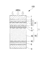
図1は、本発明の光電変換装置の構成を示す概略図である。光電変換装置100は、タンデム型シリコン系太陽電池であり、基板1、基板側透明電極層2、太陽電池光電変換層3としての第1電池層91(非晶質シリコン系)及び第2電池層92(結晶質シリコン系)、中間コンタクト層5、裏面側透明電極層6、及び裏面電極層4を備える。本実施形態において、基板側透明電極層2、中間コンタクト層5、及び、裏面側透明電極層6のうち少なくとも1つは、GaがドープされたZnO(GZO)膜とされる。
なお、上述のシリコン系とはシリコン(Si)やシリコンカーバイト(SiC)やシリコンゲルマニウム(SiGe)を含む総称である。また、結晶質シリコン系とは、非晶質シリコン系以外のシリコン系を意味するものであり、微結晶シリコンや多結晶シリコンも含まれる。
FIG. 1 is a schematic diagram illustrating a configuration of a photoelectric conversion device of the present invention. The
In addition, the above-mentioned silicon system is a general term including silicon (Si), silicon carbide (SiC), and silicon germanium (SiGe). Further, the crystalline silicon system means a silicon system other than the amorphous silicon system, and includes microcrystalline silicon and polycrystalline silicon.
<第1実施形態>
第1実施形態に係る光電変換装置の製造方法を、太陽電池パネルを製造する工程を例に挙げて説明する。図2から図5は、本実施形態の太陽電池パネルの製造方法を示す概略図である。
<First Embodiment>
A method for manufacturing a photoelectric conversion device according to the first embodiment will be described by taking a process for manufacturing a solar cell panel as an example. 2 to 5 are schematic views showing a method for manufacturing the solar cell panel of the present embodiment.
(1)図2(a)
基板1としてソーダフロートガラス基板(例えば面積が1m2以上、1.4m×1.1m×板厚:3.5mm〜4.5mm)を使用する。基板端面は熱応力や衝撃などによる破損防止にコーナー面取りやR面取り加工されていることが望ましい。
(1) FIG. 2 (a)
A soda float glass substrate (for example, an area of 1 m 2 or more, 1.4 m × 1.1 m × plate thickness: 3.5 mm to 4.5 mm) is used as the
(2)図2(b)
基板側透明電極層2として、DCマグネトロンスパッタリング装置により、膜厚400nm以上1000nm以下のGZO膜を形成する。製膜条件は、例えば、ターゲット:GaドープZnO焼結体、導入ガス:Arガス及びO2ガス、製膜圧力:0.2Pa、基板温度:120℃に設定する。基板側透明電極層として好適な導電性及び透明性を確保できれば、ターゲット中のGa(Ga2O3)ドープ量は任意の値に設定できる。上記条件の製膜により、透明電極膜の表面には、適当な凹凸のあるテクスチャーが形成される。
(2) FIG. 2 (b)
As the substrate-side
ここで、GZO製膜中のArガス分圧に対するN2ガス分圧の比をN2ガス分圧比としたときに、単位膜厚当たりのN2ガス分圧比が0.001%/nm以下となるように、基板側透明電極層2としてのGZO製膜時のN2ガス分圧比が制御される。単位膜厚当たりのN2ガス分圧比は、例えば、所定膜厚でのGZO膜の光吸収特性とN2ガス分圧比との関係を用い、可視光の短波長領域(例えば波長450〜600nm)での光吸収率から取得することができる。
Here, the ratio of N 2 gas partial pressure to the Ar gas partial pressure in the GZO film forming when the N 2 gas partial pressure ratio, N 2 gas partial pressure ratio per unit thickness is 0.001% / nm or less and Thus, the N 2 gas partial pressure ratio during GZO film formation as the substrate-side
GZO製膜中の単位膜厚当たりのN2ガス分圧比を上記範囲とする方法は、例えば、GZO製膜前の排気における到達圧力とN2ガス分圧比との関係を予め取得しておき、所望のN2ガス分圧比が得られる到達圧力に達するまで、チャンバの真空排気を実行するように製膜装置を制御する。また、N2ガスの主要な混入源は大気からのリークであることから、Heリークディテクタを用いてリーク源の特定を行い、Arガス流量に対して許容量以下のリークレートとすることにより、N2ガス分圧比を制御する。
GZO製膜中のArガス分圧及びN2ガス分圧をQ−massなどの質量分析計を用いて計測し、N2ガス分圧比が設定値を超えた場合に、製膜された基板側透明電極層は不良品として選別しても良い。
The method of setting the N 2 gas partial pressure ratio per unit film thickness in GZO film formation in the above range is, for example, acquiring in advance the relationship between the ultimate pressure in the exhaust before GZO film formation and the N 2 gas partial pressure ratio, The film forming apparatus is controlled to perform evacuation of the chamber until the ultimate pressure at which a desired N 2 gas partial pressure ratio is obtained is reached. In addition, since the main source of N 2 gas is leakage from the atmosphere, the leak source is specified using a He leak detector, and the leak rate is less than the allowable amount with respect to the Ar gas flow rate. The N 2 gas partial pressure ratio is controlled.
When the Ar gas partial pressure and N 2 gas partial pressure in GZO film formation are measured using a mass spectrometer such as Q-mass, and the N 2 gas partial pressure ratio exceeds a set value, the film-formed substrate side The transparent electrode layer may be selected as a defective product.
なお、中間コンタクト層5または裏面側透明電極層6としてGZO膜を形成する場合、基板側透明電極層2はGZO膜でなくても良い。例えば、基板側透明電極層2として、酸化錫(SnO2)を主成分とする膜厚500nm以上800nm以下の透明導電膜を、熱CVD装置にて約500℃で製膜する。
基板側透明電極層2として、透明電極膜に加えて、基板1と透明電極膜との間にアルカリバリア膜(図示されず)を形成しても良い。アルカリバリア膜は、酸化シリコン膜(SiO2)を50nm〜150nm、熱CVD装置にて約500℃で製膜処理する。
When a GZO film is formed as the
As the substrate-side
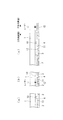
(3)図2(c)
その後、基板1をX−Yテーブルに設置して、YAGレーザーの第1高調波(1064nm)を、図の矢印に示すように、透明電極膜の膜面側から照射する。加工速度に適切となるようにレーザーパワーを調整して、透明電極膜を発電セルの直列接続方向に対して垂直な方向へ、基板1とレーザー光を相対移動して、溝10を形成するように幅約6mmから15mmの所定幅の短冊状にレーザーエッチングする。
(3) FIG. 2 (c)
Thereafter, the
(4)図2(d)
第1電池層91として、非晶質シリコン薄膜からなるp層、i層及びn層を、プラズマCVD装置により製膜する。SiH4ガス及びH2ガスを主原料にして、減圧雰囲気:30Pa以上1000Pa以下、基板温度:約200℃にて、基板側透明電極層2上に太陽光の入射する側から非晶質シリコンp層31、非晶質シリコンi層32、非晶質シリコンn層33の順で製膜する。非晶質シリコンp層31は非晶質のBドープシリコンを主とし、膜厚10nm以上30nm以下である。非晶質シリコンi層32は、膜厚200nm以上350nm以下である。非晶質シリコンn層33は、非晶質シリコンに微結晶シリコンを含有するPドープシリコンを主とし、膜厚30nm以上50nm以下である。非晶質シリコンp層31と非晶質シリコンi層32の間には、界面特性の向上のためにバッファー層を設けても良い。
(4) FIG. 2 (d)
As the
第1電池層91と第2電池層92の間に、接触性を改善するとともに電流整合性を取るために半反射膜となる中間コンタクト層5を設ける。中間コンタクト層5として、DCマグネトロンスパッタリング装置により、膜厚:20nm以上100nm以下のGZO膜を形成する。中間コンタクト層として好適な導電性及び透明性を確保できれば、ターゲット中のGaドープ量は任意の値に設定できる。製膜条件は、基板側透明電極層としてGZO膜を設ける場合と同様とされる。
An
中間コンタクト層の場合、製膜中の単位膜厚当たりのN2ガス分圧比は、0.025%/nm以下となるように制御される。GZO製膜中の単位膜厚当たりのN2ガス分圧比を上記範囲とする方法は、上述の基板側透明電極層2と同様の方法を採用できる。
中間コンタクト層製膜中のArガス分圧及びN2ガス分圧を質量分析計を用いて計測し、N2ガス分圧比が設定値を超えた場合に、製膜された中間コンタクト層は不良品として選別しても良い。
In the case of the intermediate contact layer, the N 2 gas partial pressure ratio per unit film thickness during film formation is controlled to be 0.025% / nm or less. As a method for setting the N 2 gas partial pressure ratio per unit film thickness in the GZO film formation within the above range, the same method as that for the substrate-side
When the Ar gas partial pressure and N 2 gas partial pressure in the intermediate contact layer deposition are measured using a mass spectrometer, and the N 2 gas partial pressure ratio exceeds the set value, the deposited intermediate contact layer is not It may be selected as a good product.
なお、基板側透明電極層2または裏面側透明電極層6としてGZO膜を形成する場合、中間コンタクト層5は、FドープされたSnO2、ITOなどの他の透明導電性酸化物とされても良い。また、中間コンタクト層5を設けない場合もある。
When forming a GZO film as the substrate-side
次に、第1電池層91の上に、プラズマCVD装置により、減圧雰囲気:3000Pa以下、基板温度:約200℃、プラズマ発生周波数:40MHz以上100MHz以下にて、第2電池層92としての結晶質シリコンp層41、結晶質シリコンi層42、及び、結晶質シリコンn層43を順次製膜する。結晶質シリコンp層41はBドープした微結晶シリコンを主とし、膜厚10nm以上50nm以下である。結晶質シリコンi層42は微結晶シリコンを主とし、膜厚は1.2μm以上3.0μm以下である。結晶質シリコンn層43はPドープした微結晶シリコンを主とし、膜厚20nm以上50nm以下である。
Next, a crystalline material as the
微結晶シリコンを主とするi層膜をプラズマCVD法で形成するにあたり、プラズマ放電電極と基板1の表面との距離dは、3mm以上10mm以下にすることが好ましい。3mmより小さい場合、大型基板に対応する製膜室内の各構成機器精度から距離dを一定に保つことが難しくなるとともに、近過ぎて放電が不安定になる恐れがある。10mmより大きい場合、十分な製膜速度(1nm/s以上)を得難くなるとともに、プラズマの均一性が低下しイオン衝撃により膜質が低下する。
In forming the i-layer film mainly composed of microcrystalline silicon by the plasma CVD method, the distance d between the plasma discharge electrode and the surface of the
(5)図2(e)
基板1をX−Yテーブルに設置して、レーザーダイオード励起YAGレーザーの第2高調波(532nm)を、図の矢印に示すように、光電変換層3の膜面側から照射する。パルス発振:10kHzから20kHzとして、加工速度に適切となるようにレーザーパワーを調整して、基板側透明電極層2のレーザーエッチングラインの約100μmから150μmの横側を、溝11を形成するようにレーザーエッチングする。またこのレーザーは基板1側から照射しても良く、この場合は光電変換層3の非晶質シリコン系の第1電池層で吸収されたエネルギーで発生する高い蒸気圧を利用して光電変換層3をエッチングできるので、更に安定したレーザーエッチング加工を行うことが可能となる。レーザーエッチングラインの位置は前工程でのエッチングラインと交差しないように位置決め公差を考慮して選定する。
(5) FIG. 2 (e)
The
(6)図3(a)
結晶質シリコンn層43と裏面電極層4との接触抵抗低減と光反射向上を目的として、光電変換層3と裏面電極層4との間に裏面側透明電極層6が設けられる。裏面側透明電極層6として、DCマグネトロンスパッタリング装置により、膜厚:50nm以上100nm以下のGZO膜を形成する。この場合も、裏面側透明電極層として好適な導電性及び透明性を確保できれば、ターゲット中のGaドープ量は任意の値に設定できる。製膜条件は、基板側透明電極層としてGZO膜を設ける場合と同様とされる。
(6) FIG. 3 (a)
For the purpose of reducing the contact resistance between the crystalline
中間コンタクト層5と同様に、単位膜厚当たりのN2ガス分圧比が0.025%/nm以下となるように、裏面側透明電極層6としてのGZO製膜時におけるN2ガス分圧比が制御される。GZO製膜中の単位膜厚当たりのN2ガス分圧比を上記範囲とする方法は、上述の基板側透明電極層2と同様の方法を採用できる。また、GZO製膜中のArガス分圧及びN2ガス分圧を質量分析計を用いて計測し、N2ガス分圧比が設定値を超えた場合に、製膜された裏面側透明電極層は不良品として選別しても良い。
Like the
基板側透明電極層2または中間コンタクト層5としてGZO膜を形成する場合、裏面側透明電極層6は、他の透明導電性酸化物とされても良い。また、基板側透明電極層6を設けない場合もある。
When a GZO film is formed as the substrate side
裏面電極層4としてAg膜/Ti膜を、スパッタリング装置により、減圧雰囲気、製膜温度:150℃から200℃にて製膜する。本実施形態では、Ag膜:150nm以上500nm以下、これを保護するものとして防食効果の高いTi膜:10nm以上20nm以下を、この順に積層する。あるいは、裏面電極層4を、25nmから100nmの膜厚を有するAg膜と、15nmから500nmの膜厚を有するAl膜との積層構造としても良い。
An Ag film / Ti film is formed as the
(7)図3(b)
基板1をX−Yテーブルに設置して、レーザーダイオード励起YAGレーザーの第2高調波(532nm)を、図の矢印に示すように、基板1側から照射する。レーザー光が光電変換層3で吸収され、このとき発生する高いガス蒸気圧を利用して裏面電極層4が爆裂して除去される。パルス発振:1kHz以上10kHz以下として加工速度に適切となるようにレーザーパワーを調整して、基板側透明電極層2のレーザーエッチングラインの250μmから400μmの横側を、溝12を形成するようにレーザーエッチングする。
(7) FIG. 3 (b)
The
(8)図3(c)と図4(a)
発電領域を区分して、基板端周辺の膜端部をレーザーエッチングし、直列接続部分で短絡し易い影響を除去する。基板1をX−Yテーブルに設置して、レーザーダイオード励起YAGレーザーの第2高調波(532nm)を、基板1側から照射する。レーザー光が基板側透明電極層2と光電変換層3で吸収され、このとき発生する高いガス蒸気圧を利用して裏面電極層4が爆裂して、裏面電極層4/光電変換層3/基板側透明電極層2が除去される。パルス発振:1kHz以上10kHz以下として加工速度に適切となるようにレーザーパワーを調整して、基板1の端部から5mmから20mmの位置を、図3(c)に示すように、X方向絶縁溝15を形成するようにレーザーエッチングする。なお、図3(c)では、光電変換層3が直列に接続された方向に切断したX方向断面図となっているため、本来であれば絶縁溝15位置には裏面電極層4/光電変換層3/基板側透明電極層2の膜研磨除去をした周囲膜除去領域14がある状態(図4(a)参照)が表れるべきであるが、基板1の端部への加工の説明の便宜上、この位置にY方向断面を表して形成された絶縁溝をX方向絶縁溝15として説明する。このとき、Y方向絶縁溝は後工程で基板1周囲膜除去領域の膜面研磨除去処理を行うので、設ける必要がない。
(8) FIG. 3 (c) and FIG. 4 (a)
The power generation region is divided, and the film edge around the substrate edge is laser-etched to eliminate the effect of short circuit at the serial connection portion. The
絶縁溝15は基板1の端より5mmから15mmの位置にてエッチングを終了させることにより、太陽電池パネル端部からの太陽電池モジュール7内部への外部湿分浸入の抑制に、有効な効果を呈するので好ましい。
The insulating
尚、以上までの工程におけるレーザー光はYAGレーザーとしているが、YVO4レーザーやファイバーレーザーなどが同様に使用できるものがある。 In addition, although the laser beam in the above process is made into a YAG laser, there exists what can use a YVO4 laser, a fiber laser, etc. similarly.
(9)図4(a:太陽電池膜面側から見た図、b:受光面の基板側から見た図)
後工程のEVA等を介したバックシート24との健全な接着・シール面を確保するために、基板1周辺(周囲膜除去領域14)の積層膜は、段差があるとともに剥離し易いため、この膜を除去して周囲膜除去領域14を形成する。基板1の端から5〜20mmで基板1の全周囲にわたり膜を除去するにあたり、X方向は前述の図3(c)工程で設けた絶縁溝15よりも基板端側において、Y方向は基板端側部付近の溝10よりも基板端側において、裏面電極層4/光電変換層3/基板側透明電極層2を、砥石研磨やブラスト研磨などを用いて除去を行う。
研磨屑や砥粒は基板1を洗浄処理して除去した。
(9) FIG. 4 (a: view from the solar cell film side, b: view from the substrate side of the light receiving surface)
Since the laminated film around the substrate 1 (peripheral film removal region 14) has a step and is easy to peel off in order to ensure a sound adhesion / seal surface with the
Polishing debris and abrasive grains were removed by cleaning the
(10)図5(a)(b)
端子箱23の取付け部分はバックシート24に開口貫通窓を設けて集電板を取出す。この開口貫通窓部分には絶縁材を複数層で設置して外部からの湿分などの浸入を抑制する。
直列に並んだ一方端の太陽電池発電セルと、他方端部の太陽電池発電セルとから銅箔を用いて集電して太陽電池パネル裏側の端子箱23の部分から電力が取出せるように処理する。銅箔は各部との短絡を防止するために銅箔幅より広い絶縁シートを配置する。
集電用銅箔などが所定位置に配置された後に、太陽電池モジュール7の全体を覆い、基板1からはみ出さないようにEVA(エチレン酢酸ビニル共重合体)等による接着充填材シートを配置する。
EVAの上に、防水効果の高いバックシート24を設置する。バックシート24は本実施形態では防水防湿効果が高いようにPETシート/Al箔/PETシートの3層構造よりなる。
バックシート24までを所定位置に配置したものを、ラミネータにより減圧雰囲気で内部の脱気を行い約150〜160℃でプレスしながら、EVAを架橋させて密着させる。
(10) FIGS. 5 (a) and 5 (b)
An attachment portion of the
Processing so that power can be taken out from the
After the collector copper foil and the like are arranged at a predetermined position, an adhesive filler sheet made of EVA (ethylene vinyl acetate copolymer) or the like is arranged so as to cover the entire solar cell module 7 and not to protrude from the
A
The EVA sheet is placed in a predetermined position until the
(11)図5(a)
太陽電池モジュール7の裏側に端子箱23を接着剤で取付ける。
(12)図5(b)
銅箔と端子箱23の出力ケーブルとをハンダ等で接続し、端子箱23の内部を封止剤(ポッティング剤)で充填して密閉する。これで太陽電池パネル50が完成する。
(13)図5(c)
図5(b)までの工程で形成された太陽電池パネル50について発電検査ならびに、所定の性能試験を行う。発電検査は、AM1.5、全天日射基準太陽光(1000W/m2)のソーラシミュレータを用いて行う。
(14)図5(d)
発電検査(図5(c))に前後して、外観検査をはじめ所定の性能検査を行う。
(11) FIG. 5 (a)
The
(12) FIG. 5 (b)
The copper foil and the output cable of the
(13) FIG. 5 (c)
A power generation inspection and a predetermined performance test are performed on the
(14) FIG. 5 (d)
Before and after the power generation inspection (FIG. 5C), a predetermined performance inspection is performed including an appearance inspection.
上記実施の形態では太陽電池として、タンデム型太陽電池について説明したが、本発明は、この例に限定されるものではない。例えば、非晶質シリコン太陽電池、微結晶シリコンをはじめとする結晶質シリコン太陽電池、シリコンゲルマニウム太陽電池、トリプル型太陽電池などの他の種類の薄膜太陽電池にも同様に適用可能である。 Although the tandem solar cell has been described as the solar cell in the above embodiment, the present invention is not limited to this example. For example, the present invention can be similarly applied to other types of thin film solar cells such as amorphous silicon solar cells, crystalline silicon solar cells including microcrystalline silicon, silicon germanium solar cells, and triple solar cells.
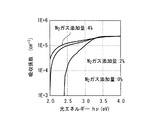
<ドーパント組成によるGZO膜の光吸収率>
5.7wt%Ga2O3−ZnOターゲットまたは0.5wt%Ga2O3−ZnOターゲットを用い、DCマグネトロンスパッタリング装置によりガラス基板上にGZO膜を製膜した。製膜条件は、製膜前の到達圧力:1×10⁻⁴Pa以下、製膜ガス:Arガス、O2ガス(0.15sccm)、N2ガス、Arガス量に対するN2ガス添加量(N2ガス分圧比):0〜4%、製膜圧力:0.2Pa、基板温度:120℃、ターゲット−基板間距離:90mm、目標膜厚:80nmとした。なお、N2ガス分圧比は、Arガス流量及びN2ガス流量から求めた値とした。
<Light absorption rate of GZO film by dopant composition>
A GZO film was formed on a glass substrate by a DC magnetron sputtering apparatus using a 5.7 wt% Ga 2 O 3 —ZnO target or a 0.5 wt% Ga 2 O 3 —ZnO target. The film forming conditions are: ultimate pressure before film forming: 1 × 10 −4 Pa or less, film forming gas: Ar gas, O 2 gas (0.15 sccm), N 2 gas, N 2 gas addition amount with respect to Ar gas amount ( N 2 gas partial pressure ratio): 0 to 4%, film forming pressure: 0.2 Pa, substrate temperature: 120 ° C., target-substrate distance: 90 mm, target film thickness: 80 nm. The N 2 gas partial pressure ratio was a value obtained from the Ar gas flow rate and the N 2 gas flow rate.
波長300〜1200nmでの各GZO膜の透過率及び反射率を測定し、光吸収率を100−透過率−反射率(%)として算出した。図6及び図7に、Ga2O3ドープ量がそれぞれ5.7wt%、0.5wt%であるGZO膜の光吸収スペクトルを示す。同図において、横軸は波長、縦軸は光吸収率である。
図6及び図7の光吸収スペクトルを、光子エネルギー及び吸収係数で表したものを図8及び図9に示す。同図において、横軸は光子エネルギー、縦軸は吸収係数である。
波長400nm以下の領域では、Ga2O3含有量の増加によるGZO吸収端が短波長側にシフトする。波長450nm(2.76eV)〜600nm(2.07eV)では、N2分圧比が高くなるのにも伴い、Ga2O3添加量が10倍異なるにも拘らずほぼ同等の光吸収率及び吸収係数が得られた。これは、450〜600nmの波長域の吸収は、GZO膜に窒素が取り込まれたために生じることを示している。
The transmittance and reflectance of each GZO film at a wavelength of 300 to 1200 nm were measured, and the light absorption rate was calculated as 100−transmittance−reflectance (%). 6 and 7 show light absorption spectra of the GZO film having Ga 2 O 3 doping amounts of 5.7 wt% and 0.5 wt%, respectively. In the figure, the horizontal axis represents wavelength and the vertical axis represents light absorption.
FIGS. 8 and 9 show the light absorption spectra of FIGS. 6 and 7 in terms of photon energy and absorption coefficient. In the figure, the horizontal axis represents photon energy and the vertical axis represents the absorption coefficient.
In the region of
<GZO製膜時のN2分圧比と太陽電池性能との関係>
(裏面側透明電極層)
裏面側透明電極層としてのGZO膜製膜時のN2分圧比を変えたシングル型非晶質シリコン太陽電池セルの電池性能を評価した。
大きさが1.4m×1.1mのガラス基板を用いて、以下の層構成を有するシングル型非晶質シリコン太陽電池セルを作製した。裏面側透明電極層としてのGZO膜の製膜では、Arガスに対するN2ガス添加量(N2ガス分圧比)を0%、1%、2%、4%、8%とした。その他の製膜条件は、上述のGZO膜の光吸収係数を確認した試験と同一とした。
基板側透明電極層:SnO2膜、平均膜厚400nm
非晶質シリコンp層:膜厚100nm
非晶質シリコンi層:膜厚200nm
結晶質シリコンn層:膜厚30nm
裏面側透明電極層:GZO膜(Ga2O30.5wt%)、膜厚80nm
裏面電極層:Ag膜、膜厚250nm
<Relationship between N 2 partial pressure ratio and solar cell performance during GZO film formation>
(Back side transparent electrode layer)
The battery performance of the single-type amorphous silicon solar battery cell in which the N 2 partial pressure ratio at the time of forming the GZO film as the back side transparent electrode layer was changed was evaluated.
Using a glass substrate having a size of 1.4 m × 1.1 m, a single-type amorphous silicon solar battery cell having the following layer structure was manufactured. In the formation of the GZO film as the back side transparent electrode layer, the amount of N 2 gas added to the Ar gas (N 2 gas partial pressure ratio) was set to 0%, 1%, 2%, 4%, and 8%. The other film forming conditions were the same as the above-described test for confirming the light absorption coefficient of the GZO film.
Substrate side transparent electrode layer: SnO 2 film,
Amorphous silicon p layer: film thickness 100nm
Amorphous silicon i layer: 200 nm thickness
Crystalline silicon n layer: film thickness 30nm
Back side transparent electrode layer: GZO film (Ga 2 O 3 0.5 wt%),
Back electrode layer: Ag film, film thickness 250 nm
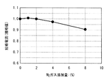
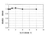
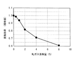
図10乃至図13に、裏面側透明電極層としてGZO膜を形成したシングル型太陽電池セルの電池特性と、GZO製膜時のN2ガス添加量との関係を示す。同図において、横軸はN2ガス添加量である。縦軸は、図10では短絡電流、図11では開放電圧、図12では形状因子、図13では光電変換効率であり、それぞれN2ガス添加量0%のときの値を1として規格化した。
GZO膜製膜時のN2ガス添加量が増加するに従い、短絡電流及び光電変換効率は減少した。一方、開放電圧及び形状因子はN2ガス添加量に依存しなかった。GZO膜への窒素混入による太陽電池セル光電変換効率の低下は、5%まで許容できる。従って、裏面側透明電極層としてGZO膜を製膜した場合、N2ガス添加量は2%以下に管理する必要がある。
図6及び図7を参照すると、GZO膜厚80nm及びN2ガス添加量2%以下の場合、波長450〜600nmの領域ではドーパント量に依らず光吸収率20%以下が確実に達成できる。このようなGZO膜の光吸収率とN2ガス添加量との関係を用いれば、GZO膜の光吸収率から好適なN2ガス添加量(N2ガス分圧比)を取得することができる。
FIG. 10 to FIG. 13 show the relationship between the battery characteristics of a single solar cell in which a GZO film is formed as the back side transparent electrode layer and the amount of N 2 gas added during GZO film formation. In the figure, the horizontal axis represents the amount of N 2 gas added. The vertical axis represents the 10 in the short-circuit current,
As the amount of N 2 gas added during GZO film formation increased, the short-circuit current and photoelectric conversion efficiency decreased. On the other hand, the open circuit voltage and the shape factor did not depend on the N 2 gas addition amount. A decrease in the photovoltaic cell photoelectric conversion efficiency due to nitrogen mixing in the GZO film is acceptable up to 5%. Therefore, when a GZO film is formed as the back side transparent electrode layer, the N 2 gas addition amount needs to be controlled to 2% or less.
Referring to FIGS. 6 and 7, when the GZO film thickness is 80 nm and the N 2 gas addition amount is 2% or less, the light absorption rate of 20% or less can be reliably achieved in the wavelength region of 450 to 600 nm regardless of the dopant amount. Using such a relationship between the light absorption rate of the GZO film and the N 2 gas addition amount, a suitable N 2 gas addition amount (N 2 gas partial pressure ratio) can be obtained from the light absorption rate of the GZO film.
ここで、窒素を含有するGZO膜での光学的損失Aは式(1)で表される。
A=I0×{1−exp(−αd)} …(1)
(I0:入射光強度、α:吸収係数、d:GZO膜厚)
αd≦0.2、すなわち、光吸収率20%以下では、1−exp(−αd)≒αdとなるため、光学的損失Aは式(2)で表される。
A≒I0×αd …(2)
光学的損失分の短絡電流が減少することから、短絡電流の減少量はGZOの膜厚に比例する。従って、裏面側透明電極層としてGZO膜を製膜する場合、単位膜厚当たりのN2ガス分圧比は、2%/80nm=0.025%/nm以下とする。
なお、裏面側透明電極層の膜厚が50nmから100nmで同様の実験を行ったところ、N2ガス分圧比0.025%/nm以下で、短絡電流及び光電変換効率の低下を抑制することが確認できた。
Here, the optical loss A in the GZO film containing nitrogen is expressed by the formula (1).
A = I 0 × {1-exp (−αd)} (1)
(I 0 : incident light intensity, α: absorption coefficient, d: GZO film thickness)
When αd ≦ 0.2, that is, when the optical absorptance is 20% or less, 1−exp (−αd) ≈αd, and thus the optical loss A is expressed by the equation (2).
A≈I 0 × αd (2)
Since the short-circuit current corresponding to the optical loss decreases, the amount of decrease in the short-circuit current is proportional to the thickness of the GZO film. Therefore, when a GZO film is formed as the back side transparent electrode layer, the N 2 gas partial pressure ratio per unit film thickness is 2% / 80 nm = 0.025% / nm or less.
In addition, when the same experiment was performed when the film thickness of the back surface side transparent electrode layer was 50 nm to 100 nm, the N 2 gas partial pressure ratio was 0.025% / nm or less to suppress the short circuit current and the decrease in photoelectric conversion efficiency. It could be confirmed.
(中間コンタクト層)
中間コンタクト層としてのGZO膜製膜時のN2分圧比を変えたタンデム型シリコン太陽電池セルの電池性能を評価した。
大きさが1.4m×1.1mのガラス基板を用いて、タンデム型シリコン太陽電池セルの層構成を以下に示す。中間コンタクト層としてのGZO膜の製膜では、Arガスに対するN2ガス添加量(N2ガス分圧比)を0%、1%、2%、4%、8%とした。その他のGZO製膜条件は、上述のGZO膜の光吸収係数を確認した試験と同一とした。
基板側透明電極層:SnO2膜、平均膜厚400nm
非晶質シリコンp層:膜厚10nm
非晶質シリコンi層:膜厚200nm
結晶質シリコンn層:膜厚30nm
中間コンタクト層:GZO膜(Ga2O30.5wt%)、膜厚80nm
結晶質シリコンp層:膜厚20nm
結晶質シリコンi層:膜厚2000nm
結晶質シリコンn層:膜厚30nm
裏面側透明電極層:GZO膜(Ga2O30.5wt%、N2ガス添加量0%)、膜厚80nm
裏面電極層:Ag、膜厚250nm
(Intermediate contact layer)
The battery performance of the tandem type silicon solar cell in which the N 2 partial pressure ratio at the time of forming the GZO film as the intermediate contact layer was changed was evaluated.
The layer structure of the tandem silicon solar battery cell is shown below using a glass substrate having a size of 1.4 m × 1.1 m. In the formation of the GZO film as the intermediate contact layer, the amount of N 2 gas added to the Ar gas (N 2 gas partial pressure ratio) was set to 0%, 1%, 2%, 4%, and 8%. The other GZO film forming conditions were the same as those in the test for confirming the light absorption coefficient of the GZO film.
Substrate side transparent electrode layer: SnO 2 film,
Amorphous silicon p layer: film thickness 10nm
Amorphous silicon i layer: 200 nm thickness
Crystalline silicon n layer: film thickness 30nm
Intermediate contact layer: GZO film (Ga 2 O 3 0.5 wt%),
Crystalline silicon p layer: film thickness 20nm
Crystalline silicon i layer: film thickness 2000nm
Crystalline silicon n layer: film thickness 30nm
Back side transparent electrode layer: GZO film (Ga 2 O 3 0.5 wt%, N 2
Back electrode layer: Ag, film thickness 250 nm
図14乃至図17に、基板側透明電極層としてGZO膜を形成したタンデム型太陽電池セルの電池特性と、GZO製膜時のN2ガス添加量との関係を示す。同図において、横軸はN2ガス添加量である。縦軸は、図14では短絡電流、図15では開放電圧、図16では形状因子、図17では光電変換効率であり、それぞれN2ガス添加量0%のときの値を1として規格化した。
GZO膜製膜時のN2ガス添加量が増加するに従い、短絡電流及び光電変換効率は減少した。一方、開放電圧及び形状因子はN2ガス添加量に依存しなかった。GZO膜への窒素混入による太陽電池セル光電変換効率の低下は、5%まで許容できる。従って、中間コンタクト層としてGZO膜を製膜した場合、N2ガス添加量は2%以下に管理する必要がある。
上述のように、短絡電流は窒素を含有するGZOの膜厚に比例することから、中間コンタクト層としてGZO膜を製膜する場合、単位膜厚当たりのN2ガス分圧比は、0.025%/nm以下とする。
なお、中間コンタクト層の膜厚が20nmから100nmにおいても、N2ガス分圧比0.025%/nm以下で、短絡電流及び光電変換効率の低下を抑制することが確認できた。
14 to 17 show the relationship between the battery characteristics of a tandem solar cell in which a GZO film is formed as a substrate-side transparent electrode layer and the amount of N 2 gas added during GZO film formation. In the figure, the horizontal axis represents the amount of N 2 gas added. The vertical axis represents the short-circuit current in FIG. 14, the open circuit voltage in FIG. 15, the form factor in FIG. 16, the photoelectric conversion efficiency in FIG. 17, and the values when the N 2 gas addition amount is 0% are each normalized as 1.
As the amount of N 2 gas added during GZO film formation increased, the short-circuit current and photoelectric conversion efficiency decreased. On the other hand, the open circuit voltage and the shape factor did not depend on the N 2 gas addition amount. A decrease in the photovoltaic cell photoelectric conversion efficiency due to nitrogen mixing in the GZO film is acceptable up to 5%. Therefore, when a GZO film is formed as the intermediate contact layer, the N 2 gas addition amount needs to be controlled to 2% or less.
As described above, since the short-circuit current is proportional to the thickness of GZO containing nitrogen, when a GZO film is formed as an intermediate contact layer, the N 2 gas partial pressure ratio per unit thickness is 0.025%. / Nm or less.
In addition, even when the film thickness of the intermediate contact layer was 20 nm to 100 nm, it was confirmed that the N 2 gas partial pressure ratio was 0.025% / nm or less to suppress the short circuit current and the decrease in photoelectric conversion efficiency.
(基板側透明電極層)
基板側透明電極層としてのGZO膜製膜時のN2分圧比を変えたシングル型結晶質シリコン太陽電池セルの電池性能を評価した。
大きさが1.4m×1.1mのガラス基板を用いて、以下の層構成を有するシングル型結晶質シリコン太陽電池セルを作製した。
基板側透明電極層:GZO膜(Ga2O30.5wt%)、平均膜厚400nm
結晶質シリコンp層:膜厚20nm
結晶質シリコンi層:膜厚2000nm
結晶質シリコンn層:膜厚30nm
裏面側透明電極層:GZO膜(Ga2O30.5wt%、N2ガス添加量0%)、膜厚80nm
裏面電極層:Ag膜、膜厚250nm
基板側透明電極層としてのGZO膜の製膜では、Arガスに対するN2ガス添加量(N2ガス分圧比)を0%、0.4%、1%、2%、4%、8%とした。その他のGZO製膜条件は、上述のGZO膜の光吸収係数を確認した試験と同一とした。
(Substrate side transparent electrode layer)
The battery performance of the single-type crystalline silicon solar cell in which the N 2 partial pressure ratio at the time of forming the GZO film as the substrate-side transparent electrode layer was changed was evaluated.
Using a glass substrate having a size of 1.4 m × 1.1 m, a single-type crystalline silicon solar battery cell having the following layer structure was produced.
Substrate side transparent electrode layer: GZO film (Ga 2 O 3 0.5 wt%),
Crystalline silicon p layer: film thickness 20nm
Crystalline silicon i layer: film thickness 2000nm
Crystalline silicon n layer: film thickness 30nm
Back side transparent electrode layer: GZO film (Ga 2 O 3 0.5 wt%, N 2
Back electrode layer: Ag film, film thickness 250 nm
In the formation of the GZO film as the substrate-side transparent electrode layer, the amount of N 2 gas added to the Ar gas (N 2 gas partial pressure ratio) is 0%, 0.4%, 1%, 2%, 4%, and 8%. did. The other GZO film forming conditions were the same as those in the test for confirming the light absorption coefficient of the GZO film.
図18乃至図21に、基板側透明電極層としてGZO膜を形成したシングル型太陽電池セルの電池特性と、GZO製膜時のN2ガス添加量との関係を示す。同図において、横軸はN2ガス添加量である。縦軸は、図18では短絡電流、図19では開放電圧、図20では形状因子、図21では光電変換効率であり、それぞれN2ガス添加量0%のときの値を1として規格化した。
GZO膜製膜時のN2ガス添加量が増加するに従い、短絡電流及び光電変換効率は減少した。一方、開放電圧及び形状因子はN2ガス添加量に依存しなかった。GZO膜への窒素混入による太陽電池セル光電変換効率の低下は、5%まで許容できる。そのため、基板側透明電極層としてGZO膜を製膜した場合、N2ガス添加量は0.4%以下に管理する必要がある。すなわち、基板側透明電極層としてGZO膜を製膜する場合、単位膜厚当たりのN2ガス分圧比は、0.4%/400nm=0.001%/nm以下とする。基板側透明電極層は光電変換層に対して光入射側にあり厚膜とされるため、基板側透明電極層の場合は、中間コンタクト層や裏面側透明電極層の場合よりもGZO膜の光吸収率を小さくすることが必要である。太陽電池中でGZO膜が配置される位置に応じて、要求されるGZO膜の光吸収率を適宜設定し、N2分圧比を決定すると良い。
なお、基板側透明電極層の膜厚が400nmから1000nmにおいても、N2ガス分圧比0.001%/nm以下で、短絡電流及び光電変換効率の低下を抑制することが確認できた。
FIG. 18 to FIG. 21 show the relationship between the battery characteristics of a single solar cell in which a GZO film is formed as the substrate-side transparent electrode layer, and the amount of N 2 gas added during GZO film formation. In the figure, the horizontal axis represents the amount of N 2 gas added. The vertical axis represents the short-circuit current in FIG. 18, the open circuit voltage in FIG. 19, the form factor in FIG. 20, the photoelectric conversion efficiency in FIG. 21, and the value when the N 2 gas addition amount is 0% is normalized as 1.
As the amount of N 2 gas added during GZO film formation increased, the short-circuit current and photoelectric conversion efficiency decreased. On the other hand, the open circuit voltage and the shape factor did not depend on the N 2 gas addition amount. A decrease in the photovoltaic cell photoelectric conversion efficiency due to nitrogen mixing in the GZO film is acceptable up to 5%. Therefore, when a GZO film is formed as the substrate-side transparent electrode layer, the N 2 gas addition amount needs to be controlled to 0.4% or less. That is, when a GZO film is formed as the substrate-side transparent electrode layer, the N 2 gas partial pressure ratio per unit film thickness is 0.4% / 400 nm = 0.001% / nm or less. Since the substrate side transparent electrode layer is on the light incident side with respect to the photoelectric conversion layer and is a thick film, in the case of the substrate side transparent electrode layer, the light of the GZO film is lighter than in the case of the intermediate contact layer or the back surface side transparent electrode layer. It is necessary to reduce the absorption rate. Depending on the position where the GZO film is disposed in the solar cell, the required light absorption rate of the GZO film may be set as appropriate to determine the N 2 partial pressure ratio.
In addition, even if the film thickness of the substrate side transparent electrode layer was 400 nm to 1000 nm, it was confirmed that the N 2 gas partial pressure ratio was 0.001% / nm or less and the short circuit current and the decrease in photoelectric conversion efficiency were suppressed.
1 基板
2 基板側透明電極層
3 光電変換層
4 裏面電極層
5 中間コンタクト層
6 裏面側透明電極層
7 太陽電池モジュール
31 非晶質シリコンp層
32 非晶質シリコンi層
33 非晶質シリコンn層
41 結晶質シリコンp層
42 結晶質シリコンi層
43 結晶質シリコンn層
91 第1電池層
92 第2電池層
100 光電変換装置
DESCRIPTION OF
Claims (3)
前記基板側透明電極層、前記中間コンタクト層、及び前記裏面側透明電極層として、GaがドープされたZnOを主とする透明導電膜を、該透明導電膜の単位膜厚当たりの不活性ガス分圧に対するN2ガス分圧の比が所定値以下となるように、前記N2ガス分圧を制御して製膜する光電変換装置の製造方法。 At least one of a step of forming a substrate-side transparent electrode layer on the substrate, a step of forming an intermediate contact layer between two adjacent battery layers, and a step of forming a back-side transparent electrode layer on the photoelectric conversion layer One process is
As the substrate-side transparent electrode layer, the intermediate contact layer, and the back-side transparent electrode layer, a transparent conductive film mainly containing ZnO doped with Ga is used as an inert gas component per unit film thickness of the transparent conductive film. A method for manufacturing a photoelectric conversion device, in which a film is formed by controlling the N 2 gas partial pressure so that a ratio of the N 2 gas partial pressure to the pressure is a predetermined value or less.
Priority Applications (5)
| Application Number | Priority Date | Filing Date | Title |
|---|---|---|---|
| JP2009209293A JP2011061017A (en) | 2009-09-10 | 2009-09-10 | Method of manufacturing photoelectric converter |
| EP10815196A EP2477233A1 (en) | 2009-09-10 | 2010-06-23 | Production method for photovoltaic device |
| PCT/JP2010/060599 WO2011030598A1 (en) | 2009-09-10 | 2010-06-23 | Production method for photovoltaic device |
| CN2010800185065A CN102414842A (en) | 2009-09-10 | 2010-06-23 | Production method for photovoltaic device |
| US13/264,277 US20120040494A1 (en) | 2009-09-10 | 2010-06-23 | Process for producing photovoltaic device |
Applications Claiming Priority (1)
| Application Number | Priority Date | Filing Date | Title |
|---|---|---|---|
| JP2009209293A JP2011061017A (en) | 2009-09-10 | 2009-09-10 | Method of manufacturing photoelectric converter |
Publications (2)
| Publication Number | Publication Date |
|---|---|
| JP2011061017A true JP2011061017A (en) | 2011-03-24 |
| JP2011061017A5 JP2011061017A5 (en) | 2011-11-24 |
Family
ID=43732275
Family Applications (1)
| Application Number | Title | Priority Date | Filing Date |
|---|---|---|---|
| JP2009209293A Pending JP2011061017A (en) | 2009-09-10 | 2009-09-10 | Method of manufacturing photoelectric converter |
Country Status (5)
| Country | Link |
|---|---|
| US (1) | US20120040494A1 (en) |
| EP (1) | EP2477233A1 (en) |
| JP (1) | JP2011061017A (en) |
| CN (1) | CN102414842A (en) |
| WO (1) | WO2011030598A1 (en) |
Families Citing this family (4)
| Publication number | Priority date | Publication date | Assignee | Title |
|---|---|---|---|---|
| US20140203322A1 (en) * | 2013-01-23 | 2014-07-24 | Epistar Corporation | Transparent Conductive Structure, Device comprising the same, and the Manufacturing Method thereof |
| CN105051912B (en) * | 2013-03-15 | 2017-07-25 | 阿科玛股份有限公司 | Nitrogenous transparent conductive oxide cap rock composition |
| US9818903B2 (en) * | 2014-04-30 | 2017-11-14 | Sunpower Corporation | Bonds for solar cell metallization |
| US9577045B2 (en) | 2014-08-04 | 2017-02-21 | Fairchild Semiconductor Corporation | Silicon carbide power bipolar devices with deep acceptor doping |
Citations (3)
| Publication number | Priority date | Publication date | Assignee | Title |
|---|---|---|---|---|
| JP2007258537A (en) * | 2006-03-24 | 2007-10-04 | Mitsubishi Heavy Ind Ltd | Photoelectric conversion device and its manufacturing method |
| JP2009057605A (en) * | 2007-08-31 | 2009-03-19 | Hitachi Ltd | Zinc oxide thin film, transparent conductive film using it, and indicating element |
| JP2009135220A (en) * | 2007-11-29 | 2009-06-18 | Mitsubishi Heavy Ind Ltd | Manufacturing method for photoelectric conversion device |
Family Cites Families (3)
| Publication number | Priority date | Publication date | Assignee | Title |
|---|---|---|---|---|
| JP2908617B2 (en) | 1991-09-24 | 1999-06-21 | キヤノン株式会社 | Solar cell |
| US20050056863A1 (en) * | 2003-09-17 | 2005-03-17 | Matsushita Electric Industrial Co., Ltd. | Semiconductor film, method for manufacturing the semiconductor film, solar cell using the semiconductor film and method for manufacturing the solar cell |
| US20100155738A1 (en) * | 2005-02-22 | 2010-06-24 | Hiroyuki Nabeta | Light Emitting Diode and Method for Manufacturing Same |
-
2009
- 2009-09-10 JP JP2009209293A patent/JP2011061017A/en active Pending
-
2010
- 2010-06-23 CN CN2010800185065A patent/CN102414842A/en active Pending
- 2010-06-23 WO PCT/JP2010/060599 patent/WO2011030598A1/en active Application Filing
- 2010-06-23 EP EP10815196A patent/EP2477233A1/en not_active Withdrawn
- 2010-06-23 US US13/264,277 patent/US20120040494A1/en not_active Abandoned
Patent Citations (3)
| Publication number | Priority date | Publication date | Assignee | Title |
|---|---|---|---|---|
| JP2007258537A (en) * | 2006-03-24 | 2007-10-04 | Mitsubishi Heavy Ind Ltd | Photoelectric conversion device and its manufacturing method |
| JP2009057605A (en) * | 2007-08-31 | 2009-03-19 | Hitachi Ltd | Zinc oxide thin film, transparent conductive film using it, and indicating element |
| JP2009135220A (en) * | 2007-11-29 | 2009-06-18 | Mitsubishi Heavy Ind Ltd | Manufacturing method for photoelectric conversion device |
Also Published As
| Publication number | Publication date |
|---|---|
| WO2011030598A1 (en) | 2011-03-17 |
| EP2477233A1 (en) | 2012-07-18 |
| CN102414842A (en) | 2012-04-11 |
| US20120040494A1 (en) | 2012-02-16 |
Similar Documents
| Publication | Publication Date | Title |
|---|---|---|
| US20100116331A1 (en) | Photovoltaic device and process for producing same | |
| JP5022341B2 (en) | Photoelectric conversion device | |
| JP2009246029A (en) | Photoelectric conversion device | |
| WO2010052953A1 (en) | Photoelectric conversion device manufacturing method and photoelectric conversion device | |
| WO2011030598A1 (en) | Production method for photovoltaic device | |
| JP4764469B2 (en) | Photoelectric conversion device and method of manufacturing photoelectric conversion device | |
| US20100229935A1 (en) | Photovoltaic device | |
| WO2011061956A1 (en) | Photoelectric conversion device | |
| WO2011070805A1 (en) | Process for production of photoelectric conversion device | |
| JP5254917B2 (en) | Method for manufacturing photoelectric conversion device | |
| JP5030745B2 (en) | Method for manufacturing photoelectric conversion device | |
| WO2010064455A1 (en) | Photoelectric conversion device | |
| WO2012014550A1 (en) | Method for production of photoelectric conversion device | |
| WO2012036074A1 (en) | Method for producing photovoltaic devices | |
| WO2009081855A1 (en) | Method for manufacturing photoelectric conversion device, and photoelectric conversion device | |
| JP5123871B2 (en) | Method for manufacturing photoelectric conversion device | |
| WO2011033885A1 (en) | Photoelectric conversion device | |
| WO2011004631A1 (en) | Manufacturing method for photoelectric conversion device | |
| JP2010251424A (en) | Photoelectric conversion apparatus | |
| JP2010135637A (en) | Photoelectric conversion device | |
| JP2008251914A (en) | Multijunction photoelectric converter | |
| JP2011077380A (en) | Photoelectric conversion device | |
| JP2011096848A (en) | Method of manufacturing photoelectric conversion device | |
| JP2010199305A (en) | Method of manufacturing photoelectric conversion device | |
| JP2012253078A (en) | Manufacturing method of multi-junction photoelectric conversion apparatus |
Legal Events
| Date | Code | Title | Description |
|---|---|---|---|
| A521 | Request for written amendment filed |
Free format text: JAPANESE INTERMEDIATE CODE: A523 Effective date: 20111005 |
|
| A621 | Written request for application examination |
Free format text: JAPANESE INTERMEDIATE CODE: A621 Effective date: 20111216 |
|
| A131 | Notification of reasons for refusal |
Free format text: JAPANESE INTERMEDIATE CODE: A131 Effective date: 20121204 |
|
| A02 | Decision of refusal |
Free format text: JAPANESE INTERMEDIATE CODE: A02 Effective date: 20130402 |