JP2011049524A - Solid-state imaging element, and method of manufacturing the same - Google Patents
Solid-state imaging element, and method of manufacturing the same Download PDFInfo
- Publication number
- JP2011049524A JP2011049524A JP2010065114A JP2010065114A JP2011049524A JP 2011049524 A JP2011049524 A JP 2011049524A JP 2010065114 A JP2010065114 A JP 2010065114A JP 2010065114 A JP2010065114 A JP 2010065114A JP 2011049524 A JP2011049524 A JP 2011049524A
- Authority
- JP
- Japan
- Prior art keywords
- semiconductor layer
- floating diffusion
- solid
- type semiconductor
- state imaging
- Prior art date
- Legal status (The legal status is an assumption and is not a legal conclusion. Google has not performed a legal analysis and makes no representation as to the accuracy of the status listed.)
- Ceased
Links
- 238000003384 imaging method Methods 0.000 title claims abstract description 69
- 238000004519 manufacturing process Methods 0.000 title description 16
- 238000009792 diffusion process Methods 0.000 claims abstract description 110
- 239000004065 semiconductor Substances 0.000 claims abstract description 72
- 238000000034 method Methods 0.000 claims description 29
- 238000002955 isolation Methods 0.000 claims description 21
- XUIMIQQOPSSXEZ-UHFFFAOYSA-N Silicon Chemical compound [Si] XUIMIQQOPSSXEZ-UHFFFAOYSA-N 0.000 claims description 11
- 229910052710 silicon Inorganic materials 0.000 claims description 11
- 239000010703 silicon Substances 0.000 claims description 11
- 239000000758 substrate Substances 0.000 claims description 10
- 230000003287 optical effect Effects 0.000 claims description 7
- 230000005684 electric field Effects 0.000 abstract description 32
- 239000013078 crystal Substances 0.000 abstract description 15
- 230000007547 defect Effects 0.000 abstract description 15
- 239000010410 layer Substances 0.000 description 110
- 239000012535 impurity Substances 0.000 description 63
- 238000009826 distribution Methods 0.000 description 18
- 238000005096 rolling process Methods 0.000 description 10
- 230000003321 amplification Effects 0.000 description 6
- 238000003199 nucleic acid amplification method Methods 0.000 description 6
- 229910021420 polycrystalline silicon Inorganic materials 0.000 description 6
- 229920005591 polysilicon Polymers 0.000 description 6
- 238000002513 implantation Methods 0.000 description 5
- 238000009825 accumulation Methods 0.000 description 4
- 229910052785 arsenic Inorganic materials 0.000 description 4
- 238000006243 chemical reaction Methods 0.000 description 4
- 230000000694 effects Effects 0.000 description 4
- ZOXJGFHDIHLPTG-UHFFFAOYSA-N Boron Chemical compound [B] ZOXJGFHDIHLPTG-UHFFFAOYSA-N 0.000 description 3
- RQNWIZPPADIBDY-UHFFFAOYSA-N arsenic atom Chemical compound [As] RQNWIZPPADIBDY-UHFFFAOYSA-N 0.000 description 3
- 229910052796 boron Inorganic materials 0.000 description 3
- 238000005468 ion implantation Methods 0.000 description 3
- 238000004088 simulation Methods 0.000 description 3
- OAICVXFJPJFONN-UHFFFAOYSA-N Phosphorus Chemical compound [P] OAICVXFJPJFONN-UHFFFAOYSA-N 0.000 description 2
- 230000000295 complement effect Effects 0.000 description 2
- BHEPBYXIRTUNPN-UHFFFAOYSA-N hydridophosphorus(.) (triplet) Chemical compound [PH] BHEPBYXIRTUNPN-UHFFFAOYSA-N 0.000 description 2
- 229910044991 metal oxide Inorganic materials 0.000 description 2
- 150000004706 metal oxides Chemical class 0.000 description 2
- 230000003647 oxidation Effects 0.000 description 2
- 238000007254 oxidation reaction Methods 0.000 description 2
- 229910052698 phosphorus Inorganic materials 0.000 description 2
- 239000011574 phosphorus Substances 0.000 description 2
- 238000004151 rapid thermal annealing Methods 0.000 description 2
- 125000006850 spacer group Chemical group 0.000 description 2
- 238000004458 analytical method Methods 0.000 description 1
- -1 arsenic ions Chemical class 0.000 description 1
- 230000015572 biosynthetic process Effects 0.000 description 1
- 238000010586 diagram Methods 0.000 description 1
- 238000005530 etching Methods 0.000 description 1
- 230000006870 function Effects 0.000 description 1
- 229910052732 germanium Inorganic materials 0.000 description 1
- GNPVGFCGXDBREM-UHFFFAOYSA-N germanium atom Chemical compound [Ge] GNPVGFCGXDBREM-UHFFFAOYSA-N 0.000 description 1
- 238000010438 heat treatment Methods 0.000 description 1
- 238000002347 injection Methods 0.000 description 1
- 239000007924 injection Substances 0.000 description 1
- 150000002500 ions Chemical class 0.000 description 1
- 239000004973 liquid crystal related substance Substances 0.000 description 1
- 230000003071 parasitic effect Effects 0.000 description 1
- 229920002120 photoresistant polymer Polymers 0.000 description 1
- 230000006798 recombination Effects 0.000 description 1
- 238000005215 recombination Methods 0.000 description 1
- 230000011514 reflex Effects 0.000 description 1
- 238000000926 separation method Methods 0.000 description 1
- GGCZERPQGJTIQP-UHFFFAOYSA-N sodium;9,10-dioxoanthracene-2-sulfonic acid Chemical compound [Na+].C1=CC=C2C(=O)C3=CC(S(=O)(=O)O)=CC=C3C(=O)C2=C1 GGCZERPQGJTIQP-UHFFFAOYSA-N 0.000 description 1
- 238000003860 storage Methods 0.000 description 1
- 239000002344 surface layer Substances 0.000 description 1
- 230000005641 tunneling Effects 0.000 description 1
Images


Classifications
-
- H—ELECTRICITY
- H01—ELECTRIC ELEMENTS
- H01L—SEMICONDUCTOR DEVICES NOT COVERED BY CLASS H10
- H01L27/00—Devices consisting of a plurality of semiconductor or other solid-state components formed in or on a common substrate
- H01L27/14—Devices consisting of a plurality of semiconductor or other solid-state components formed in or on a common substrate including semiconductor components sensitive to infrared radiation, light, electromagnetic radiation of shorter wavelength or corpuscular radiation and specially adapted either for the conversion of the energy of such radiation into electrical energy or for the control of electrical energy by such radiation
- H01L27/144—Devices controlled by radiation
- H01L27/146—Imager structures
- H01L27/14601—Structural or functional details thereof
- H01L27/14609—Pixel-elements with integrated switching, control, storage or amplification elements
- H01L27/14612—Pixel-elements with integrated switching, control, storage or amplification elements involving a transistor
-
- H—ELECTRICITY
- H01—ELECTRIC ELEMENTS
- H01L—SEMICONDUCTOR DEVICES NOT COVERED BY CLASS H10
- H01L27/00—Devices consisting of a plurality of semiconductor or other solid-state components formed in or on a common substrate
- H01L27/14—Devices consisting of a plurality of semiconductor or other solid-state components formed in or on a common substrate including semiconductor components sensitive to infrared radiation, light, electromagnetic radiation of shorter wavelength or corpuscular radiation and specially adapted either for the conversion of the energy of such radiation into electrical energy or for the control of electrical energy by such radiation
- H01L27/144—Devices controlled by radiation
- H01L27/146—Imager structures
- H01L27/14683—Processes or apparatus peculiar to the manufacture or treatment of these devices or parts thereof
- H01L27/14689—MOS based technologies
-
- H—ELECTRICITY
- H01—ELECTRIC ELEMENTS
- H01L—SEMICONDUCTOR DEVICES NOT COVERED BY CLASS H10
- H01L27/00—Devices consisting of a plurality of semiconductor or other solid-state components formed in or on a common substrate
- H01L27/14—Devices consisting of a plurality of semiconductor or other solid-state components formed in or on a common substrate including semiconductor components sensitive to infrared radiation, light, electromagnetic radiation of shorter wavelength or corpuscular radiation and specially adapted either for the conversion of the energy of such radiation into electrical energy or for the control of electrical energy by such radiation
- H01L27/144—Devices controlled by radiation
- H01L27/146—Imager structures
- H01L27/148—Charge coupled imagers
- H01L27/14806—Structural or functional details thereof
Abstract
Description
本発明は、固体撮像素子および固体撮像素子の製造方法に関し、特に、半導体により形成したCMOS(Complementary Metal Oxide Semiconductor)型の固体撮像素子におけるリーク電流を抑制して、低照度、または暗時のノイズを低減できるようにした固体撮像素子および固体撮像素子の製造方法に関する。 The present invention relates to a solid-state imaging device and a method for manufacturing the solid-state imaging device, and in particular, suppresses leakage current in a CMOS (Complementary Metal Oxide Semiconductor) type solid-state imaging device formed of a semiconductor, thereby reducing noise at low illuminance or darkness. The present invention relates to a solid-state imaging device and a method for manufacturing the solid-state imaging device.
CMOS(Complementary Metal Oxide Semiconductor)型の固体撮像素子(以下、CMOS型撮像素子とも称する)は、低電圧駆動が可能であり、消費電力の点から多画素化、高速読み出しの要求に応えることが容易である。 A CMOS (Complementary Metal Oxide Semiconductor) type solid-state imaging device (hereinafter also referred to as a CMOS type imaging device) can be driven at a low voltage, and it is easy to meet the demands for multiple pixels and high-speed readout in terms of power consumption. It is.
このような特性により、近年、カメラ付き携帯電話等の小型民生機器だけでなく、高画質化が要求されるデジタル一眼レフカメラ、更には業務用撮影機器においてもCMOS型撮像素子が用いられ始めており、従来のCCD(Charge Coupled Devices)に代わる高性能撮像素子として注目されている。 Due to these characteristics, in recent years, CMOS image sensors have begun to be used not only in small consumer devices such as camera-equipped mobile phones, but also in digital single-lens reflex cameras that require high image quality, as well as commercial photography equipment. As a high-performance image sensor that replaces the conventional CCD (Charge Coupled Devices), it is attracting attention.
従来、撮像素子は、暗時や低照度時には、画像にノイズが入り易いことが知られており、銀塩式のカメラと比べて劣るため、一部のユーザからは敬遠されることがあり、低ノイズ化が課題とされてきた。 Conventionally, the image sensor is known to be susceptible to noise in the dark and low illuminance, and is inferior to a silver salt camera, so it may be avoided from some users. Low noise has been a problem.
このため、CMOS型撮像素子を構成するフォトダイオード及びフローティングディフュージョンにおいても、暗時または低照度時のリーク電流を抑制し、ノイズを低減させる技術が益々重要なものとなっている。 For this reason, even in photodiodes and floating diffusions that constitute a CMOS image sensor, a technique for suppressing noise and reducing noise at the time of darkness or low illuminance is becoming increasingly important.
図1は、従来技術におけるフローティングディフュージョンを含むCMOS型撮像素子の構造例を示したものである。一般に、フローティングディフュージョンFDは、フォトダイオードPDに対し、Poly-Si(ポリシリコン)などからなる、電荷転送用の転送ゲートTGを挟んだ位置に、フォトダイオードPDと同一の導電型の不純物拡散層が形成された構造となる(特許文献1参照)。 FIG. 1 shows an example of the structure of a CMOS image sensor including a floating diffusion in the prior art. Generally, in the floating diffusion FD, an impurity diffusion layer having the same conductivity type as that of the photodiode PD is formed at a position sandwiching a transfer gate TG for charge transfer made of Poly-Si (polysilicon) with respect to the photodiode PD. A formed structure is obtained (see Patent Document 1).
このようなフローティングディフュージョンは、CMOS型撮像素子のうち、ローリングシャッタ方式をとるものにおいては、信号電荷の読み出し用素子として使用される。一方、グローバルシャッタ方式をとるものにおいては、読み出し用素子としてだけでなく、読み出しが実行されるまでの間、信号電荷を保持する素子としても使用される(特許文献2参照)。 Such a floating diffusion is used as an element for reading signal charges in a CMOS image sensor that uses a rolling shutter system. On the other hand, a device employing the global shutter system is used not only as a reading element but also as an element for holding a signal charge until reading is performed (see Patent Document 2).
ここで、ローリングシャッタ方式とグローバルシャッタ方式について説明する。 Here, the rolling shutter system and the global shutter system will be described.
CMOS型撮像素子は、フォトダイオードで光電変換する信号電荷の蓄積期間(もしくは露光期間)について、その同時性の違いから、ローリングシャッタ方式(別名:フォーカルプレーンシャッタ方式、ライン露光方式)とグローバルシャッタ方式の2種類に分けられる(特許文献3参照)。 CMOS image sensors have a rolling shutter method (also known as focal plane shutter method, line exposure method) and a global shutter method because of the difference in signal charge accumulation period (or exposure period) that is photoelectrically converted by a photodiode. (See Patent Document 3).
ローリングシャッタ方式とは、信号を出力した画素がその時点から再び光電変換を行い、順次読み出されるまでの間フォトダイオードへ信号電荷の蓄積を行うものである。この方式では、画素配列の行毎に信号電荷の蓄積期間が異なる。このため、撮影された画像は歪みを生じることとなる。 In the rolling shutter system, a pixel that outputs a signal performs photoelectric conversion again from that time, and accumulates signal charges in the photodiode until it is sequentially read out. In this method, the signal charge accumulation period differs for each row of the pixel array. For this reason, the photographed image is distorted.
一方、グローバルシャッタ方式とは、ローリングシャッタ方式により生じる歪みを解消するために、信号電荷の蓄積期間の同時性を保つ方式である。グローバルシャッタ方式を実現するために、メカニカルシャッタを併用する方法(特許文献3参照)、あるいは遮光膜で覆われたフローティングディフュージョンに全画素同時にフォトダイオードから信号電荷の転送を行い、読み出すまでの間保持させることで蓄積期間の同時性を保つ方法(特許文献4参照)などが提案されている。 On the other hand, the global shutter system is a system that maintains the simultaneity of the signal charge accumulation period in order to eliminate distortion caused by the rolling shutter system. In order to realize the global shutter system, a method using a mechanical shutter together (see Patent Document 3), or signal charges are transferred from a photodiode to a floating diffusion covered with a light-shielding film simultaneously from a photodiode, and held until reading. Thus, a method of maintaining the simultaneity of the accumulation period (see Patent Document 4) has been proposed.
図1に示したCMOS型撮像素子の従来の構造では、特許文献1によればPoly-Si(ポリシリコン)などの異方性エッチングによって形成された転送ゲートTG端付近に、結晶欠陥が導入され易いことが知られている。転送ゲートTGがオフの状態では、フローティングディフュージョンFDと転送ゲートTGとの電位差によって、結晶欠陥の生じ易い転送ゲートTG端付近に電界集中が生じる。この結果、電界集中箇所で結晶欠陥を介したリーク電流が発生し、暗時や低照度時において、偽信号が出力されてしまう可能性がある。
In the conventional structure of the CMOS type image pickup device shown in FIG. 1, according to
尚、図1においては、シリコン基板Si上に第1導電型半導体層としてn型不純物層n1が設けられ、その上部に第2導電型半導体層としてp型不純物層p1が設けられている。そして、この層p1,n1によりフォトダイオードPDが形成されている。また、同図中、素子分離領域DVが設けられており、その下には、p型不純物層p2が設けられている。さらに、フォトダイオードに対し転送ゲートTGを挟んだ位置にn型不純物層n2が設けられ、フローティングディフュージョンFDを形成している。 In FIG. 1, an n-type impurity layer n1 is provided as a first conductive type semiconductor layer on a silicon substrate Si, and a p-type impurity layer p1 is provided as a second conductive type semiconductor layer thereon. A photodiode PD is formed by the layers p1 and n1. In the same figure, an element isolation region DV is provided, and a p-type impurity layer p2 is provided below the element isolation region DV. Further, an n-type impurity layer n2 is provided at a position sandwiching the transfer gate TG with respect to the photodiode to form a floating diffusion FD.
より詳細には、一般に、半導体装置において、結晶欠陥部にpn接合の逆バイアスによる電界集中が生じると、Trap-Assisted-Tunneling(TAT)モデルと呼ばれる機構によって、結晶欠陥を介したリーク電流が発生することが説明されている。そして、前述した問題は、同機構によって発生していることが広く知られている(非特許文献1,2参照)。
More specifically, in general, in a semiconductor device, when electric field concentration occurs due to a reverse bias of a pn junction in a crystal defect part, a leak current is generated via the crystal defect by a mechanism called a Trap-Assisted-Tunneling (TAT) model. Has been explained to do. And it is widely known that the above-described problem is caused by the mechanism (see Non-Patent
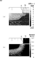
図2は、従来のCMOS型撮像素子における、フローティングディフュージョン領域の不純物分布と電界強度分布のシミュレーション結果を示したものである。図2(a)は、不純物濃度分布を示しており、図2(b)は、電界強度分布を示している。尚、図2(a)の不純物濃度分布においては、白色に近くなるほどn型不純物の濃度が高く、黒色に近くなるほどp型不純物の濃度が高いことを示している。また、図2(b)の電界強度分布においては、白色に近いほど電界強度が高く、黒色に近いほど電界強度が低いことを示している。また、図2(a),図2(b)においては、いずれも同図内に転送ゲートTGが存在し、フローティングディフュージョンFDが配置される場合を示している。換言すれば、図2は、いずれも、図1の転送ゲートTGおよびフローティングディフュージョンFD付近を拡大した範囲の分布が示されている。ここで、図2(b)においては、転送ゲートにはオフ時を想定し負電位が印加され、フローティングディフュージョンFD領域は正電位となっている。 FIG. 2 shows simulation results of impurity distribution and electric field strength distribution in the floating diffusion region in a conventional CMOS image sensor. FIG. 2A shows the impurity concentration distribution, and FIG. 2B shows the electric field strength distribution. In the impurity concentration distribution of FIG. 2A, the concentration of n-type impurities is higher as it is closer to white, and the concentration of p-type impurities is higher as it is closer to black. In addition, in the electric field intensity distribution of FIG. 2B, the closer to white, the higher the electric field intensity, and the closer to black, the lower the electric field intensity. 2A and 2B both show a case where the transfer gate TG is present in the same figure and the floating diffusion FD is disposed. In other words, FIG. 2 shows the distribution of the range in which the vicinity of the transfer gate TG and the floating diffusion FD in FIG. 1 is enlarged. Here, in FIG. 2B, a negative potential is applied to the transfer gate assuming that it is off, and the floating diffusion FD region is at a positive potential.
すなわち、図2で示す従来の構造の場合、転送ゲートTGがオフ時に、同転送ゲートTGに印加された負電位が、ゲート絶縁膜を介して、ゲート絶縁膜直下のシリコン基板Si内に伝えられる。その結果、同ゲート絶縁膜直下のシリコン基板とフローティングディフュージョンFD領域との電位差により、転送ゲートTG端付近(図2(b)中の領域A)に電界の最大値をとる領域が存在する。 That is, in the case of the conventional structure shown in FIG. 2, when the transfer gate TG is turned off, the negative potential applied to the transfer gate TG is transmitted through the gate insulating film into the silicon substrate Si immediately below the gate insulating film. . As a result, there is a region where the maximum value of the electric field exists near the end of the transfer gate TG (region A in FIG. 2B) due to the potential difference between the silicon substrate immediately below the gate insulating film and the floating diffusion FD region.
特に、CMOS型撮像素子のうち、グローバルシャッタ方式であって、特許文献2のような例でフローティングディフュージョンFDに信号電荷を保持する場合、リーク電流の影響が避けられない。すなわち、信号電荷の保持期間中に、前述した機構によって、フローティングディフュージョンFDにリーク電流が発生し続けることにより、転送されるべき信号電荷にノイズが生じ、SN比(Signal to Noise Ratio)が劣化する。
In particular, when a signal charge is held in the floating diffusion FD in the example of
従って、転送ゲートTG端のような結晶欠陥が生じ易い領域には、電界集中が生じない構造を実現し、リーク電流を低減できる構造とすることが望ましいと言える。 Therefore, it can be said that it is desirable to realize a structure in which electric field concentration does not occur in a region where a crystal defect is likely to occur, such as the end of the transfer gate TG, and to reduce the leakage current.
本発明はこのような状況に鑑みてなされたものであり、特に、CMOS型固体撮像素子のフローティングディフュージョンにおいて、転送ゲート端付近への電界集中を防止し、リーク電流の生じにくい固体撮像素子と、その製造方法を実現できるようにするものである。 The present invention has been made in view of such a situation, and in particular, in a floating diffusion of a CMOS type solid-state image sensor, a solid-state image sensor that prevents electric field concentration near the transfer gate end and is unlikely to generate a leakage current; The manufacturing method can be realized.
本発明の一側面の固体撮像素子は、光信号を信号電荷に変換するフォトダイオードと、前記フォトダイオードから信号電荷を転送する転送ゲートと、前記信号電荷が転送されるフローティングディフュージョンと、ゲートが前記フローティングディフュージョンに接続されるMOSトランジスタとを備え、前記フローティングディフュージョンを形成する第1導電型半導体層の転送ゲート端部に、第2導電型半導体層を形成する。 A solid-state imaging device according to one aspect of the present invention includes a photodiode that converts an optical signal into a signal charge, a transfer gate that transfers the signal charge from the photodiode, a floating diffusion that transfers the signal charge, and a gate that includes the gate And a MOS transistor connected to the floating diffusion, and a second conductivity type semiconductor layer is formed at a transfer gate end portion of the first conductivity type semiconductor layer forming the floating diffusion.
前記第1導電型半導体層および前記第2導電型半導体層は、相互に一部が接するように形成されるようにすることができる。 The first conductive semiconductor layer and the second conductive semiconductor layer may be formed so as to be partially in contact with each other.
前記第2導電型半導体からなる部位は、前記第1導電型半導体層の素子分離領域の周囲に形成された第2導電型半導体層と繋がるように形成することができる。 The portion made of the second conductivity type semiconductor may be formed so as to be connected to the second conductivity type semiconductor layer formed around the element isolation region of the first conductivity type semiconductor layer.
前記フローティングディフュージョンに接続された、リセット用トランジスタのソース領域におけるリセットゲート端部に、前記第2導電型半導体層を形成するようにさせることができる。 The second conductivity type semiconductor layer may be formed at the reset gate end portion in the source region of the reset transistor connected to the floating diffusion.
単位画素あたりに複数の前記フローティングディフュージョンと複数の前記転送ゲートを有する場合に、少なくとも1つ以上の前記フローティングディフュージョン形成する第1導電型半導体層の転送ゲート端部には、第2導電型半導体層を形成するようにさせることができる。 In the case where a plurality of floating diffusions and a plurality of transfer gates are provided per unit pixel, the second conductive semiconductor layer is formed at the transfer gate end of the first conductive semiconductor layer in which at least one floating diffusion is formed. Can be formed.
単位画素あたりに複数の前記フローティングディフュージョンと複数の前記転送ゲートを有する場合に、転送ゲートと転送ゲートに挟まれた、少なくとも1つ以上の前記フローティングディフュージョンにおいて、前記フローティングディフュージョンを形成する第1導電型半導体層の表面が、第2導電型半導体層で覆われているようにすることができる。 In the case where a plurality of floating diffusions and a plurality of transfer gates are provided per unit pixel, the first conductivity type that forms the floating diffusion in at least one of the floating diffusions sandwiched between the transfer gates and the transfer gates The surface of the semiconductor layer can be covered with the second conductivity type semiconductor layer.
本発明の固体撮像素子は、複数の画素全てが同時に撮像動作を行うグローバルシャッタ機能を有する固体撮像素子であって、前記フォトダイオードから前記フローティングディフュージョンへ全画素が同時に信号電荷の転送を行い、転送後から読み出しまでの間に前記フローティングディフュージョンで信号電荷を保持させるようにすることができる。 The solid-state imaging device of the present invention is a solid-state imaging device having a global shutter function in which all of a plurality of pixels perform imaging operation simultaneously, and all pixels simultaneously transfer signal charges from the photodiode to the floating diffusion. The signal charge can be held by the floating diffusion between later and read.
本発明の第2の側面の製造方法は、シリコン基板上にフォトダイオードを構成する第1導電型半導体層を形成する第1の工程と、転送ゲートを形成する第2の工程と、前記第1導電型半導体層を覆うと共に、フローティングディフュージョン領域の前記転送ゲート端部に、第2導電型半導体層を形成する第3の工程と、フローティングディフュージョンを構成する第1導電型半導体からなる層を形成する第4の工程とを含む。 The manufacturing method according to the second aspect of the present invention includes a first step of forming a first conductivity type semiconductor layer constituting a photodiode on a silicon substrate, a second step of forming a transfer gate, and the first step. A third step of forming a second conductive type semiconductor layer and a layer made of the first conductive type semiconductor constituting the floating diffusion are formed at the transfer gate end of the floating diffusion region while covering the conductive type semiconductor layer. And a fourth step.
本発明の電子機器は、光信号を信号電荷に変換するフォトダイオードと、前記フォトダイオードから信号電荷を転送する転送ゲートと、前記信号電荷が転送されるフローティングディフュージョンと、ゲートが前記フローティングディフュージョンに接続されるMOSトランジスタとを備え、前記フローティングディフュージョンを形成する第1導電型半導体層において、転送ゲート端部に、第2導電型半導体層が形成されてなることを特徴とした。 The electronic device of the present invention includes a photodiode that converts an optical signal into a signal charge, a transfer gate that transfers the signal charge from the photodiode, a floating diffusion that transfers the signal charge, and a gate connected to the floating diffusion. In the first conductive semiconductor layer forming the floating diffusion, a second conductive semiconductor layer is formed at the end of the transfer gate.
本発明の第1の側面においては、フォトダイオードにより光信号が信号電荷に変換され、転送ゲートにより、前記フォトダイオードから信号電荷がフローティングディフュージョンに転送され、フローティングディフュージョンにより、前記信号電荷が転送され、MOSトランジスタにより、ゲートが前記フローティングディフュージョンに接続され、前記フローティングディフュージョンを形成する第1導電型半導体層の転送ゲート端部に、第2導電型半導体層が形成される。 In the first aspect of the present invention, an optical signal is converted into a signal charge by a photodiode, a signal charge is transferred from the photodiode to a floating diffusion by a transfer gate, and the signal charge is transferred by a floating diffusion, A MOS transistor causes a gate to be connected to the floating diffusion, and a second conductivity type semiconductor layer is formed at a transfer gate end portion of the first conductivity type semiconductor layer forming the floating diffusion.
本発明の第2の側面においては、シリコン基板上にフォトダイオードを構成する第1導電型半導体層が形成され、さらに信号電荷をフローティングディフュージョンへ転送する転送ゲートが形成され、前記第1導電型半導体層が覆われると共に、フローティングディフュージョン領域の前記転送ゲート端部に、第2導電型半導体層が形成され、フローティングディフュージョンを構成する第1導電型半導体層が形成される。 In the second aspect of the present invention, a first conductive semiconductor layer constituting a photodiode is formed on a silicon substrate, and a transfer gate for transferring signal charges to a floating diffusion is formed. A layer is covered, and a second conductivity type semiconductor layer is formed at the transfer gate end portion of the floating diffusion region, and a first conductivity type semiconductor layer constituting the floating diffusion is formed.
本発明によれば、フローティングディフュージョンにおいて、結晶欠陥が生じ易い転送ゲートTG端付近への電界集中を防ぎ、リーク電流を抑制することが可能となる。また、フローティングディフュージョンを形成する不純物層が転送ゲートTGに対しオーバーラップしない構造となるため、転送ゲート端部におけるオーバーラップ容量が低減し、変換効率が増大する。この結果、高いSN比での撮像が可能となる。 According to the present invention, in floating diffusion, it is possible to prevent electric field concentration near the end of the transfer gate TG where crystal defects are likely to occur, and to suppress leakage current. Further, since the impurity layer forming the floating diffusion does not overlap with the transfer gate TG, the overlap capacitance at the end of the transfer gate is reduced and the conversion efficiency is increased. As a result, imaging with a high S / N ratio is possible.
以下、発明を実施するための最良の形態(以下実施の形態とする)について説明する。尚、説明は以下の順序で行う
1.第1の実施の形態(基本例)
2.第2の実施の形態(素子分離領域の周囲が第2導電型半導体層に囲まれた例)
3.第3の実施の形態(リセットトランジスタのソース領域にフローティングディフュージョンが接続された例)
4.第4の実施の形態(転送ゲートとフローティングディフュージョンを複数有する例)
Hereinafter, the best mode for carrying out the invention (hereinafter referred to as an embodiment) will be described. The description will be given in the following order. First embodiment (basic example)
2. Second Embodiment (Example in which the periphery of an element isolation region is surrounded by a second conductivity type semiconductor layer)
3. Third Embodiment (Example in which floating diffusion is connected to source region of reset transistor)
4). Fourth embodiment (example having a plurality of transfer gates and floating diffusions)
<第1の実施の形態>
[固体撮像素子を含む1画素分の回路構成]
本発明を適用した固体撮像素子の構成についての説明にあたり、まず、固体撮像素子を含む1画素分の回路構成について説明する。
<First Embodiment>
[Circuit configuration for one pixel including a solid-state image sensor]
In describing the configuration of the solid-state imaging device to which the present invention is applied, first, a circuit configuration for one pixel including the solid-state imaging device will be described.
図3は、固体撮像素子を含む1画素分の回路構成を示している。図3に示すように、固体撮像素子を含む1画素分の回路構成は、フォトダイオード21、フローティングディフュージョン部(FD)22、および複数のMOSトランジスタTr1乃至Tr4を含む構成とされている。図3における複数のMOSトランジスタTr1乃至Tr4は、それぞれ転送トランジスタTr1、リセットトランジスタTr2、増幅トランジスタTr3、および選択トランジスタTr4である。
FIG. 3 shows a circuit configuration for one pixel including the solid-state imaging device. As shown in FIG. 3, the circuit configuration for one pixel including the solid-state imaging device includes a
転送トランジスタTr1は、フォトダイオード21からなるソース、フローティングディフュージョン部22からなるドレイン、および、そのソース・ドレイン間に形成されたゲート電極24から構成されている。転送トランジスタTr1においては、ゲート電極24に転送パルスφTRGが供給される。これにより、受光部21に蓄積された信号電荷がフローティングディフュージョン部22に転送される。尚、受光部21は、後述するフォトダイオードPDである。
The transfer transistor Tr1 includes a source composed of a
増幅トランジスタTr3は、電源VDDからなるソース、不純物領域23からなるドレイン、およびそのソース・ドレイン間に形成されたゲート電極26から構成されている。
The amplifying transistor Tr3 includes a source composed of a power supply VDD, a drain composed of an
ここで、フローティングディフュージョン部22と増幅トランジスタTr3のゲート電極26は、電気的に接続される必要がある。すなわち、フローティングディフュージョン部22と増幅トランジスタTr3のゲート電極26とが電気的に接続されることにより、増幅トランジスタTr3では、ゲート電極26にフローティングディフュージョン部22の電位が供給される。これにより、フローティングディフュージョン部22の電位に対応した画素信号が、増幅トランジスタTr3のドレインとなる不純物領域23に出力される。
Here, the floating
リセットトランジスタTr2は、フローティングディフュージョン部22からなるソースと、電源VDDからなるドレインと、そのソース・ドレイン間に形成されたゲート電極25とから構成されている。リセットトランジスタTr2においては、ゲート電極25にリセットパルスφRSTが供給される。これにより、フローティングディフュージョン部22の電位が、電源VDDの電源電位付近の電位にリセットされる。
The reset transistor Tr2 includes a source including the floating
選択トランジスタTr4は、不純物領域23からなるソース、垂直信号線VSLに接続された不純物領域28からなるドレインと、そのソース・ドレイン間に形成されたゲート電極27とから構成されている。ここで、選択トランジスタTr4のソースとなる不純物領域23は、増幅トランジスタTr3のドレインと共用される。選択トランジスタTr4においては、ゲート電極27に選択パルスφSELが供給される。これにより不純物領域23に流れ込んだ画素信号が垂直信号線VSLより伝送される。
The selection transistor Tr4 includes a source composed of the
尚、図3においては、フローティングディフュージョン部が1箇所設けられる例を示しているが、フローティングディフュージョン部は、複数箇所に設けられる構成としてもよい。 Although FIG. 3 shows an example in which one floating diffusion portion is provided, the floating diffusion portion may be provided at a plurality of locations.
[固体撮像素子の構成例]
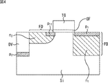
図4は、本発明を適用した一実施の形態の構成例を示す固体撮像素子である。
[Configuration example of solid-state image sensor]
FIG. 4 is a solid-state imaging device showing a configuration example of an embodiment to which the present invention is applied.
固体撮像素子は、シリコン基板Si上に第1導電型半導体層としてn型不純物層n1が設けられ、その上部に第2導電型半導体層としてp型不純物層p1が設けられている。そして、この層p1,n1によりフォトダイオードPDが形成されている。また、図中には素子分離領域DVが設けられており、その下には、p型不純物層p2が設けられている。さらに、転送ゲートTGは、ゲート絶縁膜GF上に設けられている。そして、フォトダイオードPDに対し転送ゲートTGを挟んだ位置に、第1導電型半導体層であるn型不純物層n2により形成された、フローティングディフュージョンFDが設けられている。フローティングディフュージョンFDを形成するn型不純物層n2の転送ゲートTG端部には、第2導電型半導体層としてp型不純物層p11が形成されている。より詳細には、転送ゲートTG端部に対し、p型不純物層p11は一部の面がオーバーラップするように形成される。 In the solid-state imaging device, an n-type impurity layer n1 is provided as a first conductive type semiconductor layer on a silicon substrate Si, and a p-type impurity layer p1 is provided as a second conductive type semiconductor layer thereon. A photodiode PD is formed by the layers p1 and n1. In the drawing, an element isolation region DV is provided, and a p-type impurity layer p2 is provided below the element isolation region DV. Further, the transfer gate TG is provided on the gate insulating film GF. A floating diffusion FD formed by an n-type impurity layer n2 which is a first conductivity type semiconductor layer is provided at a position sandwiching the transfer gate TG with respect to the photodiode PD. A p-type impurity layer p11 is formed as a second conductivity type semiconductor layer at the end of the transfer gate TG of the n-type impurity layer n2 forming the floating diffusion FD. More specifically, the p-type impurity layer p11 is formed so that a part of the surface overlaps the end portion of the transfer gate TG.
[図4の固体撮像素子における不純物濃度分布と電界強度分布]
このp型不純物層p11が形成されることにより、図5(b)で示されるように、フローティングディフュージョンFDの転送ゲートTG端部に発生していた電界集中を抑制することが可能となっている。図5(a)は、図4の本発明の固体撮像素子における不純物濃度分布を示し、図5(b)は、その電界強度分布を示している。ここで、図5(b)においては、転送ゲートはオフ時を想定し負電位が印加され、フローティングディフュージョンFD領域は正電位となっているまた、図5(a)の不純物濃度分布においては、白色に近くなるほどn型不純物の濃度が高く、黒色に近くなるほどp型不純物の濃度が高いことを示している。また、図5(b)の電界強度分布においては、白色に近いほど電界強度が高く、黒色に近いほど電界強度が低いことを示している。さらに、図5(a),図5(b)においては、いずれも同図内に転送ゲートTGが存在し、フローティングディフュージョンFDが配置される場合を示している。換言すれば、図5は、いずれも、図4の転送ゲートTGおよびフローティングディフュージョンFD付近を拡大した範囲の分布が示されている。
[Impurity distribution and electric field strength distribution in the solid-state imaging device of FIG. 4]
By forming the p-type impurity layer p11, as shown in FIG. 5B, it is possible to suppress the electric field concentration generated at the end of the transfer gate TG of the floating diffusion FD. . FIG. 5A shows the impurity concentration distribution in the solid-state imaging device of the present invention shown in FIG. 4, and FIG. 5B shows the electric field strength distribution. Here, in FIG. 5B, a negative potential is applied to the transfer gate assuming that it is off, and the floating diffusion FD region is a positive potential. In the impurity concentration distribution of FIG. The closer to white, the higher the concentration of n-type impurities, and the closer to black, the higher the concentration of p-type impurities. Further, in the electric field intensity distribution of FIG. 5 (b), the closer to white, the higher the electric field intensity, and the closer to black, the lower the electric field intensity. 5 (a) and 5 (b) both show a case where the transfer gate TG exists in the same figure and the floating diffusion FD is arranged. In other words, FIG. 5 shows the distribution of the range in which the vicinity of the transfer gate TG and the floating diffusion FD in FIG. 4 is enlarged.
ここで、図4で示される本発明の固体撮像素子の構造と、図1で示される従来の固体撮像素子の構造との違いは、p型不純物層p11の有無である。 Here, the difference between the structure of the solid-state imaging device of the present invention shown in FIG. 4 and the structure of the conventional solid-state imaging device shown in FIG. 1 is the presence or absence of the p-type impurity layer p11.
すなわち、図1の従来構造の固体撮像素子における、図2のシミュレーション結果については以下のように説明できる。すなわち、転送ゲートTGがオフ時に印加される負電位が、ゲート絶縁膜GFを介してシリコン基板Si内のチャネル部に伝えられ、同チャネル部とフローティングディフュージョンFDとが電位差を生じる。この結果、転送ゲートTG端付近に電界の最大値を示す箇所が生じていた。 That is, the simulation result of FIG. 2 in the solid-state imaging device having the conventional structure of FIG. 1 can be described as follows. That is, a negative potential applied when the transfer gate TG is turned off is transmitted to the channel portion in the silicon substrate Si through the gate insulating film GF, and a potential difference is generated between the channel portion and the floating diffusion FD. As a result, a portion showing the maximum value of the electric field is generated near the end of the transfer gate TG.
そこで、図4で示されるように、n型不純物層n2の転送ゲートTG端付近にp型不純物層p11(図5(a)の領域Bの黒色部分)を設けるようにした。この結果、pn接合部が転送ゲートTGからフローティングディフュージョンFDに向かって離れる方向に、図5(b)の領域A’に移動する。すなわち、図5(b)で示されるように、転送ゲートTG端での電界集中が抑制される。 Therefore, as shown in FIG. 4, the p-type impurity layer p11 (the black portion of the region B in FIG. 5A) is provided near the end of the transfer gate TG of the n-type impurity layer n2. As a result, the pn junction moves to the region A ′ in FIG. 5B in a direction away from the transfer gate TG toward the floating diffusion FD. That is, as shown in FIG. 5B, electric field concentration at the transfer gate TG end is suppressed.
すなわち、図4に示す本発明の構成をとることで、結晶欠陥の生じ易い転送ゲートTG端への電界集中が抑制され、結晶欠陥を介したリーク電流の発生を抑制することが可能となる。また、本発明の構成では、フローティングディフュージョンを形成するn型不純物層n2が転送ゲートTGに対しオーバーラップしなくなる。この結果、転送ゲートTGとn型不純物層n2間で生じるオーバーラップ容量が、図1の従来構造の場合に比べ低減する。このように、フローティングディフュージョンの寄生容量が低減するため、変換効率が増大する。以上、本発明を成すことで、暗時や低照度での撮像において発生しやすいノイズを低減することが可能となる。 That is, by adopting the configuration of the present invention shown in FIG. 4, electric field concentration at the transfer gate TG end where crystal defects are likely to occur can be suppressed, and generation of leakage current via the crystal defects can be suppressed. In the configuration of the present invention, the n-type impurity layer n2 forming the floating diffusion does not overlap the transfer gate TG. As a result, the overlap capacitance generated between the transfer gate TG and the n-type impurity layer n2 is reduced as compared with the conventional structure of FIG. Thus, since the parasitic capacitance of the floating diffusion is reduced, the conversion efficiency is increased. As described above, according to the present invention, it is possible to reduce noise that is likely to occur in imaging in the dark or at low illuminance.
また、特に、グローバルシャッタ方式のCMOS型撮像素子においては、信号電荷の保持期間におけるノイズを低減させることが可能となる。 In particular, in the global shutter CMOS image sensor, noise during the signal charge holding period can be reduced.
[ローリングシャッタ方式]
例えば、ローリングシャッタ方式(フォーカルプレーンシャッタ方式、またはライン露光方式とも称する)においては、図6で示されるように、行単位でフォトダイオードの露光が開始され、露光終了と同時に読み出しが開始される。すなわち、図6においては、第1行目においては、時刻t1で露光が開始され、露光期間Teが経過した時刻t101に露光が終了すると読出期間Trが開始される。第2行目においては、時刻t2で露光が開始され、露光期間Teが経過した時刻t102に露光が終了すると読出期間Trが開始される。時刻t3で露光が開始され、露光期間Teが経過した時刻t103に露光が終了すると読出期間Trが開始される。そして、第1行目においては、時刻t103で再び露光が開始され、露光期間Teが経過したとき、露光が終了し、同時に読出期間Trが開始され、この処理が順次繰り返される。このため、ローリングシャッタ方式においては、撮像された画像は、行単位で露光期間がずれるため、行単位で異なるタイミングの画像が撮像されることになり、行単位の画像を組み合わせて1枚の画像を構成すると歪が生じやすい。しかしながら、ローリングシャッタ方式では、信号電荷の保持時間がないため、リーク電流に起因するノイズが比較的生じ難い。
[Rolling shutter system]
For example, in the rolling shutter method (also referred to as a focal plane shutter method or a line exposure method), as shown in FIG. 6, exposure of photodiodes is started in units of rows, and reading is started simultaneously with the end of exposure. That is, in FIG. 6, in the first row, the exposure starts at time t1, and when the exposure ends at time t101 when the exposure period Te has elapsed, the readout period Tr starts. In the second row, the exposure starts at time t2, and when the exposure ends at time t102 when the exposure period Te has elapsed, the readout period Tr starts. The exposure is started at time t3, and when the exposure ends at time t103 when the exposure period Te has elapsed, the readout period Tr is started. In the first row, the exposure is started again at time t103, and when the exposure period Te has elapsed, the exposure is completed, and at the same time, the reading period Tr is started, and this process is sequentially repeated. For this reason, in the rolling shutter system, since the exposure period of the captured image is shifted in units of rows, images at different timings are captured in units of rows, and one image is obtained by combining the images in units of rows. If it is configured, distortion is likely to occur. However, in the rolling shutter system, since there is no signal charge holding time, noise due to leakage current is relatively difficult to occur.
[グローバルシャッタ方式]
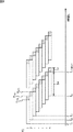
一方、グローバルシャッタ方式においては、図7で示されるように、全行が同時に露光を開始し、露光期間Teが終了すると、行単位で順次読み出しがなされていく。すなわち、図7においては、時刻t201において、全行のフォトダイオードの露光が一斉に開始され、露光期間Teが終了する時刻t301に一斉に露光が終了すると、行単位で読出期間Trで順次信号電荷が読み出されていく。この結果、先頭行に近い行は保持期間Tk1に近く短い期間で済むが、最終行に近い行は、保持期間Tknに近く期間が長くなる。尚、Tknの「n」は行番号である。
[Global shutter system]
On the other hand, in the global shutter system, as shown in FIG. 7, all rows start exposure at the same time, and when the exposure period Te ends, reading is sequentially performed in units of rows. That is, in FIG. 7, exposure of the photodiodes of all rows starts at the same time at time t201, and when the exposure ends at the same time at time t301 when the exposure period Te ends, the signal charges are sequentially transferred in the readout period Tr in units of rows. Is read out. As a result, a row close to the first row needs a short period close to the holding period Tk1, but a row close to the final line has a period close to the holding period Tkn. Note that “n” in Tkn is a row number.
従って、図1の従来の固体撮像素子では、転送ゲートTG端部に電界集中が発生することによりリーク電流が発生する状態で、この保持期間Tknが継続すると、保持期間Tknに比例して信号電荷にノイズが蓄積されることになり、画質を劣化させる可能性がある。 Therefore, in the conventional solid-state imaging device of FIG. 1, when this holding period Tkn continues in a state where leakage current is generated due to electric field concentration at the end of the transfer gate TG, the signal charge is proportional to the holding period Tkn. Noise is accumulated in the image, which may degrade the image quality.
これに対して、図4の本発明の固体撮像素子では、n型不純物層n2の転送ゲートTG端付近にp型不純物層p11が設けられることで、転送ゲートTG端での電界集中を防止することができる。結果として、図4の本発明の固体撮像素子は、グローバルシャッタ方式などの保持期間Tknが長い画素を含むようなシャッタ方式では、リーク電流の発生を抑制できる分、ノイズを低減させる効果が大きい。 On the other hand, in the solid-state imaging device of the present invention of FIG. 4, the p-type impurity layer p11 is provided in the vicinity of the transfer gate TG end of the n-type impurity layer n2, thereby preventing electric field concentration at the transfer gate TG end. be able to. As a result, the solid-state imaging device of the present invention shown in FIG. 4 has a great effect of reducing noise by the amount of leakage current that can be suppressed in a shutter method including a pixel having a long holding period Tkn such as the global shutter method.
[図4の固体撮像素子の製造方法について]
次に、図8のフローチャートを参照して、図4で示される固体撮像素子の製造処理について説明する。
[Method for Manufacturing Solid-State Imaging Device in FIG. 4]
Next, a manufacturing process of the solid-state imaging device shown in FIG. 4 will be described with reference to the flowchart of FIG.
ステップS1において、図9(a)で示されるように、シリコン基板Si上に素子分離領域DVが形成される。ここで、素子分離領域DVの形成方法は、例えば、シリコン基板Siの選択酸化によるLOCOS(Local Oxidation of Silicon)法、もしくは、浅い溝に絶縁膜を埋め込むSTI(Shallow Trench Isolation)法、または、素子分離領域DVにp型不純物層を形成する不純物分離法のどの方法によるものでもかまわない。ここで、素子分離領域DVがLOCOS法またはSTI法により形成される場合は、その形成前、または形成後に、チャネルストッパ用のp型不純物層p2が素子分離領域DV下に形成される。 In step S1, as shown in FIG. 9A, an element isolation region DV is formed on the silicon substrate Si. Here, a method for forming the element isolation region DV is, for example, a LOCOS (Local Oxidation of Silicon) method by selective oxidation of a silicon substrate Si, an STI (Shallow Trench Isolation) method in which an insulating film is embedded in a shallow trench, or an element Any impurity separation method for forming a p-type impurity layer in the isolation region DV may be used. Here, when the element isolation region DV is formed by the LOCOS method or the STI method, the p-type impurity layer p2 for channel stopper is formed under the element isolation region DV before or after the formation.
ステップS2において、図9(b)で示されるように、イオン注入が行われ、フォトダイオードPDを構成する第1導電型半導体層であるn型不純物層n1が形成される。 In step S2, as shown in FIG. 9B, ion implantation is performed to form an n-type impurity layer n1, which is a first conductivity type semiconductor layer constituting the photodiode PD.
ステップS3において、図9(c)で示されるように、ゲート絶縁膜GFが形成され、その上にポリシリコン(Poly-Si)などからなる転送ゲートTGが形成される。 In step S3, as shown in FIG. 9C, a gate insulating film GF is formed, and a transfer gate TG made of polysilicon (Poly-Si) or the like is formed thereon.
ステップS4において、図9(d)で示されるように、フォトレジストPRをマスクとして用いフォトダイオードPDが形成される第1導電型半導体層の層n1の表面にB(ボロン)またはBF2(フッ化ボロン)のイオン注入が行われる。そして、同時に、フローティングディフュージョンFDが形成される領域にも、BまたはBF2のイオン注入が行われる。この結果、フォトダイオードPDの表面に第2導電型半導体層であるp型不純物層の層p1が形成されると同時に、フローティングディフュージョンFDの転送ゲートTG端付近に第2導電型半導体層である層p11が、転送ゲートTGに対して自己整合的に形成される。 In step S4, as shown in FIG. 9D, B (boron) or BF2 (fluorinated) is formed on the surface of the layer n1 of the first conductivity type semiconductor layer where the photodiode PD is formed using the photoresist PR as a mask. Boron) ion implantation is performed. At the same time, ion implantation of B or BF2 is also performed in the region where the floating diffusion FD is formed. As a result, a layer p1 of a p-type impurity layer which is a second conductivity type semiconductor layer is formed on the surface of the photodiode PD, and at the same time, a layer which is a second conductivity type semiconductor layer near the transfer gate TG end of the floating diffusion FD. p11 is formed in a self-aligned manner with respect to the transfer gate TG.
この処理において、注入時のイオン種としてB(ボロン)を用いる場合、その注入エネルギーは、例えば20keV以内とし、BF2を用いる場合、例えば50keV以内とする。また、いずれの場合にも、その注入量は、1e12/cm2以上とする。
In this process, when B (boron) is used as an ion species at the time of implantation, the implantation energy is, for example, within 20 keV, and when
ステップS5において、図9(e)で示されるように、フローティングディフュージョンFDに、1e13/cm2以上の燐または砒素のイオン注入が行われ、第1導電型半導体層であるn型不純物層n2が形成される。
In step S5, as shown in FIG. 9E, phosphorus or arsenic ions of 1e13 /
ステップS6において、RTA(Rapid Thermal Annealing)などの熱処理により、注入した不純物の活性化が行われる。 In step S6, the implanted impurities are activated by heat treatment such as RTA (Rapid Thermal Annealing).
尚、以上の製造処理において、フローティングディフュージョンFDの第1導電型半導体層を形成する方法は、転送ゲートTG側壁にサイドウォールスペーサを形成したのち、砒素または燐の不純物注入により拡散層が形成される方法でもよい。 In the above manufacturing process, in the method of forming the first conductive type semiconductor layer of the floating diffusion FD, after forming the sidewall spacer on the side wall of the transfer gate TG, the diffusion layer is formed by impurity implantation of arsenic or phosphorus. The method may be used.
また、転送ゲートTG形成後に1e13/cm2乃至1e14/cm2程度の燐または砒素の不純物注入が行われた後、転送ゲートTG側壁にサイドウォールスペーサが形成されるようにする。さらに、砒素または燐の不純物注入により不純物拡散層が形成され、LDD(Lightly Doped Drain)構造の形態としてもよい。 In addition, after the transfer gate TG is formed, phosphorous or arsenic impurities of about 1e13 / cm2 to 1e14 / cm2 are implanted, and then sidewall spacers are formed on the side walls of the transfer gate TG. Further, an impurity diffusion layer may be formed by impurity implantation of arsenic or phosphorous, and an LDD (Lightly Doped Drain) structure may be employed.
以上の製造処理によれば、フローティングディフュージョンFDの転送ゲートTG端付近に第2導電型半導体層であるp型不純物層p11は、フォトダイオードPD表面の第2導電型半導体層であるp型不純物層p1と同時に形成される。このため、従来の製造工程において、フォトダイオードPD表面の第2導電型半導体層であるp型不純物層p1が形成される処理における、処理範囲を層p11が形成されるために一部拡大するのみで、図4の固体撮像素子を製造することが可能となる。結果として、従来の製造工程に対し、新たな工程を加えることなく、低コストで、かつ、容易にリーク電流を低減する固体撮像素子を製造することが可能となる。 According to the above manufacturing process, the p-type impurity layer p11 which is the second conductivity type semiconductor layer near the transfer gate TG end of the floating diffusion FD is the p-type impurity layer which is the second conductivity type semiconductor layer on the surface of the photodiode PD. It is formed simultaneously with p1. For this reason, in the conventional manufacturing process, in the process of forming the p-type impurity layer p1 which is the second conductivity type semiconductor layer on the surface of the photodiode PD, the processing range is only partially enlarged because the layer p11 is formed. Thus, it becomes possible to manufacture the solid-state imaging device of FIG. As a result, it is possible to manufacture a solid-state imaging device that easily reduces the leakage current at low cost without adding a new process to the conventional manufacturing process.
<第2の実施の形態>
[素子分離領域の周囲が第2導電型半導体層に囲まれた構成例]
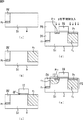
以上においては、フローティングディフュージョンFDの転送ゲート端部に第2導電型半導体層として層p11が形成される例について説明してきたが、この位置関係が維持されていれば、層p11は、他の範囲に存在する構成としてもよい。例えば、図10で示されるように、層p11に代えて構成される層p21を設けるようにしてもよい。この層p21は、フローティングディフュージョンFDを表面で囲み、さらに、素子分離領域DVを積層状に囲い込む構成となっている。尚、図10(a)は、平面図であり、図10(b)は、図10(a)のA-A’の断面図である。
<Second Embodiment>
[Configuration example in which the periphery of the element isolation region is surrounded by the second conductivity type semiconductor layer]
In the above, the example in which the layer p11 is formed as the second conductivity type semiconductor layer at the transfer gate end portion of the floating diffusion FD has been described. However, if this positional relationship is maintained, the layer p11 has a different range. It is good also as a structure which exists in. For example, as shown in FIG. 10, a layer p21 configured in place of the layer p11 may be provided. This layer p21 has a configuration in which the floating diffusion FD is surrounded by the surface, and the element isolation region DV is surrounded in a stacked manner. 10A is a plan view, and FIG. 10B is a cross-sectional view taken along line AA ′ of FIG. 10A.
このような層p21は、素子分離領域DVの形成前または形成後に、不純物注入により素子分離領域DVの周囲を積層状に覆うようにp型不純物層として形成されるようにすることで実現される。 Such a layer p21 is realized by forming a p-type impurity layer so as to cover the periphery of the element isolation region DV in a stacked manner by impurity implantation before or after the element isolation region DV is formed. .
このような構成とすることで、結晶欠陥の生じ易い転送ゲートTG端への電界集中を防止し、フローティングディフュージョンFDおけるリーク電流を低減できることは当然のことながら、さらに、素子分離領域DVの近傍で生じるリーク電流をも低減することが可能となる。結果として、転送ゲートTGと素子分離領域DVとのいずれのリーク電流も低減させることができるので、さらに、暗時、または低照度時における撮像画像におけるノイズを低減させることが可能となる。 By adopting such a configuration, it is possible to prevent electric field concentration at the end of the transfer gate TG where a crystal defect is likely to occur, and to reduce the leakage current in the floating diffusion FD. In addition, in the vicinity of the element isolation region DV. It is possible to reduce the generated leakage current. As a result, since any leakage current between the transfer gate TG and the element isolation region DV can be reduced, it is possible to further reduce noise in the captured image in the dark or at low illuminance.
<第3の実施の形態>
[リセットトランジスタのソース領域にフローティングディフュージョンが接続された構成例]
以上は、フローティングディフュージョンFDにおいて、結晶欠陥の生じ易い転送ゲートTG端部付近に層p11または層p21を形成する例について説明してきたが、結晶欠陥の生じ易い位置であれば、転送ゲートTG端部でなくとも同様の効果が得られる。
<Third Embodiment>
[Configuration example in which floating diffusion is connected to source region of reset transistor]
The above has described the example in which the layer p11 or the layer p21 is formed in the vicinity of the end of the transfer gate TG where the crystal defect is likely to occur in the floating diffusion FD. Even if not, the same effect can be obtained.
例えば、図11で示されるように、転送ゲートTGに加えて、リセットゲートRGを含むリセットトランジスタRSTを形成し、フローティングディフュージョンFDに接続されたリセットトランジスタRSTのソース領域Ssに、層p11と同様に第2導電型半導体層であるp型不純物層p53を設けるようにしてもよい。 For example, as shown in FIG. 11, in addition to the transfer gate TG, a reset transistor RST including a reset gate RG is formed, and in the source region Ss of the reset transistor RST connected to the floating diffusion FD, similarly to the layer p11. A p-type impurity layer p53 which is a second conductivity type semiconductor layer may be provided.
ここで、フローティングディフュージョンを形成するn型不純物層n2と,リセットトランジスタRSTのソース領域Ssを形成するn型不純物層n51は、配線Lにより同電位とされている。ただし、層n2,n51が一体となって形成されていれば、配線Lは不要となる。 Here, the n-type impurity layer n2 forming the floating diffusion and the n-type impurity layer n51 forming the source region Ss of the reset transistor RST are set to the same potential by the wiring L. However, if the layers n2 and n51 are integrally formed, the wiring L is not necessary.
このような構成により、フローティングディフュージョンFDの転送ゲートTG端部において生じる電界集中を防止することができ、フローティングディフュージョンおけるリーク電流を低減することができるだけでなく、フローティングディフュージョンFDに接続されたリセットトランジスタRSTのソース領域においても、同様のリーク電流をも低減することができる。<第4の実施の形態>
[転送ゲートとフローティングディフュージョンが複数に接続された構成例]
以上においては、転送ゲートとフローティングディフュージョンがそれぞれ1個の場合、または、リセットゲートとソース領域がそれぞれ1個の場合の例について説明してきたが、複数の構成であってもよいものである。
With such a configuration, it is possible to prevent electric field concentration occurring at the end of the transfer gate TG of the floating diffusion FD, not only to reduce the leakage current in the floating diffusion, but also to the reset transistor RST connected to the floating diffusion FD. Even in the source region, a similar leakage current can be reduced. <Fourth embodiment>
[Configuration example with multiple transfer gates and floating diffusions connected]
In the above description, an example in which there is one transfer gate and one floating diffusion, or one reset gate and one source region has been described, but a plurality of configurations may be used.
例えば、図12(a)で示されるように、2つのフローティングディフュージョンFD1,FD2と転送ゲートTG1,TG2を有する構造で、当該フローティングディフュージョンFD1,FD2の各転送ゲートTG1,TG2の端部に、それぞれ第2導電型半導体層であるp型不純物層p11,p71,p72が設けられている。すなわち、p型不純物層p11,p71,p72は、フローティングディフュージョンFD1,FD2を構成する第1導電型半導体層である層n71,n72の、転送ゲートTG1,TG2の端部に設けられている。このため、いずれにおいても、結晶欠陥が生じ易い転送ゲート端部での電界集中を防止することができるので、電界集中に起因するリーク電流を低減させることが可能となる。 For example, as shown in FIG. 12A, a structure having two floating diffusions FD1 and FD2 and transfer gates TG1 and TG2, and at the ends of the transfer gates TG1 and TG2 of the floating diffusions FD1 and FD2, respectively. P-type impurity layers p11, p71, and p72 which are second conductivity type semiconductor layers are provided. That is, the p-type impurity layers p11, p71, and p72 are provided at the ends of the transfer gates TG1 and TG2 of the layers n71 and n72, which are the first conductivity type semiconductor layers constituting the floating diffusions FD1 and FD2. Therefore, in any case, since electric field concentration at the transfer gate end portion where crystal defects are likely to occur can be prevented, leakage current resulting from electric field concentration can be reduced.
また、層p11,p71は、一体となって表層で層n71を取り囲むように構成してもよい。具体的には、図12(b)で示されるように、層p11,p71が一体となって、層p101を構成し、層n71の表面を覆い隠すようにしても同様の効果を得ることが可能である。 Further, the layers p11 and p71 may be integrated so as to surround the layer n71 as a surface layer. Specifically, as shown in FIG. 12B, the same effect can be obtained even when the layers p11 and p71 are integrated to form the layer p101 and cover the surface of the layer n71. Is possible.
尚、以上においては、第1導電型半導体層および第2導電型半導体層は、それぞれn型不純物層およびp型不純物層である場合について説明してきていたが、当然のことながら、それぞれp型不純物層およびn型不純物層として入替えても同様の効果を奏するものである。 In the above description, the case where the first conductive type semiconductor layer and the second conductive type semiconductor layer are an n-type impurity layer and a p-type impurity layer, respectively, has been described. Even if the layers and the n-type impurity layer are replaced, the same effect can be obtained.
[本発明の固体撮像素子を適用した電子機器の構成例]
次に、図13を参照して、本発明の固体撮像素子を適用した電子機器の構成例について説明する。尚、図13において、図13(a)は、本発明を適用した固体撮像素子からなる固体撮像装置101の概略構成図であり、図13(b)は、電子機器131の概略断面図である。
[Configuration example of electronic apparatus to which the solid-state imaging device of the present invention is applied]
Next, a configuration example of an electronic apparatus to which the solid-state imaging device of the present invention is applied will be described with reference to FIG. In FIG. 13, FIG. 13A is a schematic configuration diagram of a solid-
固体撮像装置1は、図13(a)で示されるように、各単位画素がアレイ状に配置された画素アレイ部111、制御回路112、垂直駆動回路113、カラム信号処理回路114、水平駆動回路115、および出力回路116を備えている。制御回路112は、垂直駆動回路113、カラム信号処理回路114、および水平駆動回路115を制御している。垂直駆動回路113、カラム信号処理回路114、および水平駆動回路115は、垂直信号線L1および画素駆動線L2を用いて、画素アレイ部111の画素信号を転送し、出力回路116より出力させる。
As shown in FIG. 13A, the solid-
図13(b)の電子機器131は、上述した本発明の画素を含む固体撮像装置101を用いた場合の構成例であり、例えば、静止画撮影が可能なデジタルカメラなどである。
An
電子機器131は、固体撮像装置101、光学レンズ141、シャッタ装置142と、駆動回路143、および信号処理回路144を備えている。
The
光学レンズ141は、被写体からの像光(入射光)を固体撮像装置101の撮像面上に結像させる。これにより固体撮像装置101内に一定期間当該信号電荷が蓄積される。シャッタ装置142は、固体撮像装置101への光照射期間および遮光期間を制御する。駆動回路143は、固体撮像装置101の転送動作およびシャッタ装置142のシャッタ動作を制御する駆動信号を供給する。駆動回路143は、固体撮像装置101に対して駆動信号(タイミング信号)を供給し、固体撮像装置101は、この駆動信号に基づいて信号転送を行い、画像信号として信号処理回路144に供給する。信号処理回路144は、個体撮像装置101より供給されてくる画像信号に対して各種の信号処理を行う。信号処理が行われた映像信号は、図示せぬメモリなどの記憶媒体に記憶されたり、または、LCD(Liquid Cryustal Display)などからなるモニタに出力されて表示される。
The
図13(b)の電子機器131では、本発明の固体撮像素子を適用した固体撮像装置101を用いることにより、固体撮像装置101のフローティングディフュージョンにおいては、結晶欠陥が生じ易い転送ゲート端付近への電界集中を防止し、リーク電流を抑制することが可能となる。また、転送ゲート端部におけるオーバーラップ容量が低減し、変換効率が増大する。このため電子機器131では、高いSN比での撮像が可能となる。
In the
尚、本発明の固体撮像素子を用いた固体撮像装置101を適用できる電子機器131としては、デジタルカメラに限られるものではなく、デジタルスチルカメラ、さらには携帯電話機等のモバイル機器向けカメラモジュールなどの撮像装置に適用可能である。
Note that the
本発明によれば、フローティングディフュージョンFDにおいて、結晶欠陥が生じ易い転送ゲート端付近への電界集中を防止することができるので、リーク電流が抑制され、低照度時、または暗時に、ノイズを低減して画像を撮像することが可能となる。特に、グローバルシャッタ方式のシャッタによる固体撮像素子の場合、読み出し動作までの間、フローティングディフュージョンFDに長時間、信号電荷が保持されることとなるので、リーク電流を低減させることにより、ノイズの少ない撮像が可能となる。 According to the present invention, in the floating diffusion FD, electric field concentration near the transfer gate end where crystal defects are likely to occur can be prevented, so that leakage current is suppressed and noise is reduced at low illuminance or darkness. Thus, an image can be taken. In particular, in the case of a solid-state imaging device using a global shutter type shutter, signal charges are held in the floating diffusion FD for a long time until the reading operation. Therefore, imaging with less noise can be performed by reducing the leakage current. Is possible.
尚、本明細書において、処理工程を記述するステップは、記載された順序に沿って時系列的に行われる処理は、もちろん、必ずしも時系列的に処理されなくとも、並列的あるいは個別に実行されても構わない。 In the present specification, the steps describing the processing steps are executed in parallel or individually even if not necessarily time-sequentially processed, of course, in a time-series manner according to the described order. It doesn't matter.
TG,TG1,TG2 転送ゲート, FD,FD1,FD2 フローティングディフュージョン, PD フォトダイオード, DV 素子分離領域 TG, TG1, TG2 transfer gate, FD, FD1, FD2 floating diffusion, PD photodiode, DV element isolation region
Claims (9)
前記フォトダイオードから信号電荷を転送する転送ゲートと、
前記信号電荷が転送されるフローティングディフュージョンと、
ゲートが前記フローティングディフュージョンに接続されるMOSトランジスタとを備え、
前記フローティングディフュージョンを形成する第1導電型半導体層の転送ゲート端部に、第2導電型半導体層が形成されてなることを特徴とした
固体撮像素子。 A photodiode for converting an optical signal into a signal charge;
A transfer gate for transferring signal charges from the photodiode;
Floating diffusion to which the signal charge is transferred;
A MOS transistor having a gate connected to the floating diffusion,
A solid-state imaging device, wherein a second conductivity type semiconductor layer is formed at a transfer gate end portion of the first conductivity type semiconductor layer forming the floating diffusion.
請求項1に記載の固体撮像素子。 The solid-state imaging device according to claim 1, wherein the first conductive type semiconductor layer and the second conductive type semiconductor layer are formed so that a part thereof is in contact with each other.
請求項1に記載の固体撮像素子。 The solid-state imaging device according to claim 1, wherein the second conductivity type semiconductor layer is connected to a second conductivity type semiconductor layer formed around an element isolation region of the first conductivity type semiconductor layer.
請求項1乃至3のいずれかに記載の固体撮像素子。 The first conductive semiconductor layer forming a source region of a reset transistor connected to the floating diffusion, wherein the second conductive semiconductor layer is formed at a reset gate end. The solid-state imaging device according to any one of 1 to 3.
請求項1乃至3のいずれかに記載の固体撮像素子。 Among the solid-state imaging devices having a plurality of floating diffusions and a plurality of transfer gates in one pixel, at least one of the first conductivity type semiconductor layers forming the floating diffusion is formed at the end of the transfer gate. The solid-state imaging device according to claim 1, wherein a two-conductivity type semiconductor layer is formed.
請求項5に記載の固体撮像素子。 The solid-state imaging device according to claim 5, wherein, in at least one or more of the floating diffusions, a surface of the first conductive semiconductor layer forming the floating diffusion is covered with a second conductive semiconductor layer.
前記フォトダイオードから前記フローティングディフュージョンへ全画素が同時に信号電荷の転送を行い、転送後から読み出しまでの間に前記フローティングディフュージョンで信号電荷を保持する
請求項1乃至6の何れかに記載の固体撮像素子。 It is a solid-state image sensor that adopts a global shutter method in which all of a plurality of pixels simultaneously perform an imaging operation,
7. The solid-state imaging device according to claim 1, wherein all pixels simultaneously transfer signal charges from the photodiode to the floating diffusion, and hold the signal charges in the floating diffusion after the transfer until reading. 8. .
前記第1導電型半導体層を覆うと共に、フローティングディフュージョン領域の前記転送ゲート端部に、第2導電型半導体層を形成する第3の工程と、
前記フローティングディフュージョンを構成する第1導電型半導体層を形成する第4の工程と
を含む固体撮像素子の製造方法。 A first step of forming a first conductive semiconductor layer constituting a photodiode on a silicon substrate; a second step of forming a transfer gate for transferring signal charges from the photodiode;
A third step of covering the first conductive type semiconductor layer and forming a second conductive type semiconductor layer at the transfer gate end of the floating diffusion region;
And a fourth step of forming a first conductive type semiconductor layer constituting the floating diffusion.
前記フォトダイオードから信号電荷を転送する転送ゲートと、
前記信号電荷が転送されるフローティングディフュージョンと、
ゲートが前記フローティングディフュージョンに接続されるMOSトランジスタとを備え、
前記フローティングディフュージョンを形成する第1導電型半導体層において、転送ゲート端部に、第2導電型半導体層が形成されてなることを特徴とした
請求項1乃至7の何れかに記載の固体撮像素子を用いた電子機器。 A photodiode for converting an optical signal into a signal charge;
A transfer gate for transferring signal charges from the photodiode;
Floating diffusion to which the signal charge is transferred;
A MOS transistor having a gate connected to the floating diffusion,
8. The solid-state imaging device according to claim 1, wherein a second conductive semiconductor layer is formed at a transfer gate end portion in the first conductive semiconductor layer forming the floating diffusion. 9. Using electronic equipment.
Priority Applications (5)
| Application Number | Priority Date | Filing Date | Title |
|---|---|---|---|
| JP2010065114A JP2011049524A (en) | 2009-07-27 | 2010-03-19 | Solid-state imaging element, and method of manufacturing the same |
| TW099120142A TWI422024B (en) | 2009-07-27 | 2010-06-21 | Solid-state imaging device and method of manufacturing solid-state imaging device |
| KR1020100066224A KR101752494B1 (en) | 2009-07-27 | 2010-07-09 | Solid-state imaging device and method of manufacturing solid-state imaging device |
| US12/838,517 US9024361B2 (en) | 2009-07-27 | 2010-07-19 | Solid-state imaging device and method of manufacturing solid-state imaging device |
| CN2010102314132A CN101969066B (en) | 2009-07-27 | 2010-07-20 | Solid-state imaging device and method of manufacturing solid-state imaging device and electronic device |
Applications Claiming Priority (2)
| Application Number | Priority Date | Filing Date | Title |
|---|---|---|---|
| JP2009174329 | 2009-07-27 | ||
| JP2010065114A JP2011049524A (en) | 2009-07-27 | 2010-03-19 | Solid-state imaging element, and method of manufacturing the same |
Publications (2)
| Publication Number | Publication Date |
|---|---|
| JP2011049524A true JP2011049524A (en) | 2011-03-10 |
| JP2011049524A5 JP2011049524A5 (en) | 2013-04-18 |
Family
ID=43496508
Family Applications (1)
| Application Number | Title | Priority Date | Filing Date |
|---|---|---|---|
| JP2010065114A Ceased JP2011049524A (en) | 2009-07-27 | 2010-03-19 | Solid-state imaging element, and method of manufacturing the same |
Country Status (5)
| Country | Link |
|---|---|
| US (1) | US9024361B2 (en) |
| JP (1) | JP2011049524A (en) |
| KR (1) | KR101752494B1 (en) |
| CN (1) | CN101969066B (en) |
| TW (1) | TWI422024B (en) |
Cited By (5)
| Publication number | Priority date | Publication date | Assignee | Title |
|---|---|---|---|---|
| JP2014520397A (en) * | 2011-06-24 | 2014-08-21 | ボリーメディアコミュニケーションズ(シンチェン)カンパニーリミテッド | Multi-depth-of-field photosensitive device, system, depth-of-field expansion method and optical imaging system |
| CN105390514A (en) * | 2014-08-29 | 2016-03-09 | 精工爱普生株式会社 | Solid-State Image Capturing Device And Manufacturing Method Thereof |
| JP2016100509A (en) * | 2014-11-25 | 2016-05-30 | セイコーエプソン株式会社 | Solid-state imaging apparatus and method for manufacturing the same |
| US9647016B2 (en) | 2014-02-21 | 2017-05-09 | Samsung Electronics Co., Ltd. | CMOS image sensors including vertical transistor |
| WO2023074215A1 (en) * | 2021-10-28 | 2023-05-04 | ソニーセミコンダクタソリューションズ株式会社 | Semiconductor device and imaging device |
Families Citing this family (6)
| Publication number | Priority date | Publication date | Assignee | Title |
|---|---|---|---|---|
| CN103281494B (en) * | 2013-05-03 | 2018-06-22 | 上海集成电路研发中心有限公司 | The transmission method of cmos image sensor and its image data |
| CN108140662B (en) * | 2015-10-27 | 2023-01-17 | 索尼半导体解决方案公司 | Solid-state imaging element, method for manufacturing solid-state imaging element, and electronic apparatus |
| CN108732609B (en) * | 2017-04-24 | 2022-01-25 | 睿生光电股份有限公司 | Sensing device |
| WO2019227067A1 (en) * | 2018-05-24 | 2019-11-28 | Gigajot Technology Llc | Image sensor having column-level correlated-double-sampling charge transfer amplifier |
| CN112913024A (en) * | 2018-11-06 | 2021-06-04 | 索尼半导体解决方案公司 | Image pickup element and electronic apparatus |
| US11069728B2 (en) * | 2019-02-15 | 2021-07-20 | Taiwan Semiconductor Manufacturing Company, Ltd. | Low noise vertical gate device structure |
Citations (3)
| Publication number | Priority date | Publication date | Assignee | Title |
|---|---|---|---|---|
| JP2006066481A (en) * | 2004-08-25 | 2006-03-09 | Toshiba Corp | Solid-state imaging device |
| JP2007053217A (en) * | 2005-08-18 | 2007-03-01 | Renesas Technology Corp | Solid-state imaging device |
| JP2007329479A (en) * | 2006-06-05 | 2007-12-20 | Samsung Electronics Co Ltd | Cmos image sensor and its manufacturing method |
Family Cites Families (14)
| Publication number | Priority date | Publication date | Assignee | Title |
|---|---|---|---|---|
| US6690423B1 (en) * | 1998-03-19 | 2004-02-10 | Kabushiki Kaisha Toshiba | Solid-state image pickup apparatus |
| JP4449106B2 (en) | 1999-07-14 | 2010-04-14 | ソニー株式会社 | MOS type solid-state imaging device and manufacturing method thereof |
| KR100855282B1 (en) * | 2002-05-18 | 2008-09-01 | 매그나칩 반도체 유한회사 | Method for fabricating image sensor |
| JP2004014911A (en) * | 2002-06-10 | 2004-01-15 | Renesas Technology Corp | Semiconductor device and its manufacturing method |
| US6949445B2 (en) | 2003-03-12 | 2005-09-27 | Micron Technology, Inc. | Method of forming angled implant for trench isolation |
| JP4325557B2 (en) | 2005-01-04 | 2009-09-02 | ソニー株式会社 | Imaging apparatus and imaging method |
| JP2006311515A (en) | 2005-03-29 | 2006-11-09 | Konica Minolta Holdings Inc | Solid-state image-sensing device |
| KR100752185B1 (en) * | 2005-10-13 | 2007-08-24 | 동부일렉트로닉스 주식회사 | CMOS image sensor and method for manufacturing the same |
| US7323378B2 (en) * | 2005-10-20 | 2008-01-29 | Pixart Imaging Inc. | Method for fabricating CMOS image sensor |
| KR20080014484A (en) * | 2006-08-11 | 2008-02-14 | 삼성전자주식회사 | Image sensor and method for forming the same |
| JP2008084962A (en) * | 2006-09-26 | 2008-04-10 | Toshiba Corp | Solid-state image sensing device and its manufacturing method |
| JP5065789B2 (en) * | 2007-07-27 | 2012-11-07 | パナソニック株式会社 | Solid-state imaging device |
| JP2009049870A (en) | 2007-08-22 | 2009-03-05 | Sony Corp | Solid-state imaging apparatus, and imaging apparatus |
| US20090108385A1 (en) * | 2007-10-29 | 2009-04-30 | Micron Technology, Inc. | Method and apparatus for improving crosstalk and sensitivity in an imager |
-
2010
- 2010-03-19 JP JP2010065114A patent/JP2011049524A/en not_active Ceased
- 2010-06-21 TW TW099120142A patent/TWI422024B/en not_active IP Right Cessation
- 2010-07-09 KR KR1020100066224A patent/KR101752494B1/en active IP Right Grant
- 2010-07-19 US US12/838,517 patent/US9024361B2/en active Active
- 2010-07-20 CN CN2010102314132A patent/CN101969066B/en not_active Expired - Fee Related
Patent Citations (3)
| Publication number | Priority date | Publication date | Assignee | Title |
|---|---|---|---|---|
| JP2006066481A (en) * | 2004-08-25 | 2006-03-09 | Toshiba Corp | Solid-state imaging device |
| JP2007053217A (en) * | 2005-08-18 | 2007-03-01 | Renesas Technology Corp | Solid-state imaging device |
| JP2007329479A (en) * | 2006-06-05 | 2007-12-20 | Samsung Electronics Co Ltd | Cmos image sensor and its manufacturing method |
Cited By (7)
| Publication number | Priority date | Publication date | Assignee | Title |
|---|---|---|---|---|
| JP2014520397A (en) * | 2011-06-24 | 2014-08-21 | ボリーメディアコミュニケーションズ(シンチェン)カンパニーリミテッド | Multi-depth-of-field photosensitive device, system, depth-of-field expansion method and optical imaging system |
| US9647016B2 (en) | 2014-02-21 | 2017-05-09 | Samsung Electronics Co., Ltd. | CMOS image sensors including vertical transistor |
| US9806113B2 (en) | 2014-02-21 | 2017-10-31 | Samsung Electronics Co., Ltd. | CMOS image sensors including vertical transistor |
| CN105390514A (en) * | 2014-08-29 | 2016-03-09 | 精工爱普生株式会社 | Solid-State Image Capturing Device And Manufacturing Method Thereof |
| JP2016051791A (en) * | 2014-08-29 | 2016-04-11 | セイコーエプソン株式会社 | Solid-state image sensor and method for manufacturing the same |
| JP2016100509A (en) * | 2014-11-25 | 2016-05-30 | セイコーエプソン株式会社 | Solid-state imaging apparatus and method for manufacturing the same |
| WO2023074215A1 (en) * | 2021-10-28 | 2023-05-04 | ソニーセミコンダクタソリューションズ株式会社 | Semiconductor device and imaging device |
Also Published As
| Publication number | Publication date |
|---|---|
| KR20110011541A (en) | 2011-02-08 |
| TWI422024B (en) | 2014-01-01 |
| US9024361B2 (en) | 2015-05-05 |
| US20110018037A1 (en) | 2011-01-27 |
| CN101969066A (en) | 2011-02-09 |
| CN101969066B (en) | 2012-10-17 |
| TW201126705A (en) | 2011-08-01 |
| KR101752494B1 (en) | 2017-06-29 |
Similar Documents
| Publication | Publication Date | Title |
|---|---|---|
| US20210335875A1 (en) | Solid-state imaging element, manufacturing method, and electronic device | |
| KR101752494B1 (en) | Solid-state imaging device and method of manufacturing solid-state imaging device | |
| KR101756057B1 (en) | Solid-state imaging device and method for manufacturing solid-state imaging device, and electronic device | |
| JP5564909B2 (en) | SOLID-STATE IMAGING DEVICE, ITS MANUFACTURING METHOD, AND ELECTRONIC DEVICE | |
| JP4514188B2 (en) | Photoelectric conversion device and imaging device | |
| US8957357B2 (en) | Solid-state imaging device, manufacturing method of the same, and electronic apparatus | |
| TWI473259B (en) | Solid-state imaging device, method of manufacturing same, and electronic apparatus | |
| US20110248371A1 (en) | Solid-state imaging device, method of manufacturing solid-state imaging device, and electronic apparatus | |
| US20110242390A1 (en) | Solid-state imaging device and electronic instrument | |
| US8399914B2 (en) | Method for making solid-state imaging device | |
| JP6123866B2 (en) | Solid-state imaging device and electronic apparatus | |
| KR102162123B1 (en) | Solid-state image-pickup element, method for producing same, and electronic equipment | |
| US20130050552A1 (en) | Solid-state imaging apparatus, method of manufacturing solid-state imaging apparatus, and electronic apparatus | |
| JP2011216530A (en) | Solid-state imaging element, method for manufacturing the same, and electronic apparatus | |
| US9538104B2 (en) | Imaging apparatus, imaging method, manufacturing apparatus, manufacturing method, and electronic apparatus | |
| JP2011155168A (en) | Semiconductor device, method for manufacturing the same, and solid-state imaging device | |
| TW201301493A (en) | Imaging device, driving method and electronic apparatus | |
| JP2008108916A (en) | Solid-state imaging apparatus, and electronic equipment | |
| JP5842903B2 (en) | Solid-state imaging device and electronic apparatus | |
| US20140175521A1 (en) | Solid-state image pickup device, method of manufacturing solid-state image pickup device, and electronic apparatus | |
| US20230412944A1 (en) | Solid-state imaging element, electronic device, and control method of solid-state imaging element | |
| TWI424559B (en) | Solid-state imaging device, electronic equipment and manufacturing method of the solid-state imaging device |
Legal Events
| Date | Code | Title | Description |
|---|---|---|---|
| A521 | Request for written amendment filed |
Free format text: JAPANESE INTERMEDIATE CODE: A523 Effective date: 20130305 |
|
| A621 | Written request for application examination |
Free format text: JAPANESE INTERMEDIATE CODE: A621 Effective date: 20130305 |
|
| A977 | Report on retrieval |
Free format text: JAPANESE INTERMEDIATE CODE: A971007 Effective date: 20140116 |
|
| A131 | Notification of reasons for refusal |
Free format text: JAPANESE INTERMEDIATE CODE: A131 Effective date: 20140121 |
|
| A521 | Request for written amendment filed |
Free format text: JAPANESE INTERMEDIATE CODE: A523 Effective date: 20140317 |
|
| A131 | Notification of reasons for refusal |
Free format text: JAPANESE INTERMEDIATE CODE: A131 Effective date: 20141023 |
|
| A521 | Request for written amendment filed |
Free format text: JAPANESE INTERMEDIATE CODE: A523 Effective date: 20141210 |
|
| A01 | Written decision to grant a patent or to grant a registration (utility model) |
Free format text: JAPANESE INTERMEDIATE CODE: A01 Effective date: 20150106 |
|
| A045 | Written measure of dismissal of application [lapsed due to lack of payment] |
Free format text: JAPANESE INTERMEDIATE CODE: A045 Effective date: 20150526 |