JP2011029418A - Semiconductor memory device - Google Patents
Semiconductor memory device Download PDFInfo
- Publication number
- JP2011029418A JP2011029418A JP2009173843A JP2009173843A JP2011029418A JP 2011029418 A JP2011029418 A JP 2011029418A JP 2009173843 A JP2009173843 A JP 2009173843A JP 2009173843 A JP2009173843 A JP 2009173843A JP 2011029418 A JP2011029418 A JP 2011029418A
- Authority
- JP
- Japan
- Prior art keywords
- electrode
- resistance
- voltage
- memory device
- semiconductor memory
- Prior art date
- Legal status (The legal status is an assumption and is not a legal conclusion. Google has not performed a legal analysis and makes no representation as to the accuracy of the status listed.)
- Pending
Links
Images


Abstract
Description
本発明は半導体集積回路装置及びその製造方法に関し、特に電気的書き換えが可能な不揮発性半導体記憶装置の低消費電力書換えと高速読み出しを両立して実現する技術に関する。 The present invention relates to a semiconductor integrated circuit device and a method for manufacturing the same, and more particularly to a technique for realizing both low power consumption rewriting and high-speed reading of a nonvolatile semiconductor memory device that can be electrically rewritten.
近年、NiO、TiO2などの金属酸化物を用いたReRAMが盛んに研究されている(非特許文献1)。ReRAMは、記録材料となる金属酸化物の層を金属電極で挟んだ抵抗変化型素子の高抵抗状態と低抵抗状態の2状態あるいは3つ以上の抵抗状態を用いて情報を記憶する。データの書き換えのための、低抵抗状態から高抵抗状態へ抵抗状態を変化させる高抵抗化動作と、高抵抗状態から低抵抗状態へ抵抗状態を変化させる低抵抗化動作は、2電極間に電圧を印加して充分に大きな電流を流すことで行われる。ReRAMには、高抵抗化動作と低抵抗化動作とを同一方向の電流掃印または電圧印加によって生じさせることができるノンポーラ型と、高抵抗化動作と低抵抗化動作を逆方向の電流掃印または電圧印加で行うバイポーラ型の2種類がある(非特許文献1)。 In recent years, ReRAM using a metal oxide such as NiO or TiO 2 has been actively studied (Non-patent Document 1). The ReRAM stores information using two or more resistance states, ie, a high resistance state and a low resistance state of a resistance variable element in which a metal oxide layer serving as a recording material is sandwiched between metal electrodes. A high resistance operation for changing the resistance state from the low resistance state to the high resistance state and a low resistance operation for changing the resistance state from the high resistance state to the low resistance state for data rewriting are performed between two electrodes. Is applied and a sufficiently large current is allowed to flow. The ReRAM has a non-polar type in which high resistance operation and low resistance operation can be generated by current sweeping or voltage application in the same direction, and high resistance operation and low resistance operation in the reverse direction. Alternatively, there are two types of bipolar type performed by voltage application (Non-patent Document 1).
図1に従来のノンポーラ型の抵抗変化型素子の電流‐電圧特性、図2にバイポーラ型の抵抗変化型素子の電流‐電圧特性を示す。低抵抗状態(LRS)から高抵抗状態(HRS)への高抵抗化、HRSからLRSへの低抵抗化にはしきい電圧、しきい電流があり、それより低い電圧、電流では抵抗値の変化は起こらない。しきい電圧、しきい電流以上の電圧、電流の印加によって、高抵抗化動作、低抵抗化動作が行われる。 FIG. 1 shows a current-voltage characteristic of a conventional nonpolar variable resistance element, and FIG. 2 shows a current-voltage characteristic of a bipolar variable resistance element. There are threshold voltage and threshold current to increase resistance from low resistance state (LRS) to high resistance state (HRS) and to decrease resistance from HRS to LRS, and resistance value changes at lower voltage and current. Does not happen. A high resistance operation and a low resistance operation are performed by applying a threshold voltage, a voltage higher than the threshold current, and a current.
ノンポーラ型の抵抗変化型素子は、NiOなどの金属酸化物の記録層を白金などの金属電極で挟んだ構造で構成される。作製直後の抵抗変化型素子は、高抵抗状態であり、しきい電圧よりも高い電圧を印加することで、低抵抗状態に変化する。この動作を初期化、あるいはフォーミングと呼ぶ。フォーミングの際には、電圧印加により金属電極と金属酸化物の間で生じる電界が一定のしきい値を越えると、高電界による電気化学反応で金属酸化膜中に導電性のフィラメントが生じる。これが電極間でつながることで低抵抗状態が実現する。次に、高抵抗化動作の際には、フィラメントに流れる電流によるジュール熱で、ヒューズのようにフィラメントが破壊されることで高抵抗状態に変化する。フォーミングを行った後、高抵抗化した素子では金属的フィラメントが部分的に残っているために、次の低抵抗化動作はフォーミングの際よりも低い電圧で行うことができる。フォーミングを行った後の高抵抗化動作と低抵抗化動作とによる書き込み動作は複数回繰り返し行うことができる。 A non-polar variable resistance element has a structure in which a recording layer of a metal oxide such as NiO is sandwiched between metal electrodes such as platinum. The resistance variable element immediately after fabrication is in a high resistance state, and changes to a low resistance state by applying a voltage higher than the threshold voltage. This operation is called initialization or forming. At the time of forming, if an electric field generated between the metal electrode and the metal oxide exceeds a certain threshold due to voltage application, a conductive filament is generated in the metal oxide film by an electrochemical reaction due to the high electric field. A low resistance state is realized by connecting this between the electrodes. Next, during the high resistance operation, the Joule heat generated by the current flowing in the filament causes the filament to break like a fuse, thereby changing to a high resistance state. After forming, since the metallic filament remains partially in the high resistance element, the next resistance reduction operation can be performed at a lower voltage than in forming. The writing operation by the high resistance operation and the low resistance operation after forming can be repeated a plurality of times.
図1は、2つの白金電極がNiOを介して対向した構造のメモリ素子の直流書換え特性を示した図である。一方の電極を0Vに固定し、他方の電極の電位を変化させたときの電流変化を示している。電流が小さい高抵抗状態で電圧を大きくしていくと電圧Vsetで電流が急激に上昇し、低抵抗状態に変化する。低抵抗化した後の電流がVset付近で電圧によらず一定値をとっているのは、低抵抗化後の電流値を測定系側で制限しているからである。この制限により、低抵抗化後に流れる電流による、フィラメントの破壊が防がれ、低抵抗化動作が実現される。 FIG. 1 is a diagram showing the DC rewriting characteristics of a memory element having a structure in which two platinum electrodes are opposed to each other with NiO interposed therebetween. The graph shows the change in current when one electrode is fixed at 0 V and the potential of the other electrode is changed. When the voltage is increased in the high resistance state where the current is small, the current rapidly rises at the voltage Vset and changes to the low resistance state. The reason why the current after the reduction in resistance takes a constant value in the vicinity of Vset regardless of the voltage is that the current value after the reduction in resistance is limited on the measurement system side. Due to this limitation, the filament is prevented from being broken by the current flowing after the resistance is lowered, and the operation of reducing the resistance is realized.
一方、電流が大きい低抵抗状態で電圧を印加していくと、Vresetで電流が急激に減少し高抵抗状態に変化する。従って、Vset未満でVreset以上の電圧を抵抗変化型素子に印加することで、高抵抗化動作が実現される。2つの白金電極が、NiOを介して対向する対称構造の素子では、正負両方の電圧印加に対してほぼ同程度の電圧、電流の大きさで低抵抗化、高抵抗化が生じる。 On the other hand, when a voltage is applied in a low resistance state with a large current, the current rapidly decreases at Vreset and changes to a high resistance state. Therefore, by applying a voltage lower than Vset and higher than Vreset to the resistance variable element, a high resistance operation is realized. In an element having a symmetric structure in which two platinum electrodes face each other through NiO, the resistance and the resistance are increased at substantially the same level of voltage and current when both positive and negative voltages are applied.
抵抗変化型素子の抵抗値を判定し情報を読出す場合には、抵抗変化型素子に大きさがVreset以下の電圧が印加される。低抵抗状態にある抵抗変化型素子が高抵抗状態に変化することで、保存されている情報が破壊されるのを防ぐためである。したがって、抵抗値判定の際に低抵抗状態の素子に流せる電流IREADLはIreset以下である。高抵抗状態と低抵抗状態を判別する際には判定電流Icと素子電流の大小を比較することで行なうが、Icの大きさは大きい方が感度良く高速に高抵抗状態と低抵抗状態を判別することができる。Icは、IREADL以下、かつ高抵抗状態の素子に流れる電流IREADH以上である必要があるので、
IREADH< Icの大きさ < IREADL< Iresetの大きさ ・・・(1)
の関係を満たすように設定される。
When the resistance value of the resistance variable element is determined and information is read, a voltage having a magnitude equal to or lower than Vreset is applied to the resistance variable element. This is to prevent the stored information from being destroyed by changing the resistance variable element in the low resistance state to the high resistance state. Therefore, the current IREADL that can be passed through the element in the low resistance state when the resistance value is determined is equal to or less than Ireset. When determining the high resistance state and the low resistance state, the determination current Ic is compared with the magnitude of the element current. However, the larger Ic is, the higher the sensitivity and the low resistance state are determined with higher sensitivity. can do. Since Ic needs to be equal to or lower than IREADL and equal to or higher than the current IREADH flowing through the element in the high resistance state,
IREADH <Ic size <IREADL <Ireset size (1)
Is set to satisfy the relationship.
バイポーラ型では、データの書き込みの際、高抵抗化動作と低抵抗化動作とで逆方向の電圧印加、電流掃印が行われる。酸化銅CuOxを窒化チタンTiN上部電極と銅Cu下部電極で挟んだ抵抗変化型素子を有するバイポーラ型のReRAMは図2に示したような特性を示す。バイポーラ型の場合、図2に示したように、VsetとVresetは符号が逆である。VsetとVresetの大きさは異なる場合が多い。また、図2に示したように、IsetとIresetは符号が逆である。IsetとIresetは大きさが異なる場合が多い。バイポーラ型でVsetとVresetとで符号が反対なのは、ノンポーラ型とは記録の原理が異なるからである。バイポーラ型では、電極から溶出するイオンの移動により、抵抗変化型素子の抵抗値が変化する現象を利用する。 In the bipolar type, when data is written, voltage application and current sweep are performed in the reverse direction between the high resistance operation and the low resistance operation. A bipolar type ReRAM having a resistance variable element in which copper oxide CuOx is sandwiched between a titanium nitride TiN upper electrode and a copper Cu lower electrode exhibits characteristics as shown in FIG. In the bipolar type, as shown in FIG. 2, Vset and Vreset have opposite signs. The sizes of Vset and Vreset are often different. Also, as shown in FIG. 2, the signs of Iset and Ireset are opposite. Iset and Ireset are often different in size. The bipolar type Vset and Vreset have opposite signs because the recording principle is different from the non-polar type. The bipolar type utilizes the phenomenon that the resistance value of the resistance variable element changes due to the movement of ions eluted from the electrode.
バイポーラ型素子で、抵抗変化型素子の抵抗値を判定し情報を読出す場合には、図2の正電圧方向に抵抗変化型素子に電圧を印加する場合には、大きさがVset未満の電圧が印加される。Vset未満とするのは、高抵抗状態にある抵抗変化型素子が低抵抗状態に変化することで、保存されている情報が破壊されるのを防ぐためである。図2の負電圧方向に抵抗変化型素子に電圧を印加する場合には、大きさがVreset未満の電圧が印加される。Vreset未満とするのは、低抵抗状態にある抵抗変化型素子が高抵抗状態に変化することで、保存されている情報が破壊されるのを防ぐためである。したがって、抵抗値判定の際に低抵抗状態の素子に流れる電流は正電圧方向の電圧の印加の場合Iset未満、負電圧方向の電圧の印加の場合、大きさがIresetの大きさ未満である。ノンポーラ型の場合と同様に、高抵抗状態と低抵抗状態を判別する際には判定電流Icと素子電流の大小を比較することで行われる。Icは、書き換え動作時に流れる電流未満となるので、図2の負電圧方向で読み出す場合は式(1)、正電圧方向で読み出しを行う場合は、
IREADHの大きさ<Icの大きさ<IREADLの大きさ<Isetの大きさ ・・・(2)
の関係を満たすように設定される。
In a bipolar element, when the resistance value of a resistance variable element is determined and information is read, when a voltage is applied to the resistance variable element in the positive voltage direction of FIG. 2, the voltage is less than Vset. Is applied. The reason why it is less than Vset is to prevent the stored information from being destroyed by changing the resistance variable element in the high resistance state to the low resistance state. When a voltage is applied to the resistance variable element in the negative voltage direction of FIG. 2, a voltage having a magnitude less than Vreset is applied. The reason why it is less than Vreset is to prevent the stored information from being destroyed by changing the resistance variable element in the low resistance state to the high resistance state. Therefore, the current flowing through the element in the low resistance state when determining the resistance value is less than Iset when applying a voltage in the positive voltage direction, and less than Ireset when applying a voltage in the negative voltage direction. As in the case of the non-polar type, the high resistance state and the low resistance state are determined by comparing the determination current Ic with the element current. Since Ic is less than the current that flows during the rewrite operation, when reading in the negative voltage direction of FIG. 2, Equation (1), when reading in the positive voltage direction,
Size of IREADH <size of Ic <size of IREADA <size of Iset (2)
Is set to satisfy the relationship.
ReRAMは、集積化する際にはダイオードやトランジスタといった選択素子が個々の抵抗変化型素子に付加された構造で用いられる。選択素子付きの抵抗変化型素子をクロスポイント型アレイに配置することで、高密度のメモリアレイを形成することが可能である。ダイオードやトランジスタは、メモリアレイの中から個々のメモリを選択して書き換えや読み出しを行うために用いられる。 The ReRAM is used in a structure in which a selective element such as a diode or a transistor is added to each variable resistance element when integrated. A high-density memory array can be formed by arranging variable resistance elements with selection elements in a cross-point type array. Diodes and transistors are used to select and rewrite individual memories from the memory array.
ReRAMは、メモリ構造を微細化することで大容量化が可能である。また、ReRAMのデータの書き換えに必要な電流は、メモリ構造の寸法とともに減少するため、微細化するほど省電力化にも有利である。 ReRAM can be increased in capacity by miniaturizing the memory structure. In addition, since the current required for rewriting data in the ReRAM decreases with the size of the memory structure, the smaller the size, the more advantageous the power saving.
しかしながら、上述のように、読出し時に抵抗値判定のために流れる電流は、ノンポーラ型ではIresetよりも小さくなり、バイポーラ型ではIset、Iresetのうちの大きさが大きい方よりも小さくなる。従って、書き換え電流が小さくなると、書き換え電流よりもさらに読出し電流が小さくなる。読み出しの際に流れる電流が小さいと、電流値の判定に時間がかかる、すなわち読み出し動作が遅くなるという問題が生じる。 However, as described above, the current flowing for determining the resistance value at the time of reading is smaller than Ireset in the non-polar type, and smaller than the larger one of Iset and Ireset in the bipolar type. Therefore, when the rewrite current is small, the read current is further smaller than the rewrite current. If the current flowing during reading is small, it takes time to determine the current value, that is, the reading operation is delayed.
本発明の目的は、抵抗変化型素子を用いたメモリセルの低電流書き換え動作と、高速読み出し動作を両立させる技術を提供することにある。 An object of the present invention is to provide a technique that achieves both a low current rewrite operation of a memory cell using a resistance variable element and a high-speed read operation.
本発明の前記ならびにその他の目的と新規な特徴は、本明細書の記述および添付図面から明らかになるであろう。 The above and other objects and novel features of the present invention will be apparent from the description of this specification and the accompanying drawings.
本発明は、第1電極と、第1電極に接続されている金属酸化物を含む記録層と、記録層に接続されている第2電極とを有する抵抗変化型素子を備え、抵抗変化型素子の抵抗値の変化を用いてデータを記憶する半導体記憶装置において、前記抵抗変化型素子は、前記抵抗変化型素子への電圧の印加により流れる電流の方向毎に、高抵抗化が生じる互いに異なるしきい電流を有するようにする。データの書き換え時には、前記方向のうち低いしきい電流を有する方向に電流が流れるように抵抗変化型素子に電圧を印加して抵抗変化型素子の高抵抗化動作と低抵抗化動作とを行うことができ、小さい電流でデータの書き換えが可能となり、データの読み出し時には、前記しきい電流のうち高いしきい電流を有する方向に電流が流れるように前記記録層に電圧を印加することができ、大きい電流でデータの読み出しが可能となり、上述の課題を解決できる。 The present invention includes a resistance variable element including a first electrode, a recording layer including a metal oxide connected to the first electrode, and a second electrode connected to the recording layer, and the resistance variable element In the semiconductor memory device that stores data by using the change in resistance value, the resistance variable element is different from each other in that the resistance is increased depending on the direction of the current flowing by applying the voltage to the resistance variable element. Have a threshold current. When rewriting data, a voltage is applied to the resistance variable element so that the current flows in the direction having the lower threshold current out of the above directions, and the resistance change element is increased in resistance and reduced in resistance. It is possible to rewrite data with a small current, and when reading data, a voltage can be applied to the recording layer so that a current flows in a direction having a high threshold current among the threshold currents. Data can be read with current, and the above-described problems can be solved.
本願によって開示される発明のうち、代表的なものによって得られる効果を簡単に説明すれば、以下の通りである。 The effects obtained by the representative ones of the inventions disclosed by the present application will be briefly described as follows.
抵抗変化型素子の書換え動作の低電力化と読み出し動作の高速化を両立させることで、大容量、高性能かつ高信頼な不揮発性半導体記憶装置を提供できる。 By satisfying both the low power consumption of the rewrite operation of the variable resistance element and the high speed of the read operation, a large capacity, high performance, and highly reliable nonvolatile semiconductor memory device can be provided.
以下、本発明の実施の形態を図面に基づいて詳細に説明する。なお、実施の形態を説明するための全図において、同一の機能を有する部材には同一の符号を付し、その繰り返しの説明は省略する。 Hereinafter, embodiments of the present invention will be described in detail with reference to the drawings. Note that components having the same function are denoted by the same reference symbols throughout the drawings for describing the embodiments, and the repetitive description thereof will be omitted.
本発明の実施例の半導体記憶装置の構成を図3に示す。本実施例の半導体記憶装置は、接地電位に比べて正の電圧を出力する第1電源301と、第1電源301よりも出力電圧が高い、接地電位に比べて正の電圧を出力する第2電源302と、第2電源302よりも出力電圧の絶対値が高い、接地電位に比べて負の電圧を出力する第3電源303と、抵抗変化型素子304と、抵抗変化型素子304と第1電源301、第2電源302、第3電源303との接続を切り替える配線セレクタ305とを備える。抵抗変化型素子304は、直列に接続されている第1電極M1と記録層M0と第2電極M2とを備える。第1電極M1、第2電極M2はそれぞれ金属を用いて形成され、記録層M0は金属酸化物を含む。本実施例の抵抗変化型素子はノンポーラ型である。記録層M0に含まれる金属酸化物としては、酸化ニッケルや酸化チタンを用いることができる。本実施例では、以下酸化ニッケルを用いた場合について記載するが、酸化チタンと置き換えても以下に説明する効果を得ることができる。
FIG. 3 shows the configuration of the semiconductor memory device according to the embodiment of the present invention. The semiconductor memory device of this embodiment has a
本実施例の半導体記憶装置に用いる抵抗変化型素子304には、(i)2つの電極M1およびM2を互いに仕事関数が異なる材料で形成する、(ii)記録層M0に含まれる金属酸化物のキャリア濃度が2つの電極近傍で異なるように組成を変える、(iii)2つの電極M1およびM2とで、それぞれが記録層M0と接触する面積を異ならせる、のうちの1つ、または2つ、または全てを適用したものを用いる。
In the resistance
(i)のように2つの電極M1、M2の間で仕事関数が異なる場合、抵抗変化型素子304には、図4に示すようなバンド構造が生じる。図4の(a)(b)(c)に示したバンド図の横軸は、第1電極M1、記録層M0、第2電極M2の位置を示し、縦軸は価電子帯(VB)と伝導帯(CB)のエネルギーレベルを示す。本実施例では、記録層M0は金属酸化物として酸化ニッケル(NiO)を含むものとし、左側の電極M1は仕事関数が小さいNi(5.2eV)、右側の電極M2は仕事関数が大きいPt(5.61eV)にする。NiO中には少数ながらキャリアが存在し、それぞれの電極界面ではNiOとNi、NiOとPtのフェルミレベルが一致するようにキャリアが移動する。その結果、図4(a)に示したように、Ni、Pt電極に外部から電位を与えなくても、NiOの伝導帯は曲がりNiO/Ni界面、Pt/NiO界面には電界が生じる。生じる電界の強さは仕事関数がより大きい電極M2側、すなわちPt側で強くなる。
When the work functions are different between the two electrodes M1 and M2 as shown in (i), the
M2側、すなわちPt側に負電圧を印加する場合、印加電圧の大きさを増大させていくと、ショットキー接合の逆方向の電圧が印加されるPt/NiO界面に選択的に電圧が印加されるようになる。図4(b)が、M2側に負電圧、すなわち、M1側に正電圧を印加した場合のバンド図である。NiO/Ni界面はショットキー接合の順バイアス方向なのでPt/NiO界面ほどは電圧が印加されない。その結果、高抵抗状態の場合には、Pt/NiO界面でNiOの還元反応による導電フィラメント形成が生じ低抵抗化が生じ、逆に低抵抗状態の場合には導電フィラメントが消失し高抵抗化が生じる。 When a negative voltage is applied to the M2 side, that is, the Pt side, as the magnitude of the applied voltage is increased, a voltage is selectively applied to the Pt / NiO interface to which a voltage in the reverse direction of the Schottky junction is applied. Become so. FIG. 4B is a band diagram when a negative voltage is applied to the M2 side, that is, a positive voltage is applied to the M1 side. Since the NiO / Ni interface is in the forward bias direction of the Schottky junction, a voltage is not applied as much as the Pt / NiO interface. As a result, in the high resistance state, conductive filament formation occurs due to the reduction reaction of NiO at the Pt / NiO interface, resulting in a decrease in resistance. Conversely, in the low resistance state, the conductive filament disappears and the resistance increases. Arise.
逆にM1側、すなわちNi側に負電圧を印加する場合、印加電圧の大きさを増大させていくと、ショットキー接合の逆方向の電圧が印加されるNiO/Ni界面に選択的に電圧が印加されるようになる。図4(c)が、M1側に負電圧、すなわち、M2側に正電圧を印加した場合のバンド図である。Ni/Pt界面はショットキー接合の順バイアス方向なのでNiO/Ni界面ほどは電圧が印加されない。その結果、高抵抗状態の場合には、NiO/Ni界面でNiOの還元反応による導電フィラメント形成が生じ低抵抗化が生じ、逆に低抵抗状態の場合には導電フィラメントが消失し高抵抗化が生じる。 Conversely, when a negative voltage is applied to the M1 side, that is, the Ni side, when the magnitude of the applied voltage is increased, a voltage is selectively applied to the NiO / Ni interface to which a voltage in the reverse direction of the Schottky junction is applied. Will be applied. FIG. 4C is a band diagram when a negative voltage is applied to the M1 side, that is, a positive voltage is applied to the M2 side. Since the Ni / Pt interface is in the forward bias direction of the Schottky junction, a voltage is not applied as much as the NiO / Ni interface. As a result, in the high resistance state, conductive filament formation occurs due to the reduction reaction of NiO at the NiO / Ni interface, resulting in a decrease in resistance. Conversely, in the low resistance state, the conductive filament disappears and the resistance increases. Arise.
前述したNiとPtの仕事関数の違いにより、Pt側に負電圧を印加する場合にPt/NiO界面に印加される電圧は、Ni側に同じ大きさの負電圧を印加する場合にNiO/Ni界面に印加される電圧よりも大きい。 Due to the difference in work function between Ni and Pt, the voltage applied to the Pt / NiO interface when a negative voltage is applied to the Pt side is NiO / Ni when a negative voltage of the same magnitude is applied to the Ni side. It is larger than the voltage applied to the interface.
そのため、界面での電界が強い電極M2すなわちPt側に負電圧を印加した場合の方が、電極M1すなわちNi側に負電圧を印加した場合に比べて、低抵抗化電圧、低抵抗化電流、高抵抗化電圧、高抵抗化電流が小さくなる。これらの結果、書換え特性は、図5のように非対称な特性となる。図5の横軸は、M1電位から見たM2の電位を示し、縦軸はM2からM1への電流の方向を正としている。 Therefore, when the negative voltage is applied to the electrode M2, that is, the Pt side, where the electric field at the interface is strong, the low resistance voltage, the low resistance current, High resistance voltage and high resistance current are reduced. As a result, the rewrite characteristic is an asymmetric characteristic as shown in FIG. The horizontal axis in FIG. 5 indicates the potential of M2 as viewed from the M1 potential, and the vertical axis indicates the direction of current from M2 to M1 as positive.
図5に示した本実施例の半導体記憶装置の電流電圧特性には、その非対称性のために、電流の掃引方向に対して、高抵抗化動作に必要な異なる電流Vreset1、Vreset2と、低抵抗化動作に必要な異なる電流Vset1、Vset2とを有することになる。Vreset1、Vreset2、Vset1、Vset2の大小関係は、それぞれ、
Vset2の大きさ < Vset1の大きさ ・・・(3)
Vreset2の大きさ < Vreset1の大きさ ・・・(4)
Iset2の大きさ < Iset1の大きさ ・・・(5)
Ireset2の大きさ < Ireset1の大きさ ・・・(6)
である。
The current-voltage characteristics of the semiconductor memory device of the present embodiment shown in FIG. 5 include different currents Vreset1 and Vreset2 required for the high resistance operation with respect to the current sweep direction, and low resistance due to the asymmetry. Different currents Vset1 and Vset2 required for the digitizing operation are provided. The magnitude relationship between Vreset1, Vreset2, Vset1, and Vset2 is as follows.
Size of Vset2 <Size of Vset1 (3)
Size of Vreset2 <Size of Vreset1 (4)
Size of Iset2 <Size of Iset1 (5)
Size of Ireset2 <Size of Ireset1 (6)
It is.
また、(ii)のように金属酸化物のキャリア濃度が2つの電極近傍で異なるように組成を変える場合では、仮に、2つの電極材料の仕事関数が同じでありバリア高さΦB1、ΦB2が同じであったとしても、各電極界面に印加される電圧は(i)の場合と同様に異なる。M1界面でMOのキャリア濃度が低く、M2界面でMOのキャリア濃度が高くなるようにMOを成膜して素子を作製すると、図4でΦB1とΦB2が等しくなるが、M1、M2電極に外部から電位を与えなくても、NiOの伝導帯は曲がりNiO/M1、M2/NiO界面には電界が生じる。生じる電界の強さはキャリア濃度がより大きいM2側で強くなる。そのため、M2側に負電圧を印加する場合にM2/NiO界面に印加される電圧は、M1側に同じ大きさの負電圧を印加する場合にNiO/M1界面に印加される電圧よりも大きい。界面での電界が強いM2側に負電圧を印加した場合の方が、低抵抗化電圧、低抵抗化電流、高抵抗化電圧、高抵抗化電流が大きくなる。これらの結果、(i)の場合と同様に、書換え特性は図5のように非対称な特性となる。 When the composition is changed so that the carrier concentration of the metal oxide is different in the vicinity of the two electrodes as in (ii), the work functions of the two electrode materials are the same and the barrier heights ΦB1 and ΦB2 are the same. Even if it is, the voltage applied to each electrode interface differs similarly to the case of (i). When the MO is formed so that the MO carrier concentration is low at the M1 interface and the MO carrier concentration is high at the M2 interface, ΦB1 and ΦB2 are equal in FIG. Even if no potential is applied, the conduction band of NiO is bent and an electric field is generated at the NiO / M1 and M2 / NiO interfaces. The intensity of the generated electric field becomes stronger on the M2 side where the carrier concentration is higher. Therefore, the voltage applied to the M2 / NiO interface when a negative voltage is applied to the M2 side is larger than the voltage applied to the NiO / M1 interface when a negative voltage of the same magnitude is applied to the M1 side. When a negative voltage is applied to the M2 side where the electric field at the interface is strong, the low resistance voltage, the low resistance current, the high resistance voltage, and the high resistance current increase. As a result, as in the case of (i), the rewrite characteristic is an asymmetric characteristic as shown in FIG.
記録層M0中のキャリア濃度は、記録層M0中のニッケルの割合を増加させ、酸素欠損を増加させることで、増大させることが出来る。従って、電極M2の近傍の記録層M0中のニッケル濃度を、電極M1の近傍の記録層M0中のニッケル濃度よりも高くすることで、上述のキャリア濃度の分布が実現できる。金属酸化物、ここではNiOを含む記録層M0を作製する際に、ニッケル層の製膜と酸化を複数回繰り返して行い、回数毎に酸化の条件を変えることで、ニッケルと酸素の記録層M0中の割合を変調することで記録層M0中のニッケル濃度を調整できる。 The carrier concentration in the recording layer M0 can be increased by increasing the proportion of nickel in the recording layer M0 and increasing oxygen vacancies. Therefore, the carrier concentration distribution described above can be realized by making the nickel concentration in the recording layer M0 in the vicinity of the electrode M2 higher than the nickel concentration in the recording layer M0 in the vicinity of the electrode M1. When producing the recording layer M0 containing a metal oxide, here NiO, the nickel layer is formed and oxidized a plurality of times, and the oxidation conditions are changed for each number of times, so that the nickel and oxygen recording layer M0 is obtained. The nickel concentration in the recording layer M0 can be adjusted by modulating the proportion in the recording layer.
(ii)によって、使用できる電極材料や記録層の材料に制限があったとしても、非対称性の大きい書き換え特性が得られる。また、(i)や後述の(iii)と組み合わせることで、さらに大きい電流−電圧特性の非対称性が得られる。 With (ii), even if there is a limit to the electrode material and recording layer material that can be used, rewriting characteristics with high asymmetry can be obtained. Further, by combining with (i) or (iii) described later, a greater asymmetry of current-voltage characteristics can be obtained.
また、(iii)の、2つの電極が金属酸化物と接触する面積を変える場合では、仮に、2つの電極材料の仕事関数が同じでありバリア高さΦB1、ΦB2が同じであり、かつM1界面とM2界面でのMOのキャリア濃度が同じであったとしても、電極M2と記録層M0との接触面積を電極M1と記録層M0との接触面積よりも小さくすると、(i)の場合と同様に、書換え特性は図5のように非対称な特性となる。電極M2と記録層M0との接触面積を小さくすることで、電極M2側に負電圧を印加して電流を流すとより小さな電流値でM2/NiO界面に流れる電流密度を大きくすることができ、セット動作、リセット動作に十分な電流密度にすることができるからである。 In (iii), when the area where the two electrodes are in contact with the metal oxide is changed, the work functions of the two electrode materials are the same, the barrier heights ΦB1 and ΦB2 are the same, and the M1 interface If the contact area between the electrode M2 and the recording layer M0 is smaller than the contact area between the electrode M1 and the recording layer M0, even if the MO carrier concentration at the interface between and the M2 is the same, as in the case of (i) In addition, the rewrite characteristic is asymmetric as shown in FIG. By reducing the contact area between the electrode M2 and the recording layer M0, if a negative voltage is applied to the electrode M2 side to flow a current, the current density flowing through the M2 / NiO interface can be increased with a smaller current value. This is because the current density can be made sufficient for the set operation and the reset operation.
(iii)によって、使用できる電極材料や記録層の材料に制限があったとしても、非対称性の大きい書き換え特性が得られる。また、(i)や(ii)と組み合わせることで、さらに大きい電流−電圧特性の非対称性が得られる。 With (iii), even if there is a limit to the electrode material or recording layer material that can be used, rewriting characteristics with high asymmetry can be obtained. Further, by combining with (i) and (ii), a further asymmetry of current-voltage characteristics can be obtained.
以下の説明では、高抵抗化電流が大きい極性の電流電圧方向を方向M2−M1、高抵抗化電流が小さい極性の電流電圧方向を方向M1−M2として記述する。ここでは、方向M2−M1は電極M2から電極M1へ電流が流れる状況を表し、方向M1−M2は電極M1から電極M2へ電流が流れる状況を表す。方向M2−M1へ電流を流すには、電極M2の電位が電極M1よりも高くなるように抵抗変化型素子304に電圧を印加する。方向M1−M2へ電流を流すには、電極M1の電位が電極M2の電位よりも高くなるように抵抗変化型素子304に電圧を印加する。また、以下、高抵抗化動作をリセット動作、低抵抗化動作をセット動作と呼ぶ。図5の正電圧が方向M2−M1、負電圧が方向M1−M2に対応する。
In the following description, the direction of the current voltage with a large polarity of the high resistance current is described as direction M2-M1, and the direction of the current voltage with a small polarity of the high resistance current is described as direction M1-M2. Here, direction M2-M1 represents a situation in which current flows from electrode M2 to electrode M1, and direction M1-M2 represents a situation in which current flows from electrode M1 to electrode M2. In order to flow a current in the direction M2-M1, a voltage is applied to the resistance
図5から分かるように、リセット動作、セット動作は、方向M2−M1、方向M1−M2の両方で可能である。低抵抗状態にある抵抗変化型素子にVreset1よりも高くVset1よりも低い電圧を方向M2−M1に印加すると、抵抗変化型素子は高抵抗化する。また高抵抗状態にある抵抗変化型素子に、Vsetよりも高い電圧を方向M2−M1に印加すると抵抗変化型素子は低抵抗化する。同様に、低抵抗状態にある抵抗変化型素子にVreset2よりも高くVset2より低い電圧を方向M1−M2に印加すると、抵抗変化型素子は高抵抗化する。また高抵抗状態にある抵抗変化型素子にVset2よりも高い電圧を方向M1−M2に印加すると抵抗変化型素子は低抵抗化する。 As can be seen from FIG. 5, the reset operation and the set operation are possible in both the direction M2-M1 and the direction M1-M2. When a voltage higher than Vreset1 and lower than Vset1 is applied to the resistance change element in the low resistance state in the direction M2-M1, the resistance change element becomes higher in resistance. Further, when a voltage higher than Vset is applied to the resistance variable element in the high resistance state in the direction M2-M1, the resistance variable element is lowered in resistance. Similarly, when a voltage higher than Vreset2 and lower than Vset2 is applied to the variable resistance element in the low resistance state in the direction M1-M2, the variable resistance element becomes highly resistive. Further, when a voltage higher than Vset2 is applied to the resistance variable element in the high resistance state in the direction M1-M2, the resistance variable element is lowered in resistance.
本実施例では、図5に示した非対称の特性を有する抵抗変化型素子を用いて、リセット動作、セット動作は、電極M2に対して電極M1に高い電圧を印加して、方向M2−M1に対して、高抵抗化電圧、高抵抗化電流、低抵抗化電圧、低抵抗化電流が小さい方向である方向M1−M2に電流を流すことで行い、従来並みかそれ以下の低消費電力での書換えを実現する。一方、読出し時には、電極M2に対して電極M1に低い電圧を印加し、方向M2−M1の方向に電流を流すことで抵抗値判定を行う。これにより、Icの上限値がIreset1の大きさまで取りえるために、書き換え時に流れる電流未満に制限されることはなく、高速な読出しが実現できる。 In this embodiment, using the variable resistance element having asymmetric characteristics shown in FIG. 5, the reset operation and the set operation are performed by applying a high voltage to the electrode M1 with respect to the electrode M2 in the direction M2-M1. On the other hand, the high resistance voltage, the high resistance current, the low resistance voltage, and the low resistance current are conducted by passing the current in the direction M1-M2, which is the direction in which the low resistance current is small. Realize rewriting. On the other hand, at the time of reading, a resistance value is determined by applying a low voltage to the electrode M1 with respect to the electrode M2 and flowing a current in the direction of the direction M2-M1. Thereby, since the upper limit value of Ic can be set to the magnitude of Ireset1, it is not limited to less than the current that flows during rewriting, and high-speed reading can be realized.
印加電圧、電流の、方向M2−M1と方向M1−M2の切り替えは、配線セレクタ305で、第1電極M1と、第1電源301、第2電源302、第3電源303との接続を切り替えて行う。
The applied voltage and current are switched between the direction M2-M1 and the direction M1-M2 by switching the connection between the first electrode M1, the
リセット動作時には、第1電極M1と第1電源301とが接続され、第1電源301の出力により、リセット電圧が抵抗変化型素子に印加される。第1電源301の出力電圧は、接地電位よりも高く、大きさをVreset2以上で、かつVset2未満にする。第2電極M2の第1電極M1に対する電位で示した図5からわかるように、Vreset2以上でVset2よりも低い電位になるので、低抵抗状態LRSの抵抗変化型素子は高抵抗状態HRSに変化する。すなわち、抵抗変化型素子の抵抗値は上昇する。なお、高抵抗状態HRSの抵抗変化型素子は高抵抗状態HRSのままである。以上のように、リセット動作が実現される。第1電源301の出力電圧は、パルス状にすることができて、1マイクロ秒以下にできる。従って、高速にリセット動作させることが可能である。
During the reset operation, the first electrode M1 and the
セット動作時には、第1電極M1と第2電源302とが接続され、第2電源302の出力により、セット電圧が抵抗変化型素子に印加される。第2電源302の出力は接地電位よりも高く、大きさをVset2以上にする。第2電極M2の第1電極M1に対する電位で示した図5からわかるように、Vset2よりも高い電位になるので、高抵抗状態HRSの抵抗変化型素子は低抵抗状態LRSに変化する。すなわち、抵抗変化型素子の抵抗値は下降する。第1電源302の電圧は、パルス状にすることができて、1マイクロ秒以下にできる。低抵抗状態LRSの状態の抵抗変化型素子については、パルス電圧の立ち上がり時に電圧がVreset2を越えた瞬間にいったん高抵抗状態HRSに変化するが、電圧の大きさがVset2を越えた瞬間に低抵抗状態LRSに戻る。
During the set operation, the first electrode M1 and the
読み出し時には、第1電極M1と第3電源303とが接続される。第3電源303の出力電圧は、接地電位よりも低く、絶対値がVreset1の大きさよりも小さい。また、前述のように、第3電源303の出力電圧の絶対値は、第2電源302の出力電圧の絶対値よりも大きくする。第2電極M2の第1電極M1に対する電位で示した図5からわかるように、Vreset1よりも小さい電位が印加されることになるので、高抵抗状態HRSの抵抗変化型素子と低抵抗状態LRSの抵抗変化型素子はどちらも抵抗値を変化させない。低抵抗状態LRSの抵抗変化型素子では、印加する電圧値に応じて、Ireset1より小さい電流が流れ、高抵抗状態HRSの抵抗変化型素子ではほとんど電流が流れない。判定電流Icは高抵抗状態の読み出し電流値よりも大きく、低抵抗状態の読み出し電流値よりも小さくする。第3電源303の出力電圧の絶対値を、第2電源302の出力電圧の絶対値よりも大きくしているので、第1電源301、第2電源302を用いて書き換えを行う際に流れる電流の大きさを越えてIcを大きくとれるため、短時間で電流の大小を判定でき、高速な読み出しが可能である。
At the time of reading, the first electrode M1 and the
本発明の実施例1の効果を図6に示す。素子寸法の減少とともに書換えに必要な電流は減少するが、従来技術では式(1)を満たす必要があるために読み出し判定電流Icは書換え電流よりも小さくする必要があり、読み出し速度が微細化により低下した。 The effects of the first embodiment of the present invention are shown in FIG. Although the current required for rewriting decreases as the element size decreases, the conventional technique needs to satisfy Equation (1), so the read determination current Ic needs to be smaller than the rewrite current, and the read speed is reduced due to miniaturization. Declined.
これに対し、本実施例1の半導体記憶装置は、従来と同程度の書換え電流を維持したまま、または書き換え電流を低減し、読み出し時に低抵抗状態に流せる電流値をIreset1まで増加させることができる。これにより、判定電流Icの上限もIreset1にまで増加でき、Ic低下による読出し速度低下を防止することができる。 On the other hand, the semiconductor memory device according to the first embodiment can increase the current value that can flow in the low resistance state during reading to Ireset1 while maintaining the rewriting current of the same level as before or reducing the rewriting current. . As a result, the upper limit of the determination current Ic can also be increased to Ireset1, and a decrease in reading speed due to a decrease in Ic can be prevented.
本実施例2では、実施例1で用いたノンポーラ型抵抗変化型素子で、トランジスタと組み合わせることでメモリアレイを形成し動作させる。 In the second embodiment, the non-polar variable resistance element used in the first embodiment is combined with a transistor to form and operate a memory array.
メモリアレイ中の特定の素子を選択して読出し動作、書換え動作を行えるようにするために、各々の抵抗変化型素子と選択トランジスタを図7のように接続し、1つのトランジスタと1つの抵抗変化型素子で1つのメモリ素子を形成するようにする。抵抗変化型素子の上部電極7に0V、下部電極8に正電圧を印加する方向が図5の方向M1−M2、下部電極8に0V、上部電極7に正電圧を印加する方向が図5の方向M2−M1となるように抵抗変化型素子を作製する。たとえば、
Vset1の大きさ= 1.5V ・・・(7)
Vreset1の大きさ= 1.0V ・・・(8)
Vset2の大きさ= 1.0V ・・・(9)
Vreset2の大きさ= 0.5V ・・・(10)
のようにすることが可能である。
In order to select a specific element in the memory array so that a read operation and a rewrite operation can be performed, each resistance variable element and the select transistor are connected as shown in FIG. 7, and one transistor and one resistance change are connected. One memory element is formed by the mold element. The direction of applying a positive voltage to the
The size of Vset1 = 1.5V (7)
Vreset1 size = 1.0V (8)
The size of Vset2 = 1.0V (9)
The size of Vreset2 = 0.5V (10)
It is possible to do as follows.
図7のメモリセルは、シリコン基板上1に形成したP型ウェル101、トランジスタのゲート絶縁膜21、トランジスタのゲート22とソース/ドレインN型拡散層23、ソース線111、ソース線111とN型拡散層23をつなぐ電極プラグ112、抵抗変化型素子の上部電極7と下部電極8、抵抗変化型素子の記録膜6、下部電極8とN型拡散層23をつなぐ電極プラグ113、上部電極と接続されるビット線3から形成される。
7 includes a P-type well 101 formed on a
メモリセルの書換え動作の際には、ウェル101、ビット線3に0Vを印加する。また、ゲート22に正電圧を印加してトランジスタをオン状態にする。ソース線111に正電圧を印加すると、抵抗変化型素子に方向M1−M2の方向に電圧が印加される。抵抗変化型素子の高抵抗化電流が小さい極性での書換えが実現できる。
In the memory cell rewrite operation, 0 V is applied to the well 101 and the
読出し動作の際には、ウェル101、ソース線111に0Vを印加する。ビット線3に正電圧を印加しトランジスタのゲート2に正電圧を印加してトランジスタをオン状態にすると、メモリ素子に方向M2−M1の方向に電圧が印加される。これにより、高抵抗化電流が大きい方向M2−M1の極性での読み出しが実現できる。ビット線に接続されたセンスアンプにはSMCに流れる電流IREADが、Icより大きいか小さいかを判定し、高抵抗状態と低抵抗状態を判別し読出しを行う。
In the read operation, 0 V is applied to the well 101 and the
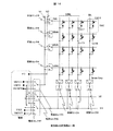
このような動作を実現するための装置構成を図8と図9に示す。本実施例2の半導体記憶装置は、図8に示すような外部からのデータの入力、外部へのデータの出力を行うI/O 1001、情報を記憶するメモリセルアレイ1002、メモリセルアレイへの情報の書込みやメモリセルからの情報の読出しの際にメモリセルアレイに印加する電圧を発生させる少なくとも2種類の電源1003、1004、1005、1006、複数の電源が発生した電圧からメモリセルアレイに印加する電圧を選択する電圧セレクタ1007、メモリセルアレイの複数の配線から電圧を印加する配線を選択する配線セレクタ1008、読出し動作の際にメモリセルアレイの情報を読み出す読み取り部1010、外部からの入力に応じて電源1003、1004、1005、1006、電圧セレクタ1007、配線セレクタ1008、読み取部1010の動作を制御する制御部1009を備える。
An apparatus configuration for realizing such an operation is shown in FIGS. The semiconductor memory device according to the second embodiment has an I /
図9は、図7のメモリセルを複数備えるアレイ構成を示した回路図である。図7のソース線111はUSS、SSを介して複数メモリセルどうしが接続され、図7のビット線もSBL、USBL介して複数メモリセルどうしが接続され、図7のゲート22はSWL、USWLを介して複数メモリセルどうしが接続される。
FIG. 9 is a circuit diagram showing an array configuration including a plurality of memory cells of FIG. The
VSET、VRESET、VON,VREAD、0Vを発生する電源回路と電源電圧を伝達する配線Mn(n=1,2,3,4,5)、電源回路と配線Mnの接続の仕方を選択する電源セレクタ、配線Mnとビット線、ワード線の接続の仕方を選択する配線セレクタ(スイッチ)が有り、メモリアレイの各ビット線、ワード線に適切な電圧を印加してセット動作、リセット動作、読み出し動作を行う。VREADに対して、VSETおよびVRESETは異なる極性とする。 VSET, VRESET, VON, VREAD, power supply circuit for generating 0V, wiring Mn (n = 1, 2, 3, 4, 5) for transmitting power supply voltage, and power supply selector for selecting how to connect the power supply circuit and wiring Mn There is a wiring selector (switch) that selects how to connect the wiring Mn to the bit line and the word line. By applying appropriate voltages to each bit line and word line of the memory array, the set operation, reset operation, and read operation are performed. Do. For VREAD, VSET and VRESET have different polarities.
図9に示すメモリアレイ中から1つのメモリセルSMCを選択して読出しを行なうには、選択セルが接続されているワード線(SWL:選択ワード線)、選択セルが接続されていないワード線(USWL:非選択ワード線)、選択セルが接続されているビット線(SBL:選択ビット線)、選択セルが接続されていないビット線(USBL:非選択ビット線)、選択セルが接続されているソース線(SS:選択ソース線)、選択セルが接続されていないソース線(USS:選択ソース線)に、例えばそれぞれ、VON、0V、VREAD、0V、0V、0Vの電圧を印加する。ゲートに印加される電圧VONは電圧を印加されたトランジスタがオン状態になるように選ぶ。ゲート電圧が0Vではトランジスタがオフ状態になるようにトランジスタを設計する。これらの印加電圧を実現するためには、電源セレクタ2でM4とVREADを接続し、SWLが接続されている配線セレクタでSWLとM2を接続し、USWLが接続されている配線セレクタでUSWLとM3を接続し、SBLが接続されている配線セレクタでSBLとM4を接続し、USBLが接続されている配線セレクタでUSBLとM5を接続し、SSが接続されている配線セレクタでSSとM3を接続し、USSが接続されている配線セレクタでSSとM3を接続すれば良い。
In order to select and read one memory cell SMC from the memory array shown in FIG. 9, the word line to which the selected cell is connected (SWL: selected word line), the word line to which the selected cell is not connected ( USWL: unselected word line), bit line to which the selected cell is connected (SBL: selected bit line), bit line to which the selected cell is not connected (USBL: unselected bit line), and selected cell are connected For example, voltages of VON, 0 V, VREAD, 0 V, 0 V, and 0 V are applied to the source line (SS: selected source line) and the source line (USS: selected source line) not connected to the selected cell, respectively. The voltage VON applied to the gate is selected so that the transistor to which the voltage is applied is turned on. The transistor is designed so that the transistor is turned off when the gate voltage is 0V. In order to realize these applied voltages, M4 and VREAD are connected by the
SWL、USBL、SSに接続されたセル、例えばCell Cではトランジスタはオン状態になるが、SSとUSBLがともに0Vで等電位であるためメモリセルに電流は流れない。USWL、SBL、USSに接続されたセル、例えばCell Bではトランジスタがオフ状態になるのでメモリセルに電流は流れない。USWL、USBL、USSに接続されたセル、例えばCell Dではトランジスタがオフ状態になり、SSとUSBLがともに0Vで等電位であるためメモリセルに電流は流れない。SWL、SBL、SSに接続されたCell A、つまり選択メモリセルSMCだけに図5、図7の方向M2−M1の方向に電流が流れる。読み出し時のSWLの電位VONは例えば2Vとして、トランジスタのオン抵抗を十分小さくする。SBLの電位VREADはSMCの抵抗変化型素子への印加電圧がVreset1の大きさを超えない範囲で大きくする。こうすることで、Ireset1の大きさを超えない範囲のなるべく大きな読み出し電流IREADLを低抵抗状態時のSMCに流すことができる。
IREADHの大きさ<Ic<IREADLの大きさ<Ireset1の大きさ ・・・(11)
の関係が成り立つ範囲でIcを大きくする。抵抗変化型素子の大きなIreset1を活かした大きなIcを用いて読み取り部1010のセンスアンプ(Sense Amp.)で高速に抵抗値を読みだすことができる。
In a cell connected to SWL, USBL, SS, for example, Cell C, the transistor is turned on, but since SS and USBL are both at 0 V and are equipotential, no current flows through the memory cell. In a cell connected to USWL, SBL, USS, for example, Cell B, the transistor is turned off, so that no current flows through the memory cell. In a cell connected to USWL, USBL, and USS, for example, Cell D, the transistor is turned off, and since SS and USBL are both at 0 V and equipotential, no current flows through the memory cell. A current flows only in Cell A connected to SWL, SBL, and SS, that is, in the selected memory cell SMC, in the direction of M2-M1 in FIGS. The potential VON of SWL during reading is set to 2 V, for example, so that the on-resistance of the transistor is sufficiently reduced. The potential VREAD of SBL is increased in a range where the voltage applied to the resistance change element of SMC does not exceed the magnitude of Vreset1. By doing so, it is possible to flow a read current IREADL as large as possible within a range not exceeding the magnitude of Ireset1 to the SMC in the low resistance state.
IREADH size <Ic <IREADL size <Ireset1 size (11)
Ic is increased within a range where the above relationship is satisfied. The resistance value can be read at high speed by the sense amplifier (Sense Amp.) Of the
なお、実際の読み出し動作の際には、図10(a)のように印加電圧を時間変化させ、時刻t4〜t5の間に読み出しを行う。各時刻での電源セレクタ、配線セレクタの接続先を図10(b)のようにすることで図10(a)の電圧印加は実現できる。 In the actual reading operation, the applied voltage is changed with time as shown in FIG. 10A, and reading is performed between times t4 and t5. The voltage application in FIG. 10A can be realized by connecting the power source selector and the wiring selector at each time as shown in FIG.
低抵抗化動作には、図9で、SWL、USWL、SBL、USBL、SS、USSに例えばそれぞれ、VON、0V、0V、VSET、VSET、0Vの電圧を印加する。VSETは式(9)のVset2を越える電圧を用いることができる。たとえば、VON=2.5V、VSET=1.2Vのようにできる。 In the low resistance operation, for example, voltages VON, 0V, 0V, VSET, VSET, and 0V are applied to SWL, USWL, SBL, USBL, SS, and USS, respectively, in FIG. As VSET, a voltage exceeding Vset2 in Expression (9) can be used. For example, VON = 2.5V, VSET = 1.2V.
これを実現するためには、電源セレクタ1でM1とVSETを接続し、電源セレクタ2でM4とVSETを接続し、SWLが接続されている配線セレクタでSWLとM2を接続し、USWLが接続されている配線セレクタでUSWLとM3を接続し、SBLが接続されている配線セレクタでSBLとM5を接続し、USBLが接続されている配線セレクタでUSBLとM4を接続し、SSが接続されている配線セレクタでSSとM1を接続し、USSが接続されている配線セレクタでSSとM3を接続すれば良い。
To achieve this, the
SWL、USBL、SSに接続されたセル、例えばCell Cではトランジスタはオン状態になるが、SSとUSBLがともにVSETで等電位であるためメモリセルに電流は流れない。USWL、SBL、USSに接続されたセル、例えばCell Bではトランジスタがオフ状態になるのでメモリセルに電流は流れない。USWL、USBL、USSに接続されたセル、例えばCell Dではトランジスタがオフ状態になり、SSとUSBLがともにVSETで等電位であるためメモリセルに電流は流れない。結局、SWL、SBL、SSに接続されたCell A、つまり選択メモリセルSMCだけに図5、図7の方向M1−M2の方向にセット電圧が印加され電流が流れ、低抵抗化動作を行うことができる。 In a cell connected to SWL, USBL, SS, for example, Cell C, the transistor is turned on. However, since SS and USBL are both equipotential at VSET, no current flows through the memory cell. In a cell connected to USWL, SBL, USS, for example, Cell B, the transistor is turned off, so that no current flows through the memory cell. In a cell connected to USWL, USBL, and USS, for example, Cell D, the transistor is turned off, and since SS and USBL are both equipotential at VSET, no current flows through the memory cell. Eventually, only the cell A connected to SWL, SBL, SS, that is, the selected memory cell SMC, is applied with a set voltage in the direction of directions M1-M2 in FIGS. Can do.
なお、実際の低抵抗化動作の際には、図11(a)のように印加電圧を時間変化させ、時刻t4〜t5の間に低抵抗化動作を行う。各時刻での電源セレクタ、配線セレクタの接続先を図11(b)のようにすることで図11(a)の電圧印加は実現できる。 In the actual resistance reduction operation, the applied voltage is changed over time as shown in FIG. 11A, and the resistance reduction operation is performed between times t4 and t5. The voltage application in FIG. 11A can be realized by connecting the power source selector and the wiring selector at each time as shown in FIG.
高抵抗化動作には、図9で、SWL、USWL、SBL、USBL、SS、USSに例えばそれぞれ、VON、0V、0V、VRESET、VRESET、0Vの電圧を印加する。たとえば、VON=3V、VRESET=0.7Vとできる。 For the high resistance operation, for example, voltages VON, 0V, 0V, VRESET, VRESET, and 0V are applied to SWL, USWL, SBL, USBL, SS, and USS, respectively, in FIG. For example, VON = 3V and VRESET = 0.7V.
これを実現するためには、電源セレクタ1でM1とVRESETを接続し、電源セレクタ2でM4とVRESETを接続し、SWLが接続されている配線セレクタでSWLとM2を接続し、USWLが接続されている配線セレクタでUSWLとM3を接続し、SBLが接続されている配線セレクタでSBLとM5を接続し、USBLが接続されている配線セレクタでUSBLとM4を接続し、SSが接続されている配線セレクタでSSとM1を接続し、USSが接続されている配線セレクタでSSとM3を接続すれば良い。
To achieve this, the
SWL、USBL、SSに接続されたセル、例えばCell Cではトランジスタはオン状態になるが、SSとUSBLがともにVRESETで等電位であるためメモリセルに電流は流れない。USWL、SBL、USSに接続されたセル、例えばCell Bではトランジスタがオフ状態になるのでメモリセルに電流は流れない。USWL、USBL、USSに接続されたセル、例えばCell Dではトランジスタがオフ状態になり、SSとUSBLがともにVRESETで等電位であるためメモリセルに電流は流れない。結局、SWL、SBL、SSに接続されたCell A、つまり選択メモリセルSMCだけに図5、図7の方向M1−M2の方向にリセット電圧が印加され電流が流れ、高抵抗化動作を行うことができる。 In a cell connected to SWL, USBL, SS, for example, Cell C, the transistor is turned on. However, since SS and USBL are both VRESET and equipotential, no current flows through the memory cell. In a cell connected to USWL, SBL, USS, for example, Cell B, the transistor is turned off, so that no current flows through the memory cell. In cells connected to USWL, USBL, and USS, for example, Cell D, the transistor is turned off, and since SS and USBL are both VRESET and equipotential, no current flows through the memory cell. Eventually, only the cell A connected to SWL, SBL, SS, that is, the selected memory cell SMC, is applied with a reset voltage in the direction of the directions M1-M2 in FIGS. Can do.
なお、実際の低抵抗化動作の際には、図12(a)のように印加電圧を時間変化させ、時刻t4〜t5の間に低抵抗化動作を行う。各時刻での電源セレクタ、配線セレクタの接続先を図12(b)のようにすることで図12(a)の電圧印加は実現できる。 In the actual resistance reduction operation, the applied voltage is changed with time as shown in FIG. 12A, and the resistance reduction operation is performed between times t4 and t5. The voltage application in FIG. 12A can be realized by connecting the power source selector and the wiring selector at each time as shown in FIG.
本発明の実施例2でも実施例1と同様に、従来並みの書換え電流を維持したままでIcを増加させることができる。その結果メモリアレイの読み出し速度を向上することができる。 In the second embodiment of the present invention, as in the first embodiment, Ic can be increased while maintaining the rewrite current as usual. As a result, the reading speed of the memory array can be improved.
本実施例3では、実施例1で用いたノンポーラ型抵抗変化型素子で、ダイオードと組み合わせることでメモリアレイを形成し動作させた。メモリアレイ中の特定の素子を選択して読出し動作、書換え動作を行えるようにするために、各々の抵抗変化型素子と選択ダイオードを図13のように接続し、1つのダイオードと1つの抵抗変化型素子で1つのメモリ素子を形成するようにした。ダイオードを選択素子に用いたメモリアレイは、トランジスタを用いたメモリアレイと比べて微細化に適している。 In Example 3, a memory array was formed and operated by combining the nonpolar variable resistance element used in Example 1 with a diode. In order to select a specific element in the memory array so that a read operation and a rewrite operation can be performed, each resistance variable element and the selection diode are connected as shown in FIG. 13, and one diode and one resistance change are connected. One memory element is formed by the mold element. A memory array using a diode as a selection element is more suitable for miniaturization than a memory array using a transistor.
電極7が仕事関数が小さい金属M1、電極8が仕事関数が大きい金属M2、6が金属酸化物MOとすると、抵抗変化型素子の上部電極7に0V、下部電極8に正電圧を印加する方向が図5の方向M2−M1の方向、下部電極8に0V、上部電極7に正電圧を印加する方向が図5の方向M1−M2の方向となるように抵抗変化型素子を作製できる。
When the
抵抗変化型素子は、たとえば、Vset1、Vreset1、Vset2、Vreset2を、式(7)(8)(9)(10)のようにすることが可能である。 In the variable resistance element, for example, Vset1, Vreset1, Vset2, and Vreset2 can be set as shown in equations (7), (8), (9), and (10).
図13のメモリセルアレイは、金属配線からなるワード線2、ワード線2と接するP型シリコン4、不純物が低濃度のシリコンでダイオードの電界緩和層として機能する11、N型シリコン5、Tiシリサイドなどのバリアメタル10、抵抗変化型素子の下部電極8、抵抗変化型素子6、抵抗変化型素子の上部電極7、ビット線となる金属配線3からなる。
The memory cell array of FIG. 13 includes a
P型シリコン4、不純物が低濃度のシリコン11、N型シリコン5からなるダイオードは整流性を持ち、方向M2−M1が順バイアス方向、方向M1−M2が逆バイアス方向と一致している。なおこれらのシリコン部分は、例えばポリシリコンとすることもできる。ダイオードに順方向電圧を印加した際に十分大きな電流が流れる電圧の大きさVdthはたとえば1.5V、ダイオードの逆バイアス方向の耐圧Vjbはたとえば3Vになるように作製することが可能である。
A diode made of P-
図14はメモリアレイ構成を示した回路図である。VSET、VRESET、VREAD、VSET0、VRESET0、0Vを発生する電源回路と電源電圧を伝達する配線Mn(n=1,2,3,4)、電源回路と配線Mnの接続の仕方を選択する電源セレクタ、配線Mnとビット線、ワード線の接続の仕方を選択する配線セレクタが有り、メモリアレイの各ビット線、ワード線に適切な電圧を印加してセット動作、リセット動作、読み出し動作を行う。 FIG. 14 is a circuit diagram showing a memory array configuration. VSET, VRESET, VREAD, VSET0, VRESET0, a power supply selector that selects a power supply circuit that generates 0V, a wiring Mn (n = 1, 2, 3, 4) that transmits the power supply voltage, and a connection method between the power supply circuit and the wiring Mn There is a wiring selector for selecting how to connect the wiring Mn to the bit line and the word line, and an appropriate voltage is applied to each bit line and word line of the memory array to perform the set operation, reset operation, and read operation.
図14に示すメモリアレイ中から1つのメモリセルSMCを選択して読出しを行なうには、図14で、SWL、USWL、SBL、USBLに、それぞれ、VREAD、0V、0V、VREADの電圧を印加する。 To select and read one memory cell SMC from the memory array shown in FIG. 14, the voltages VREAD, 0V, 0V, and VREAD are applied to SWL, USWL, SBL, and USBL, respectively, in FIG. .
これを実現するためには、図14の電源セレクタ1でM1とVREADを接続し、電源セレクタ2でM3とVREADを接続し、電源セレクタ3でM4と0Vを接続し、SWLが接続されている配線セレクタでSWLとM1を接続し、USWLが接続されている配線セレクタでUSWLとM2を接続し、SBLが接続されている配線セレクタでSBLとM4を接続し、USBLが接続されている配線セレクタでUSBLとM3を接続すれば良い。
In order to realize this, the
SWL、USBLに接続されたセル、例えばCell CではSWLとUSBLがともにVREADで等電位であるためメモリセルに電流は流れない。USWL、SBLに接続されたセル、例えばCell BではUSWL、SBLがともに0Vで等電位であるためメモリセルに電流は流れない。USWL、USBLに接続されたセル、例えばCell Dではダイオードの逆バイアス方向にVREADの電圧が印加される。VREADがダイオードの耐圧Vjbよりも低ければメモリセルに電流は流れない。結局、SWL、SBLに接続されたCell A、つまり選択メモリセルSMCだけに図5、図13の方向M2−M1の方向に電流が流れる。読み出し時のSWL,USBL電位VREADは低抵抗状態のセルが高抵抗化しないこと、つまり抵抗変化型素子への印加電圧がVreset1の大きさを超えない
VREAD < Vreset1の大きさ+Vdth ・・・(12)
の範囲で大きくすることが可能である。CellDなどのUSWL、USBLに接続されたセルのダイオードへの逆方向電圧が耐圧を超えない条件
VREAD < Vjb ・・・(13)
は満たさなくてはならない。
In cells connected to SWL and USBL, for example, Cell C, since SWL and USBL are both VREAD and equipotential, no current flows through the memory cell. In a cell connected to USWL and SBL, for example, Cell B, since USWL and SBL are both 0V and equipotential, no current flows through the memory cell. In a cell connected to USWL and USBL, for example, Cell D, a voltage of VREAD is applied in the reverse bias direction of the diode. If VREAD is lower than the withstand voltage Vjb of the diode, no current flows through the memory cell. Eventually, current flows only in Cell A connected to SWL and SBL, that is, in the selected memory cell SMC, in the direction of M2-M1 in FIGS. The SWL and USBL potential VREAD at the time of reading is such that the cell in the low resistance state does not increase in resistance, that is, the voltage applied to the resistance variable element does not exceed the magnitude of Vreset1 VREAD <the magnitude of Vreset1 + Vdth (12) )
It is possible to increase it within the range. Conditions in which reverse voltage to diode of cell connected to USWL, USBL such as CellD does not exceed withstand voltage VREAD <Vjb (13)
Must be satisfied.
こうすることで、Ireset1の大きさを超えない範囲のなるべく大きな読み出し電流IREADを低抵抗状態時のSMCに流すことができる。
IREADHの大きさ<Ic<IREADLの大きさ<Ireset1の大きさ ・・・(14)
の関係が成り立つ範囲でIcを大きくする。抵抗変化型素子の大きなIreset1を活かした大きなIcを用いることができるので、Sense Amp.で高速に抵抗値を読みだすことができる。
By doing so, a read current IREAD as large as possible within a range not exceeding the magnitude of Ireset1 can be passed through the SMC in the low resistance state.
IREADH size <Ic <IREADL size <Ireset1 size (14)
Ic is increased within a range where the above relationship is satisfied. Since a large Ic utilizing the large Ireset1 of the resistance variable element can be used, Sense Amp. Can read out the resistance value at high speed.
なお、実際の読み出し動作の際には、図15(a)のように印加電圧を時間変化させ、時刻t4〜t5の間に読み出しを行う。各時刻での電源セレクタ、配線セレクタの接続先を図15(b)のようにすることで図15(a)の電圧印加は実現できる。 In the actual reading operation, the applied voltage is changed with time as shown in FIG. 15A, and reading is performed between times t4 and t5. The voltage application of FIG. 15A can be realized by connecting the power source selector and the wiring selector at each time as shown in FIG.
読出し動作のVREADと、Vjb、Vdth、Vreset1の関係を従来動作のVREAD、VRESETの関係と比較して示したのが図16である。式(12)(13)の範囲でなるべく大きいVREADで読出しを行うが、Vjb < Vreset1の大きさ+VdthだとVjbに制限されて、VREADを上げられなくなるので、Vjbは十分大きくなるようにダイオードのデバイス設計をすることが必要である。 FIG. 16 shows the relationship between VREAD in the read operation and Vjb, Vdth, Vreset1 in comparison with the relationship between VREAD and VRESET in the conventional operation. Reading is performed with VREAD as large as possible within the range of Expressions (12) and (13). However, if Vjb <the magnitude of Vreset1 + Vdth, Vjb is limited to Vjb and VREAD cannot be increased. It is necessary to design the device.
低抵抗化動作には、図14で、SWL、USWL、SBL、USBLに例えばそれぞれ、0V、VSET0、VSET、VSET0の電圧を印加する。たとえば、VSET0=2.2V、VSET=4.4Vとできる。SWL、USBLに接続されたセル、例えばCell Cではダイオードの逆バイアス方向に2.2Vの電圧が印加される。耐圧3Vよりも低い電圧がダイオードの逆バイアス方向に印加されるのでメモリセルに電流は流れない。USWL、SBLに接続されたセル、例えばCell Bではダイオードの逆バイアス方向に2.2Vの電圧が印加される。耐圧3Vよりも低い電圧がダイオードの逆バイアス方向に印加されるのでメモリセルに電流は流れない。USWL、USBLに接続されたセル、例えばCell DではUSWL、USBLがともに2.2Vで等電位であるためにメモリセルに電流は流れない。SWL、SBLに接続されたCellA、つまり選択メモリセルSMCでは、ダイオードの耐圧3Vを越える4.4Vの電圧が印加されるので方向M1−M2の方向に電流が流れる。SMCのダイオードに3V、抵抗変化型素子にはVset2の大きさ=1.0Vを越える1.4Vが印加されるので低抵抗化動作を行うことができる。図17(a)のように途中、時刻t1からt2でSBL、USBLを同時に立上げその後時刻t3からt4でUSWLを立ち上げ、t5からt6でSBLを低抵抗化に必要なVSETに立ち上げている。こうすることで、低抵抗化動作の途中で過渡的な電流による非選択セルへの誤書換えを防止できる。VSET0、VSETは抵抗変化型素子のVset2、ダイオードのVjbと、下記の式(15)(16)(17)の関係があれば良い。
VSET0 < Vjb ・・・(15)
0 <VSET−VSET0 < Vjb ・・・(16)
Vjb+Vset2の大きさ < VSET ・・・(17)
なお、実際の低抵抗化動作の際には、図17(a)のように印加電圧を時間変化させ、時刻t6〜t7の間に低抵抗化動作を行う。各時刻での電源セレクタ、配線セレクタの接続先を図17(b)のようにすることで図17(a)の電圧印加は実現できる。
In the low resistance operation, for example, voltages of 0V, VSET0, VSET, and VSET0 are applied to SWL, USWL, SBL, and USBL, respectively, in FIG. For example, VSET0 = 2.2V and VSET = 4.4V. In a cell connected to SWL and USBL, for example, Cell C, a voltage of 2.2 V is applied in the reverse bias direction of the diode. Since a voltage lower than the withstand voltage of 3 V is applied in the reverse bias direction of the diode, no current flows through the memory cell. In a cell connected to USWL and SBL, for example, Cell B, a voltage of 2.2 V is applied in the reverse bias direction of the diode. Since a voltage lower than the withstand voltage of 3 V is applied in the reverse bias direction of the diode, no current flows through the memory cell. In a cell connected to USWL and USBL, for example, Cell D, since USWL and USBL are both equipotential at 2.2 V, no current flows through the memory cell. In CellA connected to SWL and SBL, that is, the selected memory cell SMC, a voltage of 4.4 V exceeding the withstand voltage 3 V of the diode is applied, so that a current flows in the direction of the direction M1-M2. Since 3V is applied to the SMC diode and 1.4V exceeding the magnitude of Vset2 = 1.0V is applied to the resistance variable element, a low resistance operation can be performed. As shown in FIG. 17 (a), SBL and USBL are simultaneously raised from time t1 to t2, and then USWL is raised from time t3 to t4, and SBL is raised to VSET necessary for low resistance from t5 to t6. Yes. By doing so, it is possible to prevent erroneous rewriting to a non-selected cell due to a transient current during the low resistance operation. VSET0 and VSET only need to have the relationship of the following formulas (15), (16), and (17) with Vset2 of the resistance variable element and Vjb of the diode.
VSET0 <Vjb (15)
0 <VSET-VSET0 <Vjb (16)
Size of Vjb + Vset2 <VSET (17)
In the actual resistance reduction operation, the applied voltage is changed with time as shown in FIG. 17A, and the resistance reduction operation is performed between times t6 and t7. The voltage application shown in FIG. 17A can be realized by connecting the power source selector and the wiring selector at each time as shown in FIG.
高抵抗化動作には、図14で、SWL、USWL、SBL、USBLに例えばそれぞれ、0V、VRESET0、VRESET、VRESET0を印加する。たとえば、VRESET0=1.8V、VRESET=3.6Vとできる。SWL、USBLに接続されたセル、例えばCell Cではダイオードの逆バイアス方向に1.8Vの電圧が印加される。耐圧3Vよりも低い電圧がダイオードの逆バイアス方向に印加されるのでメモリセルに電流は流れない。USWL、SBLに接続されたセル、例えばCell Bではダイオードの逆バイアス方向に1.8Vの電圧が印加される。耐圧3 Vよりも低い電圧がダイオードの逆バイアス方向に印加されるのでメモリセルに電流は流れない。USWL、USBLに接続されたセル、例えばCell DではUSWL、USBLがともに1.8Vで等電位であるためにメモリセルに電流は流れない。SWL、SBLに接続されたCell A、つまり選択メモリセルSMCでは、ダイオードの耐圧3 Vを越える3.6Vの電圧が印加されるので方向M1−M2の方向に電流が流れる。抵抗変化型素子にはVreset2の大きさ = 0.5Vを越える0.6Vが印加されるので高抵抗化動作を行うことができる。図18(a)のように低抵抗化動作の場合と同様に、途中、時刻t1からt2でSBL、USBLを同時に立上げその後時刻t3からt4でUSWLを立ち上げ、t5からt6でSBLを高抵抗化に必要なVRESETに立ち上げている。こうすることで、高抵抗化動作の途中で過渡的な電流による非選択セルへの誤書換えを防止できる。VRESET0、VRESETは抵抗変化型素子のVreset2、ダイオードのVjbと、下記の式(18)、(19)、(20)の関係があれば良い。
VRESET0 < Vjb ・・・(18)
0 <VRESET−VRESET0 < Vjb ・・・(19)
Vjb+Vreset2の大きさ < VRESET ・・・(20)
なお、実際の高抵抗化動作の際には、図18(a)のように印加電圧を時間変化させ、時刻t6〜t7の間に高抵抗化動作を行う。各時刻での電源セレクタ、配線セレクタの接続先を図18(b)のようにすることで図18(a)の電圧印加は実現できる。
In the high resistance operation, for example, 0V, VRESET0, VRESET, and VRESET0 are applied to SWL, USWL, SBL, and USBL, respectively, in FIG. For example, VRESET0 = 1.8V and VRESET = 3.6V. In a cell connected to SWL and USBL, for example, Cell C, a voltage of 1.8 V is applied in the reverse bias direction of the diode. Since a voltage lower than the withstand voltage of 3 V is applied in the reverse bias direction of the diode, no current flows through the memory cell. In a cell connected to USWL and SBL, for example, Cell B, a voltage of 1.8 V is applied in the reverse bias direction of the diode. Since a voltage lower than the withstand voltage of 3 V is applied in the reverse bias direction of the diode, no current flows through the memory cell. In cells connected to USWL and USBL, for example, Cell D, since USWL and USBL are both 1.8 V and equipotential, no current flows through the memory cell. In Cell A connected to SWL and SBL, that is, the selected memory cell SMC, a voltage of 3.6 V exceeding the withstand voltage 3 V of the diode is applied, so that a current flows in the direction of M1 to M2. Since the resistance change element is applied with 0.6V exceeding the magnitude of Vreset2 = 0.5V, an operation of increasing resistance can be performed. As in the case of the low resistance operation as shown in FIG. 18A, SBL and USBL are raised at the same time from time t1 to t2, and then the USWL is raised from time t3 to t4, and SBL is raised from t5 to t6. VRESET is required for resistance. By doing so, it is possible to prevent erroneous rewriting to a non-selected cell due to a transient current during the high resistance operation. VRESET0 and VRESET need only have a relationship of Vreset2 of the variable resistance element and Vjb of the diode and the following equations (18), (19), and (20).
VRESET0 <Vjb (18)
0 <VRESET−VRESET0 <Vjb (19)
Size of Vjb + Vreset2 <VRESET (20)
In the actual resistance increasing operation, the applied voltage is changed with time as shown in FIG. 18A, and the resistance increasing operation is performed between times t6 and t7. The voltage application of FIG. 18A can be realized by connecting the power source selector and the wiring selector at each time as shown in FIG.
図17、図18では、SWL、USWL、SBL、USBLに電圧パルスを印加することで低抵抗化動作、高抵抗化動作を行ったが、SBLに対してそれぞれIset2、Ireset2の電流パルスを印加することもできる。 In FIG. 17 and FIG. 18, the low resistance operation and the high resistance operation are performed by applying voltage pulses to SWL, USWL, SBL, and USBL, but current pulses of Iset2 and Ireset2 are applied to SBL, respectively. You can also.
また、実際のデバイスでは、Vreset2、Vset2などにある程度のばらつきがあるので、低抵抗化では式(15)(16)(17)、高抵抗化では式(18)(19)(20)を満たす範囲で、それぞれVSET、VRESETを印加するたびに図15のシーケンスで読出しを行い、低抵抗化動作、高抵抗化動作が完了するまで繰り返すことを行う。 In an actual device, there are some variations in Vreset2, Vset2, etc., so that the equations (15), (16), and (17) are satisfied when the resistance is lowered, and the equations (18), (19), and (20) are satisfied when the resistance is increased. In the range, each time VSET and VRESET are applied, reading is performed in the sequence shown in FIG. 15 and repeated until the low resistance operation and the high resistance operation are completed.
本発明の実施例3でも実施例2と同様に、従来並みの書換え電流を維持したままでIcを増加させることができる。その結果メモリアレイの読み出し速度を向上することができる。 In the third embodiment of the present invention, as in the second embodiment, Ic can be increased while maintaining the conventional rewrite current. As a result, the reading speed of the memory array can be improved.
実施例3では高抵抗化動作と低抵抗化動作をSMCのダイオードの耐圧以上の逆方向電圧印加で行ない読み出しをSMCのダイオードの順方向電圧印加によって行ったが、本実施例4のように読み出し動作をSMCのダイオードの耐圧以上の逆方向電圧印加で行ない高抵抗化動作と低抵抗化動作をSMCのダイオードの順方向電圧印加によって行うこともできる。 In the third embodiment, the high resistance operation and the low resistance operation are performed by applying a reverse voltage higher than the withstand voltage of the SMC diode and reading is performed by applying the forward voltage of the SMC diode. However, the read operation is performed as in the fourth embodiment. The operation can be performed by applying a reverse voltage exceeding the breakdown voltage of the SMC diode, and the high resistance operation and the low resistance operation can be performed by applying the forward voltage of the SMC diode.
実施例1、2の方法で用いたノンポーラ型抵抗変化型素子で、ダイオードと組み合わせることでメモリアレイを形成した。メモリアレイ中の特定の素子を選択して読出し動作、書換え動作を行えるようにするために、各々の抵抗変化型素子と選択ダイオードを図19のように接続し、1つのダイオードと1つの抵抗変化型素子で1つのメモリ素子を形成するようにした。また、その他の方法であっても、図5のような特性をもつノンポーラ型抵抗変化型素子であれば、低抵抗化動作、高抵抗化動作、読出し動作を行うことができ、効果を得ることができる。 A memory array was formed by combining the non-polar variable resistance element used in the methods of Examples 1 and 2 with a diode. In order to select a specific element in the memory array so that a read operation and a rewrite operation can be performed, each resistance change type element and the selection diode are connected as shown in FIG. 19, and one diode and one resistance change are connected. One memory element is formed by the mold element. In addition, even with other methods, if the non-polar variable resistance element having the characteristics shown in FIG. 5 is used, a low resistance operation, a high resistance operation, and a read operation can be performed, and an effect can be obtained. Can do.
電極7が仕事関数が大きい金属M2、電極8が仕事関数が小さい金属M1、6が金属酸化物MOとすると、抵抗変化型素子の上部電極7に0V、下部電極8に正電圧を印加する方向が図5の方向M1−M2の方向、下部電極8に0V、上部電極7に正電圧を印加する方向が図5の方向M2−M1の方向となるように抵抗変化型素子を作製できる。実施例4の場合と逆であることに注意する必要がある。
When the
抵抗変化型素子は、たとえば、Vset1、Vreset1、Vset2、Vreset2を、式(7)、(8)、(9)、(10)のようにすることが可能である。 In the resistance variable element, for example, Vset1, Vreset1, Vset2, and Vreset2 can be changed to equations (7), (8), (9), and (10).
図19のメモリセルアレイは、金属配線からなるワード線2、ワード線2と接するP型シリコン4、不純物が低濃度のシリコンでダイオードの電界緩和層として機能する11、N型シリコン5、Tiシリサイドなどのバリアメタル10、抵抗変化型素子の下部電極8、抵抗変化型素子6、抵抗変化型素子の上部電極7、ビット線となる金属配線3を備える。P型シリコン4、不純物が低濃度のシリコン11、N型シリコン5からなるダイオードは整流性を持ち、方向M2−M1が逆バイアス方向、方向M1−M2が順バイアス方向と一致している。なおこれらのシリコン部分は、例えばポリシリコンとすることもできる。
The memory cell array of FIG. 19 includes a
ダイオードに順方向電圧を印加した際に十分大きな電流が流れる電圧の大きさVdthはたとえば1.5V、ダイオードの逆バイアス方向の耐圧Vjbはたとえば3Vになるように作製することが可能である。 It is possible to produce such that the magnitude Vdth of the voltage through which a sufficiently large current flows when a forward voltage is applied to the diode is 1.5 V, for example, and the withstand voltage Vjb in the reverse bias direction of the diode is 3 V, for example.
図20はメモリアレイ構成を示した回路図である。VSET、VRESET、VREAD、VREAD0、0Vを発生する電源回路と電源電圧を伝達する配線Mn(n=1,2,3,4)、電源回路と配線Mnの接続の仕方を選択する電源セレクタ、配線Mnとビット線、ワード線の接続の仕方を選択する配線セレクタが有り、メモリアレイの各ビット線、ワード線に適切な電圧を印加してセット動作、リセット動作、読み出し動作を行う。 FIG. 20 is a circuit diagram showing a memory array configuration. VSET, VRESET, VREAD, VREAD0, power supply circuit for generating 0V, power supply voltage transmission wiring Mn (n = 1, 2, 3, 4), power supply selector for selecting how to connect the power supply circuit and wiring Mn, wiring There is a wiring selector that selects how to connect Mn to the bit line and the word line, and an appropriate voltage is applied to each bit line and word line of the memory array to perform a set operation, a reset operation, and a read operation.
図20に示すメモリアレイ中から1つのメモリセルSMCを選択して読出しを行なうには、SWL、USWL、SBL、USBLに、例えばそれぞれ、0V、VREAD0、VREAD、VREAD0の電圧を印加する。たとえばVREAD0はVREADと符号が同じで半分の大きさにすることができる。 To select and read one memory cell SMC from the memory array shown in FIG. 20, for example, voltages of 0 V, VREAD0, VREAD, and VREAD0 are applied to SWL, USWL, SBL, and USBL, respectively. For example, VREAD0 has the same sign as VREAD and can be halved.
これを実現するためには、図20の電源セレクタ1でM1とVREAD0を接続し、電源セレクタ2でM3とVREADを接続し、電源セレクタ3でM4とVREAD0を接続し、SWLが接続されている配線セレクタでSWLとM1を接続し、USWLが接続されている配線セレクタでUSWLとM2を接続し、SBLが接続されている配線セレクタでSBLとM3を接続し、USBLが接続されている配線セレクタでUSBLとM4を接続すれば良い。
In order to realize this, M1 and VREAD0 are connected by the
SWL、USBLに接続されたセル、例えばCell Cではダイオードの逆方向に0.5×VREADが印加されるが、耐圧Vjb以下であればメモリセルに電流は流れない。USWL、SBLに接続されたセル、例えばCell BではUSWL、SBLがともにダイオードの逆方向に0.5×VREADが印加されるが、耐圧Vjb以下であればメモリセルに電流は流れない。USWL、USBLに接続されたセル、例えばCell DではUSWL、USBLの電位がともに0.5×VREADで等電位なので電流が流れない。SWL、SBLに接続されたCell A、つまりSMCでは、ダイオードの耐圧3Vを越える電圧が印加できれば方向M2−M1の方向に電流が流れる。SMCへの印加電圧VREADは低抵抗状態のセルが高抵抗化しないこと、つまり抵抗変化型素子への印加電圧がVreset1の大きさを超えず、かつ非選択セルのダイオードへの逆方向電圧が耐圧を超えない
VREAD > Vjb ・・・(21)
VREAD < Vjb + Vreset1の大きさ ・・・(22)
の範囲で大きくすることが可能である。
In a cell connected to SWL and USBL, for example, Cell C, 0.5 × VREAD is applied in the reverse direction of the diode, but no current flows in the memory cell as long as it is lower than the withstand voltage Vjb. In cells connected to USWL and SBL, for example, Cell B, 0.5 × VREAD is applied to both the reverse direction of the diodes in USWL and SBL, but no current flows in the memory cell if the breakdown voltage is Vjb or less. In cells connected to USWL and USBL, for example, Cell D, currents do not flow because the potentials of USWL and USBL are both 0.5 × VREAD and equipotential. In Cell A connected to SWL and SBL, that is, SMC, if a voltage exceeding the withstand voltage of 3V of the diode can be applied, a current flows in the direction of M2-M1. The voltage VREAD applied to the SMC does not increase the resistance of the low resistance state cell, that is, the voltage applied to the resistance variable element does not exceed the magnitude of Vreset1, and the reverse voltage to the diode of the unselected cell is VREAD> Vjb (21)
VREAD <Vjb + Vreset1 size (22)
It is possible to increase it within the range.
Cell CなどのSWL、USBLに接続されたセル、Cell BなどのUSWL、SBLに接続されたセルのダイオードへの逆方向電圧が耐圧を超えない条件、
0.5 ×VREAD < Vjb ・・・(23)
式(21)、(22)、(23)の範囲でなるべく大きなVREADを用いることで、ISET1を超えない範囲のなるべく大きなIcを用いてSense Amp.で高速に抵抗値を読みだすことができる。
SWL such as Cell C, cells connected to USBL, USWL such as Cell B, conditions that the reverse voltage to the diode of the cell connected to SBL does not exceed the breakdown voltage,
0.5 × VREAD <Vjb (23)
By using VREAD as large as possible within the range of the formulas (21), (22), and (23), using the largest Ic within the range not exceeding ISET1, Sense Amp. Can read out the resistance value at high speed.
図21(a)に示すように、途中、時刻t1からt2でSBL、USBLを同時に立上げその後時刻t3からt4でUSWLを立ち上げ、t5からt6でSBLを読出しに必要なVSETSBLに立ち上げている。こうすることで、読出し動作の途中で過渡的な電流が非選択セルへ流れることによる誤読出しを防止できる。 As shown in FIG. 21 (a), SBL and USBL are raised at the same time from time t1 to t2, and then USWL is raised from time t3 to t4, and SBL is raised to VSETSBL necessary for reading from t5 to t6. Yes. By doing so, it is possible to prevent erroneous reading due to a transient current flowing to the non-selected cells during the reading operation.
読出し動作のVREADと、Vjb、Vdth、Vreset1の関係を従来動作のVREAD、VRESETの関係と比較して示したのが図22である。式(21)、(22)、(23)の範囲でなるべく大きいVREADで読出しを行う。 FIG. 22 shows the relationship between VREAD in the read operation and Vjb, Vdth, and Vreset1 in comparison with the relationship between VREAD and VRESET in the conventional operation. Reading is performed with VREAD as large as possible within the range of the equations (21), (22), and (23).
なお、実際の読み出し動作の際には、図21(a)のように印加電圧を時間変化させ、時刻t6〜t7の間に読み出しを行う。各時刻での電源セレクタ、配線セレクタの接続先を図21(b)のようにすることで図21(a)の電圧印加は実現できる。 In the actual reading operation, the applied voltage is changed with time as shown in FIG. 21A, and reading is performed between times t6 and t7. The voltage application in FIG. 21A can be realized by connecting the power source selector and the wiring selector at each time as shown in FIG.
低抵抗化動作には、図20で、SWL、USWL、SBL、USBLに例えばそれぞれ、VSET、0V、0V、VSETの電圧を印加する。 In the low resistance operation, for example, voltages VSET, 0V, 0V, and VSET are applied to SWL, USWL, SBL, and USBL, respectively, in FIG.
たとえば、VSET=2.7Vとできる。SWL、USBLに接続されたセル、例えばCell CではSWL、USBLがともに2.7Vで等電位なので電流は流れない。USWL、SBLに接続されたセル、例えばCell Bでは、USWL、SBLがともに0Vで等電位なので電流は流れない。 For example, VSET = 2.7V. In a cell connected to SWL and USBL, for example, Cell C, since SWL and USBL are both 2.7 V and equipotential, no current flows. In a cell connected to USWL and SBL, for example, Cell B, no current flows because USWL and SBL are both 0 V and equipotential.
USWL、USBLに接続されたセル、例えばCell Dではメモリセルのダイオードに2.7Vの逆方向電圧が印加されるが、耐圧3V以下なので電流は流れない。SWL、SBLに接続されたCell A、つまりSMCでは、ダイオードの順方向に2.7Vが印加されるので方向M1−M2の方向に電流が流れる。ダイオードにはVdth=1.5Vが印加され、抵抗変化型素子にはVset2の大きさ=1.0Vを越える1.2Vが印加されるので低抵抗化動作を行うことができる。 In cells connected to USWL and USBL, for example, Cell D, a reverse voltage of 2.7 V is applied to the diode of the memory cell, but no current flows because the withstand voltage is 3 V or less. In Cell A connected to SWL and SBL, that is, SMC, 2.7 V is applied in the forward direction of the diode, so that a current flows in the direction of direction M1-M2. Since Vdth = 1.5V is applied to the diode and 1.2V exceeding the magnitude of Vset2 = 1.0V is applied to the resistance variable element, a low resistance operation can be performed.
VSETは抵抗変化型素子のVset2、ダイオードのVjb、Vdthと、下記の式(24)、(25)の関係があれば良い。
VSET < Vjb ・・・(24)
Vdth+Vset2の大きさ < VSET ・・・(25)
なお、実際の低抵抗化動作の際には、図23(a)のように印加電圧を時間変化させ、時刻t4〜t5の間に低抵抗化動作を行う。各時刻での電源セレクタ、配線セレクタの接続先を図23(b)のようにすることで図23(a)の電圧印加は実現できる。
VSET only needs to have a relationship of Vset2 of the resistance variable element, Vjb and Vdth of the diode, and the following expressions (24) and (25).
VSET <Vjb (24)
Size of Vdth + Vset2 <VSET (25)
In the actual low resistance operation, the applied voltage is changed with time as shown in FIG. 23A, and the low resistance operation is performed between times t4 and t5. The voltage application in FIG. 23A can be realized by connecting the power supply selector and the wiring selector at each time as shown in FIG.
高抵抗化動作には、図20で、SWL、USWL、SBL、USBLに例えばそれぞれ、VRESET、0V、0V、VRESETの電圧を印加する。たとえば、VRESET=2.2Vとできる。SWL、USBLに接続されたセル、例えばCell CではSWL、USBLがともに2.2Vで等電位なので電流は流れない。USWL、SBLに接続されたセル、例えばCell Bでは、USWL、SBLがともに0Vで等電位なので電流は流れない。 In the high resistance operation, for example, voltages VRESET, 0V, 0V, and VRESET are applied to SWL, USWL, SBL, and USBL, respectively, in FIG. For example, VRESET = 2.2V. In cells connected to SWL and USBL, for example, Cell C, SWL and USBL are both 2.2 V and equipotential, so no current flows. In a cell connected to USWL and SBL, for example, Cell B, no current flows because USWL and SBL are both 0 V and equipotential.
USWL、USBLに接続されたセル、例えばCell Dではメモリセルのダイオードに2.2Vの逆方向電圧が印加されるが、耐圧3V以下なので電流は流れない。SWL、SBLに接続されたCell A、つまりSMCでは、ダイオードの順方向に2.2Vが印加されるので方向M1−M2の方向に電流が流れる。ダイオードにはVdth=1.5Vが印加され、抵抗変化型素子にはVreset2の大きさ=0.5Vを越える0.7Vが印加されるので高抵抗化動作を行うことができる。 In cells connected to USWL and USBL, for example, Cell D, a reverse voltage of 2.2 V is applied to the diode of the memory cell, but no current flows because the withstand voltage is 3 V or less. In Cell A connected to SWL and SBL, that is, SMC, since 2.2 V is applied in the forward direction of the diode, a current flows in the direction of direction M1-M2. Since Vdth = 1.5V is applied to the diode and 0.7V exceeding the magnitude of Vreset2 = 0.5V is applied to the resistance variable element, a high resistance operation can be performed.
VRESETは抵抗変化型素子のVreset2、ダイオードのVjb、Vdthと、下記の式(26)、(27)の関係があれば良い。
VRESET < Vjb ・・・(26)
Vdth+Vreset2の大きさ < VRESET ・・・(27)
なお、実際の高抵抗化動作の際には、図24(a)のように印加電圧を時間変化させ、時刻t4〜t5の間に高抵抗化動作を行う。各時刻での電源セレクタ、配線セレクタの接続先を図24(b)のようにすることで図24(a)の電圧印加は実現できる。
VRESET only needs to have a relationship represented by the following expressions (26) and (27) with Vreset2 of the resistance variable element, Vjb and Vdth of the diode.
VRESET <Vjb (26)
Size of Vdth + Vreset2 <VRESET (27)
In the actual resistance increasing operation, the applied voltage is changed with time as shown in FIG. 24A, and the resistance increasing operation is performed between times t4 and t5. The voltage application in FIG. 24A can be realized by connecting the power source selector and the wiring selector at each time as shown in FIG.
また、実際のデバイスでは、Vreset2、Vset2などにある程度のばらつきがあるので、低抵抗化では式(24)、(25)、高抵抗化では式(26)、(27)を満たす範囲で、それぞれVSET、VRESETを印加するたびに図21のシーケンスで読出しを行い、低抵抗化動作、高抵抗化動作が完了するまで繰り返すことを行う。 In an actual device, there are some variations in Vreset2, Vset2, etc., so that in the range satisfying formulas (24) and (25) for low resistance and formulas (26) and (27) for high resistance, Each time VSET and VRESET are applied, reading is performed in the sequence shown in FIG. 21 and is repeated until the low resistance operation and the high resistance operation are completed.
本発明の実施例4でも実施例3と同様に、従来並みの書換え電流を維持したままでIcを増加させることができる。その結果メモリアレイの読み出し速度を向上することができる。 In the fourth embodiment of the present invention, as in the third embodiment, Ic can be increased while maintaining the rewrite current as in the conventional case. As a result, the reading speed of the memory array can be improved.
実施例3では、低抵抗化動作、高抵抗化動作時に、ダイオードの耐圧以上の電圧を印加して動作させている。しかし、ダイオードに接合耐圧以上の電圧を印加すると急激に電流が流れる。 In the third embodiment, a voltage higher than the withstand voltage of the diode is applied during the low resistance operation and the high resistance operation. However, when a voltage higher than the junction breakdown voltage is applied to the diode, a current flows rapidly.
高抵抗化動作の場合には、メモリセルへの印加電圧がVreset2の大きさ+Vjbになると、抵抗変化型素子の抵抗は高抵抗化する。抵抗変化型素子に印加される電圧は、高抵抗化前はVreset2だったのが高抵抗化後ではVreset2の大きさより大きな値に変化する 。これに伴い、ダイオードへの印加電圧は、高抵抗化前はVjbだったのが、Vjbより小さな値に変化する。ダイオードへの印加電圧がVjbより小さくなるので自動的に、高抵抗化後にはメモリセルに流れる電流が非常に小さくなる。ただし、メモリセルへの印加電圧がVset2の大きさ+Vjbを越えると再び低抵抗化動作が生じてしまうので高抵抗化動作時のメモリセル印加電圧は、Vreset2の大きさ+Vjb以上でかつVset2の大きさ+Vjbより小さくしなくてはならない。 In the case of the high resistance operation, when the voltage applied to the memory cell becomes the magnitude of Vreset2 + Vjb, the resistance of the resistance variable element increases. The voltage applied to the resistance variable element was Vreset2 before the increase in resistance, but changes to a value larger than the magnitude of Vreset2 after the increase in resistance. Accordingly, the voltage applied to the diode changes from Vjb before the increase in resistance to a value smaller than Vjb. Since the voltage applied to the diode becomes smaller than Vjb, the current flowing through the memory cell becomes very small automatically after increasing the resistance. However, when the applied voltage to the memory cell exceeds the magnitude of Vset2 + Vjb, the resistance reduction operation occurs again. Therefore, the voltage applied to the memory cell during the high resistance operation is greater than the magnitude of Vreset2 + Vjb and the magnitude of Vset2. Must be smaller than + Vjb.
低抵抗化動作の場合には、メモリセルへの印加電圧がVset2の大きさ+Vjbになると、抵抗変化型素子の抵抗は低抵抗化する。抵抗変化型素子に印加される電圧は、低抵抗化前はVset2の大きさだったのが高抵抗化後ではVset2の大きさより小さな値に変化する 。これに伴い、ダイオードへの印加電圧は、高抵抗化前はVjbだったのが、Vjbより大きな値に変化する。ダイオードへの印加電圧がVjbより大きくなるので、低抵抗化後にはメモリセルに流れる電流は激増し、ジュール熱による発熱により、ダイオードやメモリ素子が破壊される場合がある。 In the case of the low resistance operation, when the voltage applied to the memory cell becomes the magnitude of Vset2 + Vjb, the resistance of the resistance variable element decreases. The voltage applied to the resistance variable element is the value of Vset2 before the resistance is lowered, but changes to a value smaller than the value of Vset2 after the resistance is increased. Accordingly, the voltage applied to the diode changes from Vjb before the increase in resistance to a value larger than Vjb. Since the voltage applied to the diode becomes higher than Vjb, the current flowing through the memory cell increases dramatically after the resistance is lowered, and the diode and the memory element may be destroyed due to heat generated by Joule heat.
低抵抗化動作時の過渡的な高電流を防止するために、図25のようにワード線、ビット線とメモリアレイ外部の電源との間にワード線選択トランジスタSTTWL,ビット線選択トランジスタSTTBLを設置した。 In order to prevent a transient high current during the low resistance operation, a word line selection transistor STTWL and a bit line selection transistor STTBL are installed between the word line and bit line and the power supply outside the memory array as shown in FIG. did.
電源回路、電源セレクタ、配線セレクタは図示しないが、実施例3すなわち図14と同じ構成であり、SWL、USWLと配線セレクタとがSTTWL,SBL,USBLと配線セレクタとがSTTBLを介して接続されていることが実施例3と本実施例5が異なる点である。 Although the power supply circuit, power supply selector, and wiring selector are not shown, they have the same configuration as that of the third embodiment, that is, FIG. 14, and SWL, USWL and the wiring selector are connected to STTWL, SBL, USBL and the wiring selector through STTBL This is the difference between the third embodiment and the fifth embodiment.
高抵抗化動作、低抵抗化動作、読出し動作でのSWL、USWL、SBL、USBL電位は実施例3と同様である。 The SWL, USWL, SBL, and USBL potentials in the high resistance operation, the low resistance operation, and the read operation are the same as those in the third embodiment.
低抵抗化動作時にSWL−SBL間に印加される電圧VSETは、STTWL、SMCのダイオード、SMCの抵抗変化型素子、STTBLの直列構造に印加される。STTWL、STTBLの飽和電流をたとえばIreset2の2倍の大きさ程度になるようにSTTWL、STTBL電圧を設定すると、低抵抗化動作時にSMCのダイオードがVjb以上の電圧印加で低抵抗化し、SMCの抵抗変化型素子が低抵抗化してもSTTWL、STTBLで電流が制限されるので発熱によるダイオードやメモリ素子が破壊を避けることができる。 The voltage VSET applied between SWL and SBL during the low resistance operation is applied to the serial structure of STTWL, SMC diode, SMC resistance change element, and STTBL. If the STTWL and STTBL voltages are set so that the saturation current of STTWL and STTBL is, for example, about twice as large as Ireset2, the SMC diode becomes low resistance by applying a voltage of Vjb or more during the low resistance operation, and the SMC resistance Even if the resistance of the variable element is lowered, the current is limited by STTWL and STTBL, so that the diode and the memory element due to heat generation can be prevented from being destroyed.
高抵抗化動作、読出し動作の際には、STTWL、STTBLの飽和電流がIreset2の大きさと比較して十分に大きくし、かつSTTWL、STTBLでの電圧降下が十分小さくなるように、STTWL、STTBLへの印加電圧を大きくする。 During the high resistance operation and read operation, the saturation current of STTWL and STTBL is sufficiently larger than the magnitude of Ireset2, and the voltage drop at STTWL and STTBL is sufficiently reduced to STTWL and STTBL. Increase the applied voltage.
本発明の実施例5でも実施例3と同様に、従来並みの書換え電流を維持したままでIcを増加させることができる。その結果メモリアレイの読み出し速度を向上することができる。 In the fifth embodiment of the present invention, as in the third embodiment, Ic can be increased while maintaining the rewrite current as in the conventional case. As a result, the reading speed of the memory array can be improved.
本発明の不揮発性半導体記憶装置は、携帯型パーソナルコンピュータやデジタルスチルカメラ等の小型携帯情報機器用記憶装置などに用いて好適なものである。 The nonvolatile semiconductor memory device of the present invention is suitable for use in a memory device for small portable information devices such as a portable personal computer and a digital still camera.
1・・・半導体基板(シリコン基板)、
2・・・ワード線、または選択トランジスタのゲート
3・・・ビット線
4・・・p型シリコン
5・・・n型シリコン
6・・・金属酸化物などの記憶材料
7・・・抵抗変化型素子の上部電極
8・・・抵抗変化型素子の下部電極
10・・・n型シリコン界面のバリアメタル、またはシリサイド
11・・・不純物が低濃度のシリコン、ダイオードの電界緩和層
21・・・ゲート絶縁膜
22・・・ゲート電極
23・・・拡散層
101・・・チャネル
111・・・ソース線
112、113・・・電極
HRS・・・高抵抗状態
LRS・・・低抵抗状態
M1・・・仕事関数が小さい金属
M2・・・仕事関数が大きい金属
MO・・・金属酸化物
VB・・・価電子帯
CB・・・伝導帯
ΦB1、ΦB2・・・バリア高さ
EF・・・フェルミ準位
V1・・・第1電源
V2・・・第2電源
SWL・・・選択ワード線
USWL・・・非選択ワード線
SBL・・・選択ビット線
USBL・・・非選択ビット線
SS・・・選択ソース線
USS・・・非選択ソース線
SMC・・・選択メモリセル
CellA・・・選択ワード線、選択ビット線に接続されたメモリセル
CellB・・・非選択ワード線、選択ビット線に接続されたメモリセル
CellC・・・選択ワード線、非選択ビット線に接続されたメモリセル
CellD・・・非選択ワード線、非選択ビット線に接続されたメモリセル
Sense Amp.・・・センスアンプ
Vset、Vset1、Vset2・・・抵抗変化型素子の低抵抗化電圧
Vreset、Vreset1、Vreset2・・・抵抗変化型素子の高抵抗化電圧
Iset、Iset1、Iset2・・・抵抗変化型素子の低抵抗化電流
Ireset,Ireset1、Ireset2・・・抵抗変化型素子の高抵抗化電流
Vjb・・・ダイオードの逆バイアス耐圧 (降伏電圧)
VREAD・・・読み出し時のメモリセル印加電圧
VSET・・・低抵抗化動作時のメモリセル印加電圧
VRESET・・・高抵抗化動作時のメモリセル印加電圧
VSET0、VRESET0、VREAD0・・・電源電圧
IREAD・・・読み出し時センスアンプ電流
IREADL・・・低抵抗状態の抵抗変化型素子に流れる電流
IREADH・・・高抵抗状態の抵抗変化型素子に流れる電流
Ic・・・読出し動作の際に高抵抗状態と低抵抗状態を区別する電流レベル
Icf・・・大容量フラッシュメモリの高閾値状態と低閾値状態を区別する電流レベル
VON・・・選択素子トランジスタのチャネルをオン状態にするゲート電圧
方向M2−M1・・・抵抗変化型素子の電圧印加、電流を流す方向で高抵抗化電流が大きい方向
方向M1−M2・・・抵抗変化型素子の電圧印加、電流を流す方向で高抵抗化電流が小さい方向
STTWL・・・ワード線と外部電源を接続するトランジスタ
STTBL・・・ビット線と外部電源を接続するトランジスタ
t1、t2、t3、t4、t5、t6、t7、t8、t9、t10、t11、t12、t13・・・時刻
1 ... Semiconductor substrate (silicon substrate),
2 ... Word line or
VREAD: Memory cell applied voltage VSET at read time ... Memory cell applied voltage VRESET at low resistance operation ... Memory cell applied voltage VSET0, VRESET0, VREAD0 ... Power supply voltage IREAD at high resistance operation・ ・ ・ Read sense amplifier current IREADL ・ ・ ・ Current flowing through resistance change element in low resistance state IREADH ・ ・ ・ Current Ic flowing through resistance change element in high resistance state ・ ・ ・ High resistance state during read operation Current level Icf distinguishing between low resistance state and low resistance state Current level VON distinguishing between high threshold state and low threshold state of large-capacity flash memory Gate voltage direction M2-M1 for turning on channel of selected element transistor ... Direction M1-M in the direction in which high resistance current is applied in the direction in which voltage is applied to the variable resistance element and the current flows. ... Voltage application of resistance change type element, direction of increasing current in the direction of flowing current STTWL ... Transistor STTBL for connecting the word line and external power supply ... Transistor t1 for connecting the bit line and external power supply , T2, t3, t4, t5, t6, t7, t8, t9, t10, t11, t12, t13 ... time
Claims (15)
前記第1電源と極性が同じで、かつ前記第1電源よりも出力電圧が高い第2電源と、
前記第1電源と極性が反対で、かつ前記第2電源の出力電圧の絶対値よりも出力電圧が高い第3電源と、
抵抗変化型素子とを有し、
前記抵抗変化型素子は、
第1電極と、
前記第1電極に接続されている、金属酸化物を含む記録層と、
前記記録層に接続されている第2電極とを有し、
前記第2電極の仕事関数が、前記第1電極の仕事関数よりも大きく、
前記第1電極から前記第2電極の方向に電流が流れるように前記抵抗変化型素子に前記第1電源の出力電圧を印加することで、前記抵抗変化型素子の抵抗値を上昇させ、前記第1電極から前記第2電極の方向に電流が流れるように前記抵抗変化型素子に前記第2電源の出力電圧を印加することで、前記抵抗変化型素子の抵抗値を下降させることでデータを書き換え、
前記第2電極から前記第1電極の方向に電流が流れるように前記抵抗変化型素子に前記第3電源の出力電圧を印加することでデータの読み出しを行うことを特徴とする半導体記憶装置。 A first power source;
A second power supply having the same polarity as the first power supply and a higher output voltage than the first power supply;
A third power source having a polarity opposite to that of the first power source and having an output voltage higher than an absolute value of an output voltage of the second power source;
A variable resistance element;
The resistance variable element is:
A first electrode;
A recording layer containing a metal oxide connected to the first electrode;
A second electrode connected to the recording layer,
The work function of the second electrode is greater than the work function of the first electrode;
By applying an output voltage of the first power source to the variable resistance element so that a current flows from the first electrode to the second electrode, the resistance value of the variable resistance element is increased, Data is rewritten by decreasing the resistance value of the resistance variable element by applying the output voltage of the second power source to the resistance variable element so that a current flows from one electrode to the second electrode. ,
2. A semiconductor memory device, wherein data is read by applying an output voltage of the third power source to the resistance variable element so that a current flows from the second electrode to the first electrode.
前記金属酸化物は酸化ニッケルであることを特徴とする半導体記憶装置。 The semiconductor memory device according to claim 1,
A semiconductor memory device, wherein the metal oxide is nickel oxide.
前記金属酸化物は酸化チタンであることを特徴とする半導体記憶装置。 The semiconductor memory device according to claim 1,
A semiconductor memory device, wherein the metal oxide is titanium oxide.
前記第1電極はニッケルを含み、
前記第2電極は白金を含むことを特徴とする半導体記憶装置。 The semiconductor memory device according to claim 2,
The first electrode includes nickel;
The semiconductor memory device, wherein the second electrode contains platinum.
前記記録層の前記第2電極近傍の前記金属酸化物のキャリア濃度が、前記第1電極近傍の前記金属酸化物のキャリア濃度よりも高いことを特徴とする半導体記憶装置。 The semiconductor memory device according to claim 1,
A semiconductor memory device, wherein a carrier concentration of the metal oxide in the vicinity of the second electrode of the recording layer is higher than a carrier concentration of the metal oxide in the vicinity of the first electrode.
前記第2電極と前記記録層との接触面積が、前記第1電極と前記記録層との接触面積よりも小さいことを特徴とする半導体記憶装置。 The semiconductor memory device according to claim 1,
A semiconductor memory device, wherein a contact area between the second electrode and the recording layer is smaller than a contact area between the first electrode and the recording layer.
前記第1電極に接続されている、金属酸化物を含む記録層と、
前記記録層に接続されている第2電極とを有し、
前記記録層の前記第2電極近傍の前記金属酸化物のキャリア濃度が、前記第1電極近傍の前記金属酸化物のキャリア濃度よりも高いことを特徴とする半導体記憶装置。 A first electrode;
A recording layer containing a metal oxide connected to the first electrode;
A second electrode connected to the recording layer,
A semiconductor memory device, wherein a carrier concentration of the metal oxide in the vicinity of the second electrode of the recording layer is higher than a carrier concentration of the metal oxide in the vicinity of the first electrode.
前記金属酸化物は酸化ニッケルであることを特徴とする半導体記憶装置。 The semiconductor memory device according to claim 7,
A semiconductor memory device, wherein the metal oxide is nickel oxide.
前記金属酸化物は酸化チタンであることを特徴とする半導体記憶装置。 The semiconductor memory device according to claim 7,
A semiconductor memory device, wherein the metal oxide is titanium oxide.
前記第1電極はニッケルを含み、
前記第2電極は白金を含むことを特徴とする半導体記憶装置。 The semiconductor memory device according to claim 8.
The first electrode includes nickel;
The semiconductor memory device, wherein the second electrode contains platinum.
前記第2電極と前記記録層との接触面積が、前記第1電極と前記記録層との接触面積よりも小さいことを特徴とする半導体記憶装置。 The semiconductor memory device according to claim 7,
A semiconductor memory device, wherein a contact area between the second electrode and the recording layer is smaller than a contact area between the first electrode and the recording layer.
前記第1電極に接続されている、金属酸化物を含む記録層と、
前記記録層に接続されている第2電極とを有し、
前記第2電極と前記記録層との接触面積が、前記第1電極と前記記録層との接触面積よりも小さいことを特徴とする半導体記憶装置。 A first electrode;
A recording layer containing a metal oxide connected to the first electrode;
A second electrode connected to the recording layer,
A semiconductor memory device, wherein a contact area between the second electrode and the recording layer is smaller than a contact area between the first electrode and the recording layer.
前記金属酸化物は酸化ニッケルであることを特徴とする半導体記憶装置。 The semiconductor memory device according to claim 12,
A semiconductor memory device, wherein the metal oxide is nickel oxide.
前記金属酸化物は酸化チタンであることを特徴とする半導体記憶装置。 The semiconductor memory device according to claim 12,
A semiconductor memory device, wherein the metal oxide is titanium oxide.
前記第1電極はニッケルを含み、
前記第2電極は白金を含むことを特徴とする半導体記憶装置。 The semiconductor memory device according to claim 13.
The first electrode includes nickel;
The semiconductor memory device, wherein the second electrode contains platinum.
Priority Applications (1)
| Application Number | Priority Date | Filing Date | Title |
|---|---|---|---|
| JP2009173843A JP2011029418A (en) | 2009-07-27 | 2009-07-27 | Semiconductor memory device |
Applications Claiming Priority (1)
| Application Number | Priority Date | Filing Date | Title |
|---|---|---|---|
| JP2009173843A JP2011029418A (en) | 2009-07-27 | 2009-07-27 | Semiconductor memory device |
Publications (1)
| Publication Number | Publication Date |
|---|---|
| JP2011029418A true JP2011029418A (en) | 2011-02-10 |
Family
ID=43637823
Family Applications (1)
| Application Number | Title | Priority Date | Filing Date |
|---|---|---|---|
| JP2009173843A Pending JP2011029418A (en) | 2009-07-27 | 2009-07-27 | Semiconductor memory device |
Country Status (1)
| Country | Link |
|---|---|
| JP (1) | JP2011029418A (en) |
Cited By (1)
| Publication number | Priority date | Publication date | Assignee | Title |
|---|---|---|---|---|
| KR101934013B1 (en) * | 2012-03-27 | 2018-12-31 | 에스케이하이닉스 주식회사 | Resistance variable memory device |
-
2009
- 2009-07-27 JP JP2009173843A patent/JP2011029418A/en active Pending
Cited By (1)
| Publication number | Priority date | Publication date | Assignee | Title |
|---|---|---|---|---|
| KR101934013B1 (en) * | 2012-03-27 | 2018-12-31 | 에스케이하이닉스 주식회사 | Resistance variable memory device |
Similar Documents
| Publication | Publication Date | Title |
|---|---|---|
| US8351241B2 (en) | Rectification element and method for resistive switching for non volatile memory device | |
| US7539040B2 (en) | Nonvolatile semiconductor memory device | |
| US7952909B2 (en) | Nonvolatile semiconductor memory device | |
| CN100483542C (en) | Nonvolatile memory cell and non-volatile semiconductor memory device | |
| US7433222B2 (en) | Nonvolatile semiconductor memory device | |
| US8139392B2 (en) | Nonvolatile semiconductor memory device and writing method of the same | |
| KR101744757B1 (en) | Variable resistance element, semiconductor device including the variable resistance element, and method of operation the semiconductor device | |
| US8957399B2 (en) | Nonvolatile memory element and nonvolatile memory device | |
| US8912517B2 (en) | Resistive switching memory | |
| JP5490961B2 (en) | Nonvolatile memory element driving method and nonvolatile memory device | |
| KR20170134381A (en) | Switch element and storage device | |
| KR20110099800A (en) | Memory cell having dielectric memory element | |
| US10832771B2 (en) | Semiconductor memory device | |
| CN111145811B (en) | Resistive random access memory array, operation method thereof and resistive random access memory circuit | |
| CN111179991B (en) | Resistive random access memory array, operation method thereof and resistive random access memory circuit | |
| CN111091858B (en) | Operation method of resistive random access memory array | |
| KR20140047732A (en) | Circuit and method for reading a resistive switching device in an array | |
| US20140085964A1 (en) | Semiconductor storage device | |
| US20220336012A1 (en) | Semiconductor memory devices with differential threshold voltages | |
| JP2011029418A (en) | Semiconductor memory device | |
| JP2015018994A (en) | Nonvolatile semiconductor storage device | |
| US10720576B2 (en) | Semiconductor device | |
| JP2017168643A (en) | Variable-resistance element, nonvolatile storage, and programmable logic device |