JP2011002644A - Display particle for image display and image display - Google Patents
Display particle for image display and image display Download PDFInfo
- Publication number
- JP2011002644A JP2011002644A JP2009145421A JP2009145421A JP2011002644A JP 2011002644 A JP2011002644 A JP 2011002644A JP 2009145421 A JP2009145421 A JP 2009145421A JP 2009145421 A JP2009145421 A JP 2009145421A JP 2011002644 A JP2011002644 A JP 2011002644A
- Authority
- JP
- Japan
- Prior art keywords
- particles
- display
- image display
- metal oxide
- compound
- Prior art date
- Legal status (The legal status is an assumption and is not a legal conclusion. Google has not performed a legal analysis and makes no representation as to the accuracy of the status listed.)
- Pending
Links
Images


Classifications
-
- G—PHYSICS
- G02—OPTICS
- G02F—OPTICAL DEVICES OR ARRANGEMENTS FOR THE CONTROL OF LIGHT BY MODIFICATION OF THE OPTICAL PROPERTIES OF THE MEDIA OF THE ELEMENTS INVOLVED THEREIN; NON-LINEAR OPTICS; FREQUENCY-CHANGING OF LIGHT; OPTICAL LOGIC ELEMENTS; OPTICAL ANALOGUE/DIGITAL CONVERTERS
- G02F1/00—Devices or arrangements for the control of the intensity, colour, phase, polarisation or direction of light arriving from an independent light source, e.g. switching, gating or modulating; Non-linear optics
- G02F1/01—Devices or arrangements for the control of the intensity, colour, phase, polarisation or direction of light arriving from an independent light source, e.g. switching, gating or modulating; Non-linear optics for the control of the intensity, phase, polarisation or colour
- G02F1/165—Devices or arrangements for the control of the intensity, colour, phase, polarisation or direction of light arriving from an independent light source, e.g. switching, gating or modulating; Non-linear optics for the control of the intensity, phase, polarisation or colour based on translational movement of particles in a fluid under the influence of an applied field
- G02F1/166—Devices or arrangements for the control of the intensity, colour, phase, polarisation or direction of light arriving from an independent light source, e.g. switching, gating or modulating; Non-linear optics for the control of the intensity, phase, polarisation or colour based on translational movement of particles in a fluid under the influence of an applied field characterised by the electro-optical or magneto-optical effect
- G02F1/167—Devices or arrangements for the control of the intensity, colour, phase, polarisation or direction of light arriving from an independent light source, e.g. switching, gating or modulating; Non-linear optics for the control of the intensity, phase, polarisation or colour based on translational movement of particles in a fluid under the influence of an applied field characterised by the electro-optical or magneto-optical effect by electrophoresis
-
- G—PHYSICS
- G02—OPTICS
- G02F—OPTICAL DEVICES OR ARRANGEMENTS FOR THE CONTROL OF LIGHT BY MODIFICATION OF THE OPTICAL PROPERTIES OF THE MEDIA OF THE ELEMENTS INVOLVED THEREIN; NON-LINEAR OPTICS; FREQUENCY-CHANGING OF LIGHT; OPTICAL LOGIC ELEMENTS; OPTICAL ANALOGUE/DIGITAL CONVERTERS
- G02F1/00—Devices or arrangements for the control of the intensity, colour, phase, polarisation or direction of light arriving from an independent light source, e.g. switching, gating or modulating; Non-linear optics
- G02F1/01—Devices or arrangements for the control of the intensity, colour, phase, polarisation or direction of light arriving from an independent light source, e.g. switching, gating or modulating; Non-linear optics for the control of the intensity, phase, polarisation or colour
- G02F1/165—Devices or arrangements for the control of the intensity, colour, phase, polarisation or direction of light arriving from an independent light source, e.g. switching, gating or modulating; Non-linear optics for the control of the intensity, phase, polarisation or colour based on translational movement of particles in a fluid under the influence of an applied field
- G02F1/1675—Constructional details
- G02F2001/1678—Constructional details characterised by the composition or particle type
Abstract
Description
表示粒子を電界中で移動させることにより、画像の表示および消去を繰り返し実行できる画像表示装置および該画像表示装置に用いられる表示粒子に関する。 The present invention relates to an image display device capable of repeatedly executing display and erasing of an image by moving the display particles in an electric field, and a display particle used in the image display device.
従来より、表示粒子を気相中で移動させて画像を表示する画像表示装置が知られている。画像表示装置は、少なくとも一方が透明な2枚の基板間に表示粒子が粉体形態で封入されてなり、該基板間に電界を発生させることによって、表示粒子を一方の基板に移動・付着させて画像を表示するものである。そのような画像表示装置の駆動の際には、基板間に電圧を印加して電界を発生させ、当該電界方向に沿って表示粒子が移動するため、電界方向を適宜選択することによって画像の表示および消去を繰り返し実行できる。そのため、画像表示装置には、表示粒子と基板間における表示粒子接触面との付着力を低減することが求められていた。 2. Description of the Related Art Conventionally, an image display device that displays an image by moving display particles in a gas phase is known. In an image display device, display particles are sealed in a powder form between two substrates, at least one of which is transparent, and an electric field is generated between the substrates to move and attach the display particles to one substrate. Display an image. When driving such an image display device, an electric field is generated by applying a voltage between the substrates, and the display particles move along the electric field direction. Therefore, an image can be displayed by appropriately selecting the electric field direction. And erasure can be executed repeatedly. Therefore, the image display device has been required to reduce the adhesion between the display particles and the display particle contact surface between the substrates.
画像表示装置に使用される表示粒子としては、結着樹脂および着色剤を含有する母体粒子の表面に疎水性シリカや疎水性チタニアなどの無機微粒子をヘンシェルミキサー等による乾式混合法にて被覆したものが知られている(特許文献1)。しかしながら、上述した乾式混合法では、完全に母体粒子表面を覆うことができないので、微粒子による付着力低減効果が十分に発揮できない。そのため、繰り返しの駆動時において画像部と非画像部とのコントラストが低下した。 Display particles used in the image display device are obtained by coating the base particles containing a binder resin and a colorant with inorganic fine particles such as hydrophobic silica and hydrophobic titania by a dry mixing method using a Henschel mixer or the like. Is known (Patent Document 1). However, since the above-described dry mixing method cannot completely cover the surface of the base particle, the effect of reducing the adhesion force by the fine particles cannot be sufficiently exhibited. For this reason, the contrast between the image portion and the non-image portion is reduced during repeated driving.
そこで、湿式合成法により母体粒子表面に無機層を形成し、表面処理を行うことで、コントラスト耐久性を向上させる技術が知られている(特許文献2,3)。そのような湿式合成法において無機層を形成する原料としては、テトラエトキシシラン、テトラメトキシシラン、テトラエトキシチタン、テトラメトキシチタン等のような金属テトラアルコキシドが使用される。
Therefore, a technique is known in which contrast durability is improved by forming an inorganic layer on the surface of a base particle by wet synthesis and performing surface treatment (
しかしながら、コントラスト耐久性のさらなる向上を求めた場合、そのような表示粒子を用いても、繰り返しの駆動時においてコントラストの低下を十分に防止することはできなかった。例えば、3万回の繰り返し駆動を行うと、無機層にひびが入り、膜はがれが生じた。そのため母体粒子の表面が露出し、その結果、コントラストが低下した。 However, when further improvement in contrast durability is required, even if such display particles are used, it has not been possible to sufficiently prevent a decrease in contrast during repeated driving. For example, when the drive was repeated 30,000 times, the inorganic layer cracked and the film peeled off. Therefore, the surface of the base particle was exposed, and as a result, the contrast was lowered.
本発明は、繰り返しの駆動時におけるコントラストの低下を長期にわたって十分に防止する表示粒子および画像表示装置を提供することを目的とする。 An object of the present invention is to provide a display particle and an image display device that sufficiently prevent a decrease in contrast during repeated driving over a long period of time.
本発明は、
少なくとも一方が透明な2枚の基板間に表示粒子を粉体形態で封入し、該基板間に電界を発生させることによって、該表示粒子を移動させて画像を表示する画像表示装置に用いられる表示粒子であって、
表示粒子が、少なくとも樹脂および着色剤を含有する母体粒子の表面に金属酸化物層を有し、
金属酸化物層が一般式(A);
M1(OR1)4 (A)
(式中、M1はケイ素原子またはチタン原子を示す;R1はそれぞれ独立して炭素数1〜4のアルキル基を示す)で表される化合物Aおよび一般式(B);
M2(R2)4−n(OR3)n (B)
(式中、M2はケイ素原子またはチタン原子を示す;R2はそれぞれ独立して炭素数1〜4のアルキル基、フェニル基、アクリロイルオキシ基、メタクリロイルオキシ基またはエポキシ基を示す;R3はそれぞれ独立して炭素数1〜4のアルキル基を示す;nは2または3を示す)で表される化合物Bを含む重縮合物からなる画像表示装置用表示粒子、および該画像表示装置用表示粒子を備えた画像表示装置に関する。
The present invention
A display used in an image display device that displays an image by moving display particles by encapsulating display particles in a powder form between two substrates transparent at least one and generating an electric field between the substrates. Particles,
The display particles have a metal oxide layer on the surface of the base particles containing at least a resin and a colorant,
The metal oxide layer has the general formula (A);
M 1 (OR 1 ) 4 (A)
(Wherein, M 1 represents a silicon atom or a titanium atom; R 1 independently represents an alkyl group having 1 to 4 carbon atoms) and the general formula (B);
M 2 (R 2 ) 4-n (OR 3 ) n (B)
(Wherein M 2 represents a silicon atom or a titanium atom; R 2 independently represents an alkyl group having 1 to 4 carbon atoms, a phenyl group, an acryloyloxy group, a methacryloyloxy group or an epoxy group; R 3 represents Each independently representing an alkyl group having 1 to 4 carbon atoms; n represents 2 or 3), and display particles for an image display device comprising a polycondensate containing compound B, and the display for the image display device The present invention relates to an image display device including particles.
本発明に係る表示粒子は、金属酸化物層が所定化合物を含む重縮合物からなり、金属酸化物層の柔軟性が向上するので、金属酸化物層のヒビ割れや膜はがれが長期にわたって防止される。その結果、繰り返しの駆動時におけるコントラストの低下を長期にわたって十分に防止できる。 In the display particles according to the present invention, the metal oxide layer is made of a polycondensate containing a predetermined compound, and the flexibility of the metal oxide layer is improved, so that cracks and film peeling of the metal oxide layer are prevented over a long period of time. The As a result, a decrease in contrast during repeated driving can be sufficiently prevented over a long period of time.
[画像表示装置用表示粒子]
本発明に係る画像表示装置用表示粒子(以下、単に表示粒子という)は、少なくとも樹脂および着色剤を含有する母体粒子の表面に金属酸化物層を有するものであり、金属酸化物層の表面にさらに有機層を有してよい。具体的には、表示粒子は、例えば図1(A)に示すように、母体粒子3の表面に金属酸化物層4を有する構造を有してもよいし、または図1(B)に示すように、母体粒子3の表面に金属酸化物層4および有機層5を順次、有する構造を有してもよい。図1(A)および図1(B)はそれぞれ表示粒子の一実施形態の断面構造を示す断面模式図であり、1は樹脂を示し、2は着色剤を示す。
[Display particles for image display devices]
The display particles for an image display device according to the present invention (hereinafter simply referred to as display particles) have a metal oxide layer on the surface of base particles containing at least a resin and a colorant, and on the surface of the metal oxide layer. Furthermore, you may have an organic layer. Specifically, the display particles may have a structure having a
金属酸化物層4は金属酸化物微粒子によって構成されるものであり、所定の化合物の重縮合物からなっている。詳しくは金属酸化物層4を構成する重縮合物は少なくとも以下に示す化合物Aおよび化合物Bを含む重縮合物である。
The
化合物Aは一般式(A);
M1(OR1)4 (A)
で表される金属テトラアルコキシドである。
Compound A has the general formula (A);
M 1 (OR 1 ) 4 (A)
It is a metal tetraalkoxide represented by these.
式(A)中、M1はケイ素原子またはチタン原子を示す。好ましいM1はケイ素原子である。
R1は1分子中、4個存在し、それらのR1はそれぞれ独立して炭素数1〜4のアルキル基を示す。好ましいR1はそれぞれ独立して炭素数1〜2のアルキル基である。R1の具体例として、例えば、メチル基、エチル基、n−プロピル基、iso−プロピル基、n−ブチル基、iso−ブチル基、sec−ブチル基、t−ブチル基等が挙げられる。
In the formula (A), M 1 represents a silicon atom or a titanium atom. Preferred M 1 is a silicon atom.
Four R 1 s are present in one molecule, and each R 1 independently represents an alkyl group having 1 to 4 carbon atoms. Preferred R 1 is an alkyl group having 1 to 2 carbon atoms independently. Specific examples of R 1 include, for example, methyl group, ethyl group, n-propyl group, iso-propyl group, n-butyl group, iso-butyl group, sec-butyl group, t-butyl group and the like.
化合物Aの具体例として、例えば、テトラエトキシシラン、テトラメトキシシラン、テトライソプロポキシシラン、テトラエトキシチタン、テトラメトキシチタン等が挙げられる。 Specific examples of compound A include, for example, tetraethoxysilane, tetramethoxysilane, tetraisopropoxysilane, tetraethoxytitanium, tetramethoxytitanium and the like.
化合物Bは一般式(B);
M2(R2)4−n(OR3)n (B)
で表される金属ジまたはトリアルコキシドである。
Compound B has the general formula (B);
M 2 (R 2 ) 4-n (OR 3 ) n (B)
It is a metal dial or trialkoxide represented by
式(B)中、M2はケイ素原子またはチタン原子を示す。好ましいM2はケイ素原子である。
R2は1分子中、1または2個存在し、それらのR2はそれぞれ独立して炭素数1〜4のアルキル基、フェニル基、アクリロイルオキシ基、メタクリロイルオキシ基またはエポキシ基を示す。好ましいR2はそれぞれ独立して炭素数1〜2のアルキル基、フェニル基、アクリロイルオキシ基またはメタクリロイルオキシ基である。R2としてのアルキル基の具体例として、例えば、メチル基、エチル基、n−プロピル基、iso−プロピル基、n−ブチル基、iso−ブチル基、sec−ブチル基、t−ブチル基等が挙げられる。
R3は1分子中、2または3個存在し、それらのR3はそれぞれ独立して炭素数1〜4のアルキル基を示す。好ましいR1はそれぞれ独立して炭素数1〜2のアルキル基である。R1の具体例として、例えば、メチル基、エチル基、n−プロピル基、iso−プロピル基、n−ブチル基、iso−ブチル基、sec−ブチル基、t−ブチル基等が挙げられる。
nは2または3を示す。好ましいnは2である。
In the formula (B), M 2 represents a silicon atom or a titanium atom. Preferred M 2 is a silicon atom.
R 2 is in one molecule, one or two exist, indicating their R 2 each independently represent an alkyl group having 1 to 4 carbon atoms, a phenyl group, acryloyloxy group, methacryloyloxy group or an epoxy group. Preferable R 2 is each independently an alkyl group having 1 to 2 carbon atoms, a phenyl group, an acryloyloxy group or a methacryloyloxy group. Specific examples of the alkyl group as R 2 include, for example, methyl group, ethyl group, n-propyl group, iso-propyl group, n-butyl group, iso-butyl group, sec-butyl group, t-butyl group and the like. Can be mentioned.
R 3 is present in two or three in one molecule, and each R 3 independently represents an alkyl group having 1 to 4 carbon atoms. Preferred R 1 is an alkyl group having 1 to 2 carbon atoms independently. Specific examples of R 1 include, for example, methyl group, ethyl group, n-propyl group, iso-propyl group, n-butyl group, iso-butyl group, sec-butyl group, t-butyl group and the like.
n represents 2 or 3. Preferred n is 2.
化合物Bの具体例として、例えば、メチルトリエトキシシラン、メチルフェニルジエトキシシラン、メチル-3-メタクリロキシプロピルジエトキシシラン、ジメチルジエトキシシラン、メチルトリエトキシチタン、ジメチルジメトキシチタン等が挙げられる。 Specific examples of compound B include, for example, methyltriethoxysilane, methylphenyldiethoxysilane, methyl-3-methacryloxypropyldiethoxysilane, dimethyldiethoxysilane, methyltriethoxytitanium, dimethyldimethoxytitanium and the like.
本発明では、反応点を1分子中、4点有する化合物Aとともに、反応点を1分子中、2〜3点有する化合物Bを用いて金属酸化物層4を形成することにより、金属酸化物層の柔軟性が向上するので、金属酸化物層のヒビ割れや膜はがれが長期にわたって防止される。金属酸化物層は通常、金属原子が互いに酸素原子を介して結合することによって形成される。金属酸化物層の形成に化合物Aが単独で使用されると、全ての金属原子はそれぞれ金属原子1個あたり4個の「金属原子−酸素原子−金属原子」結合の形成に寄与する。そのため、金属酸化物層の剛性が過度に高くなり、脆くなる。一方、本発明のように化合物Aとともに化合物Bを使用すると、化合物BはR2基を有し、R2基は「金属原子−酸素原子−金属原子」結合の形成に寄与しないため、化合物Bの金属原子(M2)は2〜3個の「金属原子−酸素原子−金属原子」結合の形成に寄与するにすぎない。その結果、化合物BのR2基は残基として残るので、過度の剛性上昇が防止され、金属酸化物層の柔軟性が向上し、金属酸化物層のヒビ割れや膜はがれが長期にわたって防止されるものと考えられる。例えば、化合物Aとしてテトラエトキシシラン、化合物Bとしてジメチルジエトキシシランを用いたときの、金属酸化物の一実施形態の化学構造を示す模式図を図1(C)に示す。
In the present invention, the
コントラスト耐久性のさらなる向上の観点から、化合物Aと化合物Bとの好ましい組み合わせは、化合物Aの金属原子M1と化合物Bの金属原子M2とが同じである組み合わせであり、特にM1およびM2が共にケイ素原子である化合物Aと化合物Bとの組み合わせが好ましい。 From the viewpoint of further improving contrast durability, preferred combination of a compound B and the compound A is combined with a metal atom M 1 of the compound A and the metal atom M 2 of Compound B are the same, in particular M 1 and M A combination of Compound A and Compound B in which both 2 are silicon atoms is preferred.
化合物Aと化合物Bとの好ましい組み合わせの具体例を以下に示す。
(1)テトラエトキシシラン/ジメチルジエトキシシラン;
(2)テトラエトキシシラン/メチルトリエトキシシラン;
(3)テトラエトキシシラン/メチルフェニルジエトキシシラン;
(4)テトラエトキシシラン/メチル-3-メタクリロキシプロピルジエトキシシラン;
Specific examples of preferred combinations of Compound A and Compound B are shown below.
(1) Tetraethoxysilane / dimethyldiethoxysilane;
(2) tetraethoxysilane / methyltriethoxysilane;
(3) tetraethoxysilane / methylphenyldiethoxysilane;
(4) tetraethoxysilane / methyl-3-methacryloxypropyldiethoxysilane;
上記組み合わせの具体例の中で最も好ましい組み合わせは、上記組み合わせ(1)および(2)である。 Among the specific examples of the above combinations, the most preferable combinations are the above combinations (1) and (2).
金属酸化物層4における化合物Aと化合物Bとの組成比は、本発明の目的が達成される限り特に制限されない。例えば、化合物Bがn=2の金属ジアルコキシドの場合、化合物Aと化合物Bとの組成比(A/B)は重量比率で15/85〜85/15、特に40/60〜60/40が好ましい。また例えば、化合物Bがn=3の金属トリアルコキシドの場合、化合物Aと化合物Bとの組成比(A/B)は重量比率で15/85〜85/15、特に30/70〜70/30が好ましい。
化合物Aと化合物Bとの組成比は原料比率を調整することによって制御できる。
The composition ratio of compound A and compound B in the
The composition ratio of compound A and compound B can be controlled by adjusting the raw material ratio.
金属酸化物層4の重縮合物は化合物Aおよび化合物B以外に、他の化合物Cを含んでいてもよい。化合物Cは、一般式(C);
M3(R4)3(OR5) (C)
で表される金属モノアルコキシドである。
The polycondensate of the
M 3 (R 4 ) 3 (OR 5 ) (C)
It is a metal monoalkoxide represented by these.
式(C)中、M3はケイ素原子またはチタン原子を示す。
R4は前記一般式(C)のR2と同様である。
R5は前記一般式(C)のR3と同様である。
In the formula (C), M 3 represents a silicon atom or a titanium atom.
R 4 is the same as R 2 in the general formula (C).
R 5 is the same as R 3 in the general formula (C).
化合物Cの具体例として、例えば、トリメチルメトキシシラン、トリメチルエトキシシラン等が挙げられる。 Specific examples of compound C include trimethylmethoxysilane and trimethylethoxysilane.
金属酸化物層4の厚みは特に制限されず、通常は5〜250nm、好ましくは10〜100nmである。
金属酸化物層の厚みは、走査型プローブ顕微鏡SPI3800N、多機能型ユニットSPA400(エスアイアイ・ナノテクノロジー(株)製)を用いて測定された値を用いている。
測定試料には、当該金属酸化物層が形成された母体粒子をエポキシ樹脂に包埋し、60℃で24時間硬化後、ダイヤモンド歯を供えたミクロトームを用い平面を切り出すことにより、断面を平滑化し、粒子断面の観察できるブロックを用いた。
スキャナーはFS−100N(面内100μm、垂直15μm)、マイクロカンチレバーは窒化ケイ素製SN−AF01(バネ定数0.08N/m)を用いて、測定モードはマイクロ粘弾性モード(VE−AFM)で行った。加振周波数3〜5kHz、加振振幅4〜6nmに設定し、形状像、振幅A、Asinδ、Acosδの4画面を各10μm×10μmの測定エリアで同時に測定し、振幅像にて金属酸化物層を目視観測により確認し、粒子最表面から母体粒子までの距離を測定し、その平均値を金属酸化物層の膜厚として算出した。具体的には、粒子の重心を通る直線との交点から算出し、直線は重心より等間隔の角度で放射状に設けられた8本の直線とする。測定を行う粒子の数は、最低でも100個以上とする。尚、測定環境は25℃±5℃で測定した。
The thickness of the
As the thickness of the metal oxide layer, a value measured using a scanning probe microscope SPI3800N and a multifunctional unit SPA400 (manufactured by SII Nanotechnology Inc.) is used.
In the measurement sample, the base particles on which the metal oxide layer is formed are embedded in an epoxy resin, cured at 60 ° C. for 24 hours, and then cut out using a microtome with diamond teeth to smooth the cross section. A block capable of observing the particle cross section was used.
The scanner is FS-100N (in-
金属酸化物層4を構成する金属酸化物微粒子は通常、平均一次粒径が5〜250nmであり、特に10〜150nmであることが好ましい。
金属酸化物層の金属酸化物微粒子の平均一次粒径は走査型電子顕微鏡「JSM-7410」(日本電子社製)を用いて粒子の10万倍の写真を撮影し、粒子50個についてそれぞれ最大長(粒子の周上の任意の2点間のうち最大の長さ)を測定し、その個数平均値を平均一次粒径とする。
The metal oxide fine particles constituting the
The average primary particle size of the metal oxide fine particles of the metal oxide layer is maximum for each of 50 particles by taking a photograph of 100,000 times the particles using a scanning electron microscope “JSM-7410” (manufactured by JEOL Ltd.). The length (the maximum length between any two points on the circumference of the particle) is measured, and the number average value is defined as the average primary particle size.
金属酸化物層4は湿式法によって形成できる。
金属酸化物層4を形成する湿式法は、母体粒子を存在させること、および少なくとも化合物Aおよび化合物Bを用いること以外、上記金属酸化物(重縮合物)を製造するための公知の湿式法と同様の方法が使用できる。例えば、ゾルゲル法、界面反応法等が挙げられる。
The
The wet method for forming the
例えば、母体粒子表面に金属酸化物微粒子層をゾルゲル法によって形成する場合、母体粒子の水分散液に塩基性環境下で、金属酸化物原料(化合物Aおよび化合物B)を滴下し、系を所定時間、撹拌する。これによって、化合物Aおよび化合物Bのアルコキシ基(OR1、OR3)が加水分解された後、重縮合反応を起こし、金属原子(M1、M2)が酸素原子を介して結合する。その結果、金属酸化物微粒子が析出・形成されながら、母体粒子表面に付着して金属酸化物層4が形成される。金属酸化物層4には、図1(A)および図1(B)において微粒子間に隙間が存在するが、微粒子間の粒子表面でも化合物Aおよび/または化合物Bによる重縮合反応が起こって、微粒子間の隙間が金属酸化物によって埋まっていてもよい。
For example, when the metal oxide fine particle layer is formed on the surface of the base particle by the sol-gel method, the metal oxide raw material (compound A and compound B) is dropped into the aqueous dispersion of the base particle in a basic environment, and the system is predetermined. Stir for hours. Thereby, after the alkoxy groups (OR 1 , OR 3 ) of Compound A and Compound B are hydrolyzed, a polycondensation reaction takes place, and the metal atoms (M 1 , M 2 ) are bonded through oxygen atoms. As a result, while the metal oxide fine particles are deposited and formed, the
金属酸化物層の形成に使用される金属酸化物原料としては、前記した化合物A、化合物Bおよび所望により化合物Cが使用可能である。化合物Aとしては、前記した化合物Aだけでなく、化合物Aのオリゴマーが使用可能であり、また2種類以上の化合物Aが使用されてもよい。化合物Bとしては、前記した化合物Bだけでなく、化合物Bのオリゴマーが使用可能であり、また2種類以上の化合物Bが使用されてもよい。化合物Cとしては、前記した化合物Cが使用可能であり、2種類以上の化合物Cが使用されてもよい。オリゴマーは、アルコキシ基の加水分解反応を経て生成した2〜20個の当該化合物の縮合物である。 As the metal oxide raw material used for forming the metal oxide layer, the above-mentioned compound A, compound B and optionally compound C can be used. As the compound A, not only the compound A described above but also an oligomer of the compound A can be used, and two or more kinds of the compounds A may be used. As the compound B, not only the compound B described above but also an oligomer of the compound B can be used, and two or more kinds of the compounds B may be used. As the compound C, the above-mentioned compound C can be used, and two or more kinds of compounds C may be used. The oligomer is a condensate of 2 to 20 of the compound produced through the hydrolysis reaction of the alkoxy group.
そのような金属酸化物原料は市販品として入手可能である。
具体的には、M1がケイ素原子である化合物Aおよびそのオリゴマーは、例えば、KBE04(信越化学社製)、KBM04(信越化学社製)として入手可能である。
Such metal oxide raw materials are available as commercial products.
Specifically, Compound A in which M 1 is a silicon atom and oligomers thereof are available as, for example, KBE04 (manufactured by Shin-Etsu Chemical Co., Ltd.) and KBM04 (manufactured by Shin-Etsu Chemical Co., Ltd.).
M2がケイ素原子である化合物Bおよびそのオリゴマーは、例えば、KBE−13(信越化学社製)、KBE−22(信越化学社製)KBM−22(信越化学社製)として入手可能である。 The compound B and the oligomer thereof in which M 2 is a silicon atom are available as, for example, KBE-13 (manufactured by Shin-Etsu Chemical Co., Ltd.), KBE-22 (manufactured by Shin-Etsu Chemical Co., Ltd.), KBM-22 (manufactured by Shin-Etsu Chemical Co., Ltd.).
化合物Aと化合物Bとの合計使用量は、本発明の目的が達成される限り特に制限されず、通常は母体粒子100重量部に対して5〜50重量部、特に10〜35重量部が好適である)。 The total amount of compound A and compound B used is not particularly limited as long as the object of the present invention is achieved, and usually 5 to 50 parts by weight, particularly 10 to 35 parts by weight is preferable with respect to 100 parts by weight of the base particles. Is).
[正帯電性表示粒子および負帯電性表示粒子]
本発明の画像表示装置において表示粒子は通常、正帯電性表示粒子および負帯電性表示粒子を含むものであり、本発明においては正帯電性表示粒子および負帯電性表示粒子の両方が前記した金属酸化物層を有するものである。
[Positively chargeable display particles and negatively chargeable display particles]
In the image display device of the present invention, the display particles usually include positively chargeable display particles and negatively chargeable display particles. In the present invention, both the positively chargeable display particles and the negatively chargeable display particles are the metals described above. It has an oxide layer.
正帯電性表示粒子の金属酸化物層および負帯電性表示粒子の金属酸化物層はそれぞれ独立して選択されてよく、例えば、それらの金属酸化物層の構成材料、製造方法および厚み、ならびに金属酸化物微粒子の粒径等はそれぞれ独立して上記範囲内であってよい。 The metal oxide layer of the positively chargeable display particles and the metal oxide layer of the negatively chargeable display particles may be independently selected. For example, constituent materials, manufacturing methods and thicknesses of these metal oxide layers, and metals The particle size of the oxide fine particles may be independently within the above range.
正帯電性表示粒子および負帯電性表示粒子はそれぞれ独立して有機層5を有してもよいし、または有機層を有さなくてもよい。
金属酸化物層4の表面に形成される有機層5は有機系表面処理剤を用いて表面処理することによって製造される。詳しくは、表面に金属酸化物層が形成された母体粒子に対して、有機系表面処理剤を用いて表面処理する。
The positively chargeable display particles and the negatively chargeable display particles may each independently have the
The
有機系表面処理剤は、画像表示装置用表示粒子等の分野で使用される外添剤としての無機微粒子が表面処理される際に使用される有機金属化合物が使用され、例えば、有機ケイ素化合物、有機アルミ化合物、有機チタン化合物等が挙げられる。帯電性と疎水化の観点から好ましい有機系表面処理剤は有機ケイ素化合物である。有機金属化合物は有機基と、ケイ素原子、アルミニウム原子、チタン原子等の金属を含有する化合物である。有機金属化合物が有する有機基としては、例えば、炭素原子数1〜10のアルキル基、フッ素原子、塩素原子、臭素原子等のハロゲン原子等から選択される少なくとも1つの基が挙げられる。 As the organic surface treatment agent, an organic metal compound used when the inorganic fine particles as an external additive used in the field of display particles for image display devices are surface-treated, for example, an organic silicon compound, An organic aluminum compound, an organic titanium compound, etc. are mentioned. A preferable organic surface treating agent from the viewpoint of chargeability and hydrophobicity is an organosilicon compound. An organometallic compound is a compound containing an organic group and a metal such as a silicon atom, an aluminum atom, or a titanium atom. As an organic group which an organometallic compound has, at least 1 group selected from halogen atoms, such as a C1-C10 alkyl group, a fluorine atom, a chlorine atom, a bromine atom, etc. is mentioned, for example.
正帯電性表示粒子および負帯電性表示粒子の有機系表面処理剤は、本発明の目的が達成される限り特に制限されず使用されてよいが、通常は、製造される表示粒子の帯電性に基づいて使い分けられる。例えば、正帯電性表示粒子の場合は正帯電性有機系表面処理剤が単独で使用されるか、または正帯電性有機系表面処理剤および負帯電性有機系表面処理剤が併用される。また例えば、負帯電性表示粒子の場合は負帯電性有機系表面処理剤が使用される。正帯電性表示粒子の場合に、正帯電性有機系表面処理剤および負帯電性有機系表面処理剤が好ましく併用されるのは、後述するように、正帯電性とともに所定の疎水性を得るためである。正帯電性有機系表面処理剤は、表面処理に使用されることによって、表示粒子に正帯電性を付与する傾向のある有機金属化合物であり、負帯電性有機系表面処理剤は、表面処理に使用されることによって、表示粒子に負帯電性を付与する傾向のある有機金属化合物である。 The organic surface treatment agent for the positively chargeable display particles and the negatively chargeable display particles may be used without any particular limitation as long as the object of the present invention is achieved. It is used properly based on. For example, in the case of positively chargeable display particles, a positively chargeable organic surface treatment agent is used alone, or a positively chargeable organic surface treatment agent and a negatively chargeable organic surface treatment agent are used in combination. For example, in the case of negatively chargeable display particles, a negatively chargeable organic surface treatment agent is used. In the case of positively chargeable display particles, the positively chargeable organic surface treatment agent and the negatively chargeable organic surface treatment agent are preferably used together in order to obtain a predetermined hydrophobicity as well as a positive chargeability as described later. It is. A positively chargeable organic surface treatment agent is an organometallic compound that tends to impart positive chargeability to display particles by being used for surface treatment, and a negatively chargeable organic surface treatment agent is used for surface treatment. It is an organometallic compound that tends to impart negative chargeability to display particles when used.
正帯電性有機ケイ素化合物の具体例として、例えば、4−アミノブチルジメチルメトキシシラン、4−アミノブチルトリエトキシシラン、(アミノエチルアミノメチル)フェネチルトリメトキシシラン、N−(2−アミノエチル)−3−アミノプロピルメチルジメトキシシラン、N−(2−アミノエチル)−3−アミノプロピルトリエトキシシラン、N−(2−アミノエチル)−3−アミノプロピルトリス(2−エチルヘキソキシ)シラン、6−(アミノヘキシルアミノプロピル)トリメトキシシラン、p−アミノフェニルトリメトキシシラン、アミノフェニルトリエトキシシラン、3−(1−アミノプロポキシ)3,3−ジメチル−1−プロペニルトリメトキシシラン、3−アミノプロピルジエチルメチルシラン、3−アミノプロピルトリス(メトキシエトキシエトキシ)シラン、3−アミノプロピルジメチルエトキシシラン、3−アミノプロピルメチルジエトキシシラン、3−アミノプロピルトリエトキシシラン、3−アミノプロピルトリメトキシシラン、3−アミノプロピルトリス(トリメチルシロキシ)シラン、ω−アミノウンデシルトリメトキシシラン、アミノ変性シリコンオイル等のアミノシランカップリング剤;N−メチル−アザ−2,2,4−トリメチルシラシクロペントラン(N-methyl-aza-2,2,4-trimethylsilacyclopentrane)、N−アミノエチル−アザ−2,2,4−トリメチルシラシクロペントラン(N-aminoethyl-aza-2,2,4-trimethylsilacyclopentrane)、N−n−ブチル−アザ−2,2−ジメトキシシラシクロペントラン(N-n-butyl-aza-2,2-dimethoxysilacyclopentane)等の環状シラザン;およびそれらの混合物が挙げられる。 Specific examples of the positively charged organosilicon compound include, for example, 4-aminobutyldimethylmethoxysilane, 4-aminobutyltriethoxysilane, (aminoethylaminomethyl) phenethyltrimethoxysilane, N- (2-aminoethyl) -3. -Aminopropylmethyldimethoxysilane, N- (2-aminoethyl) -3-aminopropyltriethoxysilane, N- (2-aminoethyl) -3-aminopropyltris (2-ethylhexoxy) silane, 6- (aminohexyl) Aminopropyl) trimethoxysilane, p-aminophenyltrimethoxysilane, aminophenyltriethoxysilane, 3- (1-aminopropoxy) 3,3-dimethyl-1-propenyltrimethoxysilane, 3-aminopropyldiethylmethylsilane, 3-aminopropyltri (Methoxyethoxyethoxy) silane, 3-aminopropyldimethylethoxysilane, 3-aminopropylmethyldiethoxysilane, 3-aminopropyltriethoxysilane, 3-aminopropyltrimethoxysilane, 3-aminopropyltris (trimethylsiloxy) silane Aminosilane coupling agents such as ω-aminoundecyltrimethoxysilane and amino-modified silicone oil; N-methyl-aza-2,2,4-trimethylsilacyclopentrane (N-methyl-aza-2,2,4) -trimethylsilacyclopentrane), N-aminoethyl-aza-2,2,4-trimethylsilacyclopentrane, Nn-butyl-aza-2,2- Cyclic silazanes such as dimethoxysilacyclopentane (Nn-butyl-aza-2,2-dimethoxysilacyclopentane); Mixtures of al and the like.
負帯電性有機ケイ素化合物の具体例として、例えば、ヘキサメチルジシラザン、トリメチルジシラザン、テトラメチルジシラザン、ヘキサメチルシクロトリシラザン、ヘプタメチルジシラザン等の有機シラザン;メチルハイドロジェンジシロキサン、ジメチルジシロキサン、へキサメチルジシロキサン、1,3−ジビニルテトラメチルジシロキサン、1,3−ジフェニルテトラメチルジシロキサン、メチルハイドロジェンポリシロキサン、ジメチルポリシロキサン、アミノ変性シロキサン等の有機シロキサン;トリメチルシラン、オクチルトリメトキシシラン、トリメチルクロルシラン、トリメチルエトキシシラン、ジメチルジクロルシラン、ジクロロシラン、メチルトリクロルシラン、アリルジメチルクロルシラン、アリルフェニルジクロルシラン、ベンジルジメチルクロルシラン、ブロムメチルジメチルクロルシラン、α−クロルエチルトリクロルシラン、β−クロルエチルトリクロルシラン、クロルメチルジメチルクロルシラン、トリオルガノシリルメルカプタン、トリメチルシリルメルカプタン、トリオルガノシリルアクリレート、ビニルジメチルアセトキシシラン、ジメチルジエトキシシラン、ジメチルジメトキシシラン、ジフェニルジエトキシシラン等の有機シランカップリング剤;およびそれらの混合物が挙げられる。 Specific examples of the negatively chargeable organosilicon compound include organic silazanes such as hexamethyldisilazane, trimethyldisilazane, tetramethyldisilazane, hexamethylcyclotrisilazane, heptamethyldisilazane; methylhydrogendisiloxane, dimethyldi Organosiloxanes such as siloxane, hexamethyldisiloxane, 1,3-divinyltetramethyldisiloxane, 1,3-diphenyltetramethyldisiloxane, methylhydrogenpolysiloxane, dimethylpolysiloxane, amino-modified siloxane; trimethylsilane, octyl Trimethoxysilane, trimethylchlorosilane, trimethylethoxysilane, dimethyldichlorosilane, dichlorosilane, methyltrichlorosilane, allyldimethylchlorosilane, allylphenyldichloro Silane, benzyldimethylchlorosilane, bromomethyldimethylchlorosilane, α-chloroethyltrichlorosilane, β-chloroethyltrichlorosilane, chloromethyldimethylchlorosilane, triorganosilylmercaptan, trimethylsilylmercaptan, triorganosilylacrylate, vinyldimethylacetoxysilane Organic silane coupling agents such as dimethyldiethoxysilane, dimethyldimethoxysilane, and diphenyldiethoxysilane; and mixtures thereof.
負帯電性有機アルミ化合物の具体例として、例えば、アセトアルコキシアルミニウムジイソプロピレート、アルキルアセトアセテートアルミニウムジイソプロピレート等の有機アルミカップリング剤;およびそれらの混合物が挙げられる。 Specific examples of the negatively chargeable organic aluminum compound include organic aluminum coupling agents such as acetoalkoxyaluminum diisopropylate and alkylacetoacetate aluminum diisopropylate; and mixtures thereof.
負帯電性有機チタン化合物の具体例として、例えば、プロピルトリメトキシチタン、プロピルジメトキシメチルチタン、プロピルトリエトキシチタン、ブチルトリメトキシチタン、ブチルジメトキシメチルチタン、ブチルトリエトキシチタン、ビニルトリメトキシチタン、ビニルジメトキシメチルチタン、ビニルトリエトキシチタン、ビニルジエトキシメチルチタン、ヘキシルトリメトキシチタン、ヘキシルジメトキシメチルチタン、ヘキシルトリエトキシチタン、ヘキシルジエトキシメチルチタン、フェニルトリメトキシチタン、フェニルジメトキシメチルチタン、フェニルトリエトキシチタン、フェニルジエトキシメチルチタン、γ−グリシドキシプロピルトリメトキシチタン、γ−グリシドキシプロピルジメトキシメチルチタン、γ−グリシドキシプロピルトリエトキシチタン、γ−グリシドキシプロピルジエトキシメチルチタン等の有機チタンカップリング剤;およびそれらの混合物が挙げられる。 Specific examples of the negatively charged organic titanium compound include, for example, propyltrimethoxytitanium, propyldimethoxymethyltitanium, propyltriethoxytitanium, butyltrimethoxytitanium, butyldimethoxymethyltitanium, butyltriethoxytitanium, vinyltrimethoxytitanium, vinyldimethoxy Methyl titanium, vinyl triethoxy titanium, vinyl diethoxymethyl titanium, hexyl trimethoxy titanium, hexyl dimethoxymethyl titanium, hexyl triethoxy titanium, hexyl diethoxymethyl titanium, phenyl trimethoxy titanium, phenyl dimethoxymethyl titanium, phenyl triethoxy titanium, Phenyldiethoxymethyltitanium, γ-glycidoxypropyltrimethoxytitanium, γ-glycidoxypropyldimethoxymethyltitanium, γ-g Sid propyl triethoxy titanium, an organic titanium coupling agent such as γ- glycidoxypropyl diethoxymethyl titanium; and mixtures thereof.
表面処理方法は、被処理物として表面に金属酸化物層が形成された母体粒子を用いること以外、画像表示装置用表示粒子等の分野で使用される外添剤としての無機微粒子の公知の表面処理方法と同様の方法が使用できる。 The surface treatment method uses a known surface of inorganic fine particles as an external additive used in the field of display particles for image display devices, etc., other than using base particles having a metal oxide layer formed on the surface as an object to be treated. A method similar to the processing method can be used.
例えば、表面に金属酸化物層が形成された母体粒子の分散液中、有機系表面処理剤を添加し、当該系を室温下または加熱下で撹拌して当該処理剤を反応させることによって、有機層を金属酸化物層上に形成できる。ただし、正帯電性有機系表面処理剤は、親水性が高く単独で用いると高疎水性が得られない。したがって、正帯電性表示粒子の表面処理では、正帯電性有機系表面処理剤で処理した後に、高疎水性が得られる負帯電性有機系表面処理剤で処理することが好ましい。 For example, an organic surface treatment agent is added in a dispersion of base particles having a metal oxide layer formed on the surface, and the treatment agent is reacted by stirring the system at room temperature or under heating. A layer can be formed on the metal oxide layer. However, the positively chargeable organic surface treatment agent has high hydrophilicity and cannot be highly hydrophobic when used alone. Therefore, in the surface treatment of the positively chargeable display particles, it is preferable to treat with a negatively chargeable organic surface treatment agent that provides high hydrophobicity after being treated with a positively chargeable organic surface treatment agent.
有機層の厚みは特に制限されず、通常は0.1〜50nm、好ましくは1〜20nmである。
有機層の厚みは、金属酸化物層と同様の方法で測定することができる。粒子最表面から母体粒子までの距離を測定し、その平均値と金属酸化物層の膜厚との差分を当該有機層の厚みとして算出した。
The thickness of the organic layer is not particularly limited, and is usually 0.1 to 50 nm, preferably 1 to 20 nm.
The thickness of the organic layer can be measured by the same method as that for the metal oxide layer. The distance from the outermost surface of the particle to the base particle was measured, and the difference between the average value and the film thickness of the metal oxide layer was calculated as the thickness of the organic layer.
正帯電性表示粒子および負帯電性表示粒子は、例えば、互いに摩擦接触させたり、または電荷付与材料としてのキャリアに対して摩擦接触させたりすることによって、所定の極性に帯電される。帯電極性は例えば、後で詳述する画像表示装置の製造時において正帯電性表示粒子および負帯電性表示粒子それぞれの帯電に使用されるキャリアの種類、母体粒子に含有される樹脂、荷電制御剤の種類、有機層を構成する表面処理剤の種類等によって制御可能である。 The positively chargeable display particles and the negatively chargeable display particles are charged to a predetermined polarity by, for example, making frictional contact with each other or making frictional contact with a carrier as a charge imparting material. The charge polarity is, for example, the type of carrier used for charging each of the positively chargeable display particles and the negatively chargeable display particles in the manufacture of the image display device described in detail later, the resin contained in the base particles, and the charge control agent And the type of surface treatment agent constituting the organic layer can be controlled.
表示粒子の体積平均粒径は通常、0.5〜50μmであり、好ましくは1〜20μmである。正帯電性表示粒子および負帯電性表示粒子の体積平均粒径はそれぞれ独立して上記範囲内であればよい。 The volume average particle diameter of the display particles is usually 0.5 to 50 μm, preferably 1 to 20 μm. The volume average particle diameters of the positively chargeable display particles and the negatively chargeable display particles may be independently within the above range.
体積平均粒径は体積基準メディアン径(d50径)であって、マルチサイザー3(ベックマン・コールター社製)に、データ処理用のコンピューターシステムを接続した装置を用いて測定、算出することができる。
測定手順としては、サンプル0.02gを界面活性剤溶液20ml(粒子を分散させるためのもので、界面活性剤成分を含む中性洗剤を純水で10倍希釈した界面活性剤溶液)で馴染ませた後、超音波分散を1分間行い、分散液を作製する。この分散液を、サンプルスタンド内のISOTONII(ベックマン・コールター社製)の入ったビーカーに、測定濃度10%になるまでピペットにて注入し、測定機カウントを2500個に設定して測定する。なお、マルチサイザー3のアパチャー径は100μmのものを使用する。
The volume average particle diameter is a volume-based median diameter (d50 diameter), and can be measured and calculated using a device in which a computer system for data processing is connected to Multisizer 3 (manufactured by Beckman Coulter).
As a measurement procedure, 0.02 g of a sample is conditioned with 20 ml of a surfactant solution (for dispersing particles, a surfactant solution obtained by diluting a neutral detergent containing a
正帯電性表示粒子と負帯電性表示粒子との混合割合は重量比で1/3〜3/1、特に1/2〜2/1が好適である。 The mixing ratio of the positively chargeable display particles and the negatively chargeable display particles is preferably 1/3 to 3/1, and more preferably 1/2 to 2/1, in weight ratio.
本発明の表示粒子、すなわち正帯電性表示粒子および負帯電性表示粒子は、画像表示装置用表示粒子の分野で公知の外添剤が外添されて使用されてよい。外添剤として、例えば、シリカ、チタニア、アルミナ等の無機微粒子、およびポリアクリル樹脂、メラミン樹脂、ポリスチレン樹脂等の有機微粒子が挙げられる。外添剤の平均一次粒径は5〜250nm、特に10〜150nmが好適である。 The display particles of the present invention, that is, the positively chargeable display particles and the negatively chargeable display particles may be used with external additives known in the field of display particles for image display devices. Examples of the external additive include inorganic fine particles such as silica, titania, and alumina, and organic fine particles such as polyacrylic resin, melamine resin, and polystyrene resin. The average primary particle size of the external additive is preferably 5 to 250 nm, particularly 10 to 150 nm.
[母体粒子]
正帯電性表示粒子および負帯電性表示粒子のいずれにおいても、母体粒子は少なくとも樹脂および着色剤を含有する着色樹脂粒子であり、正帯電性表示粒子に含まれる母体粒子と、負帯電性表示粒子に含まれる母体粒子とで、異なる色の着色剤が含まれる。
[Base particles]
In both the positively chargeable display particles and the negatively chargeable display particles, the base particles are colored resin particles containing at least a resin and a colorant. The base particles contained in the positively chargeable display particles and the negatively chargeable display particles A colorant having a different color is contained in the base particles contained in the.
色が異なるとは、後で詳述する画像表示装置において基板間に電界を発生させたとき、視認方向上流側の基板に移動・付着させた表示粒子と、視認方向下流側の基板上に残留・付着させた表示粒子との間で、色相、明度、彩度等に差が生じるという意味である。そのような差に基づいて、表示画像を視覚的に認識できる。正帯電性表示粒子と負帯電性表示粒子の母体粒子は、例えば、白色母体粒子と黒色母体粒子との組み合わせで使用される。色は母体粒子に含有される着色剤の種類(黒:カーボンブラック、酸化鉄、アニリンブラック 白:酸化チタン、酸化亜鉛、硫化亜鉛)によって制御可能である。 The color difference means that when an electric field is generated between the substrates in the image display device described in detail later, the display particles moved and adhered to the substrate on the upstream side in the viewing direction and the residue on the substrate on the downstream side in the viewing direction -It means that there is a difference in hue, lightness, saturation, etc. between the attached display particles. The display image can be visually recognized based on such a difference. The base particles of the positively chargeable display particles and the negatively chargeable display particles are used, for example, in a combination of white base particles and black base particles. The color can be controlled by the type of colorant contained in the base particles (black: carbon black, iron oxide, aniline black white: titanium oxide, zinc oxide, zinc sulfide).
正帯電性表示粒子および負帯電性表示粒子の母体粒子を構成する樹脂は、特に限定されるものではなく、下記に示すビニル系樹脂と呼ばれる重合体がその代表的なものであり、ビニル系樹脂の他に、例えば、ポリアミド樹脂やポリエステル樹脂、ポリカーボネート樹脂、エポキシ樹脂等の縮合系の樹脂が挙げられる。ビニル系樹脂の具体例としては、例えば、ポリスチレン樹脂、ポリアクリル樹脂、ポリメタクリル樹脂の他、エチレン単量体やプロピレン単量体より形成されるポリオレフィン樹脂等が挙げられる。また、ビニル系樹脂以外の樹脂としては、前述した縮合系樹脂の他に、例えば、ポリエーテル樹脂、ポリスルホン樹脂、ポリウレタン樹脂、フッ素系樹脂、シリコーン系樹脂等が挙げられる。 The resin constituting the base particles of the positively chargeable display particles and the negatively chargeable display particles is not particularly limited, and a polymer called a vinyl resin shown below is a typical one, and the vinyl resin In addition, for example, condensation resins such as polyamide resin, polyester resin, polycarbonate resin, and epoxy resin can be used. Specific examples of vinyl resins include, for example, polyolefin resins formed from ethylene monomers and propylene monomers, in addition to polystyrene resins, polyacrylic resins, and polymethacrylic resins. Examples of resins other than vinyl resins include polyether resins, polysulfone resins, polyurethane resins, fluorine resins, and silicone resins in addition to the above-described condensation resins.
母体粒子に使用可能な樹脂を構成する重合体は、これらの樹脂を形成する重合性単量体を少なくとも1種類用いて得られるものの他、複数種類の重合性単量体を組み合わせて製造することもできる。複数種類の重合性単量体を組み合わせて樹脂を製造する場合、たとえば、ブロック共重合体やグラフト共重合体、ランダム共重合体といった共重合体を形成する方法の他、複数種類の樹脂を混ぜ合わせるポリマーブレンド法による樹脂形成もある。 The polymer constituting the resin that can be used for the base particles is produced by combining a plurality of types of polymerizable monomers in addition to those obtained by using at least one type of polymerizable monomer that forms these resins. You can also. When a resin is produced by combining a plurality of types of polymerizable monomers, for example, a method of forming a copolymer such as a block copolymer, a graft copolymer or a random copolymer, or a mixture of a plurality of types of resins. There is also resin formation by a polymer blending method.
例えば、上記した樹脂の中で、フッ素系樹脂を含有する母体粒子は負極性に帯電される傾向があるので、当該母体粒子は負帯電性表示粒子用として有用である。また例えば、ポリアミド系樹脂、ポリメタクリル樹脂を含有する母体粒子は正極性に帯電される傾向があるので、当該母体粒子は正帯電性表示粒子用として有用である。スチレンアクリル系樹脂は、正帯電性表示粒子および負帯電性表示粒子の両方の母体粒子に有用である。 For example, among the above-described resins, the base particles containing a fluororesin tend to be negatively charged, and thus the base particles are useful for negatively chargeable display particles. Further, for example, since the base particles containing a polyamide-based resin and a polymethacrylic resin tend to be positively charged, the base particles are useful for positively chargeable display particles. Styrene acrylic resins are useful as base particles for both positively chargeable display particles and negatively chargeable display particles.
母体粒子を構成する樹脂の重量平均分子量は通常、5000〜200000であり、特に15000〜100000が好ましい。
本明細書中、重量平均分子量はHLC−8220(東ソー社製)によって測定された値を用いている。
The weight average molecular weight of the resin constituting the base particles is usually 5000 to 200000, and 15000 to 100,000 is particularly preferable.
In this specification, the value measured by HLC-8220 (made by Tosoh Corporation) is used for the weight average molecular weight.
着色剤は、特に限定されるものではなく、画像表示装置用表示粒子の分野で公知の顔料が用いられる。このうち、例えば、白色母体粒子を構成する白色顔料としては、たとえば、酸化亜鉛(亜鉛華)、酸化チタン、アンチモン白、硫化亜鉛、チタン酸バリウム、チタン酸カルシウム、チタン酸ストロンチウム等が挙げられ、その中でも酸化チタンが好ましい。また例えば、黒色母体粒子を構成する黒色顔料としては、たとえば、カーボンブラック、酸化銅、二酸化マンガン、アニリンブラック、活性炭等が挙げられ、その中でもカーボンブラックが好ましい。着色剤の含有量は特に制限されず、例えば、樹脂100重量部に対して1〜200重量部であってよい。 The colorant is not particularly limited, and a known pigment in the field of display particles for image display devices is used. Among these, for example, the white pigment constituting the white base particles includes, for example, zinc oxide (zinc white), titanium oxide, antimony white, zinc sulfide, barium titanate, calcium titanate, strontium titanate, and the like. Of these, titanium oxide is preferable. For example, examples of the black pigment constituting the black base particles include carbon black, copper oxide, manganese dioxide, aniline black, activated carbon, and the like. Among these, carbon black is preferable. The content of the colorant is not particularly limited, and may be, for example, 1 to 200 parts by weight with respect to 100 parts by weight of the resin.
母体粒子には所望により、画像表示装置用表示粒子の分野で採用されている荷電制御剤が含有されてもよい。 If desired, the base particles may contain a charge control agent employed in the field of display particles for image display devices.
荷電制御剤は、特に限定されるものではなく、画像表示装置用表示粒子の分野で公知の荷電制御剤が用いられる。このうち、例えば、サリチル酸金属錯体、含金属アゾ染料、4級アンモニウム塩化合物、ニトリイミダゾール誘導体等の負荷電制御剤を含有する母体粒子は負帯電性表示粒子用として有用である。また例えば、ニグロシン系染料、トリフェニルメタン化合物、イミダゾール誘導体等の正荷電制御剤を含有する母体粒子は正帯電性表示粒子用として有用である。荷電制御剤の含有量は特に制限されず、例えば、樹脂100重量部に対して0.1〜10重量部であってよい。 The charge control agent is not particularly limited, and a charge control agent known in the field of display particles for image display devices is used. Among these, for example, host particles containing a negative charge control agent such as a salicylic acid metal complex, a metal-containing azo dye, a quaternary ammonium salt compound, or a nitrimidazole derivative are useful for negatively chargeable display particles. For example, base particles containing a positive charge control agent such as a nigrosine dye, a triphenylmethane compound, or an imidazole derivative are useful for positively chargeable display particles. The content of the charge control agent is not particularly limited, and may be, for example, 0.1 to 10 parts by weight with respect to 100 parts by weight of the resin.
母体粒子の体積平均粒径は、表示粒子の体積平均粒径が上記範囲内になるような値であればよい。 The volume average particle diameter of the base particles may be a value such that the volume average particle diameter of the display particles is within the above range.
母体粒子の製造方法は、特に限定されるものではなく、たとえば、電子写真方式の画像形成に使用されるトナーの製造方法等、樹脂と着色剤を含有する粒子を製造する公知の方法を応用することにより対応が可能である。母体粒子の具体的な製造方法としては、たとえば、以下の方法が挙げられる。
(1)樹脂と着色剤とを混練した後、粉砕、分級の各工程を経て母体粒子を製造する方法;
(2)水系媒体中で重合性単量体と着色剤を機械的に撹拌して液滴を形成した後、重合を行って母体粒子を製造する、いわゆる懸濁重合法;
(3)界面活性剤を含有させた水系媒体中に重合性単量体を滴下し、ミセル中で重合反応を行って100〜150nmの重合体粒子を製造した後、着色剤粒子と凝集剤を添加してこれらの粒子を凝集・融着させて母体粒子を製造する、いわゆる乳化重合凝集法。
The method for producing the base particles is not particularly limited, and for example, a known method for producing particles containing a resin and a colorant, such as a method for producing a toner used for electrophotographic image formation, is applied. It is possible to cope with it. Specific examples of the method for producing the base particles include the following methods.
(1) A method of producing base particles through kneading and classification steps after kneading a resin and a colorant;
(2) a so-called suspension polymerization method in which a polymerizable monomer and a colorant are mechanically stirred in an aqueous medium to form droplets and then polymerized to produce base particles;
(3) A polymerizable monomer is dropped into an aqueous medium containing a surfactant, and a polymerization reaction is performed in a micelle to produce polymer particles of 100 to 150 nm. A so-called emulsion polymerization aggregation method in which base particles are produced by adding and aggregating and fusing these particles.
[画像表示装置]
本発明に係る画像表示装置は前記した表示粒子、特に正帯電性表示粒子および負帯電性表示粒子を備えたことを特徴とする。以下、本発明の画像表示装置について詳細に説明する。なお、本発明に係る画像表示装置は、「粉体ディスプレイ」とも呼ばれるものである。
[Image display device]
The image display device according to the present invention includes the display particles described above, in particular, positively chargeable display particles and negatively chargeable display particles. Hereinafter, the image display apparatus of the present invention will be described in detail. The image display device according to the present invention is also called a “powder display”.
本発明に係る画像表示装置は、少なくとも一方が透明な2枚の基板間に上記した表示粒子を粉体形態で封入し、該基板間に電界を発生させることによって、該表示粒子を移動させて画像を表示するものである。 The image display device according to the present invention encloses the display particles described above in a powder form between two substrates, at least one of which is transparent, and moves the display particles by generating an electric field between the substrates. An image is displayed.
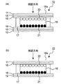
本発明に係る画像表示装置の代表的な構成断面を図2に示す。図2(a)は、基板11、12上に層構造の電極15を設け、電極15表面に絶縁層16を設けたものである。図2(b)に示す画像表示装置は、装置内に電極を設けていない構造のもので、装置外部に設けられた電極を介して電界を付与させ、表示粒子の移動を行える様にしたものである。図2(a)および図2(b)における同じ符号は同じ部材を意味するものとする。図2は図2(a)および図2(b)を包含して意味するものとする。図2の画像表示装置10は、図に示す様に、基板11側より画像を視認するものとするが、本発明では基板11側より画像を視認するものに限定されるものではない。また、図2(b)に示すタイプは、装置自体に電極15が設けられていない分、装置の構造を簡略化させ、その製造工程を短縮化することができるメリットがある。図2(b)に示すタイプの画像表示装置10を電圧印加可能な装置にセットして電圧印加を行う様子を示すものを図4に示す。なお、本発明に係る画像表示装置の断面構成は図2(a)と(b)に示すものに限定されるものではない。
FIG. 2 shows a typical cross section of the image display apparatus according to the present invention. FIG. 2A shows a structure in which an
図2(a)の画像表示装置10の最外部には、当該画像表示装置を構成する筐体である2つの基板11と12が対向して配置されている。基板11と12は双方が向き合う側の面上に電圧印加を行うための電極15が設けられ、さらに、電極15上に絶縁層16が設けられている。基板11と12には、電極15と絶縁層16が設けられ、電極15と絶縁層16を有する側の面を対向させて形成される隙間18には表示粒子が存在する。図2に示す画像表示装置10は、表示粒子として黒色表示粒子(以下、黒色粒子という)21と白色表示粒子(以下、白色粒子という)22の2種類の表示粒子を隙間18に存在させている。図2の画像表示装置10では、隙間18が基板11と12及び2つの隔壁17により四方を囲んだ構造となっており、表示粒子は隙間18に封入された状態で存在している。
At the outermost part of the
隙間18の厚さは、封入された表示粒子が移動可能で画像のコントラストを維持できる範囲であれば、特に限定されるものではなく、通常は10μm乃至500μm、好ましくは10μm乃至100μmである。隙間18内における表示粒子の体積占有率は、5%乃至70%であり、好ましくは30%乃至60%である。表示粒子の体積占有率を上記範囲にすることにより、隙間18内で表示粒子がスムーズに移動でき、また、コントラストのよい画像が得られる。
The thickness of the
次に、画像表示装置10の隙間18での表示粒子の挙動について説明する。
本発明に係る画像表示装置は、2枚の基板間に電圧を印加されて電界が形成されると、帯電している表示粒子は電界方向に沿って移動する様になる。この様に、表示粒子が存在する基板間に電圧を印加することにより、帯電した表示粒子が基板間を移動して画像表示を行うものである。
Next, the behavior of display particles in the
In the image display device according to the present invention, when a voltage is applied between two substrates to form an electric field, the charged display particles move along the electric field direction. In this way, when a voltage is applied between the substrates on which the display particles exist, the charged display particles move between the substrates to display an image.
本発明に係る画像表示装置における画像表示は以下の手順により行われるものである。
(1)表示媒体として用いる表示粒子を、キャリアによる摩擦帯電等の公知の方法により帯電させる。
(2)対向する2枚の基板間に表示粒子を封入し、この状態で基板間に電圧を印加する。
(3)基板間への電圧印加により、基板間に電界が形成される。
(4)表示粒子は、電極間の電界の力の作用により表示粒子の極性と反対側の電界方向に沿って基板表面に引き寄せられ、画像表示が行える様になる。
(5)また、基板間の電界方向を変えることにより、表示粒子の移動方向を切り換える。この移動方向の切換えにより画像表示を様々に変えることができる。
The image display in the image display apparatus according to the present invention is performed by the following procedure.
(1) The display particles used as the display medium are charged by a known method such as frictional charging with a carrier.
(2) Display particles are sealed between two opposing substrates, and a voltage is applied between the substrates in this state.
(3) An electric field is formed between the substrates by applying a voltage between the substrates.
(4) The display particles are attracted to the surface of the substrate along the direction of the electric field opposite to the polarity of the display particles by the action of the electric field force between the electrodes, so that image display can be performed.
(5) Further, the moving direction of the display particles is switched by changing the electric field direction between the substrates. The image display can be changed variously by switching the moving direction.
なお、上述した公知の方法による表示粒子の帯電方法としては、たとえば、キャリアに接触させて摩擦帯電により表示粒子を帯電させる方法、帯電極性の異なる2色の表示粒子を混合、撹拌して両者間の摩擦帯電により表示粒子を帯電させる方法等が挙げられるが、本発明では、キャリアを使用し、帯電した表示粒子を基板内に封入することが好ましい。 The display particles can be charged by the above-described known methods, for example, a method in which the display particles are charged by contact with a carrier by frictional charging, or two color display particles having different charging polarities are mixed and stirred. In the present invention, it is preferable to use a carrier and enclose the charged display particles in a substrate.
基板間への電圧印加に伴う表示粒子の移動の例を図3と図4に示す。
図3(a)は、基板11と12の間に電圧を印加する前の状態を示しており、電圧印加前は視認側の基板11近傍には正帯電した白色粒子22が存在している。この状態は画像表示装置10が白色画像を表示しているものである。また、図3(b)は、電極15に電圧を印加した後の状態を示しており、基板11に正の電圧を印加することで負に帯電した黒色粒子21が視認側の基板11近傍に移動し、白色粒子22は基板12側に移動している。この状態は画像表示装置10が黒色画像を表示しているものである。
An example of the movement of the display particles accompanying the voltage application between the substrates is shown in FIGS.
FIG. 3A shows a state before a voltage is applied between the
図4は、図2(b)に示した画像表示装置10に電極を有さないタイプのものを電圧印加装置30にセットし、この状態で電圧を印加する前の様子(図4(a))と電圧を印加した後の様子(図4(b))を示したものである。図2(b)に示すタイプの画像表示装置10も電極15を有する画像表示装置10と同様、基板11に正の電圧を印加することで負に帯電した黒色粒子21が視認側の基板11近傍に移動し、正に帯電した白色粒子22は基板12側に移動している。
FIG. 4 shows a state before the voltage is applied in this state in which the
次に、図2に示す画像表示装置10を構成する基板11、12、電極15、絶縁層16、および隔壁17について説明する。
Next, the
先ず、画像表示装置10を構成する基板11と12について説明する。画像表示装置10では、観察者は基板11と12の少なくとも一方の側から表示粒子により形成される画像を視認するので、観察者が視認する側に設けられる基板は透明な材質のものが求められる。したがって、観察者が画像を視認する側に使用される基板は、たとえば可視光透過率が80%以上の光透過性の材料が好ましく、80%以上の可視光透過率を有することにより十分な視認性が得られる。なお、画像表示装置10を構成する基板のうち、画像を視認する側の反対側に設けられる基板の材質は必ずしも透明なものである必要はない。
First, the
基板11、12の厚さは、それぞれ2μm〜5mmが好ましく、さらに、5μm〜2mmがより好ましい。基板11、12の厚さが上記範囲のとき、画像表示装置10に十分な強度を付与するとともに基板の間隔を均一に保つことができる。また、基板の厚さを上記範囲とすることでコンパクトで軽量な画像表示装置を提供することができるので、広い分野での当該画像表示装置の使用を促進させる。さらに、画像を視認する側の基板の厚みを上記範囲とすることにより、表示画像の正確な視認が行え表示品質に支障を与えない。
The thicknesses of the
可視光透過率が80%以上の材料としては、ガラスや石英等の可撓性を有さない無機材料や、後述する樹脂材料に代表される有機材料や金属シート等が挙げられる。このうち、有機材料や金属シートは画像表示装置にある程度の可撓性を付与することができる。可視光透過率を80%以上とすることが可能な樹脂材料としては、たとえば、ポリエチレンテレフタレートやポリエチレンナフタレート等に代表されるポリエステル樹脂や、ポリカーボネート樹脂、ポリエーテルスルホン樹脂、ポリイミド樹脂等が挙げられる。また、ポリメチルメタクリレート(PMMA)に代表されるアクリル酸エステルやメタクリル酸エステルの重合体であるアクリル樹脂やポリエチレン樹脂等のビニル系の重合性単量体をラジカル重合して得られる透明樹脂も挙げられる。 Examples of the material having a visible light transmittance of 80% or more include an inorganic material having no flexibility such as glass and quartz, an organic material typified by a resin material described later, a metal sheet, and the like. Among these, organic materials and metal sheets can impart a certain degree of flexibility to the image display device. Examples of the resin material having a visible light transmittance of 80% or more include polyester resins typified by polyethylene terephthalate and polyethylene naphthalate, polycarbonate resins, polyethersulfone resins, and polyimide resins. . In addition, a transparent resin obtained by radical polymerization of a vinyl polymerizable monomer such as an acrylic resin or a polyethylene resin, which is a polymer of acrylic acid ester or methacrylic acid ester represented by polymethyl methacrylate (PMMA). It is done.
電極15は基板11と12の面上に設けられ、電圧印加により基板間すなわち隙間18に電界を形成するものである。電極15は、前述の基板と同様に、観察者が画像を視認する側に透明なものを設ける必要がある。
The
画像を視認する側に設けられる電極の厚みは、導電性を確保するとともに光透過性に支障を来さないレベルにすることが求められ、具体的には3nm〜1μmが好ましく、5nm〜400nmがより好ましい。なお、画像を視認する側に設けられる電極の可視光透過率は、基板同様、80%以上とすることが好ましい。画像を視認する側の反対側に設けられる電極の厚みも上記範囲とすることが好ましいが、透明なものにする必要はない。 The thickness of the electrode provided on the side for visually recognizing the image is required to ensure conductivity and at a level that does not hinder the light transmittance. Specifically, the thickness is preferably 3 nm to 1 μm, and preferably 5 nm to 400 nm. More preferred. Note that the visible light transmittance of the electrode provided on the side where the image is viewed is preferably 80% or more, like the substrate. The thickness of the electrode provided on the side opposite to the side where the image is viewed is also preferably within the above range, but it is not necessary to be transparent.
電極15の構成材料としては、金属材料や導電性金属酸化物、あるいは、導電性高分子材料等が挙げられる。具体的な金属材料としては、たとえば、アルミニウム、銀、ニッケル、銅、金等が挙げられ、導電性金属酸化物の具体例としては、インジウム・スズ酸化物(ITO)、酸化インジウム、アンチモン・スズ酸化物(ATO)、酸化スズ、酸化亜鉛等が挙げられる。さらに、導電性高分子材料としては、たとえば、ポリアニリン、ポリピロール、ポリチオフェン、ポリアセチレン等が挙げられる。
Examples of the constituent material of the
電極15を基板11や12上に形成する方法としては、たとえば、薄膜上の電極を設ける場合には、スパッタリング法や真空蒸着法、化学蒸着法(CVD法;Chemical Vapor Deposition)、塗布法等が挙げられる。また、導電性材料を溶媒やバインダ樹脂に混合させ、この混合物を基板に塗布して電極を形成する方法もある。
As a method of forming the
絶縁層16は電極15の表面に設けられ、絶縁層16表面で表示粒子21,22と接触する構成となっているが、必ずしも設けなければならないというわけではない。絶縁層16は表示粒子21、22を移動させる際に印加される電圧によって帯電量の変化を緩和する役割をもっている。また、疎水性の高い構造をもつ樹脂、凹凸を付与することによって、表示粒子との物理的な付着力を低減でき、駆動電圧を低減させる働きももっている。絶縁層16を構成する材料としては、電気絶縁性を有する薄膜化可能な材料であって、所望により透明性を有するものである。画像を視認する側に設けられる絶縁層は可視光透過率を、基板同様、80%以上とすることが好ましい。具体例として、シリコーン樹脂、アクリル樹脂、ポリカーボネート樹脂等が挙げられる。
The insulating
絶縁層16の厚みは0.01μm以上10.0μm以下とすることが好ましい。すなわち、絶縁層16の厚みが上記範囲の時は、電極15間にそれほど大きな電圧を印加せずに表示粒子21,22が移動でき、たとえば、電気泳動法による画像形成で印加したレベルの電圧を付与して画像表示が行えるので好ましい。
The thickness of the insulating
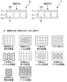
隔壁17は、上下基板間の隙間18を確保するものであり、図5上段の右側および左側の図に示すように基板11,12の縁部だけでなく、必要に応じて内部にも形成できる。隔壁17の幅、特に画像表示面18a側の隔壁の厚みは、例えば図5上段の右側の図に示すように、表示画像の鮮明性を確保する上からできるだけ薄くした方がよい。
The
基板11,12の内部に形成される隔壁17は、図5上段の右側および左側の図中、表裏方向に連続的に形成されても、断続的に形成されてもよい。
隔壁17の形状および配置を制御することにより、隔壁17により仕切られた隙間18のセルを様々な形状で配置できる。隙間18を基板11の視認方向から見た時のセルの形状および配置の例を図5下段の図に示す。セルは、図5下段の図に示すように、四角形状、三角形状、ライン状、円形状、六角形状等にて、複数個で、ハニカム状や網目状に配置することができる。
The
By controlling the shape and arrangement of the
隔壁17は、たとえば以下に挙げる方法を用いて画像を視認する側の反対側の基板上を加工処理することにより形成できる。隔壁17を形成する方法としては、たとえば、樹脂材料等によるエンボス加工や熱プレス射出成形による凹凸形成、フォトリソグラフ法やスクリーン印刷等が挙げられる。
The
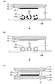
画像表示装置は、例えば以下に示す電子写真現像方式によって製造可能である。
2枚の基板11に、電極15および所望により絶縁層16を形成し、一対の電極付き基板を得る。表示粒子21およびキャリア210を混合することにより表示粒子21を負帯電させ、混合物(21,210)を、図6(a)に示すように、導電性のステージ100上に置き、一方の電極付き基板を、ステージ100と所定の間隔を空けて設置する。次いで、図6(a)に示すように、電極15に正極性の直流電圧と交流電圧を印加して、負帯電性表示粒子21を付着させる。
表示粒子22およびキャリア220を混合することにより表示粒子22を正帯電させ、混合物(22,220)を、図6(b)に示すように、導電性のステージ100上に置き、他方の電極付き基板を、ステージ100と所定の間隔を空けて設置する。次いで、図6(b)に示すように、電極15に負極性の直流電圧と交流電圧を印加して、正帯電性表示粒子22を付着させる。負帯電性表示粒子を付着させた電極付き基板と、正帯電性表示粒子を付着させた電極付き基板とを、図6(c)に示すように、所定の間隔になるように隔壁で調整して重ね、基板周辺を接着し、画像表示装置を得ることができる。
The image display device can be manufactured by, for example, the following electrophotographic development method.
The
By mixing the
表示粒子を負帯電させるキャリア210としては、フェライト等の磁性粒子に、シクロヘキシルメタクリレート樹脂等の樹脂をコートしたコート型キャリアが有用である。
表示粒子を正帯電させるキャリア220としては、フェライト等の磁性粒子に、フッ素化アクリレート樹脂等の樹脂をコートしたコート型キャリアが有用である。
As the
As the
<実施例1>
[黒色表示粒子の製造]
(黒色母体粒子)
下記した樹脂及びカーボンブラックをヘンシェルミキサ(三井三池鉱業社製)に投入し、撹拌羽根の周速を25m/秒に設定して5分間混合処理して混合物とした。
スチレンアクリル樹脂(重量平均分子量20,000) 100重量部
カーボンブラック(平均一次粒径25nm) 10重量部
上記混合物を二軸押出混練機で混練し、次いで、ハンマーミルで粗粉砕した後、ターボミル粉砕機(ターボ工業社製)で粗粉粉砕し、さらに、コアンダ効果を利用した気流分級機で微粉分級処理を行って、体積平均粒径が8.2μmの黒色母体粒子を製造した。
<Example 1>
[Production of black display particles]
(Black matrix particles)
The resin and carbon black described below were put into a Henschel mixer (manufactured by Mitsui Miike Mining Co., Ltd.), the peripheral speed of the stirring blade was set to 25 m / sec, and the mixture was mixed for 5 minutes to obtain a mixture.
Styrene acrylic resin (weight average molecular weight 20,000) 100 parts by weight Carbon black (average primary particle size 25 nm) 10 parts by weight The above mixture is kneaded with a twin-screw extrusion kneader, then coarsely pulverized with a hammer mill, and then turbo milled. Coarse powder was pulverized by a machine (manufactured by Turbo Kogyo Co., Ltd.), and further finely classified by an airflow classifier utilizing the Coanda effect to produce black matrix particles having a volume average particle size of 8.2 μm.
(金属酸化物層)
黒色母体粒子30gを純水1000gに分散し、アンモニア水(28wt%)10gを添加して5分間攪拌した。次いでテトラエトキシシラン8.5gとジメチルジエトキシシラン8.5gを3時間かけて滴下し、さらに室温にて5時間攪拌した。得られた沈殿物をろ過し、純水にて洗浄した後、60℃で24時間乾燥し、白色母体粒子表面にシリカ微粒子層が形成された黒色表示粒子を得た。
(Metal oxide layer)
30 g of black base particles were dispersed in 1000 g of pure water, 10 g of ammonia water (28 wt%) was added and stirred for 5 minutes. Next, 8.5 g of tetraethoxysilane and 8.5 g of dimethyldiethoxysilane were added dropwise over 3 hours, and the mixture was further stirred at room temperature for 5 hours. The obtained precipitate was filtered, washed with pure water, and then dried at 60 ° C. for 24 hours to obtain black display particles having a silica fine particle layer formed on the surface of white base particles.
(黒色表示粒子の有機層)
金属酸化物層を形成された黒色表示粒子10gを室温で、シクロヘキサン50gとヘキサメチルジシラザン10gとの混合液に加えて、この分散液を撹拌しながら50℃に加熱し、3時間反応させた。次いで、この分散液中の溶媒を50℃、減圧下で留去することにより、黒色表示粒子を得た。
(Organic layer of black display particles)
10 g of black display particles on which a metal oxide layer has been formed are added to a mixed liquid of 50 g of cyclohexane and 10 g of hexamethyldisilazane at room temperature, and this dispersion is heated to 50 ° C. with stirring to react for 3 hours. . Subsequently, the solvent in this dispersion was distilled off at 50 ° C. under reduced pressure to obtain black display particles.
[白色表示粒子の製造]
(白色母体粒子)
下記した樹脂及び酸化チタンをヘンシェルミキサ(三井三池鉱業社製)に投入し、撹拌羽根の周速を25m/秒に設定して5分間混合処理して混合物とした。
スチレンアクリル樹脂(重量平均分子量20,000) 100重量部
ルチル型酸化チタン(R−630;石原産業社製) 100重量部
上記混合物を二軸押出混練機で混練し、次いで、ハンマーミルで粗粉砕した後、ターボミル粉砕機(ターボ工業社製)で粉砕処理し、さらに、コアンダ効果を利用した気流分級機で微粉分級処理を行って、体積平均粒径が8.0μmの白色母体粒子を製造した。
[Manufacture of white display particles]
(White matrix particles)
The resin and titanium oxide described below were put into a Henschel mixer (manufactured by Mitsui Miike Mining Co., Ltd.), the peripheral speed of the stirring blade was set to 25 m / second, and the mixture was mixed for 5 minutes to obtain a mixture.
Styrene acrylic resin (weight average molecular weight 20,000) 100 parts by weight Rutile type titanium oxide (R-630; manufactured by Ishihara Sangyo Co., Ltd.) 100 parts by weight The above mixture is kneaded with a twin-screw extrusion kneader and then coarsely pulverized with a hammer mill After that, it was pulverized by a turbo mill pulverizer (manufactured by Turbo Kogyo Co., Ltd.), and further finely classified by an airflow classifier utilizing the Coanda effect to produce white base particles having a volume average particle size of 8.0 μm. .
(金属酸化物層)
白色母体粒子30gを純水1000gに分散し、アンモニア水(28wt%)10gを添加して5分間攪拌した。次いでテトラエトキシシラン8.5gとジメチルジエトキシシラン8.5gを3時間かけて滴下し、さらに室温にて5時間攪拌した。得られた沈殿物をろ過し、純水にて洗浄した後、60℃で24時間乾燥し、白色母体粒子表面にシリカ微粒子層が形成された白色表示粒子を得た。
(Metal oxide layer)
30 g of white base particles were dispersed in 1000 g of pure water, 10 g of ammonia water (28 wt%) was added, and the mixture was stirred for 5 minutes. Next, 8.5 g of tetraethoxysilane and 8.5 g of dimethyldiethoxysilane were added dropwise over 3 hours, and the mixture was further stirred at room temperature for 5 hours. The obtained precipitate was filtered, washed with pure water, and then dried at 60 ° C. for 24 hours to obtain white display particles in which a silica fine particle layer was formed on the surface of the white base particles.
(白色表示粒子の有機層)
酢酸水溶液(1wt%)25gにN−(2−アミノエチル)−3−アミノプロピルトリエトキシシラン(第1処理剤)4gを加えて、室温で15分間攪拌した。その後、混合液に、金属酸化物層を形成された白色表示粒子10gを添加し、50℃で3時間攪拌した。この分散液中の溶媒を50℃、減圧下で留去した。その後、さらに、得られた白色粒子をシクロヘキサン50gとヘキサメチルジシラザン(第2処理剤)10gとの混合液に加えて、撹拌しながら50℃に加熱し、3時間反応させた。次いで、この分散液中の溶媒を50℃、減圧下で留去することにより、白色表示粒子を得た。
(Organic layer of white display particles)
4 g of N- (2-aminoethyl) -3-aminopropyltriethoxysilane (first treatment agent) was added to 25 g of an acetic acid aqueous solution (1 wt%), and the mixture was stirred at room temperature for 15 minutes. Thereafter, 10 g of white display particles having a metal oxide layer formed thereon were added to the mixed solution, and the mixture was stirred at 50 ° C. for 3 hours. The solvent in this dispersion was distilled off at 50 ° C. under reduced pressure. Thereafter, the obtained white particles were further added to a mixed liquid of 50 g of cyclohexane and 10 g of hexamethyldisilazane (second treatment agent), heated to 50 ° C. with stirring, and reacted for 3 hours. Subsequently, the solvent in this dispersion was distilled off at 50 ° C. under reduced pressure to obtain white display particles.
[白色表示粒子を帯電させるためのキャリアA]
平均粒子径80μmのフェライトコア100重量部に対して、フッ素化アクリレート樹脂粒子を2部加え、これら原料を水平回転翼型混合機に投入し、水平回転翼の周速が8m/秒となる条件で22℃で10分間混合攪拌した後、90℃に加熱し40分攪拌して、キャリアAを製造した。
[Carrier A for charging white display particles]
Conditions in which 2 parts of fluorinated acrylate resin particles are added to 100 parts by weight of ferrite core having an average particle diameter of 80 μm, and these raw materials are put into a horizontal rotary blade type mixer so that the peripheral speed of the horizontal rotary blade is 8 m / sec. Was mixed and stirred at 22 ° C. for 10 minutes, and then heated to 90 ° C. and stirred for 40 minutes to produce Carrier A.
[黒色表示粒子を帯電させるためのキャリアB]
平均粒子径80μmのフェライトコア100重量部に対して、シクロヘキシルメタクリレート樹脂粒子を2部加え、これら原料を水平回転翼型混合機に投入し、水平回転翼の周速が8m/秒となる条件で22℃で10分間混合攪拌した後、90℃に加熱し40分攪拌して、キャリアBを製造した。
[Carrier B for charging black display particles]
Under the condition that 2 parts of cyclohexyl methacrylate resin particles are added to 100 parts by weight of a ferrite core having an average particle diameter of 80 μm, and these raw materials are put into a horizontal rotary blade type mixer so that the peripheral speed of the horizontal rotary blade is 8 m / sec. After mixing and stirring at 22 ° C. for 10 minutes, carrier B was produced by heating to 90 ° C. and stirring for 40 minutes.
[画像表示装置の製造]
画像表示装置は、図2(a)と同様の構造を有するように、以下の方法に従って製造した。長さ80mm、幅50mm、厚さ0.7mmのガラス基板11を2枚用意し、各基板面上には、厚さ300nmのインジウム・スズ酸化物(ITO)被膜(抵抗30Ω/□)からなる電極15を蒸着法により形成した。上記電極上に、ポリカーボネート樹脂12gを、テトラヒドロフラン80mlとシクロヘキサノン20mlの混合溶媒に溶解させてなる塗布液を、スピンコート法により塗布して厚さ3μmの絶縁層16を形成し、一対の電極付き基板を得た。
[Manufacture of image display devices]
The image display device was manufactured according to the following method so as to have the same structure as that shown in FIG. Two
黒色表示粒子1gおよびキャリアB 9gを振とう機(YS−LD ヤヨイ社製)により30分間混合することにより、表示粒子を帯電させた。得られた混合物(21,210)を、図6(a)に示すように、導電性のステージ100上に置き、一方の電極付き基板を、ステージ100と約2mmの間隔を空けて設置した。電極15とステージ100との間に、DCバイアス+50V,ACバイアス2.0kV,周波数2.0kHzを10秒間印加して、絶縁層16上に黒色表示粒子21を付着させた。
The display particles were charged by mixing 30 g of black display particles 1 g and carrier B 9 g with a shaker (manufactured by YS-LD Yayoi Co., Ltd.) for 30 minutes. As shown in FIG. 6A, the obtained mixture (21, 210) was placed on a
白色表示粒子1gおよびキャリアA 9gを振とう機(YS−LD ヤヨイ社製)により30分間混合することにより、表示粒子を帯電させた。得られた混合物(22,220)を、図6(b)に示すように、導電性のステージ100上に置き、他方の電極付き基板を、ステージ100と約2mmの間隔を空けて設置した。電極15とステージ100との間に、DCバイアス−50V,ACバイアス2.0kV,周波数2.0kHzを10秒間印加して、絶縁層16上に白色表示粒子22を付着させた。
The display particles were charged by mixing 1 g of white display particles and 9 g of carrier A for 30 minutes with a shaker (manufactured by YS-LD Yayoi Co., Ltd.). As shown in FIG. 6B, the obtained mixture (22, 220) was placed on a
黒色表示粒子を付着させた電極付き基板と、白色表示粒子を付着させた電極付き基板とを、図6(c)に示すように、間隔50μmになるように隔壁で調整して重ね、基板周辺をエポキシ系接着剤にて接着し、画像表示装置とした。なお、2種類の表示粒子のガラス基板間への体積占有率は50%であった。白色表示粒子と黒色表示粒子との含有割合は白色表示粒子/黒色表示粒子の重量比で1/1にしてある。 As shown in FIG. 6C, the substrate with electrodes to which black display particles are attached and the substrate with electrodes to which white display particles are attached are adjusted and overlapped with a partition so as to have an interval of 50 μm. Were bonded with an epoxy adhesive to obtain an image display device. The volume occupation ratio between the two types of display particles between the glass substrates was 50%. The content ratio of the white display particles and the black display particles is set to 1/1 by the weight ratio of the white display particles / black display particles.
<実施例2〜7/比較例1〜2>
白色表示粒子および黒色表示粒子の製造時において、表1および表2に示す所定の化合物Aおよび化合物Bを所定の比率で用いたこと以外、実施例1と同様の方法により、画像表示装置を製造した。
<Examples 2-7 / Comparative Examples 1-2>
An image display device is manufactured in the same manner as in Example 1 except that the predetermined compound A and compound B shown in Table 1 and Table 2 are used at a predetermined ratio when white display particles and black display particles are manufactured. did.

<評価>
画像表示装置に対して以下の手順で直流電圧を印加し、電圧印加により得られる表示画像の反射濃度を測定することにより、表示特性を評価した。尚、電圧印加は、以下の手順で行い、印加電圧を0Vからプラス側に変化させた後、続いてマイナス側に変化させ、再び0Vに戻る経路のヒステリシス曲線を描く様に電圧を印加した。すなわち、
(1)0Vから+100Vまで20V間隔で電圧を変化させながら印加を行う。
(2)+100Vから−100Vまで20V間隔で電圧を変化させながら印加を行う。
(3)−100Vより0Vまで20V間隔で電圧を変化させながら印加を行う。
上記手順で各画像表示装置に直流電圧を印加したところ、白表示の状態でプラスの電圧を印加した時に、表示が白から黒に変化することが確認された。なお、画像表示装置の視認方向上流側の電極に印加する電圧を変化させ、他方の電極は電気的に接地させた。
<Evaluation>
The display characteristics were evaluated by applying a DC voltage to the image display device according to the following procedure and measuring the reflection density of the display image obtained by the voltage application. The voltage application was performed according to the following procedure. The applied voltage was changed from 0V to the plus side, then changed to the minus side, and the voltage was applied so as to draw a hysteresis curve of a path returning to 0V again. That is,
(1) Application is performed while changing the voltage from 0V to + 100V at intervals of 20V.
(2) Application is performed while changing the voltage from + 100V to −100V at intervals of 20V.
(3) Application is performed while changing the voltage from −100V to 0V at intervals of 20V.
When a DC voltage was applied to each image display device according to the above procedure, it was confirmed that the display changed from white to black when a positive voltage was applied in a white display state. The voltage applied to the electrode on the upstream side in the visual recognition direction of the image display device was changed, and the other electrode was electrically grounded.
コントラストは、黒色濃度と白色濃度との差、すなわち、
コントラスト=黒色濃度−白色濃度
で定義される濃度差により評価した。
黒色濃度は、画像表示装置の視認方向上流側の電極に+100Vの電圧を印加した時に得られる表示面の反射濃度である。
白色濃度は、画像表示装置の視認方向上流側の電極に−100Vの電圧を印加した時に得られる表示面の反射濃度である。
濃度は、反射濃度計「RD−918(マクベス社製)」を用いて、表示面上の5カ所をランダムに測定して、その平均値とした。
Contrast is the difference between black density and white density, i.e.
Evaluation was based on a density difference defined by contrast = black density−white density.
The black density is the reflection density of the display surface obtained when a voltage of +100 V is applied to the electrode on the upstream side in the viewing direction of the image display device.
The white density is a reflection density of the display surface obtained when a voltage of −100 V is applied to the electrode on the upstream side in the viewing direction of the image display device.
The density was averaged by measuring five locations on the display surface at random using a reflection densitometer “RD-918 (manufactured by Macbeth)”.
(コントラスト耐久性)
繰り返し特性は、+100Vと−100Vの電圧印加を交互に繰り返し、その都度反射濃度を測定したとき、コントラストが0.70以下になった時点での繰り返し回数に基づいて評価した。繰り返し回数が50000回以上を優良(○)、30000回以上を合格(△)、30000回未満を不合格(×)とした。
(Contrast durability)
The repetition characteristics were evaluated based on the number of repetitions when the contrast became 0.70 or less when the voltage application of +100 V and −100 V were alternately repeated and the reflection density was measured each time. The number of repetitions was 50000 times or more as excellent (◯), 30000 times or more as acceptable (Δ), and less than 30000 times as unacceptable (x).
1:樹脂、2:着色剤、3:母体粒子、4:金属酸化物層、5:有機層、10:画像表示装置、11:12:基板、15:電極、16:絶縁層、17:隔壁、18:隙間、18a:画像表示面、21:黒色表示粒子、22:白色表示粒子。 1: Resin, 2: Colorant, 3: Base particles, 4: Metal oxide layer, 5: Organic layer, 10: Image display device, 11:12: Substrate, 15: Electrode, 16: Insulating layer, 17: Partition wall , 18: gap, 18a: image display surface, 21: black display particles, 22: white display particles.
Claims (5)
表示粒子が、少なくとも樹脂および着色剤を含有する母体粒子の表面に金属酸化物層を有し、
金属酸化物層が一般式(A);
M1(OR1)4 (A)
(式中、M1はケイ素原子またはチタン原子を示す;R1はそれぞれ独立して炭素数1〜4のアルキル基を示す)で表される化合物Aおよび一般式(B);
M2(R2)4−n(OR3)n (B)
(式中、M2はケイ素原子またはチタン原子を示す;R2はそれぞれ独立して炭素数1〜4のアルキル基、フェニル基、アクリロイルオキシ基、メタクリロイルオキシ基またはエポキシ基を示す;R3はそれぞれ独立して炭素数1〜4のアルキル基を示す;nは2または3を示す)で表される化合物Bを含む重縮合物からなる画像表示装置用表示粒子。 A display used in an image display device that displays an image by moving display particles by encapsulating display particles in a powder form between two substrates transparent at least one and generating an electric field between the substrates. Particles,
The display particles have a metal oxide layer on the surface of the base particles containing at least a resin and a colorant,
The metal oxide layer has the general formula (A);
M 1 (OR 1 ) 4 (A)
(Wherein, M 1 represents a silicon atom or a titanium atom; R 1 independently represents an alkyl group having 1 to 4 carbon atoms) and the general formula (B);
M 2 (R 2 ) 4-n (OR 3 ) n (B)
(Wherein M 2 represents a silicon atom or a titanium atom; R 2 independently represents an alkyl group having 1 to 4 carbon atoms, a phenyl group, an acryloyloxy group, a methacryloyloxy group or an epoxy group; R 3 represents Display particles for an image display device comprising a polycondensate containing Compound B, each independently representing an alkyl group having 1 to 4 carbon atoms; n represents 2 or 3.
Priority Applications (2)
| Application Number | Priority Date | Filing Date | Title |
|---|---|---|---|
| JP2009145421A JP2011002644A (en) | 2009-06-18 | 2009-06-18 | Display particle for image display and image display |
| US12/814,556 US8248685B2 (en) | 2009-06-18 | 2010-06-14 | Display particles for image display apparatus and image display apparatus loaded with the same |
Applications Claiming Priority (1)
| Application Number | Priority Date | Filing Date | Title |
|---|---|---|---|
| JP2009145421A JP2011002644A (en) | 2009-06-18 | 2009-06-18 | Display particle for image display and image display |
Publications (2)
| Publication Number | Publication Date |
|---|---|
| JP2011002644A true JP2011002644A (en) | 2011-01-06 |
| JP2011002644A5 JP2011002644A5 (en) | 2012-03-29 |
Family
ID=43354111
Family Applications (1)
| Application Number | Title | Priority Date | Filing Date |
|---|---|---|---|
| JP2009145421A Pending JP2011002644A (en) | 2009-06-18 | 2009-06-18 | Display particle for image display and image display |
Country Status (2)
| Country | Link |
|---|---|
| US (1) | US8248685B2 (en) |
| JP (1) | JP2011002644A (en) |
Cited By (1)
| Publication number | Priority date | Publication date | Assignee | Title |
|---|---|---|---|---|
| JP2015537238A (en) * | 2012-10-10 | 2015-12-24 | キュースペックス テクノロジーズ インコーポレイテッドQspex Technologies,Inc. | Antireflection lens and manufacturing method thereof |
Families Citing this family (5)
| Publication number | Priority date | Publication date | Assignee | Title |
|---|---|---|---|---|
| JP5099217B2 (en) * | 2008-09-12 | 2012-12-19 | コニカミノルタビジネステクノロジーズ株式会社 | Display particles for image display device and image display device |
| US8557877B2 (en) * | 2009-06-10 | 2013-10-15 | Honeywell International Inc. | Anti-reflective coatings for optically transparent substrates |
| US9335443B2 (en) | 2011-04-15 | 2016-05-10 | Qspex Technologies, Inc. | Anti-reflective lenses and methods for manufacturing the same |
| US8864898B2 (en) | 2011-05-31 | 2014-10-21 | Honeywell International Inc. | Coating formulations for optical elements |
| JP5942394B2 (en) * | 2011-11-22 | 2016-06-29 | ソニー株式会社 | Electrophoretic element and display device |
Citations (8)
| Publication number | Priority date | Publication date | Assignee | Title |
|---|---|---|---|---|
| JPS4856230A (en) * | 1971-11-19 | 1973-08-07 | ||
| JPS62275170A (en) * | 1986-05-23 | 1987-11-30 | Matsushita Electric Works Ltd | Production of coating material |
| JPH08185619A (en) * | 1994-12-28 | 1996-07-16 | Fuji Photo Film Co Ltd | Magnetic recording medium and its production |
| JP2006023158A (en) * | 2004-07-07 | 2006-01-26 | Denso Corp | Navigation system for car |
| JP2006106596A (en) * | 2004-10-08 | 2006-04-20 | Bridgestone Corp | Particle for display medium used for panel for information display |
| JP2006162723A (en) * | 2004-12-03 | 2006-06-22 | Chisso Corp | Silicon-contained particulate and electrophoretic type display element containing same |
| JP2007169507A (en) * | 2005-12-22 | 2007-07-05 | Chisso Corp | Ammonium silane-modified silicon-containing particle, display liquid for electrophoretic display device and electrophoretic display element containing the same |
| WO2008029620A1 (en) * | 2006-09-08 | 2008-03-13 | Central Glass Company, Limited | Heat ray shielding glass for vehicle and process for producing the same |
Family Cites Families (5)
| Publication number | Priority date | Publication date | Assignee | Title |
|---|---|---|---|---|
| JP4456803B2 (en) | 2001-09-19 | 2010-04-28 | 株式会社ブリヂストン | Image display particle and image display device |
| JP2004029699A (en) | 2002-05-02 | 2004-01-29 | Bridgestone Corp | Particles for picture display, and picture display device using the same |
| JP4945099B2 (en) | 2004-08-05 | 2012-06-06 | 株式会社ブリヂストン | Particles for display medium and information display panel using the same |
| JP2009251084A (en) * | 2008-04-02 | 2009-10-29 | Konica Minolta Business Technologies Inc | Image display device |
| JP5262797B2 (en) * | 2009-02-16 | 2013-08-14 | コニカミノルタビジネステクノロジーズ株式会社 | Image display device |
-
2009
- 2009-06-18 JP JP2009145421A patent/JP2011002644A/en active Pending
-
2010
- 2010-06-14 US US12/814,556 patent/US8248685B2/en not_active Expired - Fee Related
Patent Citations (8)
| Publication number | Priority date | Publication date | Assignee | Title |
|---|---|---|---|---|
| JPS4856230A (en) * | 1971-11-19 | 1973-08-07 | ||
| JPS62275170A (en) * | 1986-05-23 | 1987-11-30 | Matsushita Electric Works Ltd | Production of coating material |
| JPH08185619A (en) * | 1994-12-28 | 1996-07-16 | Fuji Photo Film Co Ltd | Magnetic recording medium and its production |
| JP2006023158A (en) * | 2004-07-07 | 2006-01-26 | Denso Corp | Navigation system for car |
| JP2006106596A (en) * | 2004-10-08 | 2006-04-20 | Bridgestone Corp | Particle for display medium used for panel for information display |
| JP2006162723A (en) * | 2004-12-03 | 2006-06-22 | Chisso Corp | Silicon-contained particulate and electrophoretic type display element containing same |
| JP2007169507A (en) * | 2005-12-22 | 2007-07-05 | Chisso Corp | Ammonium silane-modified silicon-containing particle, display liquid for electrophoretic display device and electrophoretic display element containing the same |
| WO2008029620A1 (en) * | 2006-09-08 | 2008-03-13 | Central Glass Company, Limited | Heat ray shielding glass for vehicle and process for producing the same |
Cited By (1)
| Publication number | Priority date | Publication date | Assignee | Title |
|---|---|---|---|---|
| JP2015537238A (en) * | 2012-10-10 | 2015-12-24 | キュースペックス テクノロジーズ インコーポレイテッドQspex Technologies,Inc. | Antireflection lens and manufacturing method thereof |
Also Published As
| Publication number | Publication date |
|---|---|
| US20100321762A1 (en) | 2010-12-23 |
| US8248685B2 (en) | 2012-08-21 |
Similar Documents
| Publication | Publication Date | Title |
|---|---|---|
| JP2009244551A (en) | Display particle for image display apparatus, and image display apparatus | |
| JP4579822B2 (en) | Image display panel and image display device | |
| JP2011002644A (en) | Display particle for image display and image display | |
| JP2002072256A (en) | Image display medium | |
| JP2009086135A (en) | Image display apparatus | |
| JP2009251084A (en) | Image display device | |
| JP5396875B2 (en) | Display particles for image display device and image display device | |
| JP2010190962A (en) | Display particle for image display device, and image display device | |
| JP5262797B2 (en) | Image display device | |
| JP5099217B2 (en) | Display particles for image display device and image display device | |
| JP4945099B2 (en) | Particles for display medium and information display panel using the same | |
| JP2010276782A (en) | Image display apparatus | |
| JP2010282012A (en) | Display particle for image display device, and the image display device | |
| JP5228638B2 (en) | Display particles for image display device and image display device | |
| JP5131042B2 (en) | Image display device | |
| JP5381036B2 (en) | White display particles and image display device | |
| JP5298920B2 (en) | Display particles for image display device and image display device | |
| JP5315962B2 (en) | Display particles for image display device and image display device | |
| JP2013024924A (en) | Image display method and image display element used therefor | |
| JP2010026451A (en) | Display particle for image display and image display | |
| JP2011007844A (en) | Display particle for image display and image display | |
| JP2010061061A (en) | Display particles for image display device and image display device | |
| JP2010128075A (en) | Display particle for image display device and image display device | |
| JP2009216879A (en) | Display particle for image display device and image display device | |
| JP2010122256A (en) | White display particle and image display |
Legal Events
| Date | Code | Title | Description |
|---|---|---|---|
| A621 | Written request for application examination |
Free format text: JAPANESE INTERMEDIATE CODE: A621 Effective date: 20120120 |
|
| A521 | Request for written amendment filed |
Free format text: JAPANESE INTERMEDIATE CODE: A523 Effective date: 20120210 |
|
| A977 | Report on retrieval |
Free format text: JAPANESE INTERMEDIATE CODE: A971007 Effective date: 20130312 |
|
| A711 | Notification of change in applicant |
Free format text: JAPANESE INTERMEDIATE CODE: A712 Effective date: 20130415 |
|
| A02 | Decision of refusal |
Free format text: JAPANESE INTERMEDIATE CODE: A02 Effective date: 20140311 |