JP2010532016A - Liquid crystal display panel and manufacturing method thereof - Google Patents
Liquid crystal display panel and manufacturing method thereof Download PDFInfo
- Publication number
- JP2010532016A JP2010532016A JP2010514918A JP2010514918A JP2010532016A JP 2010532016 A JP2010532016 A JP 2010532016A JP 2010514918 A JP2010514918 A JP 2010514918A JP 2010514918 A JP2010514918 A JP 2010514918A JP 2010532016 A JP2010532016 A JP 2010532016A
- Authority
- JP
- Japan
- Prior art keywords
- liquid crystal
- trace
- parallel conductive
- substrate
- layer
- Prior art date
- Legal status (The legal status is an assumption and is not a legal conclusion. Google has not performed a legal analysis and makes no representation as to the accuracy of the status listed.)
- Withdrawn
Links
- 239000004973 liquid crystal related substance Substances 0.000 title claims abstract description 148
- 238000004519 manufacturing process Methods 0.000 title claims description 13
- 239000000758 substrate Substances 0.000 claims abstract description 109
- 239000000463 material Substances 0.000 claims abstract description 65
- 210000002858 crystal cell Anatomy 0.000 claims abstract description 56
- 229920000307 polymer substrate Polymers 0.000 claims abstract description 47
- 238000000034 method Methods 0.000 claims description 43
- 239000004986 Cholesteric liquid crystals (ChLC) Substances 0.000 claims description 21
- 210000004027 cell Anatomy 0.000 claims description 16
- 238000005520 cutting process Methods 0.000 claims description 9
- 238000000926 separation method Methods 0.000 claims 1
- 239000011159 matrix material Substances 0.000 description 13
- 239000011248 coating agent Substances 0.000 description 12
- 238000000576 coating method Methods 0.000 description 12
- 150000001875 compounds Chemical class 0.000 description 12
- 229920000642 polymer Polymers 0.000 description 9
- -1 polyethylene Polymers 0.000 description 6
- 238000003475 lamination Methods 0.000 description 5
- 229920000106 Liquid crystal polymer Polymers 0.000 description 4
- 239000004988 Nematic liquid crystal Substances 0.000 description 4
- 239000004983 Polymer Dispersed Liquid Crystal Substances 0.000 description 4
- 238000003698 laser cutting Methods 0.000 description 4
- 238000006116 polymerization reaction Methods 0.000 description 4
- KFZMGEQAYNKOFK-UHFFFAOYSA-N Isopropanol Chemical compound CC(C)O KFZMGEQAYNKOFK-UHFFFAOYSA-N 0.000 description 3
- OKKJLVBELUTLKV-UHFFFAOYSA-N Methanol Chemical compound OC OKKJLVBELUTLKV-UHFFFAOYSA-N 0.000 description 3
- 239000004020 conductor Substances 0.000 description 3
- 238000001723 curing Methods 0.000 description 3
- 239000003999 initiator Substances 0.000 description 3
- 230000003287 optical effect Effects 0.000 description 3
- 238000005191 phase separation Methods 0.000 description 3
- 239000004417 polycarbonate Substances 0.000 description 3
- 229920000515 polycarbonate Polymers 0.000 description 3
- 238000004080 punching Methods 0.000 description 3
- 239000002904 solvent Substances 0.000 description 3
- 239000004977 Liquid-crystal polymers (LCPs) Substances 0.000 description 2
- UFWIBTONFRDIAS-UHFFFAOYSA-N Naphthalene Chemical compound C1=CC=CC2=CC=CC=C21 UFWIBTONFRDIAS-UHFFFAOYSA-N 0.000 description 2
- XYFCBTPGUUZFHI-UHFFFAOYSA-N Phosphine Chemical compound P XYFCBTPGUUZFHI-UHFFFAOYSA-N 0.000 description 2
- 239000004642 Polyimide Substances 0.000 description 2
- XLOMVQKBTHCTTD-UHFFFAOYSA-N Zinc monoxide Chemical compound [Zn]=O XLOMVQKBTHCTTD-UHFFFAOYSA-N 0.000 description 2
- 239000012965 benzophenone Substances 0.000 description 2
- IISBACLAFKSPIT-UHFFFAOYSA-N bisphenol A Chemical compound C=1C=C(O)C=CC=1C(C)(C)C1=CC=C(O)C=C1 IISBACLAFKSPIT-UHFFFAOYSA-N 0.000 description 2
- 230000003098 cholesteric effect Effects 0.000 description 2
- 238000010586 diagram Methods 0.000 description 2
- 238000004049 embossing Methods 0.000 description 2
- 238000005516 engineering process Methods 0.000 description 2
- AMGQUBHHOARCQH-UHFFFAOYSA-N indium;oxotin Chemical compound [In].[Sn]=O AMGQUBHHOARCQH-UHFFFAOYSA-N 0.000 description 2
- 238000002156 mixing Methods 0.000 description 2
- 229920000728 polyester Polymers 0.000 description 2
- 229920000139 polyethylene terephthalate Polymers 0.000 description 2
- 239000005020 polyethylene terephthalate Substances 0.000 description 2
- 229920001721 polyimide Polymers 0.000 description 2
- 239000002861 polymer material Substances 0.000 description 2
- 239000000126 substance Substances 0.000 description 2
- 229920001169 thermoplastic Polymers 0.000 description 2
- JNELGWHKGNBSMD-UHFFFAOYSA-N xanthone Chemical compound C1=CC=C2C(=O)C3=CC=CC=C3OC2=C1 JNELGWHKGNBSMD-UHFFFAOYSA-N 0.000 description 2
- NLGDWWCZQDIASO-UHFFFAOYSA-N 2-hydroxy-1-(7-oxabicyclo[4.1.0]hepta-1,3,5-trien-2-yl)-2-phenylethanone Chemical compound OC(C(=O)c1cccc2Oc12)c1ccccc1 NLGDWWCZQDIASO-UHFFFAOYSA-N 0.000 description 1
- LFQSCWFLJHTTHZ-UHFFFAOYSA-N Ethanol Chemical compound CCO LFQSCWFLJHTTHZ-UHFFFAOYSA-N 0.000 description 1
- 206010073306 Exposure to radiation Diseases 0.000 description 1
- 239000004952 Polyamide Substances 0.000 description 1
- 239000004698 Polyethylene Substances 0.000 description 1
- 239000004743 Polypropylene Substances 0.000 description 1
- 239000004793 Polystyrene Substances 0.000 description 1
- 238000010521 absorption reaction Methods 0.000 description 1
- 239000011324 bead Substances 0.000 description 1
- RWCCWEUUXYIKHB-UHFFFAOYSA-N benzophenone Chemical compound C=1C=CC=CC=1C(=O)C1=CC=CC=C1 RWCCWEUUXYIKHB-UHFFFAOYSA-N 0.000 description 1
- 230000015572 biosynthetic process Effects 0.000 description 1
- 238000005229 chemical vapour deposition Methods 0.000 description 1
- 238000007334 copolymerization reaction Methods 0.000 description 1
- 239000012769 display material Substances 0.000 description 1
- 230000005684 electric field Effects 0.000 description 1
- 238000011049 filling Methods 0.000 description 1
- 229930192419 itoside Natural products 0.000 description 1
- 239000000178 monomer Substances 0.000 description 1
- 230000000737 periodic effect Effects 0.000 description 1
- 229910000073 phosphorus hydride Inorganic materials 0.000 description 1
- 230000000704 physical effect Effects 0.000 description 1
- 229920003207 poly(ethylene-2,6-naphthalate) Polymers 0.000 description 1
- 229920003229 poly(methyl methacrylate) Polymers 0.000 description 1
- 229920000058 polyacrylate Polymers 0.000 description 1
- 229920002647 polyamide Polymers 0.000 description 1
- 229920000573 polyethylene Polymers 0.000 description 1
- 239000011112 polyethylene naphthalate Substances 0.000 description 1
- 230000000379 polymerizing effect Effects 0.000 description 1
- 239000004926 polymethyl methacrylate Substances 0.000 description 1
- 229920000098 polyolefin Polymers 0.000 description 1
- 229920001155 polypropylene Polymers 0.000 description 1
- 229920002223 polystyrene Polymers 0.000 description 1
- 239000004800 polyvinyl chloride Substances 0.000 description 1
- 229920000915 polyvinyl chloride Polymers 0.000 description 1
- 229920002981 polyvinylidene fluoride Polymers 0.000 description 1
- 239000002243 precursor Substances 0.000 description 1
- 238000002360 preparation method Methods 0.000 description 1
- 230000000644 propagated effect Effects 0.000 description 1
- 238000000746 purification Methods 0.000 description 1
- 238000003847 radiation curing Methods 0.000 description 1
- 238000000518 rheometry Methods 0.000 description 1
- 238000006748 scratching Methods 0.000 description 1
- 230000002393 scratching effect Effects 0.000 description 1
- 238000004544 sputter deposition Methods 0.000 description 1
- SKRWFPLZQAAQSU-UHFFFAOYSA-N stibanylidynetin;hydrate Chemical compound O.[Sn].[Sb] SKRWFPLZQAAQSU-UHFFFAOYSA-N 0.000 description 1
- 229920005992 thermoplastic resin Polymers 0.000 description 1
- YRHRIQCWCFGUEQ-UHFFFAOYSA-N thioxanthen-9-one Chemical compound C1=CC=C2C(=O)C3=CC=CC=C3SC2=C1 YRHRIQCWCFGUEQ-UHFFFAOYSA-N 0.000 description 1
- 230000007704 transition Effects 0.000 description 1
- 239000011787 zinc oxide Substances 0.000 description 1
Images


Classifications
-
- G—PHYSICS
- G02—OPTICS
- G02F—OPTICAL DEVICES OR ARRANGEMENTS FOR THE CONTROL OF LIGHT BY MODIFICATION OF THE OPTICAL PROPERTIES OF THE MEDIA OF THE ELEMENTS INVOLVED THEREIN; NON-LINEAR OPTICS; FREQUENCY-CHANGING OF LIGHT; OPTICAL LOGIC ELEMENTS; OPTICAL ANALOGUE/DIGITAL CONVERTERS
- G02F1/00—Devices or arrangements for the control of the intensity, colour, phase, polarisation or direction of light arriving from an independent light source, e.g. switching, gating or modulating; Non-linear optics
- G02F1/01—Devices or arrangements for the control of the intensity, colour, phase, polarisation or direction of light arriving from an independent light source, e.g. switching, gating or modulating; Non-linear optics for the control of the intensity, phase, polarisation or colour
- G02F1/13—Devices or arrangements for the control of the intensity, colour, phase, polarisation or direction of light arriving from an independent light source, e.g. switching, gating or modulating; Non-linear optics for the control of the intensity, phase, polarisation or colour based on liquid crystals, e.g. single liquid crystal display cells
- G02F1/133—Constructional arrangements; Operation of liquid crystal cells; Circuit arrangements
- G02F1/1333—Constructional arrangements; Manufacturing methods
- G02F1/1343—Electrodes
- G02F1/134309—Electrodes characterised by their geometrical arrangement
- G02F1/134336—Matrix
-
- G—PHYSICS
- G02—OPTICS
- G02F—OPTICAL DEVICES OR ARRANGEMENTS FOR THE CONTROL OF LIGHT BY MODIFICATION OF THE OPTICAL PROPERTIES OF THE MEDIA OF THE ELEMENTS INVOLVED THEREIN; NON-LINEAR OPTICS; FREQUENCY-CHANGING OF LIGHT; OPTICAL LOGIC ELEMENTS; OPTICAL ANALOGUE/DIGITAL CONVERTERS
- G02F1/00—Devices or arrangements for the control of the intensity, colour, phase, polarisation or direction of light arriving from an independent light source, e.g. switching, gating or modulating; Non-linear optics
- G02F1/01—Devices or arrangements for the control of the intensity, colour, phase, polarisation or direction of light arriving from an independent light source, e.g. switching, gating or modulating; Non-linear optics for the control of the intensity, phase, polarisation or colour
- G02F1/13—Devices or arrangements for the control of the intensity, colour, phase, polarisation or direction of light arriving from an independent light source, e.g. switching, gating or modulating; Non-linear optics for the control of the intensity, phase, polarisation or colour based on liquid crystals, e.g. single liquid crystal display cells
- G02F1/1303—Apparatus specially adapted to the manufacture of LCDs
-
- G—PHYSICS
- G02—OPTICS
- G02F—OPTICAL DEVICES OR ARRANGEMENTS FOR THE CONTROL OF LIGHT BY MODIFICATION OF THE OPTICAL PROPERTIES OF THE MEDIA OF THE ELEMENTS INVOLVED THEREIN; NON-LINEAR OPTICS; FREQUENCY-CHANGING OF LIGHT; OPTICAL LOGIC ELEMENTS; OPTICAL ANALOGUE/DIGITAL CONVERTERS
- G02F1/00—Devices or arrangements for the control of the intensity, colour, phase, polarisation or direction of light arriving from an independent light source, e.g. switching, gating or modulating; Non-linear optics
- G02F1/01—Devices or arrangements for the control of the intensity, colour, phase, polarisation or direction of light arriving from an independent light source, e.g. switching, gating or modulating; Non-linear optics for the control of the intensity, phase, polarisation or colour
- G02F1/13—Devices or arrangements for the control of the intensity, colour, phase, polarisation or direction of light arriving from an independent light source, e.g. switching, gating or modulating; Non-linear optics for the control of the intensity, phase, polarisation or colour based on liquid crystals, e.g. single liquid crystal display cells
- G02F1/133—Constructional arrangements; Operation of liquid crystal cells; Circuit arrangements
- G02F1/1333—Constructional arrangements; Manufacturing methods
- G02F1/133305—Flexible substrates, e.g. plastics, organic film
-
- G—PHYSICS
- G02—OPTICS
- G02F—OPTICAL DEVICES OR ARRANGEMENTS FOR THE CONTROL OF LIGHT BY MODIFICATION OF THE OPTICAL PROPERTIES OF THE MEDIA OF THE ELEMENTS INVOLVED THEREIN; NON-LINEAR OPTICS; FREQUENCY-CHANGING OF LIGHT; OPTICAL LOGIC ELEMENTS; OPTICAL ANALOGUE/DIGITAL CONVERTERS
- G02F1/00—Devices or arrangements for the control of the intensity, colour, phase, polarisation or direction of light arriving from an independent light source, e.g. switching, gating or modulating; Non-linear optics
- G02F1/01—Devices or arrangements for the control of the intensity, colour, phase, polarisation or direction of light arriving from an independent light source, e.g. switching, gating or modulating; Non-linear optics for the control of the intensity, phase, polarisation or colour
- G02F1/13—Devices or arrangements for the control of the intensity, colour, phase, polarisation or direction of light arriving from an independent light source, e.g. switching, gating or modulating; Non-linear optics for the control of the intensity, phase, polarisation or colour based on liquid crystals, e.g. single liquid crystal display cells
- G02F1/133—Constructional arrangements; Operation of liquid crystal cells; Circuit arrangements
- G02F1/1333—Constructional arrangements; Manufacturing methods
- G02F1/133351—Manufacturing of individual cells out of a plurality of cells, e.g. by dicing
-
- G—PHYSICS
- G02—OPTICS
- G02F—OPTICAL DEVICES OR ARRANGEMENTS FOR THE CONTROL OF LIGHT BY MODIFICATION OF THE OPTICAL PROPERTIES OF THE MEDIA OF THE ELEMENTS INVOLVED THEREIN; NON-LINEAR OPTICS; FREQUENCY-CHANGING OF LIGHT; OPTICAL LOGIC ELEMENTS; OPTICAL ANALOGUE/DIGITAL CONVERTERS
- G02F1/00—Devices or arrangements for the control of the intensity, colour, phase, polarisation or direction of light arriving from an independent light source, e.g. switching, gating or modulating; Non-linear optics
- G02F1/01—Devices or arrangements for the control of the intensity, colour, phase, polarisation or direction of light arriving from an independent light source, e.g. switching, gating or modulating; Non-linear optics for the control of the intensity, phase, polarisation or colour
- G02F1/13—Devices or arrangements for the control of the intensity, colour, phase, polarisation or direction of light arriving from an independent light source, e.g. switching, gating or modulating; Non-linear optics for the control of the intensity, phase, polarisation or colour based on liquid crystals, e.g. single liquid crystal display cells
- G02F1/133—Constructional arrangements; Operation of liquid crystal cells; Circuit arrangements
- G02F1/1333—Constructional arrangements; Manufacturing methods
- G02F1/133354—Arrangements for aligning or assembling substrates
-
- G—PHYSICS
- G02—OPTICS
- G02F—OPTICAL DEVICES OR ARRANGEMENTS FOR THE CONTROL OF LIGHT BY MODIFICATION OF THE OPTICAL PROPERTIES OF THE MEDIA OF THE ELEMENTS INVOLVED THEREIN; NON-LINEAR OPTICS; FREQUENCY-CHANGING OF LIGHT; OPTICAL LOGIC ELEMENTS; OPTICAL ANALOGUE/DIGITAL CONVERTERS
- G02F1/00—Devices or arrangements for the control of the intensity, colour, phase, polarisation or direction of light arriving from an independent light source, e.g. switching, gating or modulating; Non-linear optics
- G02F1/01—Devices or arrangements for the control of the intensity, colour, phase, polarisation or direction of light arriving from an independent light source, e.g. switching, gating or modulating; Non-linear optics for the control of the intensity, phase, polarisation or colour
- G02F1/13—Devices or arrangements for the control of the intensity, colour, phase, polarisation or direction of light arriving from an independent light source, e.g. switching, gating or modulating; Non-linear optics for the control of the intensity, phase, polarisation or colour based on liquid crystals, e.g. single liquid crystal display cells
- G02F1/133—Constructional arrangements; Operation of liquid crystal cells; Circuit arrangements
- G02F1/136—Liquid crystal cells structurally associated with a semi-conducting layer or substrate, e.g. cells forming part of an integrated circuit
- G02F1/1362—Active matrix addressed cells
- G02F1/136286—Wiring, e.g. gate line, drain line
-
- G—PHYSICS
- G02—OPTICS
- G02F—OPTICAL DEVICES OR ARRANGEMENTS FOR THE CONTROL OF LIGHT BY MODIFICATION OF THE OPTICAL PROPERTIES OF THE MEDIA OF THE ELEMENTS INVOLVED THEREIN; NON-LINEAR OPTICS; FREQUENCY-CHANGING OF LIGHT; OPTICAL LOGIC ELEMENTS; OPTICAL ANALOGUE/DIGITAL CONVERTERS
- G02F2202/00—Materials and properties
- G02F2202/28—Adhesive materials or arrangements
Landscapes
- Physics & Mathematics (AREA)
- Nonlinear Science (AREA)
- Chemical & Material Sciences (AREA)
- Crystallography & Structural Chemistry (AREA)
- General Physics & Mathematics (AREA)
- Optics & Photonics (AREA)
- Engineering & Computer Science (AREA)
- Manufacturing & Machinery (AREA)
- Geometry (AREA)
- Mathematical Physics (AREA)
- Liquid Crystal (AREA)
Abstract
液晶セル物品は、第1高分子基材と第2高分子基材との間に配置された液晶材料の層を含む。第1高分子基材は、第1方向に延びかつ液晶材料の層と第1基材との間に配置された複数個の第1平行導電トレースと、第1高分子基材上に配置された第1剥離ライナーとを含む。第2高分子基材は、第1方向と直交する第2方向に延びかつ液晶材料の層と第2基材との間に配置された、複数個の第2平行導電トレースを含む。第1高分子基材は、液晶材料の層又は第2平行導電トレースの一部を露出させるために第1剥離ライナーと共に第1高分子基材から分離できる、取り外し可能な部分を更に含む。
【選択図】図1The liquid crystal cell article includes a layer of liquid crystal material disposed between a first polymer substrate and a second polymer substrate. The first polymeric substrate is disposed on the first polymeric substrate and a plurality of first parallel conductive traces extending in the first direction and disposed between the liquid crystal material layer and the first substrate. And a first release liner. The second polymeric substrate includes a plurality of second parallel conductive traces extending in a second direction orthogonal to the first direction and disposed between the layer of liquid crystal material and the second substrate. The first polymeric substrate further includes a removable portion that can be separated from the first polymeric substrate with the first release liner to expose a layer of liquid crystal material or a portion of the second parallel conductive trace.
[Selection] Figure 1
Description
本開示は、液晶ディスプレイパネルに関し、具体的にはパッシブマトリクスディスプレイパネル、及びその製造方法に関する。 The present disclosure relates to a liquid crystal display panel, and more particularly, to a passive matrix display panel and a manufacturing method thereof.
可撓性ディスプレイデバイスの分野は、ロール−ツーロール(roll-to-roll)プロセスによる製造が可能なことから、多くの注目を集めている。ロール−ツーロール製造は、従来からの精密なコーティング技術、製造コスト低減の可能性、及び製造サイクルの高速化などの、幾つかの潜在的な利益を有する。 The field of flexible display devices has received much attention because it can be manufactured by a roll-to-roll process. Roll-to-roll manufacturing has several potential benefits, such as traditional precision coating techniques, potential for reducing manufacturing costs, and faster manufacturing cycles.
連続ウェブライン(web line)によるパッシブマトリクスデバイスの作製は、パッシブマトリクスデバイス内に埋設される導電リード線に同時アクセスするデバイスの個片化(singulate)の問題を提起する。コレステリック液晶ディスプレイデバイスなどの、パッシブマトリクス駆動スキームに導電性をもたらす可撓性デバイスは、通常、酸化インジウムスズなどの導電トレースの横列及び縦列を対向する基材上に含み、この導電トレースを介してデバイスを切り替えるための電気パルス又は電気信号が伝播される。導電トレースは、高分子基材などの基材の上面にパターン形成される。上記ロール−ツーロールプロセスにより作製されたデバイス内の導電リード線にアクセスすることは、幅が等しいウェブの場合、すべての接点が構造体内に埋設されているために、非常に困難である。 Fabrication of passive matrix devices with continuous web lines poses the problem of singulate devices that simultaneously access conductive leads embedded within the passive matrix device. Flexible devices that provide conductivity to passive matrix drive schemes, such as cholesteric liquid crystal display devices, typically include rows and columns of conductive traces, such as indium tin oxide, on opposing substrates through which the conductive traces are passed. An electrical pulse or electrical signal for switching devices is propagated. The conductive trace is patterned on the top surface of a substrate such as a polymer substrate. Accessing conductive leads in devices made by the roll-to-roll process is very difficult for webs of equal width because all the contacts are embedded in the structure.
上記問題は、ウェブ方向に対して垂直に伸びる導電リード線にアクセスできる基材をずらすことで、ある程度は軽減される。別の方法としては、上部基材及び下部基材を異なる寸法に切断することで、導電リード線へのアクセスを失わずにデバイスを個片化することができる。従来の切断技術では、基材間をコーティングする薄いディスプレイ材料を有するデバイスでは特に困難である。対向する基材上の導電リード線を擦過することなく一方の基材を貫通して切断することは、マイクロメートル範囲内での正確な精密な切込み技術がほとんどないため、簡単なことではない。 The above problem is alleviated to some extent by shifting the substrate that can access the conductive leads extending perpendicular to the web direction. Alternatively, the upper and lower substrates can be cut to different dimensions to singulate the device without losing access to the conductive leads. Conventional cutting techniques are particularly difficult with devices having thin display materials that coat between substrates. Cutting through one substrate without rubbing the conductive leads on the opposing substrate is not an easy task because there is little accurate and precise cutting technique within the micrometer range.
本開示は、液晶ディスプレイパネルに関し、具体的には、パッシブマトリクスディスプレイパネル、及びその製造方法に関する。 The present disclosure relates to a liquid crystal display panel, and more particularly, to a passive matrix display panel and a manufacturing method thereof.
第1の実施形態では、液晶セル物品は、第1高分子基材と第2高分子基材との間に配置された液晶材料の層を含む。第1高分子基材は、第1方向に延びかつ液晶材料の層と第1基材との間に配置された複数個の第1平行導電トレースと、第1高分子基材上に配置された第1剥離ライナーとを含む。第2高分子基材は、第1方向と直交する第2方向に延びかつ液晶材料の層と第2基材との間に配置された、複数個の第2平行導電トレースを含む。第1高分子基材は、液晶材料の層又は第2平行導電トレースの一部を露出させるために第1剥離ライナーと共に第1高分子基材から分離できる、取り外し可能な部分を更に含む。 In the first embodiment, the liquid crystal cell article includes a layer of liquid crystal material disposed between a first polymer substrate and a second polymer substrate. The first polymer substrate is disposed on the first polymer substrate and a plurality of first parallel conductive traces extending in the first direction and disposed between the liquid crystal material layer and the first substrate. And a first release liner. The second polymeric substrate includes a plurality of second parallel conductive traces extending in a second direction orthogonal to the first direction and disposed between the layer of liquid crystal material and the second substrate. The first polymeric substrate further includes a removable portion that can be separated from the first polymeric substrate with the first release liner to expose a layer of liquid crystal material or a portion of the second parallel conductive trace.
別の実施形態では、液晶セルを製造する方法は、第1高分子基材と第2高分子基材との間に配置された液晶材料の層を有する液晶セル物品を提供する工程を含む。第1高分子基材は、第1方向に延びかつ液晶材料の層と第1基材との間に配置された複数個の第1平行導電トレースと、第1高分子基材上に配置された第1剥離ライナーとを含み、第1高分子基材は、液晶材料の層を配置する前に形成され得る、取り外し可能な部分を更に含む。第2高分子基材は、第1方向と直交する第2方向に延びかつ液晶材料の層と第2基材との間に配置された、複数個の第2平行導電トレースを含む。本方法は、液晶材料の層の一部又は第2平行導電トレースの一部を露出させるために第1剥離ライナー及び取り外し可能な部分を分離する工程を更に含む。 In another embodiment, a method of manufacturing a liquid crystal cell includes providing a liquid crystal cell article having a layer of liquid crystal material disposed between a first polymer substrate and a second polymer substrate. The first polymer substrate is disposed on the first polymer substrate and a plurality of first parallel conductive traces extending in the first direction and disposed between the liquid crystal material layer and the first substrate. And the first polymeric substrate further includes a removable portion that can be formed prior to disposing the layer of liquid crystal material. The second polymeric substrate includes a plurality of second parallel conductive traces extending in a second direction orthogonal to the first direction and disposed between the layer of liquid crystal material and the second substrate. The method further includes separating the first release liner and the removable portion to expose a portion of the layer of liquid crystal material or a portion of the second parallel conductive trace.
更なる実施形態では、液晶セルを製造する方法は、液晶セルを形成する第1高分子基材と第2高分子基材との間に液晶材料の層を配置する工程を含む。第1高分子基材は、第1方向に延びかつ液晶材料の層と第1基材との間に配置された複数個の第1平行導電トレースと、第1高分子基材上に配置された第1剥離ライナーとを含み、第1高分子基材は、取り外し可能な部分を更に含む。第2高分子基材は、第1方向と直交する第2方向に延びかつ液晶材料の層と第2基材との間に配置された、複数個の第2平行導電トレースを含む。本方法は、液晶材料の層の一部又は第2平行導電トレースの一部を露出させるために第1剥離ライナー及び取り外し可能な部分を分離する工程を更に含む。 In a further embodiment, a method of manufacturing a liquid crystal cell includes disposing a layer of liquid crystal material between a first polymer substrate and a second polymer substrate that form the liquid crystal cell. The first polymer substrate is disposed on the first polymer substrate and a plurality of first parallel conductive traces extending in the first direction and disposed between the liquid crystal material layer and the first substrate. And the first polymeric substrate further includes a removable portion. The second polymeric substrate includes a plurality of second parallel conductive traces extending in a second direction orthogonal to the first direction and disposed between the layer of liquid crystal material and the second substrate. The method further includes separating the first release liner and the removable portion to expose a portion of the layer of liquid crystal material or a portion of the second parallel conductive trace.
本発明は、添付図面と共に、本発明の様々な実施形態に関する以下の詳細な説明により、一層完全に理解され得る。
図は必ずしも一定の縮尺ではない。図中で用いられる類似の数字は、類似の構成要素を示す。しかしながら、任意の図における構成要素を指すために符号を用いることは、同じ符号で記された、別の図における構成要素を限定することを意図したものではないことが理解される。 The figures are not necessarily to scale. Similar numerals used in the figures indicate similar components. However, it is understood that the use of reference signs to refer to components in any figure is not intended to limit components shown in the same reference signs in other figures.
以下の説明において、添付図面を参照するが、それらの図面は本願の一部をなすものであり、また、幾つかの特定の実施形態を実例として示すものである。他の実施形態が想定され、本発明の範囲又は趣旨から逸脱することなく作られ得ることが理解される。したがって、以下の詳細な説明は限定的な意味で解釈されるものではない。 In the following description, reference is made to the accompanying drawings, which form a part hereof, and in which are shown by way of illustration several specific embodiments. It is understood that other embodiments are envisioned and can be made without departing from the scope or spirit of the invention. The following detailed description is, therefore, not to be construed in a limiting sense.
本明細書で用いられるすべての科学的用語及び技術的用語は、特に明記しない限り、当該技術分野において広く用いられている意味を有するものである。本明細書において与えられる規定は、本明細書でたびたび用いられている特定の用語の理解を容易にするものであり、本開示の範囲を限定することを意図したものではない。 All scientific and technical terms used herein have meanings commonly used in the art unless otherwise specified. The provisions provided herein facilitate the understanding of certain terms frequently used herein and are not intended to limit the scope of the present disclosure.
特に明記しない限り、本明細書及び特許請求の範囲において用いられる、機構の大きさ、数量、及び物理特性を表す全ての数値は、いかなる場合にも「約」という用語で修飾されるものとして理解される。したがって、そうでない旨を明記しない限り、本明細書及び添付の特許請求の範囲に記載された数値的指標は、本願において開示される教示を利用する当業者が得ようと求める所望の特性に応じて変化し得る概算値である。 Unless otherwise stated, all numerical values used in the specification and claims that represent the size, quantity, and physical properties of features are understood to be modified in any case by the term “about”. Is done. Accordingly, unless indicated to the contrary, the numerical indicators set forth in this specification and the appended claims depend on the desired characteristics sought by those skilled in the art using the teachings disclosed herein. This is an approximate value that can vary.
端点間の数値範囲の詳述には、その範囲内に組み入れられる全ての数が包含され(例えば1〜5には、1、1.5、2、2.75、3、3.80、4、及び5が包含される)並びにその範囲内のあらゆる値が包含される。 The recitation of numerical ranges between endpoints includes all numbers incorporated within that range (eg 1 to 5 includes 1, 1.5, 2, 2.75, 3, 3.80, 4 And any value within that range is encompassed.
本明細書及び添付の特許請求の範囲において使用されるとき、単数形「a」、「an」及び「the」は、その内容が特に明確に指示しない限り、複数の指示対象を有する実施形態を包含する。本明細書及び添付の特許請求の範囲において使用するとき、その内容に別段の明確な指示がない限り、「又は」という用語は概して、「及び/又は」を含めた意味で用いられている。 As used in this specification and the appended claims, the singular forms “a”, “an”, and “the” refer to embodiments having a plurality of referents unless the content clearly dictates otherwise. Include. As used in this specification and the appended claims, the term “or” is generally employed in its sense including “and / or” unless the content clearly dictates otherwise.
本開示は、液晶ディスプレイパネルに関し、具体的にはパッシブマトリクスディスプレイパネル、及びその製造方法に関する。液晶セルの形成後に正確な切込みを入れる(そして対向する基材上の導電リード線を擦過又は破壊する危険を伴う)方法に代えて、「窓」を、液晶コーティング及び積層ステップ前に、基材において事前に切っておいて、窓を、液晶コーティング及び積層ステップ後のプロセスで取り除くことができる。「窓」は、導電リード線へのアクセスに必要な寸法及び形状の、矩形、スリット、又は任意のその他のパターンであってよい。基材において上記の「窓」又はスリットを事前に切っておくことは、コーティング後に基材を切断する必要がなくなり、この結果、対向する基材上の導電リード線を損傷してリード線の導電性を失う危険が減少する。本開示はそのように限定されるものではないが、本発明の様々な態様の理解が、以下に示す実施例の説明を通じて得られる。 The present disclosure relates to a liquid crystal display panel, and more particularly, to a passive matrix display panel and a manufacturing method thereof. As an alternative to making a precise cut after the formation of the liquid crystal cell (and with the risk of rubbing or destroying the conductive leads on the opposing substrate), the “window” is replaced with the substrate before the liquid crystal coating and lamination steps. In advance, the window can be removed in a process after the liquid crystal coating and lamination steps. A “window” may be a rectangle, slit, or any other pattern of the size and shape necessary to access the conductive leads. Pre-cutting the “window” or slit in the substrate eliminates the need to cut the substrate after coating, which results in damage to the conductive leads on the opposing substrate and leads The risk of losing sex is reduced. While the present disclosure is not so limited, an understanding of the various aspects of the present invention can be gained through a description of the following examples.
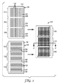
図1は、連続ウェビングに複数の液晶セル100を形成する2つの基材の例示的な積層体の概略的平面図である。例示の各基材は連続ウェビングの1区分であり、各区分は3つのセルを有する。各基材は、更に多い又は少ないセルを有することができ、多くの実施形態では、各連続ウェビングは、所望により、例えば10以上、25以上、50以上、又は100以上などの複数個のセルを有することが理解される。図2は、図1に示された例示的な積層体の概略的側面図であり、線2−2に沿って得られる概略的側面図である。各液晶セル区分100は、第1高分子基材130と第2高分子基材120との間に配置された液晶材料の層110を含む。
FIG. 1 is a schematic plan view of an exemplary laminate of two substrates forming a plurality of
第1高分子基材130は、複数個の第1平行導電トレース132を含み、これらのトレースは、第1方向に延びかつ液晶材料の層110と第1基材130との間に配置される。第1剥離ライナー150は、第1高分子基材130上に配置される。多くの実施形態では、複数個の第1平行導電トレース132は、複数個の個々の第1部分102に分割され、これらの部分は、第1トレース末端部及び対向する第2トレース末端部を有する。
The first
第2高分子基材120は、複数個の第2平行導電トレース122を含み、これらのトレースは、第1方向と直交する第2方向に延びかつ液晶材料の層110と第2基材120との間に配置される。多くの実施形態では、第2剥離ライナー140は、第2高分子基材120上に配置される。多くの実施形態では、複数個の第2平行導電トレース122は、第1トレース末端部及び対向する第2トレース末端部を有する、複数個の個々の第2部分101に分割される。幾つかの実施形態では、複数個の第2平行導電トレース122は、各セルを個片化することにより形成されるトレース末端部を有する連続線である。
The
第1高分子基材130は、液晶材料の層110の一部を露出させるために、第1剥離ライナー150と共に第1高分子基材130から分離できる、取り外し可能な部分134を更に含む。露出された液晶材料の層110の一部は、第2平行導電トレース122を露出させるために拭き取られる。取り外し可能な部分134は、取り外し可能なライナー150が残りの第1高分子基材130から分離すると、ライナー150と共に分離され、第1高分子基材130から離される。取り外し可能な部分134は、所定のスリット又は脆弱線135、例えば穿孔線などにより規定される。所定のスリット又は脆弱線135は、例えば、打抜き、レーザー切断などの、任意の有用な方法により形成され得る。
The first
図1に示されるような多くの実施形態では、第2高分子基材120は、液晶材料の層110の一部126を露出させるために、第2剥離ライナー140と共に第2高分子基材120から分離できる、取り外し可能な部分124を更に含む。露出された液晶材料の層110の一部126は、第1平行導電トレース132を露出させるために拭き取られ得る。取り外し可能な部分124は、取り外し可能なライナー140が残りの第2高分子基材120から分離すると、ライナー140と共に分離され、第2高分子基材120から離れる。取り外し可能な部分124は、所定のスリット又は脆弱線125、例えば、穿孔線などにより規定される。所定のスリット又は脆弱線125は、例えば、打抜き、レーザー切断、型押しなどの、任意の有用な方法により形成され得る。
In many embodiments, as shown in FIG. 1, the second
第1部分102及び第2部分101は、両者の間に配置された液晶層と共に位置合わせ及び積層されて、液晶セル部分103を形成する。取り外し可能な部分は、剥離ライナーと共に高分子基材から剥離され得て、液晶セル又はパッシブマトリクス液晶セルを形成する、反対側の高分子基材上の基層となる導電トレースにアクセスできるようにする。次に、各液晶セル部分103は、所望により、個片化されディスプレイデバイスに組み込むことができる。
The
前述の液晶セルの構成、及び後述の液晶セルの連続ウェビングを形成する方法は、導電リード線にアクセスする方法を提供し、連続ロール−ツーロールプロセスにおける様々なディスプレイ技術に使用され得る。本明細書に記載の構成及び方法の幾つかの利点には、積層後に正確な切込みを入れる方法に比べて、事前に切った部分を除去することで積層後の導電リード線にアクセスする方法の方が簡単であること、及び積層後に正確な切込みを入れる際に導電リード線を擦過又は破壊する危険性がないことが挙げられる。コーティング前に事前に切った窓を除去した場合、生じる空隙を埋めることで液晶コーティング材料を浪費するのを避けるために、事前に切った窓若しくは開口部、又は取り外し可能な部分を基材の定位置に維持したままにしておくことは、有利である。更に、事前に切った窓を定位置に残すことで、基材の厚さの急激な変化で起こり得るコーティングの中断を最小限に抑えられる。基材は、コーティング中に基材及び事前に切ったパターンの両方を共に維持する支持材料として働くライナーを背景に、事前に切ることができる。コーティングの完了後、続いて事前に切った窓の除去前又は除去と同時に、ライナーは剥離されることができる。液晶材料は、むき出しの導電リード線にアクセスできるよう、イソプロピルアルコール又はメタノールなどの適切な溶媒で拭き取ることにより、除去された窓の付近で取り除かれることができる。 The liquid crystal cell configuration described above and the method of forming a continuous webbing of the liquid crystal cell described below provide a way to access the conductive leads and can be used for various display technologies in a continuous roll-to-roll process. Some advantages of the arrangements and methods described herein include the ability to access the conductive leads after stacking by removing the pre-cut portions as compared to making precise cuts after stacking. It is simpler and there is no risk of scratching or destroying the conductive leads when making precise cuts after lamination. If pre-cut windows are removed before coating, pre-cut windows or openings, or removable parts, are defined on the substrate to avoid wasting liquid crystal coating material by filling the resulting voids. It is advantageous to keep it in position. In addition, leaving the pre-cut window in place minimizes coating interruptions that can occur with sudden changes in substrate thickness. The substrate can be pre-cut against a background of a liner that serves as a support material that maintains both the substrate and the pre-cut pattern during coating. After completion of the coating, the liner can then be peeled before or simultaneously with the removal of the pre-cut window. The liquid crystal material can be removed in the vicinity of the removed window by wiping with a suitable solvent such as isopropyl alcohol or methanol to provide access to the exposed conductive leads.
第1高分子基材130及び第2高分子基材120は、任意の有用な高分子材料から形成されることができる。多くの実施形態では、一方又は両方の高分子基材130及び120は、可視光線に対して透明であってもよい。多くの実施形態では、第1高分子基材130及び第2高分子基材120は、ロール−ツーロール装置で加工されるのに十分な機械的特性(例えば、強度及び可撓性)を有する好適な高分子材料から形成される。ロール−ツーロールは、材料が支持体に巻取られるか又は支持体から巻出され、加えて何らかの方法で更に加工されるプロセスを意味する。更なるプロセスの例としては、コーティング、スリット加工、打抜き加工、及び放射線への露出などが挙げられる。このようなポリマーの例としては、熱可塑性ポリマーが挙げられる。有用な熱可塑性ポリマーの例としては、ポリオレフィン、ポリアクリレート、ポリアミド、ポリイミド、ポリカーボネート、ポリエステル、及びビフェノール系又はナフタレン系の液晶ポリマーが挙げられる。有用な熱可塑性樹脂の更なる例としては、ポリエチレン、ポリプロピレン、ポリスチレン、ポリ(メチルメタクリレート)、ビスフェノールAのポリカーボネート、ポリ(塩化ビニル)、ポリエチレンテレフタレート、ポリエチレンナフタレート、及びポリ(フッ化ビニリデン)が挙げられる。これらのポリマーの一部は更に、特定のディスプレイ用途に特に良く適合する光学的特性(例えば、透明性)も有しており、それらがポリカーボネート、ポリイミド、及び/又はポリエステル等のパターン化された伝導体を支持する。
The
第1高分子基材130及び第2高分子基材120は、可撓性である。第1基材130及び第2基材120は、任意の有用な厚さを有することができる。これらの高分子基材130及び120は、一般に約5マイクロメートル〜1000マイクロメートル、又は25マイクロメートル〜500マイクロメートル、又は50マイクロメートル〜250マイクロメートル、又は75マイクロメートル〜200マイクロメートルの範囲の様々な厚さで作製することができる。
The
複数個の第1平行導電トレース132及び複数個の第2平行導電トレース122は、例えば、スパッタリング、化学蒸着などの、任意の有用な方法で形成されることができる。平行導電トレース132、122は、比較的導電性の透明なコーティングであることができる。多くの実施形態では、平行導電トレース132、122は、可視光線に対して透明である。平行導電トレース132、122は、酸化インジウムスズ、すなわちITOを含むことができ、ITOは、ITO伝導体の厚さに応じて、可視光線に対して透明であることができる。多くの実施形態では、平行導電トレース132、122は、概して均一な面積抵抗を有する。平行導電トレース132、122は、例えば、10〜100nmの厚さなど、任意の有用な厚さを有することができる。平行導電トレース132、122のパターンは、エンドユーザ用ディスプレイの寸法などの、ディスプレイの種類及び設計パラメーターにある程度依存してもよい。平行導電トレース132、122は、酸化アンチモンスズ、酸化亜鉛、又はその他の適切な導電材料を含むことができる。
The plurality of first parallel
液晶層110は、パッシブマトリクスディスプレイなどのディスプレイ用途に有用な任意の液晶から形成されることができる。多くの実施形態では、液晶層110は、コレステリック液晶から形成される。コレステリック液晶化合物には一般に、本質的にキラル(chiral)である分子単位(例えば、鏡面を持たない分子)、及び本質的にメソゲン(mesogenic)である分子単位(例えば、液晶相を呈する分子)が含まれるとともに、ポリマーであることができる。コレステリック液晶組成物は更に、キラル単位と混合した、すなわちキラル単位を含有する非キラル液晶化合物(ネマチック)を包含してもよい。コレステリック液晶組成物又は材料には、コレステリック液晶相を有する化合物が挙げられ、その相内では、その液晶のディレクタ(平均的な局所的分子整合方向を特定する単位ベクトル)がそのディレクタと直角をなす寸法に沿って螺旋状に回転する。コレステリック液晶組成物はまたキラルネマチック液晶組成物とも呼ばれている。コレステリック液晶組成物又は材料のピッチは、そのディレクタが360度回転するのに要する(そのディレクタと直角をなし、コレステリック螺旋軸に沿った方向の)距離である。この距離は一般に、100nm以上である。
The
コレステリック液晶材料のピッチは、キラル化合物をネマチック液晶化合物と混合させるか、さもなければそれらを組み合せる(例えば、共重合によって)ことにより生じさせることができる。コレステリック相は、キラル非液晶材によっても生じさせることができる。ピッチは、キラル化合物とネマチック液晶化合物又は材料との相対重量比に左右されると思われる。そのディレクタの螺旋のねじれが、当該材料の誘電テンソルの空間的な周期的変動をひき起し、その結果として光の波長選択的な反射を生じさせる。例えば、ピッチは、そのブラッグ反射が光の可視波長領域、紫外線波長領域、又は赤外線波長領域においてピークとなるように選択することができる。 The pitch of the cholesteric liquid crystal material can be generated by mixing a chiral compound with a nematic liquid crystal compound or otherwise combining them (eg, by copolymerization). The cholesteric phase can also be generated by chiral non-liquid crystal materials. The pitch appears to depend on the relative weight ratio between the chiral compound and the nematic liquid crystal compound or material. The director's helical twist causes spatially periodic variations in the dielectric tensor of the material, resulting in wavelength selective reflection of light. For example, the pitch can be selected such that the Bragg reflection peaks in the visible wavelength region, ultraviolet wavelength region, or infrared wavelength region of light.
コレステリック液晶ポリマーを含むコレステリック液晶化合物が一般に知られており、典型的にはこれら材料のうちどれを用いても光学体を作製することができる。好適なコレステリック液晶ポリマーの例は、米国特許第4,293,435号、同第5,332,522号、同第5,886,242号、同第5,847,068号、同第5,780,629号、同第5,744,057号に記載されており、これら全てを参照によって本明細書に組み込む。また、他のコレステリック液晶化合物も用いることができる。コレステリック液晶化合物は、1つ以上の要因に基づいて、ある特定の用途又は光学体に適合するように選択されてもよく、例えば、その要因とは、屈折率、表面エネルギー、ピッチ、加工性、透明度、色、問題となる波長における低い吸収、他の構成成分(例えば、ネマチック液晶化合物等)との相溶性、分子量、作製し易さ、液晶ポリマーを形成する液晶化合物又はモノマーの入手可能性、レオロジー、硬化方法及び硬化要件、溶媒の除去し易さ、物理的及び化学的性質(例えば、可撓性、引張強さ、耐溶剤性、引っかき抵抗、及び相転移温度)、並びに精製し易さを含む。 Cholesteric liquid crystal compounds including cholesteric liquid crystal polymers are generally known, and typically any of these materials can be used to make optical bodies. Examples of suitable cholesteric liquid crystal polymers include U.S. Pat. Nos. 4,293,435, 5,332,522, 5,886,242, 5,847,068, 780,629, 5,744,057, all of which are incorporated herein by reference. Other cholesteric liquid crystal compounds can also be used. The cholesteric liquid crystal compound may be selected to suit a particular application or optical body based on one or more factors, such as refractive index, surface energy, pitch, processability, Transparency, color, low absorption at the wavelength in question, compatibility with other components (eg nematic liquid crystal compounds, etc.), molecular weight, ease of preparation, availability of liquid crystal compounds or monomers forming liquid crystal polymers, Rheology, cure method and requirements, ease of solvent removal, physical and chemical properties (eg, flexibility, tensile strength, solvent resistance, scratch resistance, and phase transition temperature), and ease of purification including.
多くの実施形態では、コレステリック液晶層は、高分子マトリクス(連続相)内に分散された液晶相(分散相)を含む、高分子分散型液晶組成物である。多くの実施形態では、高分子分散型液晶組成物は、重合誘導相分離(PIPS)によって形成され、形成される液晶相の液滴の大きさは、重合反応速度によって少なくとも部分的に制御される。 In many embodiments, the cholesteric liquid crystal layer is a polymer dispersed liquid crystal composition comprising a liquid crystal phase (dispersed phase) dispersed in a polymer matrix (continuous phase). In many embodiments, the polymer dispersed liquid crystal composition is formed by polymerization induced phase separation (PIPS), and the size of the liquid crystal phase droplets formed is at least partially controlled by the polymerization reaction rate. .
多くの実施形態では、この構造体は、双安定反射型コレステリック液晶ディスプレイ又はパッシブマトリクスディスプレイを形成する。平行導電トレース132、122全体に電界(E)を適用すると、液晶は、反射する平面状態又は散乱する焦点円錐状態のいずれかに整列する。これらの状態はいずれも、E=0では安定であり、それ故に構造は固定されており、再度作用を受けるまで元の状態のままである(すなわち、デバイスは双安定性である)。平面状態から焦点円錐状態への切り替えには低電圧のパルスが必要である一方で、焦点円錐状態から平面状態へ戻るのには高電圧のパルスが必要であって、デバイスをホメオトロピック状態とした後、最終的な平面状態に弛緩する。単一ピクセルのコレステリック液晶ディスプレイ(すなわち、ChLCD)セルを切り替えるための例示的な駆動スキームは、デン−キー・ヤン(Deng-Ke Ynag)他によって記載されている(材料科学の年報(Annu. Rev. Mater. Sci.)、1977年、27巻、117〜146頁)。この文献に記載の反射率対電圧のプロットに従って、ChLCDセルを、セルが平面状態のときの電圧値、又はセルが焦点円錐状態のときの電圧値に切り替えることができる。関連したパルス列(周波数及び振幅)は、当業者であれば誰でも実施可能である。
In many embodiments, this structure forms a bistable reflective cholesteric liquid crystal display or passive matrix display. When an electric field (E) is applied across the parallel
代表的な液晶組成物は、2007年11月8日に出願された係属中の米国特許出願公開第11/557,540号(代理人整理番号62381US002号)に記載されており、その開示内容は参照により本明細書に組み込まれ、その開示内容は対応する安定な平面状態の反射を提供する。安定な状態の反射とは、セルが電圧によって平面状態になってから、周囲条件下に約3日間置かれた後で反射損失を呈さないことを意味する。 A typical liquid crystal composition is described in pending U.S. Patent Application Publication No. 11 / 557,540 (Attorney Docket No. 62381 US002) filed on Nov. 8, 2007. Incorporated herein by reference, the disclosure provides a corresponding stable planar state reflection. Stable reflection means that the cell does not exhibit reflection loss after being brought to a planar state by voltage and after being placed under ambient conditions for about 3 days.
液晶層110は、例えば、1〜15マイクロメートルの範囲の厚さなど、任意の有用な厚さを有することができる。1〜15マイクロメートルの範囲の厚さを有するこの高分子分散型液晶層110は、0.1〜10mW/cm2の範囲、又は0.2〜3mW/cm2の範囲の放射線硬化によって形成することができる。
The
高分子分散型液晶層110は、反応性プレポリマー/液晶組成物を混合して重合するプロセスで形成されることができる。多くの実施形態では、反応性プレポリマー/液晶組成物は単相を形成し、ここで液晶は重合しない。組成物が重合すると、ポリマーは液晶から分離して、液晶が、高分子マトリクス内に分散された液晶ドメイン(例えば、液滴)を形成する。この相分離プロセスは、重合誘導相分離(すなわち、PIPS)と称される。PIPSプロセスでは、ポリマー相は、ポリマーの長さが増加するにつれて、重合中に液晶相から分離する。反応性プレポリマー/液晶組成物は、液晶構成成分、光重合開始剤及びポリマー前駆体構成成分を含む。これら構成成分は、プレポリマー/液晶組成物が重合するまで単相を形成するように選択される。
The polymer dispersed
液晶構成成分は、例えば、コレステリック液晶材料又はネマチック液晶材料等の、いずれかの有用な液晶であり得る。液晶は、組成物中に任意の有用な量で存在することができる。多くの実施形態では、液晶は、組成物中に60〜95重量%、又は70〜95重量%の範囲で存在することができる。 The liquid crystal component can be any useful liquid crystal such as, for example, a cholesteric liquid crystal material or a nematic liquid crystal material. The liquid crystal can be present in any useful amount in the composition. In many embodiments, the liquid crystal can be present in the composition in the range of 60-95 wt%, or 70-95 wt%.
光重合開始剤は、任意の有用な光重合開始剤であってよい。多くの実施形態では、光開始剤としては、ヒドロキシ−アルキルベンゾフェノン(例えば、メルク(Merck)から入手可能なダロキュア(Darocur)(登録商標))、ベンゾインエーテル、アルキルフェノン、ベンゾフェノン、キサントン、チオキサントン、ホスフィンオキシド(例えば、チバ・スペシャルティ・ケミカルズ(Ciba Specialty Chemicals)から入手可能なイルガキュア(Irgacure)(登録商標)819)、及びそれらの派生品が挙げられる。追加の有用な光重合開始剤は、米国特許第5,516,455号に記載されており、これを本開示内容と矛盾しない範囲まで、参照により組み込む。光重合開始剤は、組成物中に任意の有用な量で存在することができる。多くの実施形態では、光重合開始剤は、0.01〜10重量%、又は0.1〜5重量%、又は1〜2重量%の範囲で存在することができる。 The photopolymerization initiator may be any useful photopolymerization initiator. In many embodiments, the photoinitiator includes a hydroxy-alkyl benzophenone (eg, Darocur® available from Merck), a benzoin ether, an alkylphenone, a benzophenone, a xanthone, a thioxanthone, a phosphine. Oxides (eg, Irgacure® 819 available from Ciba Specialty Chemicals), and derivatives thereof. Additional useful photoinitiators are described in US Pat. No. 5,516,455, which is incorporated by reference to the extent it does not conflict with the present disclosure. The photoinitiator can be present in any useful amount in the composition. In many embodiments, the photoinitiator can be present in the range of 0.01 to 10 wt%, or 0.1 to 5 wt%, or 1-2 wt%.
幾つかの実施形態では、液晶層110は、高分子基材間に均一な間隔を提供するのに役立つ空間用ビーズ(図示なし)を含む。
In some embodiments, the
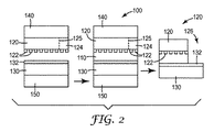
図3は、前述の連続ウェビングに複数の液晶セルを形成するための例示的なロール−ツーロール積層プロセス200の概略図である。装置200は、第1方向に延びる第1平行導電トレース232を複数有するウェビング230すなわち連続高分子基材用の第1ロール202と、第1方向と直交する第2方向に延びる第2平行導電トレース222を複数有するウェビング220すなわち連続高分子基材用の第2ロール201と、を含む。多くの実施形態では、複数個の第1平行導電トレース232及び複数個の第2平行導電トレース222は、前述したように複数個の個別の部分に分割されている。連続高分子基材すなわちウェビング230用の第1ロール202は、第1剥離ライナー250を含み、連続高分子基材すなわちウェビング220用の第2ロール201は、第2剥離ライナー240を含む。
FIG. 3 is a schematic diagram of an exemplary roll-to-
装置200は、第1及び第2ウェビング230、220に付随する第1及び第2切断装置233、223を含む。切断装置233、223は、ウェビングの積層後に、対向するウェビングの導電トレース末端部(前述)に相当する所定の位置で、第1及び第2ウェビング230、220の切断、型押し、又は穿孔(前述)を行う。切断装置233、223は、第1及び第2ウェビング230、220の積層後にライナー250、240と共に取り除かれるウェビングの取り外し可能な部分234、224(前述)を形成する。
The
装置200は、ニップポイント(nip point)206を規定する一対のニップローラー(nip roller)205を含む。ニップローラーは、ニップポイント206に向けて第1及び第2ウェビング230、220を移動させ、そこで、液晶ディスペンサー210が、液晶材料を分配し、第1ウェビング230と第2ウェビング220との間に液晶材料を積層させ、液晶セルウェビング207を形成する。
The
液晶セルウェビング207は、硬化用エレメント260により硬化され、剥離ライナー250、240は、液晶セルウェビング207から取り除くことができる。幾つかの実施形態では、液晶セルウェビング207が硬化用エレメント260により硬化された後、剥離ライナー250、240が液晶セルウェビング207から取り除かれる。別の実施形態では、剥離ライナー250、240が液晶セルウェビング207から取り除かれた後、液晶セルウェビング207が硬化用エレメント260により硬化される。取り外し可能な部分234、224は、液晶セル又はパッシブマトリクス液晶セルを形成する反対側の高分子基材上の、基層となる導電トレースにアクセスできるように、剥離ライナー250、240と共に取り除かれる。液晶セル連続ウェビング207は、製品ロール203上に置かれてもよく、及び/又は前述したように、各液晶セル部分は、個片化され、ディスプレイデバイスに組み立てられてもよい。
The liquid
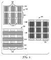
図5は、連続ウェビングに複数の液晶セル300を形成する2つの基材の別の例示的な積層体の概略的平面図である。例示の各基材は連続ウェビングの一区分であり、各区分は9つのセル、すなわち3×3の区分を有する。各基材は、任意の配置で更に多い又は少ないセルを有することができ、多くの実施形態では、各連続ウェビングは、所望により、例えば、10以上、25以上、50以上、又は100以上などの複数個のセルを有することが理解される。各液晶セル区分300は、前述したように、第1高分子基材330と第2高分子基材320との間に配置された液晶材料の層を含む。
FIG. 5 is a schematic plan view of another exemplary laminate of two substrates that form a plurality of
第1高分子基材330は、第1方向に延びかつ液晶材料の層と第1基材330との間に配置された、複数個の第1平行導電トレース332を含む。前述の第1剥離ライナーは、第1高分子基材330上に配置される。多くの実施形態では、複数個の第1平行導電トレース332は、第1トレース末端部及び対向する第2トレース末端部を有する複数個の個々の第1部分302に分割される。幾つかの実施形態では、複数個の第2平行導電トレース332は、各セル303を個片化することにより形成されるトレース末端部を有する連続線である。
The first
第2高分子基材320は、第1方向と直交する第2方向に延びかつ液晶材料の層と第2基材320との間に配置された、複数個の第2平行導電トレース322を含む。多くの実施形態では、第2剥離ライナーは、第2高分子基材320上に配置される。多くの実施形態では、複数個の第2平行導電トレース322は、第1トレース末端部及び対向する第2トレース末端部を有する複数個の個々の第2部分301に分割される。幾つかの実施形態では、複数個の第2平行導電トレース322は、各セル303を個片化することにより形成されるトレース末端部を有する連続線である。
The
第1高分子基材330は、液晶材料の層の一部を露出させるために第1剥離ライナー(前述)と共に第1高分子基材330から分離できる、取り外し可能な部分334を更に含み、露出された液晶材料の層の一部は、第2平行導電トレース322を露出させるために拭き取られ得る。取り外し可能な部分334は、前述したように、取り外し可能なライナー350が残りの第1高分子基材330から分離すると、ライナーと共に分離され、第1高分子基材330から離される。取り外し可能な部分334は、所定のスリット又は脆弱線、例えば穿孔線などにより規定される。所定のスリット又は脆弱線は、例えば、打抜き、レーザー切断などの、任意の有用な方法により形成され得る。
The first
図5に示すような多くの実施形態では、第2高分子基材320は、前述したように、液晶材料の層の一部を露出させるために第2剥離ライナーと共に第2高分子基材320から分離できる、取り外し可能な部分324を更に含み、この取り外し可能な部分は、第1平行導電トレース332を露出させるために拭き取られ得る。取り外し可能な部分324は、前述したように、取り外し可能なライナーが残りの第2高分子基材320から分離すると、ライナーと共に第2高分子基材320から分離され、離される。取り外し可能な部分324は、所定のスリット又は脆弱線、例えば穿孔線などにより規定される。所定のスリット又は脆弱線は、例えば、打抜き、レーザー切断、型押しなどの、任意の有用な方法により形成され得る。
In many embodiments, such as that shown in FIG. 5, the second
第1部分302及び第2部分301は、両者の間に配置された液晶層と共に位置合わせ及び積層されて、液晶セル部分303を形成する。取り外し可能な部分は、液晶セル又はパッシブマトリクス液晶セルを形成する反対側の高分子基材上の、基層となる導電トレースにアクセスできるよう、剥離ライナーと共に高分子基材から剥離され得る。次に、各液晶セル部分303は、所望により、個片化され、ディスプレイデバイスに組み立てられることができる。
The
前述の液晶セルの構成、及び前述の液晶セルの連続ウェビングを形成する方法は、導電リード線にアクセスする方法を提供し、連続ロール−ツーロールプロセスにおける様々なディスプレイ技術に使用され得る。 The configuration of the liquid crystal cell described above and the method of forming the continuous webbing of the liquid crystal cell described above provide a way to access the conductive leads and can be used for various display technologies in a continuous roll-to-roll process.
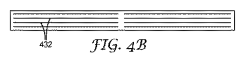
図4A及び4Bに示されるように、ITOの横列及び縦列を、61cm(24インチ)幅で127マイクロメートル(5ミル)のデュポン・テイジン(Dupont Teijin)ST−504ポリエチレンテレフタレートフィルム上にパターン形成した。このウェブは、縦列パターン(図4AのクロスウェブITO線422)を有する15.2cm(6インチ)幅の2つの幅と、横列パターン(図4BのダウンウェブITO線432)を有する10.8cm(4.25インチ)幅の2つの幅との、4つの幅にスリットが入れられた。2つの15.2cm(6インチ)幅のロール(図4A)には、透明なライナーが非ITO側に積層された。窓424を、基材の縦列パターン間に回転させて打抜きした。各窓424の寸法は、約8.9cm(3.5インチ)×10.2cm(4インチ)であった。窓424は、透明な支持ライナー上で基材の残りと共に所定の位置に残った。
4A and 4B, ITO rows and columns were patterned on a 61 cm (24 inch) wide 127 micrometer (5 mil) Dupont Teijin ST-504 polyethylene terephthalate film. . The web has two widths of 15.2 cm (6 inches) wide with a column pattern (
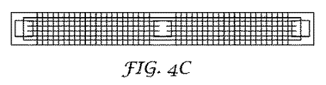
この打抜きした15.2cm(6インチ)の縦列パターンウェビング(図4A)を、下部基材としてロール−ツーロール装置に配置した。幅が狭い方の10.8cm(4.25インチ)の横列パターンウェビング(図4B)を、上部基材としてロール−ツーロール装置に配置した。図4Cは、基材を配列した状態の概略的平面図を示す。 This punched 15.2 cm (6 inch) column pattern webbing (FIG. 4A) was placed in a roll-to-roll apparatus as the lower substrate. The narrower 10.8 cm (4.25 inch) row pattern webbing (FIG. 4B) was placed in a roll-to-roll apparatus as the top substrate. FIG. 4C shows a schematic plan view of the substrate arranged.
2つの基材はニッププロセス(nip process)で合わせられ、このプロセスで、コレステリック液晶コーティング溶液が基材間に分配され、続いて硬化され、ロール−ツーロール装置の末端部でシート化された。次に、ライナーが縦列の基材の裏側から取り除かれ、事前に切った窓もライナーと共に取り除かれた。窓を取り除いた後、窓があった部分の下の領域をアルコールで拭き取ることにより、むき出しの電気接点が露出される。 The two substrates were combined in a nip process, in which the cholesteric liquid crystal coating solution was dispensed between the substrates and subsequently cured and sheeted at the end of a roll-to-roll apparatus. The liner was then removed from the back of the column of substrates and the pre-cut windows were removed with the liner. After removing the window, the bare electrical contacts are exposed by wiping the area under the window with alcohol.
上に述べたように、「液晶ディスプレイパネル及びその製造方法」の実施形態が開示された。本発明が、開示されたもの以外の実施形態で実施され得ることは、当業者には理解されよう。開示された実施形態は、例証の目的で提示されているのであって、制限するものではなく、本発明は、以降に続く請求項によってのみ限定される。 As described above, the embodiment of “Liquid Crystal Display Panel and Method for Manufacturing the Same” has been disclosed. Those skilled in the art will appreciate that the invention may be practiced with embodiments other than those disclosed. The disclosed embodiments are presented for purposes of illustration and not limitation, and the invention is limited only by the claims that follow.
Claims (20)
前記第1高分子基材が、第1方向に延びかつ前記液晶材料の層と前記第1基材との間に配置された複数個の第1平行導電トレースと、前記第1高分子基材上に配置された第1剥離ライナーとを含み、
前記第2高分子基材が、前記第1方向と直交する第2方向に延びかつ前記液晶材料の層と前記第2基材との間に配置された、複数個の第2平行導電トレースを含み、
前記第1高分子基材が、前記液晶材料の層又は前記第2平行導電トレースの一部を露出させるために前記第1剥離ライナーと共に前記第1高分子基材から分離できる、取り外し可能な部分を更に含む、液晶セル物品。 A liquid crystal cell article comprising a layer of liquid crystal material disposed between a first polymer substrate and a second polymer substrate,
A plurality of first parallel conductive traces extending in a first direction and disposed between the liquid crystal material layer and the first substrate; and the first polymer substrate. A first release liner disposed on the top,
A plurality of second parallel conductive traces, wherein the second polymer substrate extends in a second direction orthogonal to the first direction and is disposed between the liquid crystal material layer and the second substrate; Including
A removable portion wherein the first polymeric substrate can be separated from the first polymeric substrate with the first release liner to expose a layer of the liquid crystal material or a portion of the second parallel conductive trace. A liquid crystal cell article further comprising:
第1高分子基材と第2高分子基材との間に配置された液晶材料の層と、
第1方向に延び、かつ前記液晶材料の層と前記第1基材との間に配置された、複数個の第1平行導電トレースと、前記第1高分子基材上に配置された第1剥離ライナーとを含み、取り外し可能な部分を更に含む、前記第1高分子基材と、
前記第1方向と直交する第2方向に延び、かつ前記液晶材料の層と前記第2基材との間に配置された、複数個の第2平行導電トレースを含む、前記第2高分子基材と、を含む液晶セル物品を、提供する工程と、
前記液晶材料の層の一部又は前記第2平行導電トレースの一部を露出させるために前記第1剥離ライナー及び前記取り外し可能な部分を分離する工程と、
を含む、方法。 A method of manufacturing a liquid crystal cell, comprising:
A layer of liquid crystal material disposed between the first polymer substrate and the second polymer substrate;
A plurality of first parallel conductive traces extending in a first direction and disposed between the layer of liquid crystal material and the first substrate, and a first disposed on the first polymer substrate. Said first polymeric substrate comprising a release liner and further comprising a removable portion;
The second polymeric group comprising a plurality of second parallel conductive traces extending in a second direction orthogonal to the first direction and disposed between the layer of liquid crystal material and the second substrate. Providing a liquid crystal cell article comprising:
Separating the first release liner and the removable portion to expose a portion of the layer of liquid crystal material or a portion of the second parallel conductive trace;
Including a method.
液晶セルを形成する第1高分子基材と第2高分子基材との間に液晶材料の層を配置する工程であって、
前記第1高分子基材が、第1方向に延びかつ前記液晶材料の層と前記第1基材との間に配置された複数個の第1平行導電トレースと、前記第1高分子基材上に配置された第1剥離ライナーとを含み、前記第1高分子基材が、取り外し可能な部分を更に含み、かつ
前記第2高分子基材が、前記第1方向と直交する第2方向に延びかつ前記液晶材料の層と前記第2基材との間に配置された複数個の第2平行導電トレースを含む、配置工程と、
前記液晶材料の層の一部又は前記第2平行導電トレースの一部を露出させるために前記第1剥離ライナー及び前記取り外し可能な部分を分離する工程と、を含む製造方法。 A method of manufacturing a liquid crystal cell, comprising:
Disposing a layer of liquid crystal material between a first polymer substrate and a second polymer substrate forming a liquid crystal cell,
A plurality of first parallel conductive traces extending in a first direction and disposed between the liquid crystal material layer and the first substrate; and the first polymer substrate. A first release liner disposed on the first polymeric substrate, wherein the first polymeric substrate further includes a removable portion, and the second polymeric substrate is in a second direction orthogonal to the first direction. A plurality of second parallel conductive traces extending between and disposed between the layer of liquid crystal material and the second substrate;
Separating the first release liner and the removable portion to expose a portion of the layer of liquid crystal material or a portion of the second parallel conductive trace.
Applications Claiming Priority (2)
| Application Number | Priority Date | Filing Date | Title |
|---|---|---|---|
| US11/768,283 US8089604B2 (en) | 2007-06-26 | 2007-06-26 | Liquid crystal display panel and methods of manufacturing the same |
| PCT/US2008/064936 WO2009002647A2 (en) | 2007-06-26 | 2008-05-28 | Liquid crystal display panel and methods of manufacturing the same |
Publications (2)
| Publication Number | Publication Date |
|---|---|
| JP2010532016A true JP2010532016A (en) | 2010-09-30 |
| JP2010532016A5 JP2010532016A5 (en) | 2011-07-14 |
Family
ID=40159970
Family Applications (1)
| Application Number | Title | Priority Date | Filing Date |
|---|---|---|---|
| JP2010514918A Withdrawn JP2010532016A (en) | 2007-06-26 | 2008-05-28 | Liquid crystal display panel and manufacturing method thereof |
Country Status (6)
| Country | Link |
|---|---|
| US (1) | US8089604B2 (en) |
| EP (1) | EP2171533A4 (en) |
| JP (1) | JP2010532016A (en) |
| KR (1) | KR20100041774A (en) |
| CN (1) | CN101688999A (en) |
| WO (1) | WO2009002647A2 (en) |
Families Citing this family (3)
| Publication number | Priority date | Publication date | Assignee | Title |
|---|---|---|---|---|
| US8817360B2 (en) | 2008-03-05 | 2014-08-26 | Hitachi Chemical Company, Ltd. | Method for producing light-modulating film and light-modulating film |
| US8599353B2 (en) | 2010-05-28 | 2013-12-03 | 3M Innovative Properties Company | Display comprising a plurality of substrates and a plurality of display materials disposed between the plurality of substrates that are connected to a plurality of non-overlapping integral conductive tabs |
| CN102517039A (en) * | 2011-10-25 | 2012-06-27 | 珠海彩珠实业有限公司 | A kind of preparation method of liquid crystal alignment agent, liquid crystal alignment film and liquid crystal cell |
Family Cites Families (22)
| Publication number | Priority date | Publication date | Assignee | Title |
|---|---|---|---|---|
| DE2831909A1 (en) | 1978-07-20 | 1980-02-07 | Basf Ag | LIQUID CRYSTALLINE POLYMER PHASE WITH CHOLESTERIC STRUCTURE, METHOD FOR THE PRODUCTION THEREOF AND THEIR USE |
| JPS58181022A (en) | 1982-04-16 | 1983-10-22 | Sharp Corp | Manufacturing method of flexible display element |
| US5332522A (en) | 1993-04-29 | 1994-07-26 | The University Of Rochester | Thermotropic chiral nematic liquid crystalline copolymers |
| WO1994025508A1 (en) | 1993-05-03 | 1994-11-10 | Loctite Corporation | Polymer dispersed liquid crystals in electron-rich alkene-thiol polymers |
| DE4342280A1 (en) | 1993-12-11 | 1995-06-14 | Basf Ag | Polymerizable chiral compounds and their use |
| DE19520704A1 (en) | 1995-06-09 | 1996-12-12 | Basf Ag | Polymerizable chiral compounds and their use |
| US5847068A (en) | 1997-04-03 | 1998-12-08 | Basf Aktiengesellschaft | Cholesteric copolyisocyanates |
| JP3746925B2 (en) * | 1999-08-27 | 2006-02-22 | セイコーエプソン株式会社 | Liquid crystal device and electronic device |
| JP2002023128A (en) | 2000-07-06 | 2002-01-23 | Minolta Co Ltd | Method for manufacturing liquid crystal display element and method for manufacturing hollow liquid crystal display element |
| JP3980817B2 (en) | 2000-08-02 | 2007-09-26 | 株式会社リコー | Manufacturing method of liquid crystal display device and manufacturing apparatus used therefor |
| TW574538B (en) | 2002-04-24 | 2004-02-01 | Sipix Imaging Inc | Compositions and processes for format flexible roll-to-roll manufacturing of electrophoretic displays |
| TW583497B (en) | 2002-05-29 | 2004-04-11 | Sipix Imaging Inc | Electrode and connecting designs for roll-to-roll format flexible display manufacturing |
| US6897099B2 (en) | 2002-07-23 | 2005-05-24 | Lg. Philips Lcd Co., Ltd. | Method for fabricating liquid crystal display panel |
| JP3871983B2 (en) | 2002-08-08 | 2007-01-24 | 鹿児島日本電気株式会社 | Manufacturing method of liquid crystal display panel |
| US6831712B1 (en) * | 2003-05-27 | 2004-12-14 | Eastman Kodak Company | Polymer-dispersed liquid-crystal display comprising an ultraviolet blocking layer and methods for making the same |
| TWI228190B (en) | 2003-09-29 | 2005-02-21 | Ind Tech Res Inst | Method of fabricating a passive matrix plastic display by roll-to-roll process |
| KR100689314B1 (en) | 2003-11-29 | 2007-03-08 | 엘지.필립스 엘시디 주식회사 | Cutting Method of LCD Panel |
| KR20050082449A (en) | 2004-02-19 | 2005-08-24 | 소프트픽셀(주) | Cell cutting method for plastic film lcd and apparatus thereof |
| WO2006011695A1 (en) | 2004-07-30 | 2006-02-02 | Si-Han Kim | Method for making electrode terminal of panel using polymer and liquid crystal compound |
| KR100692695B1 (en) * | 2004-11-30 | 2007-03-14 | 비오이 하이디스 테크놀로지 주식회사 | LCD Display |
| US20060137813A1 (en) | 2004-12-29 | 2006-06-29 | Robrecht Michael J | Registered lamination of webs using laser cutting |
| US7745733B2 (en) | 2005-05-02 | 2010-06-29 | 3M Innovative Properties Company | Generic patterned conductor for customizable electronic devices |
-
2007
- 2007-06-26 US US11/768,283 patent/US8089604B2/en not_active Expired - Fee Related
-
2008
- 2008-05-28 EP EP08756344A patent/EP2171533A4/en not_active Withdrawn
- 2008-05-28 WO PCT/US2008/064936 patent/WO2009002647A2/en not_active Ceased
- 2008-05-28 CN CN200880021676A patent/CN101688999A/en active Pending
- 2008-05-28 KR KR1020107001287A patent/KR20100041774A/en not_active Withdrawn
- 2008-05-28 JP JP2010514918A patent/JP2010532016A/en not_active Withdrawn
Also Published As
| Publication number | Publication date |
|---|---|
| EP2171533A2 (en) | 2010-04-07 |
| CN101688999A (en) | 2010-03-31 |
| WO2009002647A2 (en) | 2008-12-31 |
| US8089604B2 (en) | 2012-01-03 |
| WO2009002647A3 (en) | 2009-02-12 |
| US20090002622A1 (en) | 2009-01-01 |
| EP2171533A4 (en) | 2011-04-06 |
| KR20100041774A (en) | 2010-04-22 |
Similar Documents
| Publication | Publication Date | Title |
|---|---|---|
| EP2697684B1 (en) | Transparent electrode for electronic displays | |
| TW548326B (en) | Cholesteric liquid crystal optical bodies and methods of manufacture and use | |
| US20060204675A1 (en) | Display device with improved flexibility | |
| TWI292492B (en) | ||
| CN104995218A (en) | polymerizable composition | |
| TW200728084A (en) | Infrared light reflecting film | |
| JP2003121641A (en) | Laminated retardation plate, polarizing member and liquid crystal display | |
| US20220082885A1 (en) | Polarizing substrate and variable transmissivity device including the polarizing substrate | |
| CN115335222B (en) | Laminate for transferring thin film layer | |
| JP6965605B2 (en) | Dimming film | |
| US11143898B2 (en) | Multicolor liquid crystal writing device | |
| JP2010532016A (en) | Liquid crystal display panel and manufacturing method thereof | |
| WO2005092755A1 (en) | Continuous support interleaving | |
| US7202097B2 (en) | Light polarizing film, a method of continuously fabricating same, and reflective optical film using same | |
| CN100417956C (en) | Polarizing optical element, manufacturing method thereof, and reflective optical element using the same | |
| JP2024525388A (en) | Optical laminate and its manufacturing method, smart window including the same, and automobile and building fittings using the same | |
| JP2019174636A (en) | Oblique stretched film, polarizer, irregular shaped display and method for manufacturing oblique stretched film | |
| JP2018112699A (en) | Long-sized dimming device | |
| WO2022186387A1 (en) | Light control sheet and light control device | |
| US20250053047A1 (en) | Liquid crystal element and liquid crystal element production method | |
| CN120295027A (en) | Optical laminate and method for producing the same, smart window containing the same, and automobile or building window using the same | |
| US20250264766A1 (en) | Optical laminate, smart window including the same, and automobile or window for building using the same | |
| EP4538785A1 (en) | Optical laminate, method for manufacturing same, and smart window comprising same | |
| CN120044723A (en) | Optical laminate, method for producing same, smart window comprising same, and window for automobile or building using same | |
| CN120044722A (en) | Optical laminate, method for producing same, smart window comprising same, and window for automobile or building using same |
Legal Events
| Date | Code | Title | Description |
|---|---|---|---|
| A521 | Request for written amendment filed |
Free format text: JAPANESE INTERMEDIATE CODE: A523 Effective date: 20110524 |
|
| A621 | Written request for application examination |
Free format text: JAPANESE INTERMEDIATE CODE: A621 Effective date: 20110524 |
|
| A761 | Written withdrawal of application |
Free format text: JAPANESE INTERMEDIATE CODE: A761 Effective date: 20110707 |