JP2010531044A - Insulating paste for metal core substrates and electronic devices - Google Patents
Insulating paste for metal core substrates and electronic devices Download PDFInfo
- Publication number
- JP2010531044A JP2010531044A JP2010513404A JP2010513404A JP2010531044A JP 2010531044 A JP2010531044 A JP 2010531044A JP 2010513404 A JP2010513404 A JP 2010513404A JP 2010513404 A JP2010513404 A JP 2010513404A JP 2010531044 A JP2010531044 A JP 2010531044A
- Authority
- JP
- Japan
- Prior art keywords
- glass
- paste
- insulating
- metal core
- insulating layer
- Prior art date
- Legal status (The legal status is an assumption and is not a legal conclusion. Google has not performed a legal analysis and makes no representation as to the accuracy of the status listed.)
- Withdrawn
Links
Images


Classifications
-
- C—CHEMISTRY; METALLURGY
- C03—GLASS; MINERAL OR SLAG WOOL
- C03C—CHEMICAL COMPOSITION OF GLASSES, GLAZES OR VITREOUS ENAMELS; SURFACE TREATMENT OF GLASS; SURFACE TREATMENT OF FIBRES OR FILAMENTS MADE FROM GLASS, MINERALS OR SLAGS; JOINING GLASS TO GLASS OR OTHER MATERIALS
- C03C8/00—Enamels; Glazes; Fusion seal compositions being frit compositions having non-frit additions
- C03C8/02—Frit compositions, i.e. in a powdered or comminuted form
-
- C—CHEMISTRY; METALLURGY
- C03—GLASS; MINERAL OR SLAG WOOL
- C03C—CHEMICAL COMPOSITION OF GLASSES, GLAZES OR VITREOUS ENAMELS; SURFACE TREATMENT OF GLASS; SURFACE TREATMENT OF FIBRES OR FILAMENTS MADE FROM GLASS, MINERALS OR SLAGS; JOINING GLASS TO GLASS OR OTHER MATERIALS
- C03C8/00—Enamels; Glazes; Fusion seal compositions being frit compositions having non-frit additions
- C03C8/14—Glass frit mixtures having non-frit additions, e.g. opacifiers, colorants, mill-additions
- C03C8/20—Glass frit mixtures having non-frit additions, e.g. opacifiers, colorants, mill-additions containing titanium compounds; containing zirconium compounds
-
- H—ELECTRICITY
- H01—ELECTRIC ELEMENTS
- H01L—SEMICONDUCTOR DEVICES NOT COVERED BY CLASS H10
- H01L23/00—Details of semiconductor or other solid state devices
- H01L23/12—Mountings, e.g. non-detachable insulating substrates
- H01L23/14—Mountings, e.g. non-detachable insulating substrates characterised by the material or its electrical properties
- H01L23/142—Metallic substrates having insulating layers
-
- H—ELECTRICITY
- H01—ELECTRIC ELEMENTS
- H01L—SEMICONDUCTOR DEVICES NOT COVERED BY CLASS H10
- H01L23/00—Details of semiconductor or other solid state devices
- H01L23/48—Arrangements for conducting electric current to or from the solid state body in operation, e.g. leads, terminal arrangements ; Selection of materials therefor
- H01L23/488—Arrangements for conducting electric current to or from the solid state body in operation, e.g. leads, terminal arrangements ; Selection of materials therefor consisting of soldered or bonded constructions
- H01L23/498—Leads, i.e. metallisations or lead-frames on insulating substrates, e.g. chip carriers
- H01L23/49866—Leads, i.e. metallisations or lead-frames on insulating substrates, e.g. chip carriers characterised by the materials
- H01L23/49894—Materials of the insulating layers or coatings
-
- H—ELECTRICITY
- H05—ELECTRIC TECHNIQUES NOT OTHERWISE PROVIDED FOR
- H05K—PRINTED CIRCUITS; CASINGS OR CONSTRUCTIONAL DETAILS OF ELECTRIC APPARATUS; MANUFACTURE OF ASSEMBLAGES OF ELECTRICAL COMPONENTS
- H05K1/00—Printed circuits
- H05K1/02—Details
- H05K1/03—Use of materials for the substrate
- H05K1/05—Insulated conductive substrates, e.g. insulated metal substrate
- H05K1/053—Insulated conductive substrates, e.g. insulated metal substrate the metal substrate being covered by an inorganic insulating layer
-
- C—CHEMISTRY; METALLURGY
- C03—GLASS; MINERAL OR SLAG WOOL
- C03C—CHEMICAL COMPOSITION OF GLASSES, GLAZES OR VITREOUS ENAMELS; SURFACE TREATMENT OF GLASS; SURFACE TREATMENT OF FIBRES OR FILAMENTS MADE FROM GLASS, MINERALS OR SLAGS; JOINING GLASS TO GLASS OR OTHER MATERIALS
- C03C2207/00—Compositions specially applicable for the manufacture of vitreous enamels
-
- H—ELECTRICITY
- H01—ELECTRIC ELEMENTS
- H01L—SEMICONDUCTOR DEVICES NOT COVERED BY CLASS H10
- H01L2924/00—Indexing scheme for arrangements or methods for connecting or disconnecting semiconductor or solid-state bodies as covered by H01L24/00
- H01L2924/0001—Technical content checked by a classifier
- H01L2924/0002—Not covered by any one of groups H01L24/00, H01L24/00 and H01L2224/00
-
- H—ELECTRICITY
- H01—ELECTRIC ELEMENTS
- H01L—SEMICONDUCTOR DEVICES NOT COVERED BY CLASS H10
- H01L2924/00—Indexing scheme for arrangements or methods for connecting or disconnecting semiconductor or solid-state bodies as covered by H01L24/00
- H01L2924/095—Indexing scheme for arrangements or methods for connecting or disconnecting semiconductor or solid-state bodies as covered by H01L24/00 with a principal constituent of the material being a combination of two or more materials provided in the groups H01L2924/013 - H01L2924/0715
- H01L2924/097—Glass-ceramics, e.g. devitrified glass
- H01L2924/09701—Low temperature co-fired ceramic [LTCC]
Abstract
本発明の絶縁ペーストは、(a)ガラス粉末と、(b)有機溶剤とを含み、ガラス拡散抑制剤としてアルミナ(Al2O3)および酸化チタン(TiO2)の一方または両方が前記ペースト中に含有され、このガラス拡散抑制剤の含有量は、前記ペースト中の無機成分の含有量に基づいて12〜50重量%である。The insulating paste of the present invention contains (a) glass powder and (b) an organic solvent, and one or both of alumina (Al 2 O 3 ) and titanium oxide (TiO 2 ) are contained in the paste as a glass diffusion inhibitor. The content of the glass diffusion inhibitor is 12 to 50% by weight based on the content of the inorganic component in the paste.
Description
本発明は、金属コア基板上に形成された絶縁層を製造するための絶縁ペーストに関する。さらに、本発明は、この絶縁ペーストを用いて製造された電子デバイスに関する。 The present invention relates to an insulating paste for manufacturing an insulating layer formed on a metal core substrate. Furthermore, this invention relates to the electronic device manufactured using this insulating paste.
近年、金属コア基板は、様々なタイプの電子および電気デバイスおよび半導体デバイスのための回路基板としてしばしば用いられるようになった。金属コア基板は、様々なタイプの金属または金属合金、例えば銅、アルミニウム、鉄、ステンレス鋼、ニッケルまたは鉄−ニッケル合金から製造された板状金属ベース上に形成された電子回路を有し、基板と電子回路との間には絶縁層がある。例えば、有機絶縁層を有する金属コア基板が特開平11−330309号公報に開示されている。 In recent years, metal core substrates have often been used as circuit boards for various types of electronic and electrical devices and semiconductor devices. The metal core substrate has an electronic circuit formed on a plate-like metal base made from various types of metals or metal alloys, for example copper, aluminum, iron, stainless steel, nickel or iron-nickel alloys, And an electronic circuit is an insulating layer. For example, a metal core substrate having an organic insulating layer is disclosed in JP-A-11-330309.
電子部品は上述の基板上にはんだで取り付けられ、良好な接続によって電子回路とはんだとの間の接触抵抗を低減することが必要である。 The electronic component is attached to the above-mentioned substrate with solder, and it is necessary to reduce the contact resistance between the electronic circuit and the solder with a good connection.
さらに、金属コア基板上の電子回路の位置精度もまた、必要とされる。 Furthermore, the positional accuracy of the electronic circuit on the metal core substrate is also required.
金属コア基板上の絶縁層は、(i)エポキシなどの有機材料とセラミック充填剤とによって、または(ii)ガラス/セラミックなどの無機材料によって焼成プロセスを通して提供される。 The insulating layer on the metal core substrate is provided through a firing process (i) by an organic material such as epoxy and a ceramic filler, or (ii) by an inorganic material such as glass / ceramic.
ガラス系の絶縁層上の電子回路とはんだとの間の接触抵抗の増加に関する問題があることが観察されている。絶縁層のためにガラス材料を用いる場合、導体ペーストを焼成する時にガラスが絶縁層上の導電膜中に容易に拡散し、ガラスが導電膜の表面上にブリードアウトする。このブリードアウトは、絶縁層上の導電膜とはんだとの間の接触抵抗を増加させ、両方の層の間の接着強さを減少させる。 It has been observed that there are problems with increasing contact resistance between electronic circuitry and solder on glass-based insulating layers. When a glass material is used for the insulating layer, when the conductive paste is fired, the glass easily diffuses into the conductive film on the insulating layer, and the glass bleeds out on the surface of the conductive film. This bleed out increases the contact resistance between the conductive film on the insulating layer and the solder and decreases the bond strength between both layers.
さらに、絶縁層は、導電層を焼成する間に再流動することができる。この再流動の結果として、導体パターンは、目標位置から移動する。 Furthermore, the insulating layer can reflow during firing of the conductive layer. As a result of this reflow, the conductor pattern moves from the target position.
導体ペーストを焼成する間の絶縁層から導電膜へのガラスの拡散を防ぐことによって、製造された電子デバイスの特性を改良することが望ましい。 It is desirable to improve the properties of the manufactured electronic device by preventing the diffusion of glass from the insulating layer to the conductive film during firing of the conductive paste.
本発明は、焼成する間の絶縁層から導電膜へのガラスの拡散の問題を回避する、金属コア基板のための改良された絶縁ペーストに関する。本発明の絶縁ペーストは、(a)ガラス粉末と、(b)有機溶剤とを含有し、ガラス拡散抑制剤としてアルミナ(Al2O3)およびチタニア(TiO2)の一方または両方がペースト中に含有され、このガラス拡散抑制剤の含有量は、ペースト中の無機成分の含有量に基づいて12〜50重量%、好ましくは12〜30重量%である。本発明の絶縁ペーストは、ガラス粉末の成分としておよび/または添加剤として、すなわちセラミック粉末としてガラス拡散抑制剤を含有することができる。 The present invention relates to an improved insulating paste for a metal core substrate that avoids the problem of glass diffusion from the insulating layer to the conductive film during firing. The insulating paste of the present invention contains (a) glass powder and (b) an organic solvent, and one or both of alumina (Al 2 O 3 ) and titania (TiO 2 ) are contained in the paste as a glass diffusion inhibitor. The content of the glass diffusion inhibitor contained is 12 to 50% by weight, preferably 12 to 30% by weight, based on the content of the inorganic component in the paste. The insulating paste of the present invention can contain a glass diffusion inhibitor as a component of the glass powder and / or as an additive, that is, as a ceramic powder.
本発明において、ガラス粉末は好ましくは、320℃〜480℃の転移点および370℃〜560℃の軟化点を有する。 In the present invention, the glass powder preferably has a transition point of 320 ° C to 480 ° C and a softening point of 370 ° C to 560 ° C.
本発明はさらに、前述の絶縁ペーストから形成された絶縁層を含有する電子デバイスに関する。この電子デバイスは、板状金属ベースと、金属ベース上に形成された1つまたは2つ以上の絶縁層と、前記絶縁層上に形成された電子回路とを有し、前記電子回路と接触している少なくとも前記絶縁層が、ガラス拡散抑制剤としてアルミナ(Al2O3)およびチタニア(TiO2)の一方または両方を含有し、ガラス拡散抑制剤の含有量は、絶縁層中の無機成分の含有量に基づいて12〜50重量%および好ましくは12〜30重量%である。 The present invention further relates to an electronic device comprising an insulating layer formed from the aforementioned insulating paste. This electronic device has a plate-shaped metal base, one or more insulating layers formed on the metal base, and an electronic circuit formed on the insulating layer, and is in contact with the electronic circuit. At least the insulating layer contains one or both of alumina (Al 2 O 3 ) and titania (TiO 2 ) as a glass diffusion inhibitor, and the content of the glass diffusion inhibitor is an inorganic component in the insulating layer. It is 12 to 50% by weight and preferably 12 to 30% by weight based on the content.
本発明の電子デバイスの変型において、絶縁層は、2つ以上の積層絶縁層からなってもよい。この場合、電子回路と接触している絶縁層だけがガラス拡散抑制剤を含有してもよい。 In the variation of the electronic device of the present invention, the insulating layer may be composed of two or more laminated insulating layers. In this case, only the insulating layer in contact with the electronic circuit may contain the glass diffusion inhibitor.
本発明の絶縁ペーストを用いて製造された電子デバイスは、導電膜とはんだとの間の良好な接合および低い接触抵抗を有する。 The electronic device manufactured using the insulating paste of the present invention has a good joint between the conductive film and the solder and a low contact resistance.
さらに、本発明の絶縁ペーストを用いる場合、焼成する間に目標位置からの絶縁層上の導電膜(電子回路等)の移動を防ぐことができる。 Furthermore, when the insulating paste of the present invention is used, the conductive film (such as an electronic circuit) on the insulating layer can be prevented from moving from the target position during firing.
本発明は、金属コア基板のための絶縁ペーストである。本発明の絶縁ペーストは、(a)ガラス粉末と、(b)有機溶剤とを含有し、アルミナ(Al2O3)およびチタニア(TiO2)の一方または両方がガラス拡散抑制剤としてペースト中に含有される。 The present invention is an insulating paste for a metal core substrate. The insulating paste of the present invention contains (a) glass powder and (b) an organic solvent, and one or both of alumina (Al 2 O 3 ) and titania (TiO 2 ) are used as a glass diffusion inhibitor in the paste. Contained.
このようにして、本発明の金属コア基板のための絶縁ペーストは、絶縁ペースト中にガラス分散抑制剤(glass dispersion inhibitor)としてAl2O3、TiO2または両方を含有する。この説明において、ガラス拡散抑制剤(glass diffusion inhibitor)は、Al2O3、TiO2または両方を指す。 Thus, the insulating paste for the metal core substrate of the present invention contains Al 2 O 3 , TiO 2 or both as a glass dispersion inhibitor in the insulating paste. In this description, the glass diffusion inhibitor refers to Al 2 O 3 , TiO 2 or both.
本発明の絶縁ペーストは、ガラス粉末の成分として、セラミック粉末としてまたはセラミック粉末およびガラス粉末の成分としてガラス分散抑制剤を含有することができる。本発明において、Al2O3および/またはTiO2がガラス粉末の成分として含有されるか(Al2O3および/またはTiO2がガラス構造の網目の成分として含有される)、またはAl2O3および/またはTiO2がガラス粉末とは別にセラミック充填剤または粉末として絶縁ペーストに添加される(Al2O3および/またはTiO2がガラス構造の網目の成分として含有されない)。また、本発明は、Al2O3および/またはTiO2がガラス構造の網目の成分およびセラミック充填剤として、また、セラミック充填剤として含有される場合を含める。 The insulating paste of the present invention can contain a glass dispersion inhibitor as a component of glass powder, as a ceramic powder, or as a component of ceramic powder and glass powder. In the present invention, Al 2 O 3 and / or TiO 2 is contained as a component of the glass powder (Al 2 O 3 and / or TiO 2 is contained as a component of the network of the glass structure), or Al 2 O 3 and / or TiO 2 is added to the insulating paste as a ceramic filler or powder separately from the glass powder (Al 2 O 3 and / or TiO 2 is not included as a component of the glass structure network). The present invention also includes the case where Al 2 O 3 and / or TiO 2 is contained as a glass-structured network component and ceramic filler, and as a ceramic filler.
例として、網目構造としてAl2O3および/またはTiO2を有するガラスを調製するために、シリカ、ホウ素、ビスマスおよび他の金属の金属酸化物を、アルミニウムおよびチタンの金属酸化物または水和物と混合し、その後、溶融し、急冷およびカレット化する。次に、このカレットは、湿潤または乾燥機械的圧潰に供され、その後、湿潤圧潰の場合には乾燥工程を経て、粉末を得る。所望の粒子径を有する場合、引き続いてスクリーニングの分級が必要に応じて実施されてもよい。 By way of example, silica, boron, bismuth and other metal metal oxides, aluminum and titanium metal oxides or hydrates are used to prepare glasses having Al 2 O 3 and / or TiO 2 as network structure And then melted, quenched and culleted. Next, the cullet is subjected to wet or dry mechanical crushing, and in the case of wet crushing, a powder is obtained through a drying step. In the case of having a desired particle size, screening classification may be performed as necessary.
ガラス拡散抑制剤としてのAl2O3および/またはTiO2の含有量は、絶縁ペースト中の無機成分の含有量に基づいて12%〜50重量%であり、好ましくは12%〜30重量%である。 The content of Al 2 O 3 and / or TiO 2 as a glass diffusion inhibitor is 12% to 50% by weight, preferably 12% to 30% by weight, based on the content of inorganic components in the insulating paste. is there.
その重量比を用いての絶縁ペースト中のAl2O3およびTiO2の2つの成分の比は、Al2O3:TiO2=100:0〜0:100である。 The ratio of the two components of Al 2 O 3 and TiO 2 in the insulating paste using the weight ratio is Al 2 O 3 : TiO 2 = 100: 0 to 0: 100.
本発明の金属コア基板のための絶縁ペーストにおいて、ガラス粉末は好ましくは320℃〜480℃の転移点および370℃〜560℃の軟化点を有する。このような転移点および軟化点を有するガラス粉末は、650℃以下の焼成温度においてすぐれた特性を有する金属コア基板の製造を可能にする。 In the insulating paste for the metal core substrate of the present invention, the glass powder preferably has a transition point of 320 ° C. to 480 ° C. and a softening point of 370 ° C. to 560 ° C. The glass powder having such a transition point and softening point makes it possible to produce a metal core substrate having excellent characteristics at a firing temperature of 650 ° C. or less.
ガラス粉末の粒子径および他の性質に特定の制限条件はないが、ガラス粉末は好ましくは、例えば、0.1〜5μmの平均粒子径(D50)を有する。平均粒子径が0.1μm未満である場合、ペースト分散体は不十分になるが、平均粒子径が5μmを超える場合、ボイドおよびピンホールなどの欠陥が焼成後に形成され、それによって緻密な膜を得ることが難しくなる。 Although there are no specific restrictions on the particle size and other properties of the glass powder, the glass powder preferably has an average particle size (D50) of, for example, 0.1-5 μm. When the average particle size is less than 0.1 μm, the paste dispersion is insufficient, but when the average particle size exceeds 5 μm, defects such as voids and pinholes are formed after firing, thereby forming a dense film. It becomes difficult to obtain.
以下は、本発明の金属コア基板のための絶縁ペーストの各成分を説明する。 The following describes each component of the insulating paste for the metal core substrate of the present invention.
1.ガラス粉末
金属コア基板のために絶縁ペースト中で通常用いられるガラス粉末は、ホウケイ酸鉛ガラスまたはビスマス−亜鉛−シリカ−ホウ素ガラスのタイプである。その特定例には、特開2002−308645号公報に開示されたガラス(Bi2O3:27〜55%、ZnO:28〜55%、B2O3:10〜30%、SiO2:0〜5%、Al2O3:0〜5%、La2O3:0〜5%、TiO2:0〜5%、ZrO2:0〜5%、SnO2:0〜5%、CeO2:0〜5%、MgO:0〜5%、CaO:0〜5%、SrO:0〜5%、BaO:0〜5%、Li2O:0〜2%、Na2O:0〜2%、K2O:0〜2%)、および特開2003−34550号公報に開示されたガラス(Bi2O3:56〜88%、B2O3:5〜30%、SnO2+CeO2:0〜5%、ZnO:0〜20%、SiO2:0〜15%、Al2O3:0〜10%、TiO2:0〜10%、ZrO2:0〜5%、Li2O:0〜8%、Na2O:0〜8%、K2O:0〜8%、MgO:0〜10%、CaO:0〜10%、SrO:0〜10%、BaO:0〜10%、CuO:0〜5%、V2O5:0〜5%、F:0〜5%)などがある。
1. Glass powder The glass powder commonly used in insulating pastes for metal core substrates is of the type borosilicate glass or bismuth-zinc-silica-boron glass. Specific examples thereof include glasses disclosed in JP-A No. 2002-308645 (Bi 2 O 3 : 27 to 55%, ZnO: 28 to 55%, B 2 O 3 : 10 to 30%, SiO 2 : 0). ~5%, Al 2 O 3: 0~5%, La 2 O 3: 0~5%, TiO 2: 0~5%, ZrO 2: 0~5%, SnO 2: 0~5%, CeO 2 : 0~5%, MgO: 0~5% , CaO: 0~5%, SrO: 0~5%, BaO: 0~5%, Li 2 O: 0~2%, Na 2 O: 0~2 %, K 2 O: 0 to 2%), and glass disclosed in JP 2003-34550 A (Bi 2 O 3 : 56 to 88%, B 2 O 3 : 5 to 30%, SnO 2 + CeO 2 : 0~5%, ZnO: 0~20% , SiO 2: 0~15%, Al 2 O 3: 0~10%, TiO 2: 0~10%, ZrO 2: 0~5%, Li 2 O 0~8%, Na 2 O: 0~8 %, K 2 O: 0~8%, MgO: 0~10%, CaO: 0~10%, SrO: 0~10%, BaO: 0~10% , CuO: 0~5%, V 2 O 5: 0~5%, F: 0~5%) , and the like.
2.Al2O3およびTiO2粉末
本発明の絶縁ペーストにおいて使用可能なAl2O3およびTiO2粉末に特定の制限条件はないが、平均粒子径は、ガラス粉末について説明された同じ理由のために好ましくは0.1〜5μmである。
2. Al 2 O 3 and TiO 2 powder There are no specific restrictions on the Al 2 O 3 and TiO 2 powders that can be used in the insulating paste of the present invention, but the average particle size is for the same reason described for the glass powder. Preferably it is 0.1-5 micrometers.
3.有機溶剤
本発明の絶縁ペーストは有機溶剤を含有する。有機溶剤のタイプに特定の制限条件はなく、有機溶剤の例には、α−テルピネオール、ブチルカルビトール、ブチルカルビトールアセテート、デカノール、オクタノール、2−エチルヘキサノールおよびミネラルスピリットなどがある。
3. Organic Solvent The insulating paste of the present invention contains an organic solvent. There are no particular restrictions on the type of organic solvent, and examples of organic solvents include α-terpineol, butyl carbitol, butyl carbitol acetate, decanol, octanol, 2-ethylhexanol and mineral spirits.
また、有機溶剤は、有機バインダーを含有してもよく、樹脂溶液の形態であってもよい。有機結合剤の例には、エチルセルロース樹脂、ヒドロキシプロピルセルロース樹脂、アクリル樹脂、ポリエステル樹脂、ポリビニルブチラール樹脂、ポリビニルアルコール樹脂、ロジン改質樹脂およびエポキシ樹脂などがある。 The organic solvent may contain an organic binder or may be in the form of a resin solution. Examples of the organic binder include ethyl cellulose resin, hydroxypropyl cellulose resin, acrylic resin, polyester resin, polyvinyl butyral resin, polyvinyl alcohol resin, rosin modified resin, and epoxy resin.
さらに、希釈溶剤もまた、粘度を調節するために添加してもよい。希釈溶剤の例にはテルピネオールおよびブチルカルビトールアセテートなどがある。 In addition, a diluent solvent may also be added to adjust the viscosity. Examples of diluent solvents include terpineol and butyl carbitol acetate.
4.添加剤
増粘剤および/または安定剤および/または他の一般的な添加剤(焼結促進剤など)を本発明の絶縁ペーストに添加しても、添加しなくてもよい。添加されうる他の添加剤の例には、分散剤および粘度調節剤などがある。添加剤の量は、ペーストが最終的に必要とする特性に応じて決定される。添加剤の量は、当業者によって適切に決定されうる。さらに、複数のタイプの添加剤を添加することもできる。
4). Additives Thickeners and / or stabilizers and / or other common additives (such as sintering promoters) may or may not be added to the insulating paste of the present invention. Examples of other additives that can be added include dispersants and viscosity modifiers. The amount of additive is determined according to the properties that the paste ultimately needs. The amount of additive can be appropriately determined by one skilled in the art. In addition, multiple types of additives can be added.
本発明の絶縁ペーストを3本ロールミル等で好適に製造することができる。
また、本発明は、上に記載された金属コア基板のための絶縁ペーストを使用する電子デバイスを含める。
The insulating paste of the present invention can be suitably produced with a three roll mill or the like.
The present invention also includes an electronic device that uses the insulating paste for the metal core substrate described above.
本発明の電子デバイスは、回路基板および半導体基板が適用される様々な用途において使用され、それらの例には、電源装置、ハイブリッドIC、マルチ・チップ・モジュール(MCM)およびバンプ・グリット・アレイ(BGA)などがあるがそれらに限定されない。 The electronic devices of the present invention are used in various applications where circuit boards and semiconductor substrates are applied, examples of which are power supplies, hybrid ICs, multi-chip modules (MCM) and bump grid arrays ( BGA) and the like, but not limited thereto.
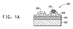
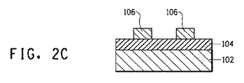
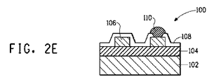
図1は、金属コア基板を使用する電子デバイス100の構造を概略的に示す。参照符号102は板状金属ベースを示し、104は絶縁層を示し、106は電子回路を示す。図1に示されるように、絶縁層104が板状金属ベース上に設けられ、電子回路がこの絶縁層上に形成される。さらに、電子回路106は、はんだ110を有する電子部品、実装部品またはモジュール部品等の末端部分に接続されたそれらの部分を除いて、耐久性を考慮して保護膜108によって覆われる。絶縁層、電子回路等の厚さまたは他の条件に特定の制限条件はない。これらの条件は、金属コア基板を使用する電子デバイスにおいて通常に使用される条件の範囲内でありうる。
FIG. 1 schematically illustrates the structure of an
板状金属ベース102は、Cu、Al、Fe、ステンレス鋼、NiまたはFeNiなどの様々な金属または合金から製造された板状ベースからなってもよい。また、無機粒子(SiC、Al2O3、AlN、BN、WCまたはSiNなど)、無機充填剤、セラミック粒子またはセラミック充填剤などの様々な材料が、電子デバイスの特性を改良するために、これらの金属または合金中に含有されてもよい。
The
また、板状ベースは、複数の材料からなる積層体の形態であってもよい。 Further, the plate-like base may be in the form of a laminate made of a plurality of materials.
本発明の金属コア基板のための上述の絶縁ペーストが絶縁層104において用いられる。
The insulating paste described above for the metal core substrate of the present invention is used in the insulating
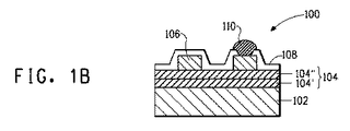
本発明の電子デバイスにおいて、絶縁層104は、(図1Aに示された単一層のような)単一層からなってもよく、または2つ以上のタイプの絶縁ペーストを含む多数の層からなってもよい(2つの層の例が図1Bに示される)。絶縁層が多数の層からなる場合、本発明の金属コア基板のための絶縁ペーストは、少なくとも最上層104”(電子回路が上に形成される層)において使用されることが必要とされる。このように、本発明において、絶縁層が多数の層からなる場合、最上層以外の層104’(電子回路が上に形成される層)は、本発明の金属コア基板のための絶縁ペーストまたは別の絶縁ペーストを使用することができる。
In the electronic device of the present invention, the insulating
導体ペーストが電子回路106において用いられる。金属コア基板の絶縁層上に回路を形成する時に使用される場合、導体ペーストに特定の制限条件はない。例えば、導体ペーストは、必要に応じて導電性金属およびビヒクル、ならびにガラス粉末、無機酸化物等を含有する。ガラス粉末、無機酸化物等は、導電性金属の100重量%に対して好ましくは10重量%以下、より好ましくは0〜5重量%、さらにより好ましくは0〜3重量%において含有される。
Conductive paste is used in the
導電性金属は好ましくは金、銀、銅、パラジウム、白金、ニッケル、アルミニウムまたはそれらの合金である。導電性金属の平均粒子径は好ましくは8μm以下である。 The conductive metal is preferably gold, silver, copper, palladium, platinum, nickel, aluminum or an alloy thereof. The average particle diameter of the conductive metal is preferably 8 μm or less.
ガラス粉末の例には、ケイ酸鉛ガラス、ホウケイ酸鉛ガラスおよびビスマス−亜鉛−シリカ−ホウ素ガラスなどがある。さらに、無機酸化物の例には、Al2O3、SiO2、TiO2、MnO、MgO、ZrO2、CaO、BaOおよびCo2O3などがある。ビヒクルの例には、バインダー樹脂(例えばエチルセルロース樹脂、アクリル樹脂、ロジン改質樹脂またはポリビニルブチラール樹脂)と有機溶剤(例えばブチルカルビトールアセテート(BCA)、テルピネオール、エステルアルコール、BCまたはTPO)との有機混合物がある。 Examples of glass powders include lead silicate glass, lead borosilicate glass and bismuth-zinc-silica-boron glass. Further, examples of the inorganic oxide include Al 2 O 3 , SiO 2 , TiO 2 , MnO, MgO, ZrO 2 , CaO, BaO and Co 2 O 3 . Examples of vehicles include organics of binder resins (eg ethyl cellulose resin, acrylic resin, rosin modified resin or polyvinyl butyral resin) and organic solvents (eg butyl carbitol acetate (BCA), terpineol, ester alcohol, BC or TPO). There is a mixture.
導体ペーストを適切に製造するために、例えば、上の成分の各々をミキサで混合し、3本ロールミル等で分散させた。 In order to produce a conductor paste appropriately, for example, each of the above components was mixed with a mixer and dispersed with a three-roll mill or the like.
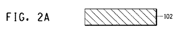
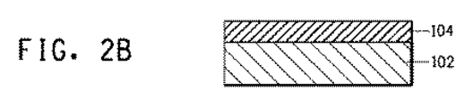
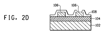
本発明の電子デバイスは、例えば、図2に示されたような方法を用いて製造されうる。図2は、絶縁層の単一層を含有する電子デバイスの製造方法を示す実施例である。最初に、板状金属ベース102が作製される(図2A)。次に、本発明の金属コア基板のための絶縁ペーストを、例えばスクリーン印刷によってこの板状金属ベース上に印刷し、その後、焼成して絶縁層104を得る(図2B)。複数の絶縁層を形成する場合、この工程は、所望の数の層のために繰り返される。次に、電子回路106を形成するための導体ペーストを所望のパターンでスクリーン印刷等によって絶縁層上に印刷し、その後、焼成する(図2C)。次に、保護膜108をスクリーン印刷等によって所望のパターンで印刷する(図2D)。この場合、電子部品、実装部品またはモジュール部品等の末端部分にはんだ110で接続された部分を除いて全ての成分を覆うように保護膜を印刷する。ガラスまたはガラスおよびセラミックからなる保護膜の場合、それは、導体ペーストの焼成温度以下の温度で焼成される。保護膜のためにエポキシ樹脂などの有機材料を使用する場合、保護膜は、100〜200℃の範囲内の温度において熱硬化することによって形成される。次いで、はんだペーストを、各部品の末端位置に接続された部分に印刷し、予め決められた位置にそれらの部品を取り付けた後、はんだリフロー炉内ではんだ付けすることによってそれらを取り付ける(図2E)。
The electronic device of the present invention can be manufactured using, for example, a method as shown in FIG. FIG. 2 is an example illustrating a method for manufacturing an electronic device containing a single layer of an insulating layer. First, the plate-shaped
本発明において、絶縁ペーストが金属コア基板のために用いられる(あるいは、絶縁層が多数の層からなる場合には少なくとも最上層において用いられる)。これは、絶縁層から導電膜中へのガラスの拡散を防ぐことにつながり、以前は、生じた場合には、それは650℃以下の焼成温度において金属コア基板上に絶縁層および電子回路を形成する時に問題を生じた。結果として、導体とはんだとの間の接触抵抗を低下させることができ、はんだ付け適性を有する絶縁層上に高信頼性の電子回路を形成することができ、電子回路の正確な配置を行なうことができる。 In the present invention, an insulating paste is used for the metal core substrate (or, in the case where the insulating layer is composed of a plurality of layers, it is used in at least the uppermost layer). This leads to preventing the diffusion of the glass from the insulating layer into the conductive film, which previously formed the insulating layer and electronic circuit on the metal core substrate at a firing temperature of 650 ° C. or lower, if it occurred. Sometimes there was a problem. As a result, the contact resistance between the conductor and the solder can be reduced, a highly reliable electronic circuit can be formed on the insulating layer having solderability, and the electronic circuit is accurately arranged. Can do.
以下、その実施例によって本発明の詳細な説明を記載するが、これらの実施例は、例示目的であることを意図するにすぎず、本発明を限定するものではない。 Hereinafter, the present invention will be described in detail by way of examples, but these examples are only intended for illustrative purposes and are not intended to limit the present invention.
(A)金属コア基板のための絶縁ペーストおよび導体ペーストの調製
金属コア基板のための絶縁ペーストおよび導体ペーストを表1に示された調合量によって調製した。
(A) Preparation of Insulating Paste and Conductive Paste for Metal Core Substrate Insulating paste and conductive paste for metal core substrate were prepared according to the blending amounts shown in Table 1.

表に示された材料の各々は以下に記載された通りである。 Each of the materials shown in the table is as described below.
ガラスA:ガラス網目組成物としてAl2O3を有するガラス(Bi2O3−SiO2−B2O3ベースのガラス)を溶融および急冷し、その後、TiO2セラミック充填剤をそれに添加し、その後、混合した(Al2O3:TiO2=4.8:14.4)。 Glass A: Glass with Al 2 O 3 as glass network composition (Bi 2 O 3 —SiO 2 —B 2 O 3 based glass) is melted and quenched, then TiO 2 ceramic filler is added to it, then, mixed (Al 2 O 3: TiO 2 = 4.8: 14.4).
ガラスB:ガラス網目組成物としてAl2O3を有するガラス(Bi2O3−SiO2−B2O3ベースのガラス)を溶融および急冷し、その後、TiOセラミック充填剤をそれに添加し、その後、混合した(Al2O3:TiO2=3.0:11.3)。 Glass B: Glass with Al 2 O 3 as glass network composition (Bi 2 O 3 —SiO 2 —B 2 O 3 based glass) is melted and quenched, then TiO ceramic filler is added to it, then (Al 2 O 3 : TiO 2 = 3.0: 11.3).
ガラスC:ガラス網目組成物としてAl2O3およびTiO2を有する(Al2O3:TiO2=2.0:0.1)ガラス(Bi2O3−SiO2−B2O3ベースのガラス)を溶融および急冷した。 Glass C: based on glass (Bi 2 O 3 —SiO 2 —B 2 O 3 ) with Al 2 O 3 and TiO 2 as glass network composition (Al 2 O 3 : TiO 2 = 2.0: 0.1) Glass) was melted and quenched.
ガラスD:ガラス網目組成物としてAl2O3を有する(Al2O3=0.5)ガラス(Bi2O3−SiO2−B2O3ベースのガラス)を溶融および急冷した。 Glass D: (Al 2 O 3 = 0.5) glass (Bi 2 O 3 —SiO 2 —B 2 O 3 based glass) having Al 2 O 3 as a glass network composition was melted and quenched.
Al2O3:平均粒子径:0.4〜0.6μm
TiO2:平均粒子径:0.4〜0.6μm
銀粉末:1.4〜1.6μmの平均粒子径を有する球状粉末
樹脂溶液:テルピネオール中に溶解されたエチルセルロース樹脂(エチルセルロース樹脂:テルピネオール=10:90(wt/wt))
希釈溶剤:テルピネオールまたはブチルカルビトールアセテート
各成分を各ペーストの調合に従って容器内で秤量し、その後、ミキサで混合し、三本ロールミルで分散させた。
Al 2 O 3 : Average particle diameter: 0.4 to 0.6 μm
TiO 2 : Average particle diameter: 0.4 to 0.6 μm
Silver powder: spherical powder having an average particle size of 1.4 to 1.6 μm Resin solution: ethyl cellulose resin dissolved in terpineol (ethyl cellulose resin: terpineol = 10: 90 (wt / wt))
Diluting solvent: terpineol or butyl carbitol acetate Each component was weighed in a container according to the formulation of each paste, then mixed in a mixer and dispersed in a three-roll mill.
(B)金属コア基板上の絶縁層および回路の形成
絶縁層および銀導体回路を金属コア基板上に形成した。回路基板を形成するための方法は以下に記載された通りである。
(B) Formation of insulating layer and circuit on metal core substrate An insulating layer and a silver conductor circuit were formed on the metal core substrate. The method for forming the circuit board is as described below.
形成方法1(実施例1、2、3、4、5および比較例1および2)
第1の絶縁ペースト(下層)を、焼成後の厚さ20μmにスクリーン印刷することによってステンレス鋼(SUS430)基板(板状金属ベース)上に印刷した。次に、10分間550℃に維持する合計30分のプロファイルでベルト炉内で基板を焼成して、絶縁層1を得た。次いで、第2の絶縁ペースト(上層)を、第1の絶縁ペーストと同じ条件下でスクリーン印刷することによって絶縁層1上に印刷し、その後、焼成した。結果として、絶縁層2が形成された。最後に、銀ペーストを第2の絶縁層上に、焼成後の厚さ15μmに印刷して、絶縁ペーストと同じ条件下で焼成することによって銀導体回路を形成した。
Formation Method 1 (Examples 1, 2, 3, 4, 5 and Comparative Examples 1 and 2)
The first insulating paste (lower layer) was printed on a stainless steel (SUS430) substrate (plate metal base) by screen printing to a thickness of 20 μm after firing. Next, the board | substrate was baked in the belt furnace with the profile for a total of 30 minutes maintained at 550 degreeC for 10 minutes, and the insulating layer 1 was obtained. Next, the second insulating paste (upper layer) was printed on the insulating layer 1 by screen printing under the same conditions as the first insulating paste, and then fired. As a result, the insulating layer 2 was formed. Finally, a silver paste was printed on the second insulating layer to a thickness of 15 μm after firing, and fired under the same conditions as the insulating paste to form a silver conductor circuit.
形成方法2(実施例6、7および比較例3および4)
焼成後の厚さ20μmにスクリーン印刷することによって絶縁ペーストをステンレス鋼(SUS430)基板(板状金属ベース)上に印刷した。10分間550℃に維持する合計30分のプロファイルでベルト炉内で基板を焼成した。次に、銀ペーストを焼成後の厚さ15μmに絶縁層上に印刷し、その後、絶縁ペーストと同じ条件下で焼成して銀導体回路を形成した。
Formation method 2 (Examples 6 and 7 and Comparative Examples 3 and 4)
The insulating paste was printed on a stainless steel (SUS430) substrate (plate metal base) by screen printing to a thickness of 20 μm after firing. The substrate was baked in a belt furnace with a total 30 minute profile maintained at 550 ° C. for 10 minutes. Next, a silver paste was printed on the insulating layer to a thickness of 15 μm after firing, and then fired under the same conditions as the insulating paste to form a silver conductor circuit.
(C)評価
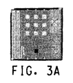
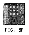
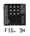
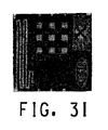
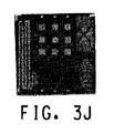
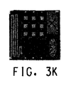
各実施例および比較例の回路基板を、(i)銀導体回路上のはんだ付け適性、(ii)銀導体回路の接着強さ、および(iii)銀導体回路パターンの位置精度について評価した。図3に示された写真のパターンに形成された回路に基づいて各評価を行なった。
(C) Evaluation Regarding the circuit boards of the examples and comparative examples, (i) solderability on the silver conductor circuit, (ii) adhesive strength of the silver conductor circuit, and (iii) positional accuracy of the silver conductor circuit pattern. evaluated. Each evaluation was performed based on the circuit formed in the pattern of the photograph shown in FIG.
(i)銀導体のはんだ付け適性
実施例の各々において作製された絶縁層および銀導体回路を有する金属コア基板は、95.75/3.5/0.75の比で、Sn、AgおよびCuからなる、鉛を含有しないはんだで、240℃において10秒間はんだ付けされた。次いで、導体上のはんだ付け適性を観察した。それらの結果を表2に示す。さらに、評価の基準は以下の通りである。
(I) Solderability of silver conductor The metal core substrate having an insulating layer and a silver conductor circuit produced in each of the examples was Sn, Ag and Cu at a ratio of 95.75 / 3.5 / 0.75. Soldered at 240 ° C. for 10 seconds with lead-free solder. Next, the solderability on the conductor was observed. The results are shown in Table 2. Furthermore, the evaluation criteria are as follows.
評価の基準:
可:銀導体表面の2mm2のパターンに付着したはんだ95%以上
ぎりぎり可:銀導体表面の2mm2のパターンに付着したはんだ80%〜95%未満
不可:銀導体表面の2mm2のパターンに付着したはんだ80%未満
Evaluation criteria:
Yes: silver conductor surface of 2 mm 2 of the solder 95% adhered to the pattern barely soluble: silver conductor 80 percent solder adhered to the pattern of 2 mm 2 of the surface to 95% less than Call: adhering to a pattern of 2 mm 2 of the silver conductor surface Solder less than 80%
(ii)銀導体接着強さ
95.75/3.5/0.75の比で、Sn、AgおよびCuからなる、鉛を含有しないはんだを用いて、スズめっき銅線を2mm2の銀導体パターンに取り付け、その後、引張試験機で基板に垂直な銅線の剥離強度を測定した。それらの結果を表2に示す。
(Ii) Silver conductor adhesive strength Using a lead-free solder composed of Sn, Ag and Cu at a ratio of 95.75 / 3.5 / 0.75, a tin-plated copper wire is a 2 mm 2 silver conductor. After attaching to the pattern, the peel strength of the copper wire perpendicular to the substrate was measured with a tensile tester. The results are shown in Table 2.
(iii)銀導体パターンの位置精度
予め決められた位置からの移動量が、絶縁層上に形成された0.5mm(幅)×100mm(全長)の大きさの銀導体回路パターン(図3のページの向かって左側のパターン)と、微細銀導体回路パターン(図3のページの向かって右上のパターン)とについて観察された。位置変化が生じていない場合は可と評価され、位置変化が生じた場合には不可と評価された。それらの結果を表2に示す。
(Iii) Positional accuracy of silver conductor pattern A silver conductor circuit pattern (0.5 mm (width) x 100 mm (full length)) formed on the insulating layer is moved from a predetermined position (FIG. 3). The pattern on the left side of the page) and the fine silver conductor circuit pattern (the pattern on the upper right side of the page in FIG. 3) were observed. When the position change did not occur, it was evaluated as acceptable, and when the position change occurred, it was evaluated as impossible. The results are shown in Table 2.
図3の写真から明らかであるように、本発明の金属コア基板のための絶縁ペーストを用いる実施例1〜7において、回路パターンの位置変化はなかった(写真の左側および右上隅)。他方、比較例1〜4の回路パターンにおいて位置変化が生じた。 As apparent from the photograph of FIG. 3, in Examples 1 to 7 using the insulating paste for the metal core substrate of the present invention, there was no change in the position of the circuit pattern (left and upper right corners of the photograph). On the other hand, position changes occurred in the circuit patterns of Comparative Examples 1 to 4.
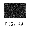
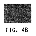
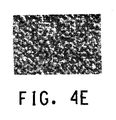
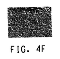
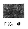
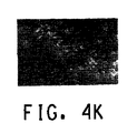
(D)実施例1〜7および比較例1〜4の回路基板の電子顕微鏡による観察の結果
図4は、図3の中央に形成された矩形パターン(銀導体)の表面の電子顕微鏡写真を示す。実施例1〜7において、絶縁層から導電膜へのガラスの拡散は銀導体の表面上で妨げられる。他方、比較例1〜4において、ガラス成分が絶縁層から銀導体回路の表面上へと拡散したのが図4から明らかに観察された。
(D) Results of observation of circuit boards of Examples 1 to 7 and Comparative Examples 1 to 4 with an electron microscope FIG. 4 shows electron micrographs of the surface of a rectangular pattern (silver conductor) formed in the center of FIG. . In Examples 1-7, the diffusion of the glass from the insulating layer to the conductive film is hindered on the surface of the silver conductor. On the other hand, in Comparative Examples 1 to 4, it was clearly observed from FIG. 4 that the glass component diffused from the insulating layer onto the surface of the silver conductor circuit.
これらの実験結果から明らかであるように、本発明の金属コア基板のための絶縁ペーストの使用は、導体とはんだとの間の接触抵抗を低くしたまま銀導体回路のはんだ付け適性を有しかつ銀導体回路の位置変化がない、絶縁層上に高信頼性の回路を形成することを可能にする。 As is clear from these experimental results, the use of the insulating paste for the metal core substrate of the present invention has the solderability of the silver conductor circuit while keeping the contact resistance between the conductor and the solder low, and It is possible to form a highly reliable circuit on the insulating layer without changing the position of the silver conductor circuit.
Claims (9)
を含む、金属コア基板のための絶縁ペーストであって、
アルミナ(Al2O3)およびチタニア(TiO2)の一方または両方がガラス拡散抑制剤として前記ペースト中に含有され、前記ガラス拡散抑制剤の含有量が、前記ペースト中の無機成分の含有量に基づいて12%〜50重量%である、金属コア基板のための絶縁ペースト。 An insulating paste for a metal core substrate comprising (a) glass powder and (b) an organic solvent,
One or both of alumina (Al 2 O 3 ) and titania (TiO 2 ) are contained in the paste as a glass diffusion inhibitor, and the content of the glass diffusion inhibitor is the content of the inorganic component in the paste. Insulating paste for metal core substrates, which is 12% to 50% by weight.
前記板状金属ベース上に形成された1つまたは2つ以上の絶縁層と、
前記絶縁層上に形成された電子回路と
を含む電子デバイスであって、
少なくとも前記電子回路と接触している絶縁層が、ガラス拡散抑制剤としてアルミナ(Al2O3)およびチタニア(TiO2)の一方または両方を含有し、
前記ガラス拡散抑制剤の含有量が、前記絶縁層中の無機成分の含有量に基づいて12〜50重量%である、電子デバイス。 A plate-like metal base;
One or more insulating layers formed on the plate-like metal base;
An electronic device comprising an electronic circuit formed on the insulating layer,
At least the insulating layer in contact with the electronic circuit contains one or both of alumina (Al 2 O 3 ) and titania (TiO 2 ) as a glass diffusion inhibitor,
The electronic device whose content of the said glass diffusion inhibitor is 12 to 50 weight% based on content of the inorganic component in the said insulating layer.
Applications Claiming Priority (2)
| Application Number | Priority Date | Filing Date | Title |
|---|---|---|---|
| US11/820,986 US20080318061A1 (en) | 2007-06-20 | 2007-06-20 | Insulation paste for a metal core substrate and electronic device |
| PCT/US2008/067465 WO2008157675A1 (en) | 2007-06-20 | 2008-06-19 | Insulation paste for a metal core substrate and electronic device |
Publications (2)
| Publication Number | Publication Date |
|---|---|
| JP2010531044A true JP2010531044A (en) | 2010-09-16 |
| JP2010531044A5 JP2010531044A5 (en) | 2011-08-11 |
Family
ID=39789918
Family Applications (1)
| Application Number | Title | Priority Date | Filing Date |
|---|---|---|---|
| JP2010513404A Withdrawn JP2010531044A (en) | 2007-06-20 | 2008-06-19 | Insulating paste for metal core substrates and electronic devices |
Country Status (7)
| Country | Link |
|---|---|
| US (2) | US20080318061A1 (en) |
| EP (1) | EP2155618A1 (en) |
| JP (1) | JP2010531044A (en) |
| KR (1) | KR20100021663A (en) |
| CN (1) | CN101679107A (en) |
| TW (1) | TW200914391A (en) |
| WO (1) | WO2008157675A1 (en) |
Cited By (2)
| Publication number | Priority date | Publication date | Assignee | Title |
|---|---|---|---|---|
| JP2015517226A (en) * | 2012-05-04 | 2015-06-18 | アー.ベー.ミクロエレクトロニクゲゼルシャフト ミト ベシュレンクテル ハフツング | Circuit board, in particular circuit board for a power module comprising a conductive substrate |
| JP2019016740A (en) * | 2017-07-10 | 2019-01-31 | 新光電気工業株式会社 | Lead frame, semiconductor device, and method of manufacturing lead frame |
Families Citing this family (6)
| Publication number | Priority date | Publication date | Assignee | Title |
|---|---|---|---|---|
| WO2009128527A1 (en) * | 2008-04-18 | 2009-10-22 | 日本電気硝子株式会社 | Glass composition for dye-sensitized solar cell and material for dye-sensitized solar cell |
| EP2299536A4 (en) * | 2008-06-17 | 2011-12-21 | Nippon Electric Glass Co | Substrate for solar cell and oxide semiconductor electrode for dye-sensitized solar cell |
| WO2010026952A1 (en) * | 2008-09-04 | 2010-03-11 | 日本電気硝子株式会社 | Glass composition for electrode formation and electrode formation material |
| JP5532512B2 (en) * | 2009-02-24 | 2014-06-25 | 日本電気硝子株式会社 | Electrode forming glass composition and electrode forming material |
| JP2011044426A (en) | 2009-07-24 | 2011-03-03 | Nippon Electric Glass Co Ltd | Glass substrate with conductive film for solar cell |
| JP6787286B2 (en) * | 2017-09-20 | 2020-11-18 | 株式会社村田製作所 | Manufacturing method of inductor parts |
Family Cites Families (10)
| Publication number | Priority date | Publication date | Assignee | Title |
|---|---|---|---|---|
| GB1171784A (en) * | 1966-11-17 | 1969-11-26 | English Electric Co Ltd | Improvements in or relating to Processes for Forming an Insulating Coating on a Metal, and to Coated Metals. |
| CS219732B1 (en) * | 1981-01-21 | 1983-03-25 | Radomir Kuzel | Method of making the isolation coatings on the steel products |
| NL8100816A (en) * | 1981-02-19 | 1982-09-16 | Philips Nv | WIRE INJURED RESISTANCE. |
| US4556598A (en) * | 1983-06-16 | 1985-12-03 | Cts Corporation | Porcelain tape for producing porcelainized metal substrates |
| JPS63170994A (en) * | 1986-05-30 | 1988-07-14 | 古河電気工業株式会社 | Multilayer printed interconnection board and manufacture of the same |
| US5002818A (en) * | 1989-09-05 | 1991-03-26 | Hughes Aircraft Company | Reworkable epoxy die-attach adhesive |
| US6233817B1 (en) * | 1999-01-17 | 2001-05-22 | Delphi Technologies, Inc. | Method of forming thick-film hybrid circuit on a metal circuit board |
| WO2001044143A1 (en) * | 1999-12-16 | 2001-06-21 | Tokuyama Corporation | Joint body of glass-ceramic and aluminum nitride sintered compact and method for producing the same |
| JP2004175645A (en) * | 2002-11-29 | 2004-06-24 | Asahi Glass Co Ltd | Glass frit mixture, method of manufacturing electronic circuit board and electronic circuit board |
| JP4407199B2 (en) * | 2003-08-13 | 2010-02-03 | 旭硝子株式会社 | Crystallized lead-free glass, glass ceramic composition, green sheet and electronic circuit board |
-
2007
- 2007-06-20 US US11/820,986 patent/US20080318061A1/en not_active Abandoned
-
2008
- 2008-06-19 JP JP2010513404A patent/JP2010531044A/en not_active Withdrawn
- 2008-06-19 KR KR1020107001225A patent/KR20100021663A/en not_active Application Discontinuation
- 2008-06-19 EP EP08771449A patent/EP2155618A1/en not_active Withdrawn
- 2008-06-19 WO PCT/US2008/067465 patent/WO2008157675A1/en active Application Filing
- 2008-06-19 CN CN200880018049.2A patent/CN101679107A/en active Pending
- 2008-06-20 TW TW097123260A patent/TW200914391A/en unknown
-
2010
- 2010-04-27 US US12/768,202 patent/US20100200283A1/en not_active Abandoned
Cited By (5)
| Publication number | Priority date | Publication date | Assignee | Title |
|---|---|---|---|---|
| JP2015517226A (en) * | 2012-05-04 | 2015-06-18 | アー.ベー.ミクロエレクトロニクゲゼルシャフト ミト ベシュレンクテル ハフツング | Circuit board, in particular circuit board for a power module comprising a conductive substrate |
| KR101603861B1 (en) | 2012-05-04 | 2016-03-16 | 아베 미크로엘렉트로닉 게젤샤프트 미트 베슈렝크터 하프퉁 | Circuit board, particularly for a power-electronic module, comprising an electrically-conductive substrate |
| US9648736B2 (en) | 2012-05-04 | 2017-05-09 | A.B. Mikroelektronik Gesellschaft Mit Beschraenkter Haftung | Circuit board, particularly for a power-electronic module, comprising an electrically-conductive substrate |
| US10091874B2 (en) | 2012-05-04 | 2018-10-02 | Ab Mikroelektronik Gesellschaft Mit Beschraenkter Haftung | Circuit board, particulary for a power-electronic module, comprising an electrically-conductive substrate |
| JP2019016740A (en) * | 2017-07-10 | 2019-01-31 | 新光電気工業株式会社 | Lead frame, semiconductor device, and method of manufacturing lead frame |
Also Published As
| Publication number | Publication date |
|---|---|
| WO2008157675A1 (en) | 2008-12-24 |
| US20100200283A1 (en) | 2010-08-12 |
| US20080318061A1 (en) | 2008-12-25 |
| TW200914391A (en) | 2009-04-01 |
| EP2155618A1 (en) | 2010-02-24 |
| CN101679107A (en) | 2010-03-24 |
| KR20100021663A (en) | 2010-02-25 |
Similar Documents
| Publication | Publication Date | Title |
|---|---|---|
| JP5303552B2 (en) | Conductive paste for ceramic substrate and electric circuit | |
| US7504349B2 (en) | Lead-free and cadmium-free conductive copper thick film pastes | |
| JP5180443B2 (en) | Thick film conductor paste composition for LTCC tape in microwave applications | |
| JP2010531044A (en) | Insulating paste for metal core substrates and electronic devices | |
| JP3528037B2 (en) | Manufacturing method of glass ceramic substrate | |
| KR101799128B1 (en) | Electronic component and method for producing same | |
| JP2012022841A (en) | Conductive paste | |
| JP4432604B2 (en) | Conductive paste | |
| US20050106369A1 (en) | Thick film conductor case compositions for LTCC tape | |
| US7731812B2 (en) | Thick film conductor case compositions for LTCC tape | |
| JP2006074008A (en) | High thermal cycle conductor system | |
| CN112673435B (en) | Conductive thick film pastes for silicon nitride and other substrates | |
| US7740725B2 (en) | Thick film conductor paste composition for LTCC tape in microwave applications | |
| JP2004055558A (en) | Copper paste and wiring board using the same | |
| JP4646362B2 (en) | Conductor composition and wiring board using the same | |
| JP3652184B2 (en) | Conductive paste, glass-ceramic wiring board and manufacturing method thereof |
Legal Events
| Date | Code | Title | Description |
|---|---|---|---|
| A521 | Request for written amendment filed |
Free format text: JAPANESE INTERMEDIATE CODE: A523 Effective date: 20110620 |
|
| A621 | Written request for application examination |
Free format text: JAPANESE INTERMEDIATE CODE: A621 Effective date: 20110620 |
|
| A761 | Written withdrawal of application |
Free format text: JAPANESE INTERMEDIATE CODE: A761 Effective date: 20130408 |