JP2010530726A - Charge pump circuit and operation method thereof - Google Patents
Charge pump circuit and operation method thereof Download PDFInfo
- Publication number
- JP2010530726A JP2010530726A JP2009542239A JP2009542239A JP2010530726A JP 2010530726 A JP2010530726 A JP 2010530726A JP 2009542239 A JP2009542239 A JP 2009542239A JP 2009542239 A JP2009542239 A JP 2009542239A JP 2010530726 A JP2010530726 A JP 2010530726A
- Authority
- JP
- Japan
- Prior art keywords
- terminal
- state
- output
- capacitor
- mode
- Prior art date
- Legal status (The legal status is an assumption and is not a legal conclusion. Google has not performed a legal analysis and makes no representation as to the accuracy of the status listed.)
- Pending
Links
Images


Classifications
-
- H—ELECTRICITY
- H02—GENERATION; CONVERSION OR DISTRIBUTION OF ELECTRIC POWER
- H02M—APPARATUS FOR CONVERSION BETWEEN AC AND AC, BETWEEN AC AND DC, OR BETWEEN DC AND DC, AND FOR USE WITH MAINS OR SIMILAR POWER SUPPLY SYSTEMS; CONVERSION OF DC OR AC INPUT POWER INTO SURGE OUTPUT POWER; CONTROL OR REGULATION THEREOF
- H02M3/00—Conversion of dc power input into dc power output
- H02M3/02—Conversion of dc power input into dc power output without intermediate conversion into ac
- H02M3/04—Conversion of dc power input into dc power output without intermediate conversion into ac by static converters
- H02M3/06—Conversion of dc power input into dc power output without intermediate conversion into ac by static converters using resistors or capacitors, e.g. potential divider
- H02M3/07—Conversion of dc power input into dc power output without intermediate conversion into ac by static converters using resistors or capacitors, e.g. potential divider using capacitors charged and discharged alternately by semiconductor devices with control electrode, e.g. charge pumps
-
- H—ELECTRICITY
- H02—GENERATION; CONVERSION OR DISTRIBUTION OF ELECTRIC POWER
- H02M—APPARATUS FOR CONVERSION BETWEEN AC AND AC, BETWEEN AC AND DC, OR BETWEEN DC AND DC, AND FOR USE WITH MAINS OR SIMILAR POWER SUPPLY SYSTEMS; CONVERSION OF DC OR AC INPUT POWER INTO SURGE OUTPUT POWER; CONTROL OR REGULATION THEREOF
- H02M1/00—Details of apparatus for conversion
- H02M1/0083—Converters characterised by their input or output configuration
- H02M1/009—Converters characterised by their input or output configuration having two or more independently controlled outputs
-
- H—ELECTRICITY
- H02—GENERATION; CONVERSION OR DISTRIBUTION OF ELECTRIC POWER
- H02M—APPARATUS FOR CONVERSION BETWEEN AC AND AC, BETWEEN AC AND DC, OR BETWEEN DC AND DC, AND FOR USE WITH MAINS OR SIMILAR POWER SUPPLY SYSTEMS; CONVERSION OF DC OR AC INPUT POWER INTO SURGE OUTPUT POWER; CONTROL OR REGULATION THEREOF
- H02M3/00—Conversion of dc power input into dc power output
- H02M3/02—Conversion of dc power input into dc power output without intermediate conversion into ac
- H02M3/04—Conversion of dc power input into dc power output without intermediate conversion into ac by static converters
- H02M3/06—Conversion of dc power input into dc power output without intermediate conversion into ac by static converters using resistors or capacitors, e.g. potential divider
- H02M3/07—Conversion of dc power input into dc power output without intermediate conversion into ac by static converters using resistors or capacitors, e.g. potential divider using capacitors charged and discharged alternately by semiconductor devices with control electrode, e.g. charge pumps
- H02M3/071—Conversion of dc power input into dc power output without intermediate conversion into ac by static converters using resistors or capacitors, e.g. potential divider using capacitors charged and discharged alternately by semiconductor devices with control electrode, e.g. charge pumps adapted to generate a negative voltage output from a positive voltage source
-
- H—ELECTRICITY
- H02—GENERATION; CONVERSION OR DISTRIBUTION OF ELECTRIC POWER
- H02M—APPARATUS FOR CONVERSION BETWEEN AC AND AC, BETWEEN AC AND DC, OR BETWEEN DC AND DC, AND FOR USE WITH MAINS OR SIMILAR POWER SUPPLY SYSTEMS; CONVERSION OF DC OR AC INPUT POWER INTO SURGE OUTPUT POWER; CONTROL OR REGULATION THEREOF
- H02M3/00—Conversion of dc power input into dc power output
- H02M3/02—Conversion of dc power input into dc power output without intermediate conversion into ac
- H02M3/04—Conversion of dc power input into dc power output without intermediate conversion into ac by static converters
- H02M3/06—Conversion of dc power input into dc power output without intermediate conversion into ac by static converters using resistors or capacitors, e.g. potential divider
- H02M3/07—Conversion of dc power input into dc power output without intermediate conversion into ac by static converters using resistors or capacitors, e.g. potential divider using capacitors charged and discharged alternately by semiconductor devices with control electrode, e.g. charge pumps
- H02M3/072—Conversion of dc power input into dc power output without intermediate conversion into ac by static converters using resistors or capacitors, e.g. potential divider using capacitors charged and discharged alternately by semiconductor devices with control electrode, e.g. charge pumps adapted to generate an output voltage whose value is lower than the input voltage
Abstract
1つのフライングキャパシタ(cf)を使用して、複数の出力電圧(Vout+,Vout-)を供給するためのデュアルモードチャージポンプ回路(400)、ならびに関連する方法および装置が開示される。前記回路は、多くの異なる状態で動作可能なスイッチ網(410)と、第1モードにおいて、合計して前記入力電圧(+VDD)にほぼ等しい電圧になり、かつ前記共通端子の前記電圧を中心とする正負の出力電圧(Vout+,Vout-)を生成し、第2モードにおいて、それぞれが実質的に前記入力電圧(+VDD)に達する正負の出力電圧を供給するために、前記スイッチを前記状態のシーケンスで作動させるためのコントローラ(420)とを有する。
A dual mode charge pump circuit (400) for supplying a plurality of output voltages (V out + , V out− ) using a single flying capacitor (cf) and related methods and apparatus are disclosed. The circuit includes a switch network (410) operable in a number of different states and, in the first mode, totals a voltage approximately equal to the input voltage (+ V DD ) and is centered on the voltage at the common terminal. To generate positive and negative output voltages (V out + , V out− ), and in the second mode, to supply positive and negative output voltages, each of which substantially reaches the input voltage (+ V DD ). A controller (420) for operating in the sequence of states.
Description
本発明は、チャージポンプ回路、より詳細には、デュアルレール出力を提供するチャージポンプ回路に関する。 The present invention relates to a charge pump circuit, and more particularly to a charge pump circuit that provides a dual rail output.
チャージポンプ回路は、当業界において公知である。このような回路は、エネルギ蓄積装置としてキャパシタを使用し、入力源よりも昇圧または降圧された電力源を供給可能なDC−DCコンバータの一種である。チャージポンプ回路は、高効率(時に90〜95%もの高効率)が可能である。 Charge pump circuits are well known in the art. Such a circuit is a type of DC-DC converter that uses a capacitor as an energy storage device and can supply a power source that is stepped up or stepped down from an input source. The charge pump circuit can be highly efficient (sometimes as high as 90-95%).
チャージポンプは、キャパシタと電圧源およびキャパシタ間の接続を制御する何らかの形の切替装置を使用して、通常、入力電圧値とは異なる電圧を得ている。チャージポンプは、「リザーバキャパシタ」と以降呼ぶ1つ以上の出力キャパシタに電荷を転送するための、「フライングキャパシタ」として一般に知られているキャパシタを備える。このようなチャージポンプは、シングルレールの入力電圧VDDから2極性の供給電圧を生成するために使用されうる。公知のデュアルレールチャージポンプの欠点として、例えば、チャージポンプが、入力電圧(VDD)の2倍の値の出力電圧、すなわち、共通端子に対して一方のレールが電圧VDDを、もう一方のレールが−VDDを生成しうるという点が挙げられる。このようなチャージポンプが、例えば、増幅器回路の電力供給±VDDよりも最大振幅の極めて小さい信号を増幅するパワー回路に使用される場合に、この点が極めて非効率となりうる。このような場合、出力電力(このため入力電力)の大部分は、信号の駆動ではなく熱の発生に浪費される。しかし、当然、必要な場合にこのフル出力レンジも選択できることが時には有利となる。 Charge pumps typically obtain a voltage different from the input voltage value using some form of switching device that controls the connection between the capacitor and the voltage source and the capacitor. The charge pump includes a capacitor commonly known as a “flying capacitor” for transferring charge to one or more output capacitors, hereinafter referred to as “reservoir capacitors”. Such a charge pump can be used to generate a bipolar supply voltage from a single rail input voltage VDD. A disadvantage of the known dual rail charge pump is, for example, that the charge pump has an output voltage that is twice the input voltage (VDD), that is, one rail is at the voltage VDD with respect to the common terminal and the other rail is at the other. -VDD can be generated. This can be very inefficient when such a charge pump is used, for example, in a power circuit that amplifies a signal with a very small maximum amplitude than the power supply ± VDD of the amplifier circuit. In such a case, most of the output power (and hence input power) is wasted in generating heat rather than driving the signal. Of course, however, it is sometimes advantageous to be able to select this full output range if necessary.
本発明の目的は、上述の欠点に対処することにある。 The object of the present invention is to address the above-mentioned drawbacks.
本発明の第1の態様においては、入力端子および共通端子の両端に入力される1つの入力供給から分割レール電圧供給を生成する方法であって、前記分割レール供給は、個々の第1負荷および第2負荷と、個々の第1リザーバキャパシタおよび第2リザーバキャパシタとを介して前記共通端子に接続された第1出力端子および第2出力端子に出力され、前記方法は、
状態シーケンスにおいて前記異なる端子間にフライングキャパシタを接続し、前記入力供給から前記リザーバキャパシタに、直接または前記フライングキャパシタを介して電荷のパケットを繰り返し転送し、これにより、選択された動作モードに応じて、合計して前記入力電圧にほぼ等しい電圧になり、かつ前記共通端子の前記電圧を中心とする正負の出力電圧か、それぞれが実質的に前記入力供給に達する正負の出力電圧を有する前記分割レール供給を生成するステップを有する方法が提供される。
In a first aspect of the present invention, there is provided a method for generating a split rail voltage supply from one input supply input at both ends of an input terminal and a common terminal, wherein the split rail supply includes individual first loads and Output to a first output terminal and a second output terminal connected to the common terminal via a second load and individual first and second reservoir capacitors, the method comprising:
Connecting a flying capacitor between the different terminals in a state sequence and repeatedly transferring a packet of charge from the input supply to the reservoir capacitor directly or via the flying capacitor, thereby depending on the selected operating mode The divided rails having a positive or negative output voltage centered on the voltage of the common terminal, or a positive or negative output voltage that substantially reaches the input supply. A method is provided that includes generating a feed.
また、入力端子および共通端子の両端に入力される1つの入力供給から分割レール電圧供給を生成する方法であって、前記分割レール供給は、個々の第1負荷および第2負荷と、個々の第1リザーバキャパシタおよび第2リザーバキャパシタとを介して前記共通端子に接続された第1出力端子および第2出力端子に出力され、前記方法は、
1つのフライングキャパシタを使用して、選択された動作モードに応じて、合計して前記入力電圧にほぼ等しい電圧になり、かつ前記共通端子の前記電圧を中心とする正負の出力電圧か、それぞれが実質的に前記入力供給に達する正負の出力電圧を有する前記分割レール供給を生成する方法も開示される。
A method of generating a split rail voltage supply from one input supply input to both ends of an input terminal and a common terminal, wherein the split rail supply includes individual first loads and second loads, and individual first loads. Output to a first output terminal and a second output terminal connected to the common terminal via one reservoir capacitor and a second reservoir capacitor, the method comprising:
Using one flying capacitor, depending on the selected operation mode, the total voltage is approximately equal to the input voltage, and each of the positive and negative output voltages centered on the voltage of the common terminal is A method of generating the split rail supply having positive and negative output voltages that substantially reach the input supply is also disclosed.
前記方法は、第1モードでの動作時に、少なくとも第1状態と第2状態を交互に反復するステップを有し、前記第1状態は、前記入力電圧を前記フライングキャパシタと第1リザーバキャパシタ間で直列に分割するのに有効であり、前記第2状態は、前記フライングキャパシタの分割された前記電圧の一部を前記第2リザーバキャパシタに印加するのに有効であってもよい。前記第1状態は、前記入力端子と前記第1出力端子との間に前記フライングキャパシタを接続することによって得られ、前記第2状態は、前記共通端子と前記第2出力端子との間に前記フライングキャパシタを接続することによって得られてもよい。前記第1モードにおける前記シーケンスは、第3状態の反復を含み、前記第3状態は、前記フライングキャパシタの分割された前記電圧の一部を前記第1リザーバキャパシタに印加するのに有効であってもよい。前記第3状態は、前記第1出力端子と前記共通端子との間に前記フライングキャパシタを接続することによって得られてもよい。 The method includes the step of alternately repeating at least a first state and a second state when operating in a first mode, wherein the first state causes the input voltage to pass between the flying capacitor and the first reservoir capacitor. Effective in dividing in series, the second state may be effective in applying a portion of the divided voltage of the flying capacitor to the second reservoir capacitor. The first state is obtained by connecting the flying capacitor between the input terminal and the first output terminal, and the second state is between the common terminal and the second output terminal. It may be obtained by connecting a flying capacitor. The sequence in the first mode includes repetition of a third state, the third state being effective to apply a portion of the divided voltage of the flying capacitor to the first reservoir capacitor. Also good. The third state may be obtained by connecting the flying capacitor between the first output terminal and the common terminal.
前記方法は、第1モードでの動作時に、第4状態と第5状態を交互に反復するステップを有し、前記第4状態は、前記フライングキャパシタを前記入力電圧まで充電するのに有効であり、前記第5状態は、前記フライングキャパシタ上の電圧を前記第1リザーバキャパシタと第2リザーバキャパシタ間で直列に分割するのに有効であってもよい。前記第4状態は、前記入力端子と前記共通端子との間に前記フライングキャパシタを接続することによって得られ、前記第5状態は、前記第1出力端子と前記第2出力端子との間に前記フライングキャパシタを接続することによって得られてもよい。 The method includes alternately repeating a fourth state and a fifth state when operating in the first mode, and the fourth state is effective for charging the flying capacitor to the input voltage. The fifth state may be effective for dividing the voltage on the flying capacitor in series between the first reservoir capacitor and the second reservoir capacitor. The fourth state can be obtained by connecting the flying capacitor between the input terminal and the common terminal, and the fifth state can be obtained between the first output terminal and the second output terminal. It may be obtained by connecting a flying capacitor.
前記方法は、第2モードでの動作時に、少なくとも第2状態と第6状態を交互に反復するステップを有し、前記第6状態は、前記フライングキャパシタおよび前記第1リザーバキャパシタを実質的に前記入力電圧まで充電するのに有効であり、前記第2状態は、前記フライングキャパシタから前記第2リザーバキャパシタに前記電圧を転送するのに有効であってもよい。前記第2状態は、前記共通端子と前記第2出力端子との間に前記フライングキャパシタを接続することによって得られ、前記第6状態は、前記入力端子を前記第1出力端子に接続し、このノードと前記共通端子との間に前記フライングキャパシタを接続することによって得られてもよい。前記第2モードにおける前記シーケンスは、第7状態の反復を含み、前記第7状態は、いずれのリザーバキャパシタとも独立して、前記フライングキャパシタを充電するのに有効であってもよい。前記第7状態は、前記入力端子と前記共通端子との間に前記フライングキャパシタを接続し、前記入力端子を前記第1出力端子から分離することによって得られてもよい。 The method includes alternately repeating at least a second state and a sixth state when operating in a second mode, wherein the sixth state substantially includes the flying capacitor and the first reservoir capacitor. The second state may be effective for charging up to an input voltage, and the second state may be effective for transferring the voltage from the flying capacitor to the second reservoir capacitor. The second state is obtained by connecting the flying capacitor between the common terminal and the second output terminal, and the sixth state connects the input terminal to the first output terminal. It may be obtained by connecting the flying capacitor between a node and the common terminal. The sequence in the second mode may include a seventh state iteration, and the seventh state may be effective to charge the flying capacitor independently of any reservoir capacitor. The seventh state may be obtained by connecting the flying capacitor between the input terminal and the common terminal and separating the input terminal from the first output terminal.
第2モードの特定の実装における動作時に、前記フライングキャパシタから独立して、前記入力端子と前記第1出力端子間に接続が維持され、これにより、この特定の実装での動作時に、前記第1リザーバキャパシタが前記入力端子と前記共通端子間に常に接続されることが保証されてもよい。 During operation in a particular implementation of the second mode, a connection is maintained between the input terminal and the first output terminal independently of the flying capacitor, so that when operating in this particular implementation, the first It may be ensured that a reservoir capacitor is always connected between the input terminal and the common terminal.
ここに開示した変形例のいずれかにおいて、第2動作モードを実装するために選択信号が使用されてもよい。 In any of the variations disclosed herein, a selection signal may be used to implement the second mode of operation.
前記状態に応じて、前記フライングキャパシタの一方が、前記入力端子、前記第1出力端子または前記共通端子の1つに独立して接続されてもよい。 Depending on the state, one of the flying capacitors may be independently connected to one of the input terminal, the first output terminal or the common terminal.
もう一方のフライングキャパシタ端子が、前記第1出力端子、前記共通端子または前記第2出力端子の1つに独立して接続されてもよい。 The other flying capacitor terminal may be independently connected to one of the first output terminal, the common terminal, or the second output terminal.
任意の状態シーケンスが負荷条件に応じて変更されてもよい。前記状態シーケンスの前記変形例は、前記負荷は非対称的の場合に、前記第2状態を含む前記周波数を低下させるステップを有してもよい。 Any state sequence may be changed depending on the load condition. The modification of the state sequence may include the step of reducing the frequency including the second state when the load is asymmetric.
前記第1リザーバキャパシタは、前記第1出力端子における電圧が第1のしきい値より低下したときにのみ充電され、前記第2リザーバキャパシタは、前記第2出力端子における電圧が第2のしきい値より低下したときにのみ充電されてもよい。 The first reservoir capacitor is charged only when the voltage at the first output terminal falls below a first threshold, and the second reservoir capacitor is charged at a second threshold at the second output terminal. It may be charged only when it falls below the value.
前記方法は、前記動作モードを選択する初期のステップを更に有してもよい。 The method may further comprise an initial step of selecting the operating mode.
負荷への接続のための信号出力を有する増幅器回路に給電するために生成された前記分割レール電圧供給を使用するステップを更に有し、出力レベル要求信号に応えて、前記信号出力で生成される信号のレンジが、動作の前記第1モードまたは前記第2モードのいずれかで動作することによって変更されてもよい。 And further comprising using the split rail voltage supply generated to power an amplifier circuit having a signal output for connection to a load, and generated at the signal output in response to an output level request signal. The range of the signal may be changed by operating in either the first mode or the second mode of operation.
前記増幅器回路がヘッドフォンを駆動する場合に前記第1モードが使用され、前記増幅器回路がライン入力を駆動する場合に前記第2モードが使用されてもよい。前記方法は、前記第2モードでの動作時に、前記信号出力において電流を制限するステップを更に有してもよい。前記出力レベル要求信号は、前記増幅器の音量設定入力を参照することで求められ、前記音量が最大のときに前記第1モードが選択されてもよい。 The first mode may be used when the amplifier circuit drives a headphone, and the second mode may be used when the amplifier circuit drives a line input. The method may further comprise limiting a current in the signal output when operating in the second mode. The output level request signal may be obtained by referring to a volume setting input of the amplifier, and the first mode may be selected when the volume is maximum.
本発明の更に別の態様では、複数の出力電圧を提供するためのチャージポンプ回路であって
−入力電圧への接続のための入力端子および共通端子と、
−前記複数の出力電圧を出力するための第1出力端子および第2出力端子と、前記第1出力端子および第2出力端子は、使用時に、個々の第1負荷および第2負荷と、個々の第1リザーバキャパシタおよび第2リザーバキャパシタとを介して前記共通端子に接続され、
−1つのフライングキャパシタへの接続のための第1フライングキャパシタ端子および第2フライングキャパシタ端子と、
−前記端子間を相互接続するために、複数の異なる状態で動作可能なスイッチ網と、
−前記スイッチ網を前記異なる状態のシーケンスで作動させるためのコントローラと、を有し、
前記コントローラは、第1モードと第2モードで動作可能であり、前記モードの前記第1モードでは、前記状態に応じて、前記入力供給から前記リザーバキャパシタに、前記フライングキャパシタを介して電荷のパケットを繰り返し転送し、これにより、合計して前記入力電圧にほぼ等しい電圧になり、かつ前記共通端子の前記電圧を中心とする正負の出力電圧が生成されるように適合されている回路が提供される。
In yet another aspect of the present invention, a charge pump circuit for providing a plurality of output voltages-an input terminal and a common terminal for connection to an input voltage;
A first output terminal and a second output terminal for outputting the plurality of output voltages, and the first output terminal and the second output terminal are configured to be used in an individual first load and a second load, Connected to the common terminal via a first reservoir capacitor and a second reservoir capacitor;
A first flying capacitor terminal and a second flying capacitor terminal for connection to one flying capacitor;
A switch network operable in a plurality of different states to interconnect the terminals;
A controller for operating the switch network in the sequence of different states;
The controller is operable in a first mode and a second mode, and in the first mode of the mode, according to the state, a packet of charge via the flying capacitor from the input supply to the reservoir capacitor Is provided that is adapted to generate a positive and negative output voltage centered on the voltage at the common terminal, which results in a total voltage approximately equal to the input voltage. The
「合計して前記入力電圧にほぼ等しい電圧になり、かつ前記共通端子の前記電圧を中心とする」との文言は、例えば、前記回路に小さな負荷がかかっている状態も含むように解釈すべきであり、前記出力電圧レベルは、実際には、±(前記入力電圧の1/2からIload×Rloadを減じた値)(Iloadは前記負荷電流、Rloadは前記負荷抵抗)である。 The phrase “totally equal to the input voltage and centered on the voltage at the common terminal” should be interpreted to include, for example, a state where the circuit is under a small load. The output voltage level is actually ± (a value obtained by subtracting Iload × Rload from 1/2 of the input voltage) (Iload is the load current, and Rload is the load resistance).
本発明の更に別の態様では、複数の出力電圧を提供するためのチャージポンプ回路であって
−入力電圧への接続のための入力端子および共通端子と、
−前記複数の出力電圧を出力するための第1出力端子および第2出力端子と、前記第1出力端子および第2出力端子は、使用時に、個々の第1負荷および第2負荷と、個々の第1リザーバキャパシタおよび第2リザーバキャパシタとを介して前記共通端子に接続され、
−複数のフライングキャパシタへの接続のための複数の第1フライングキャパシタ端子および第2フライングキャパシタ端子と、
−前記端子間を相互接続するために、複数の異なる状態で動作可能なスイッチ網と、
−前記スイッチ網を前記異なる状態のシーケンスで作動させるためのコントローラと、を有し、
前記コントローラは、第1モードおよび第2モードにおいて動作可能であり、前記モードの前記第1モードでは、前記シーケンスは、前記状態に応じて、前記入力供給から前記リザーバキャパシタに、前記フライングキャパシタを介して電荷のパケットを繰り返し転送し、これにより、実質的に前記入力電圧の分数の値の正負の出力電圧が生成されるように適合されており、前記入力電圧の前記分数が実質的に1/(n+1)である(nは、フライングキャパシタの個数を表す整数)回路が提供される。
In yet another aspect of the present invention, a charge pump circuit for providing a plurality of output voltages-an input terminal and a common terminal for connection to an input voltage;
A first output terminal and a second output terminal for outputting the plurality of output voltages, and the first output terminal and the second output terminal are configured to be used in an individual first load and a second load, Connected to the common terminal via a first reservoir capacitor and a second reservoir capacitor;
A plurality of first flying capacitor terminals and a second flying capacitor terminal for connection to a plurality of flying capacitors;
A switch network operable in a plurality of different states to interconnect the terminals;
A controller for operating the switch network in the sequence of different states;
The controller is operable in a first mode and a second mode, and in the first mode of the mode, the sequence is routed from the input supply to the reservoir capacitor via the flying capacitor according to the state. Is adapted to generate a positive and negative output voltage that is substantially a fractional value of the input voltage, so that the fraction of the input voltage is substantially 1 / (N + 1) (where n is an integer representing the number of flying capacitors) is provided.
この態様では、前記回路は、前記入力電圧の異なる分数の値の出力電圧を生成することが可能であり、この分数には、2と(n+1)の間の各整数の一部もしくは全ての逆数が含まれうる。 In this aspect, the circuit is capable of generating an output voltage that is a different fractional value of the input voltage, where the fraction is a reciprocal of some or all of each integer between 2 and (n + 1). Can be included.
本明細書に記載されているか、または特許請求されている任意のオーディオ装置は、ポータブルの形態であっても、通信装置、車載オーディオ装置あるいは(おそらくステレオ)ヘッドフォン装置の一部を有してもよい。 Any audio device described or claimed herein may be in a portable form, or may have part of a communication device, an in-vehicle audio device, or a (possibly stereo) headphone device. Good.
本発明の別の態様では、入力電圧から複数の供給電圧を提供するためのチャージポンプ回路であって、前記チャージポンプ回路は、第1リザーバキャパシタおよび第2リザーバキャパシタへの接続のための第1出力端子および第2出力端子および共通端子と、フライングキャパシタへの接続のためのフライングキャパシタ端子の対と、を有し、前記回路は2つのモードで動作可能であり、前記第1モードにおいて、前記回路は、前記フライングキャパシタを使用して、合計して前記入力電圧にほぼ等しい電圧になり、かつ前記共通端子の前記電圧を中心とする正負の出力電圧を生成するように動作可能である回路が提供される。 In another aspect of the invention, a charge pump circuit for providing a plurality of supply voltages from an input voltage, the charge pump circuit comprising a first reservoir for connection to a first reservoir capacitor and a second reservoir capacitor. An output terminal, a second output terminal and a common terminal, and a pair of flying capacitor terminals for connection to the flying capacitor, the circuit being operable in two modes, wherein in the first mode, the A circuit is operable to use the flying capacitor to sum to a voltage approximately equal to the input voltage and to generate a positive and negative output voltage centered on the voltage at the common terminal. Provided.
前記第2モードにおいて、前記回路は、それぞれが実質的に前記入力供給に達する正負の出力電圧を生成するように構成されてもよい。 In the second mode, the circuit may be configured to generate positive and negative output voltages that each substantially reach the input supply.
また、チャージポンプ回路を有するオーディオ装置であって、前記チャージポンプは、前記第1フライングキャパシタ端子および第2フライングキャパシタ端子に接続されたフライングキャパシタと、前記第1出力端子と前記共通端子の間、前記第2出力端子と前記共通端子の間にそれぞれ接続された第1リザーバキャパシタおよび第2リザーバキャパシタとを有し、前記オーディオ装置は、前記コンバータの前記第1出力電圧および前記第2出力電圧によって給電されるように接続された音声出力回路を更に有するオーディオ装置も開示される。前記オーディオ装置はポータブルであってもよい。前記オーディオ装置は、通信装置に含まれてもよい。前記オーディオ装置は車載オーディオ装置でもよい。前記オーディオ装置は、ヘッドフォン装置またはステレオヘッドフォン装置に含まれてもよい。前記オーディオ装置は、前記音声出力回路の出力端子に接続された負荷として接続された音声出力トランスデューサを更に有してもよい。 An audio device having a charge pump circuit, wherein the charge pump includes a flying capacitor connected to the first flying capacitor terminal and the second flying capacitor terminal, and between the first output terminal and the common terminal. A first reservoir capacitor and a second reservoir capacitor connected between the second output terminal and the common terminal, respectively, and the audio device is configured to output the first output voltage and the second output voltage of the converter. Also disclosed is an audio device further comprising an audio output circuit connected to be powered. The audio device may be portable. The audio device may be included in a communication device. The audio device may be an in-vehicle audio device. The audio device may be included in a headphone device or a stereo headphone device. The audio device may further include an audio output transducer connected as a load connected to an output terminal of the audio output circuit.
本発明の更に別の任意選択の特徴は、添付の請求の範囲に開示されている。 Further optional features of the invention are disclosed in the appended claims.
次に、添付の図面を参照して、本発明の実施形態について記載する。 Embodiments of the present invention will now be described with reference to the accompanying drawings.
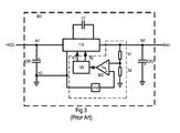
図1は、正の入力電圧(+VDD)から負の出力電圧(Vout−)を生成する先行技術の反転チャージポンプ(inverting charge-pump:ICP)回路100を示す。理想的な条件では、Vout−は、実質的に−VDDと等しく、このため、ノードN1〜N2の合計電圧が2×VDDとなる。回路100は、1つのフライングキャパシタCfおよび2つのリザーバキャパシタCR1,CR2の3つのキャパシタと、スイッチアレイ110を備える。回路100は、スイッチアレイ110を制御し、このため、回路100を、下記に説明する2つの主要状態間で切り替えさせるコントローラ120によって制御される。
FIG. 1 shows a prior art inverting charge-pump (ICP)
図2aは、ICP回路100に関連するスイッチアレイ110を示す。図2b,2cは、2つの主要な充電/放電の動作状態の等価回路を示す。スイッチSA1,SA2およびスイッチSB1,SB2は図のように配置され、それぞれ共通の制御信号(CSAおよびCSB)によって作動される。
FIG. 2 a shows the
コントローラは、電圧Vout−を生成するために、以下の4つのステップを繰り返すようにスイッチアレイ110を作動させる。
1.最初に全てのスイッチが開いている。
2.スイッチSA1,SA2を閉じ(SB1,SB2は開のまま)、これにより、ICP回路100が第1状態で動作する。フライングキャパシタCfが、(図2bに示すように)入力電圧ノードN1と共通基準電圧ノードN3間に接続される。このため、フライングキャパシタCfが電圧+VDDまで充電される。
3.次にスイッチSA1,SA2を開く(SB1,SB2は開いたまま)。
4.次にスイッチSB1,SB2を閉じ(SA1,SA2は開のまま)、これにより、ICP回路100が第2状態で動作する。この状態では、フライングキャパシタCfが、(図2cに示すように)共通基準電圧ノードN3と出力電圧ノードN2間に接続されている負のリザーバキャパシタCR2と並列に接続される。この第1のサイクルでは、最初にキャパシタCR2の充電が0ボルトであるとすると、キャパシタCR2はキャパシタCfと電荷を共有し、両キャパシタの電圧が等しくなる。キャパシタCfの陽極板とCR2の陽極板が共通基準電圧ノードN3(グランド)に接続されているため、CfとCR2のそれぞれのサイズに応じて、ノードN2は、ノードN3に対して−VDDよりやや正の電圧となる。
The controller operates the
1. First, all switches are open.
2. The switches SA1 and SA2 are closed (SB1 and SB2 remain open), whereby the
3. Next, the switches SA1 and SA2 are opened (SB1 and SB2 remain open).
4). Next, the switches SB1 and SB2 are closed (SA1 and SA2 remain open), whereby the
全てのスイッチが開き、この過程がステップ1から繰り返す。4ステップからなる各サイクルにおいて、キャパシタCR2が更に充電され、最終的に、4ステップのサイクルを複数繰り返した後に定常状態に達する。この時点までに、キャパシタCR2は、実質的に−VDDに充電され(このためVout−は−VDDと等しくなっており)、このため、Cfが、更に電荷を追加することはなくなる。
All switches open and the process repeats from
スイッチアレイ110は、上で説明したように、スイッチのスイッチング周波数が実質的に固定されている開ループ構成で作動されうる。実際のスイッチング周波数は、回路が使用されるアプリケーションによって決まり、例えば、KHz〜MHzの値(magnitude)であってもよい。
The
負荷がVout−に印加されると、これによりキャパシタCR2が常に放電される。その後、この電荷が、状態2中にキャパシタCfからの電荷によって置き換えられ、この結果、Vout−が−VDDよりも若干正となる。平均の差と電圧リプルは、Cf、CR2の値、スイッチング周波数および負荷特性に依存する。
When a load is applied to Vout-, this causes the capacitor CR2 to always be discharged. This charge is then replaced by the charge from capacitor Cf during
図3は、スイッチアレイ110が閉ループ構成で作動される別の先行技術のICP回路300を示す。この別の先行技術のICP回路300は、スイッチアレイ制御論理310が出力電圧Vout−に依存しているという点で、図1のものとは異なる。ICP回路300は、上で説明したようにスイッチアレイ110、キャパシタCf,CR1,CR2のほか、分圧器R1,R2と比較器320を備える。ノードN2上の出力電圧Vout−の調整は、内部抵抗分割器R1,R2によって出力電圧Vout−を検知し、キャパシタCR2の電圧Vout−が比較器320の基準入力Vrefよりも正になったときに、スイッチアレイ110を作動させることによって行われる。スイッチアレイ110の作動時は、2相の非重複のクロック信号K1,K2がスイッチ(図示なし)を制御する。一方のクロック信号(K1)が、フライングキャパシタCfを入力電圧+VDDまで充電させる(図2b参照)スイッチSA1,SA2を制御し、もう一方のクロック信号(K2)が、出力リザーバキャパシタCR2を電圧Vout−まで充電させる(図2c参照)スイッチSB1,SB2を制御する。
FIG. 3 shows another prior
出力電圧Vout−は、グランド電位と−VDDの間の値に調整されうるが、チャージポンプ自体は、出力電圧Vout−が−VDDと等しい場合に最も効率が高い点に留意すべきである。実際には、目標電圧は、リプルを低減させるために、おそらく−VDDよりわずかに上の値に設定される。 It should be noted that although the output voltage Vout− can be adjusted to a value between ground potential and −VDD, the charge pump itself is most efficient when the output voltage Vout− is equal to −VDD. In practice, the target voltage is probably set to a value slightly above -VDD to reduce ripple.
この先行技術のICP回路(100,300)に関連する問題として、入力電圧よりレール・ツー・レールの値の大きな出力電圧しか生成されないという点がある。この点は、特定のアプリケーションでは不利でありうる。これは、例えば、このようなICP回路(100,300)が、増幅器回路の電力供給±VDDに比べて最大振幅の極めて小さい信号を増幅するパワー回路に使用される場合などに、給電される回路が効率的に動作できないことがあるためである。 A problem associated with this prior art ICP circuit (100, 300) is that it produces only an output voltage that has a rail-to-rail value greater than the input voltage. This can be disadvantageous for certain applications. This is because, for example, when such an ICP circuit (100, 300) is used in a power circuit that amplifies a signal having an extremely small maximum amplitude compared to the power supply ± VDD of the amplifier circuit, the circuit to be fed This is because there is a case that cannot operate efficiently.
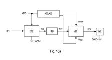
図4aは、新規のデュアルモードチャージポンプ(dual mode charge-pump:DMCP)回路400を示す。回路400は、1つのフライングキャパシタCfおよび2つのリザーバキャパシタCR1,CR2の3つのキャパシタと、スイッチアレイ410を備える。回路400は、スイッチアレイ410を制御し、このため、回路400を、下記に説明する異なる動作モードを実施するために、各種状態間で切り替えさせるコントローラ420によって制御される。クロック信号(図示せず)がコントローラに供給され、このクロック信号はDMCP400内で生成されても、あるいはチップ上のほかの回路と共有されてもよい。動作時に、回路400は、フライングキャパシタCfを使用して、正の入力電圧(+VDD)から正負の出力電圧(Vout+およびVout−)を生成するように、入力供給からリザーバキャパシタに電荷のパケット(packets
of charge)を高周波数で転送する。この出力電圧の値は、選択されたモードによって決まる。説明の便宜上、さまざまな回路ノードに名称を付し、入力供給電圧VDDを入力するように接続されたノードをN10、共通(グランド)ノードであるノードをN11、Vout+およびVout−のための出力端子をそれぞれ形成しているノードをN12,N13と呼ぶ。
FIG. 4 a shows a novel dual mode charge-pump (DMCP)
of charge) at high frequencies. The value of this output voltage depends on the selected mode. For convenience of explanation, names are given to various circuit nodes, a node connected to input the input supply voltage VDD is N10, a node that is a common (ground) node is N11, and output terminals for Vout + and Vout− N12 and N13 are nodes forming the nodes respectively.
出力Vout+,Vout−とN11(0V)に負荷450が接続されている。実際には、この負荷450は、その全体または一部が電源と同じチップに存在していても、あるいはチップの外に存在していてもよい。アプリケーションの例については、図23〜25を参照して後述する。
A
DMCP400は、名前が示すように、2つの主要モードで動作可能である。これらの全モードについて、以下で更に詳細に説明する。当然、デュアルモード回路の原理は、複数モードにも拡張することができる。
以降「モード1」と呼ぶ第1の主要モードでは、DMCP400が、入力電圧+VDDに対して、値がそれぞれ入力電圧VDDの半分である出力を生成するようにDMCP400が動作する。換言すれば、この第1モードで生成される出力電圧の値は、公称値では+VDD/2と−VDD/2となる。実際は、わずかに負荷がかかっている場合には、出力レベルは、±(VDD/2−Iload×Rload)となる(Iloadは負荷電流、Rloadは負荷抵抗)。この場合、ノードN12とノードN13間の出力電圧の大きさ(VDD)が、ノードN10とノードN11間の入力電圧(VDD)と同じか実質的に同じとなるが、シフトする。このため、このモードは、「レベルシフティング」モードと呼ぶことができる。第2の主要モード(モード2)では、DMCP400は、±VDDのデュアルレール出力を生成する。
In the first main mode, hereinafter referred to as “
チャージポンプのこの特定の形態は、特に1つのフライングキャパシタのみを使用して、降圧された(reduced)2極性の供給を生成することができるため、公知の回路と比べて大きな利点を有する。降圧された出力電圧を生成するための先行技術の回路では、追加のフライングキャパシタが必要であった。フライングキャパシタとリザーバキャパシタは、多くの場合これらをチップ外に設けなければならない位の大きさを有し、このため、1つのキャパシタと2本のICピンを省略できることは非常に有利である。本発明は、本明細書に示す特定の形態のDMCPのアプリケーションに限定されるとみなすべきではなく、公知あるいは現時点で未知のマルチモードチャージポンプ回路にも潜在的に適用可能である。 This particular form of charge pump has significant advantages over known circuits, especially because only one flying capacitor can be used to produce a reduced bipolar supply. Prior art circuits for generating a stepped down output voltage required an additional flying capacitor. Flying capacitors and reservoir capacitors are often as large as they must be provided outside the chip, and it is therefore very advantageous to be able to omit one capacitor and two IC pins. The present invention should not be regarded as limited to the particular form of DMCP application presented herein, but is potentially applicable to known or currently unknown multi-mode charge pump circuits.
図4bは、DMCP100の内部の詳細を更に詳しく示す。この図から、スイッチアレイ410は、スイッチ制御モジュール420からの対応する制御信号CS1〜CS6によって各々制御される6つのメインスイッチS1〜S6を備えることがわかる。これらのスイッチは、第1スイッチS1が、フライングキャパシタCfの陽極板と入力電圧源の間に接続され、第2スイッチS2が、フライングキャパシタの陽極板と第1出力ノードN12の間に接続され、第3スイッチS3が、フライングキャパシタの陽極板と共通端子N11の間に接続され、第4スイッチS4が、フライングキャパシタの陰極板と第1出力ノードN12の間に接続され、第5スイッチS5が、フライングキャパシタの陰極板と共通端子N11の間に接続され、第6スイッチS6が、フライングキャパシタの陰極板と第2出力ノードN13の間に接続されるように構成されている。任意選択で、入力電圧源(ノードN10)と第1出力ノードN12の間に接続された第7スイッチS7(点線で示す)が設けられてもよい。これらのスイッチは、記載するモードに適している。当然、ほかの動作モードを実現するするためにスイッチを追加することが除外されることはない。
FIG. 4b shows the internal details of
スイッチは、例えば、集積回路のプロセス技術または入出力電圧の要件に応じて、多くの異なる方法(例えば、MOSトランジスタスイッチまたはMOS伝送ゲートスイッチ)で実装することができる。適切な実装の選択は、当業者である読者の能力の十分に範囲内である。 The switches can be implemented in many different ways (eg, MOS transistor switches or MOS transmission gate switches), for example, depending on the integrated circuit process technology or input / output voltage requirements. The selection of an appropriate implementation is well within the ability of the reader of ordinary skill.
また、この図には、2つの制御機能420a,420bのいずれを使用するかを判定し、このため、DMCPの動作モードを決定するためのモード選択回路430を少なくとも概念的に有する制御モジュール420も詳細に示されている。モード選択回路430とコントローラ420a等は、DMCP400の異なる動作モードを実装する際の制御モジュールの異なる挙動を表しているという点で、概念的なブロックである。これらは、説明のように別個の回路によって実装することもできる。実際には、これらは、所定の時点で実装すべき挙動を決定する、固定配線された論理および/またはシーケンサコードを有する1つの回路ブロックあるいはシーケンサによって実装される可能性が高い。また、下記に記載するように、所定のモードが、さまざまな変形例で実装されてもよく、設計者は、異なる全モードを併せて考察する際に、制御信号の生成を簡略化する変形例を選択してもよい。
Also shown in this figure is a
DMCP動作−モード1
モード1の主要動作の実施形態では、3段階の高周波数のサイクルで繰り返される3つの基本動作状態が存在し、これらの状態をP1、P2、P3と呼ぶ。DMCP400がモード1で動作しているときは、スイッチS7(存在する場合)は常時開いており、このため、このモードの説明では記載しない。
DMCP operation-
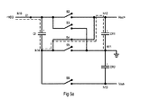
In the
図5a,5bは、第1状態(「状態1」)で動作しているスイッチアレイ410を示す。図5aを参照すると、キャパシタCfとCR1が相互に直列に、入力電圧+VDDと並列に接続されるように、スイッチS1,S4が閉じる。このため、キャパシタCfとCR1は、キャパシタCfとCR1の両端に印加された入力電圧+VDDを共有する。図5bは、電圧+VDDが、ノードN10とN11の両端に実質上印加されている状態1の動作の等価回路を示す。
5a and 5b show the
対称な逆極性の出力電圧を必要とするアプリケーションでは、各キャパシタCf,CR1が、電圧源の両端に直列に接続されたときに、電圧が同じ増分で変化するように、キャパシタCfとCR1の値が等しいことが好ましい。両キャパシタが初期状態では放電されているか、または等しい電圧に充電されている場合には、最終的には、キャパシタCf,CR1は、印加された電圧源の半分(この場合には入力電圧VDDの半分)に等しい電圧にそれぞれ充電される。 In applications that require a symmetric reverse polarity output voltage, the values of capacitors Cf and CR1 are such that when each capacitor Cf, CR1 is connected in series across the voltage source, the voltage changes in the same increment. Are preferably equal. If both capacitors are initially discharged or are charged to an equal voltage, eventually the capacitors Cf and CR1 are half of the applied voltage source (in this case the input voltage VDD Are each charged to a voltage equal to half).
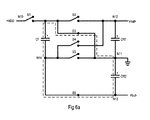
図6a,6bは、第2状態(「状態2」)で動作しているスイッチアレイ410を示す。図6aを参照すると、キャパシタCfとCR2が相互に並列に、ノードN11とN13の間に接続されるように、スイッチS3,S6が閉じる。このため、キャパシタCfの電圧は、キャパシタCR2の電圧と等しくなる。図6bは、この状態2の状態の等価回路を示す。
6a and 6b show the
リザーバキャパシタCR2の値が必ずしもフライングキャパシタCfと等しい必要があるというわけではない点に留意すべきである。キャパシタCR2がキャパシタCfよりも非常に大きな場合、VDD/2に近い値に充電されるには、多くのサイクルを要する。リザーバキャパシタCR2の値は、予想される負荷条件、必要な動作周波数、および出力リプルの許容値に応じて選択すべきである。 It should be noted that the value of the reservoir capacitor CR2 does not necessarily have to be equal to the flying capacitor Cf. If capacitor CR2 is much larger than capacitor Cf, it takes many cycles to charge to a value close to VDD / 2. The value of reservoir capacitor CR2 should be selected depending on the expected load conditions, the required operating frequency, and the output ripple tolerance.
状態1,2が交互に反復されるサイクルが複数繰り返されると、理想的な条件では、キャパシタCfの電圧とCR2の電圧が、電圧±VDD/2に収束する。しかし、チャージポンプの出力端子に大きな負荷が存在する場合には、Vout+,Voutのそれぞれの電圧が±VDDから垂下する。負荷が対称的であり、Vout+とVout−の両方の電流の大きさが等しい場合には、このようなシステムの対称性により2つの出力の垂下量が等しくなる。
When a plurality of cycles in which the
しかし、例えば、Vout+に大きな負荷が存在し、Vout−に負荷がないか負荷が軽微な場合には、キャパシタCR1の電圧が低下する。この結果、状態1の終了時点でキャパシタCfの電圧が高くなり、これが、その後、状態2でキャパシタCR2に印加される。状態1,2のみが使用されるとすれば、フライングキャパシタCfが状態1においてキャパシタCR1と直列に接続されるが、初期であるにも関わらず電圧が高くなっている。このため、電圧Vout+とVout−の両方が負に垂下してしまう。これは、つまり、コモンモードが制御されないということである。
However, for example, when there is a large load on Vout + and there is no load on Vout− or the load is light, the voltage of the capacitor CR1 decreases. As a result, the voltage of the capacitor Cf becomes high at the end of the
この影響を回避するために、第3状態の状態3を導入し、連続するサイクルで、状態1〜3が段階1〜3において繰り返される。図7a,7bは、この状態3の動作で動作しているスイッチアレイ410を示す。図7aを参照すると、状態3では、キャパシタCfとCR1が互いに並列に、ノードN11とN12間に接続されるように、スイッチS2,S5が閉じる。このため、前の電圧差の有無を問わず、キャパシタCfとCR1が、等しい電圧に充電される。定常状態(多くのサイクル後)では、この値はほぼVDD/2になる。図7bは、この状態3の状態の等価回路を示す。
To avoid this effect,
このため、回路は、状態3が終わった時点で、電圧が等しくなっており、その後状態1に戻る。このように、回路は、原理上、負荷条件とスイッチングシーケンスに応じて、Vout+=+VDD/2で次のサイクルの状態1の段階1に入る。
Thus, the circuit is equal in voltage at the end of
実際には、特にDMCPのRC時定数に対してスイッチング周波数が高い場合には、状態2,3において、並列に接続されたキャパシタ間の電圧が、1回のシーケンスで完全には等しくならないことがある。この場合は、各状態シーケンスにおいて、電荷の寄与が、キャパシタからキャパシタに移される。この寄与により、各出力電圧が、ゼロを下回るかまたは低い負荷条件のレベルに設定される。高負荷条件下では、出力リザーバキャパシタCR1,CR2は、通常、低電圧(若干のリプルを含む)となる。各キャパシタの大きさを、予想されるあらゆる負荷条件に対して、コモンモードのドリフトの低下が許容される幅に入るように設計するだけでよい。あるいは、これに代えて、またはこれに加えて、オン抵抗(on-resistance)の小さい大きなスイッチを使用してもよい。
In practice, especially when the switching frequency is high with respect to the RC time constant of DMCP, in
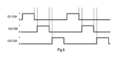
図8は、モード1の主要動作の実施形態の3状態(1,2,3)中にスイッチ(S1 〜S6)を制御するための非重複の制御信号(CS1〜CS6)を示す。上で説明したように、これは、多くの可能な制御シーケンスの一例を例示するに過ぎない。
FIG. 8 shows non-overlapping control signals (CS1-CS6) for controlling the switches (S1-S6) during the three states (1, 2, 3) of the
上記の3状態の開ループシーケンスが必ずしも必要であるというわけではないことが理解されるべきである。例えば、状態シーケンスは、(上記の)1、2、3、1、2、3…でも、1、3、2、1、3、2…でも、1、2、1、3、1、2、1、3でもよい。また、第3状態が他の2つの状態ほど頻繁に使用する必要はなく、例えば、1、2、1、2、1、2、3、1のシーケンスが想到されることが明らかであろう。更には、負荷のバランスが良好な場合、あるいは、コモンモード安定化のための別の方式が使用されている場合に限り、第3状態を完全に省略することも想到される。
It should be understood that the above three-state open loop sequence is not necessarily required. For example, the state sequence can be 1, 2, 3, 1, 2, 3 ... (above), 1, 3, 2, 1, 3, 2, ..., 1, 2, 1, 3, 1, 2,. 1, 3 may be sufficient. It will also be apparent that the third state does not need to be used as frequently as the other two states, for example, the
ほかのスイッチングおよびシーケンスも存在する。例えば、動作モード1の別の一実施形態では、状態1に代えて、スイッチS1,S5が閉じる(他の全スイッチは開)第4状態(「状態4」)が使用されてもよい。この状態では、キャパシタCfが、入力電圧+VDDに充電される。次に、第5状態である「状態5」において、フライングキャパシタCfが、リザーバキャパシタCR1およびCR2の両端に直列に(この場合、キャパシタンスが等しい)接続されるように、スイッチS2,S6が閉じて(他の全スイッチは開)作動する。この別のスイッチングおよびシーケンスの特定の例は、コモンモードが制御されないという欠点を有し、このためコモンモードのドリフトが発生する。しかし、このコモンモードドリフトは、「通常の」スイッチングおよびシーケンスサイクル中に、適切な間隔でスイッチングシーケンスを変更することによって「リセット」することができる。この変更は、事前に決定されても、観察された状態に応じて開始されてもよい。
Other switching and sequences exist. For example, in another embodiment of the
キャパシタCf,CR1,CR2のサイズは、(サイズ/コストに対する)要求されるリプル許容値に応じて選択され、このため、各状態のクロック段階の時間の長さの比が、必ずしも1:1:1である必要はないという点に留意すべきである。 The size of the capacitors Cf, CR1, CR2 is selected according to the required ripple tolerance (relative to size / cost), so that the ratio of the time lengths of the clock phases in each state is not necessarily 1: 1: It should be noted that it need not be 1.
上記は、モード1で±VDD/2の出力が生成される実施形態について説明したが、上記の教示は、フライングキャパシタCfの個数を増やし、これに応じてスイッチ網を変更することによって、VDDの任意の分数出力を得るために使用できることを当業者は理解するであろう。この場合には、出力と入力の関係は、Vout+/−=±VDD/(n+1)となる(nはフライングキャパシタCfの個数)。また、記載の複数のフライングキャパシタを有する回路は、±VDD/2の出力のほか、その制御に応じて、±VDD/2〜±VDD/(n+1)間のあらゆる整数分母の出力を生成するもできる。例えば、2つのフライングキャパシタを有する回路はVDD/3とVDD/2の出力を生成することができ、3つのフライングキャパシタを有する回路はVDD/4、VDD/3、およびVDD/2の出力を生成することができるなどである。
The above describes an embodiment in which an output of ± VDD / 2 is generated in
DMCP動作−モード2
上で述べたように、DMCPは、±VDD(この場合も、+VDDはノードN10における入力源電圧レベルである)のデュアルレール出力を発生させる第2の主要モード(モード2)でも動作可能である。モード2では、スイッチS4は、常に開いている。
DMCP operation-
As mentioned above, DMCP is also operable in the second main mode (mode 2) which generates a dual rail output of ± VDD (again, + VDD is the input source voltage level at node N10). . In
モード2のいくつかの変形例が可能であり、これらをモード2(a)、2(b)、2(c)、2(d)と称し、下に後述する。任意選択のスイッチS7は、モード2(c),2(d)のために必要である。
Several variations of
モード2(a)では、DMCPは、2つの基本動作状態を有する。図9aは、これらの状態の1つである「状態6」で動作している回路を示す。この状態では、スイッチS1,S2,S5が閉じる(S3,S4,S6は開)。この結果、キャパシタCfとCR1が、ノードN10およびN11間で入力電圧+VDDと並列に接続される。このため、キャパシタCfとCR1は、それぞれ入力電圧+VDDを保持する。図9bは、この状態6の状態の等価回路を示す。
In mode 2 (a), DMCP has two basic operating states. FIG. 9a shows a circuit operating in “
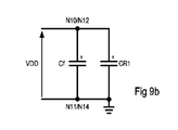
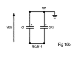
図10aはこれらの状態の第2状態で動作中の回路を示す。この状態は、実際にはモード1の状態2と同じ状態であり、スイッチS3,S6が閉じる(S1、S2、S4,S5は開)。このため、キャパシタCfとCR2は、共通ノードN11と第2出力ノードN13間に並列に接続される。このため、キャパシタCfとCR2は、互いの電荷を共有し、所定のサイクル後、ノード13が電圧−VDDとなる。図10bは、この状態2の状態の等価回路を示す。
FIG. 10a shows the circuit operating in the second of these states. This state is actually the same state as
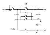
図12aは、追加の状態である「状態7」を示す。この状態は、ここでモード2(b)と呼ぶわずかに異なる実装を作るために、モード2(a)のシーケンスに導入することができる。状態7では、スイッチS1,S5が閉じる(S2,S3,S4,S6は開)。この状態7は、フライングキャパシタCfを入力電圧+VDDの両端に接続する。この状態の後に状態6と状態2が続き、再び状態7に戻りうる。図12bは、この状態7の状態の等価回路を示す。
FIG. 12 a shows “
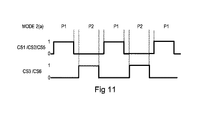
図13は、スイッチ(S1〜S3およびS5〜S7)を制御して、モード2(b)を定義する3状態7、6、2、7、6、2…などの反復シーケンスを生成するための非重複の制御信号(CS1〜CS3およびCS5〜CS7)を示す。この場合も、これは、多くの可能な制御シーケンスの一例を例示するに過ぎない。状態6の前に状態7を入れているのは、CR1をCR2の影響から隔離して、相互調整(cross-regulation)を阻止することを意図している。一方で、状態7を入れることにより、主要な状態2と状態6において電荷転送に使える時間が短くなるため、状態7を単に省略することにより(モード2(a))、全体としての調整が改善されうる。これらは設計事項である。
FIG. 13 controls the switches (S1-S3 and S5-S7) to generate a repetitive sequence of three
いずれのパターンを選択する場合であっても、(モード1に関して上で説明したように)状態の1つが他の状態よりも使用頻度が低くてもよい。例えば、(恒久的に、あるいは信号状態により)2つの出力ノードN12,N13の負荷の均衡が崩れた場合、キャパシタCR1はキャパシタCR2ほど頻繁に充電が必要でなくなるか、この逆の状況となるため、状態6と状態2の一方は、もう一方の状態よりも使用頻度低くてもよい。
Whichever pattern is selected, one of the states may be used less frequently than the other states (as described above with respect to mode 1). For example, if the load balance of the two output nodes N12, N13 is lost (permanently or due to signal conditions), the capacitor CR1 will not need to be charged as frequently as the capacitor CR2, or vice versa. One of
モード2(c)とモード2(d)は、±VDDを生成するための更に別の動作モードであり、DMCPにスイッチS7が設けられている場合に可能である。このスイッチは、ハイサイドの負荷(すなわちノードN12とN11間に接続された負荷)が、多くの電流を必要としないアプリケーションにおいて、ノードN12で正の出力電圧を生成するために、スイッチS1とS2を併せた機能の代わりとして使用されうる。これは、例えばミキサーの「ライン出力」のように、負荷が高い入力抵抗を有する場合などである。このような場合、スイッチS7のサイズと駆動要件は、スイッチS1,S2よりも下げ、変更することができる。実際、スイッチS7は、モード2(c)の動作中は、常時オンであり、この点は、スイッチを駆動するために必要な電力が少なくて済み、スイッチS7は、MOSスイッチの実装の場合、そのゲート−ドレインおよびゲート−ソースの寄生キャパシタンスのため、ノードN10またはN12に電荷を注入することがないという点で有利である。また、スイッチS1は、負出力電圧−VDDを生成するように作動させる必要があるという点にも留意すべきである。更に、フライングキャパシタCfとハイサイドのリザーバキャパシタCR1を並列に接続するために、スイッチS2がさほど頻繁ではないにせよ、作動されうる点にも留意すべきである。 Mode 2 (c) and mode 2 (d) are still other operation modes for generating ± VDD, and are possible when the switch S7 is provided in the DMCP. This switch is connected to switches S1 and S2 to generate a positive output voltage at node N12 in applications where the high side load (ie, the load connected between nodes N12 and N11) does not require much current. Can be used as an alternative to the combined function. This is the case, for example, when the load has a high input resistance, such as the “line output” of the mixer. In such a case, the size and driving requirements of the switch S7 can be lowered and changed from those of the switches S1 and S2. In fact, the switch S7 is always on during the operation of the mode 2 (c), and this point requires less power to drive the switch. The gate-drain and gate-source parasitic capacitances are advantageous in that no charge is injected into node N10 or N12. It should also be noted that the switch S1 needs to be activated to generate the negative output voltage -VDD. It should also be noted that the switch S2 can be actuated, if less frequently, to connect the flying capacitor Cf and the high-side reservoir capacitor CR1 in parallel.
図14は、モード2(c)の2つの交互の状態中に、スイッチ(S1〜S3およびS5〜S7)を制御するための非重複の制御信号(CS1〜CS3およびCS5〜CS7)を示す。このため、モード2(c)をまとめると、スイッチS7は恒久的に(またはほぼ恒久的に)閉じている。フライングキャパシタCfとキャパシタCR1を並列に充電するために変更された状態6が使用され、これは、スイッチS1,S5,S7を閉じるだけで行われる。次に、上で説明したように、スイッチS3,S6を介してこの電荷をキャパシタCR2に転送するために変更された状態2が使用されるが、この場合は、S7が閉じているため、キャパシタCR1に電圧VDDが保持されている。
FIG. 14 shows non-overlapping control signals (CS1 to CS3 and CS5 to CS7) for controlling the switches (S1 to S3 and S5 to S7) during the two alternating states of mode 2 (c). For this reason, when mode 2 (c) is put together, the switch S7 is permanently (or almost permanently) closed. A modified
図15は、モード2(d)と呼ぶ、モード2(c)の変形例の3状態中に、スイッチ(S1〜S3およびS5〜S7)を制御するための非重複の制御信号(CS1〜CS3およびCS5〜CS7)を示す。モード2(c)との違いは、状態7にスイッチによる追加の段階が追加されているという点で、モード2(a)と2(b)の差と同様である。状態7では、スイッチS1およびS5は閉じる(S2、S3、S4およびS6は開き、S7は常に閉じてもよい)。モード2(d)は、7、6、2ではなく、7、2、6、7、2、6…というシーケンスを辿る点に留意されたい。これらのモードには、必ずしも効果に大きな違いがあるというわけではないが、下記で説明するように、シーケンスを自由に変更できることにより、制御論理を簡略化することができる。
FIG. 15 shows non-overlapping control signals (CS1 to CS3) for controlling the switches (S1 to S3 and S5 to S7) during the three states of the modification of mode 2 (c), referred to as mode 2 (d). And CS5 to CS7). The difference from mode 2 (c) is the same as the difference between modes 2 (a) and 2 (b) in that an additional stage by a switch is added to

表1は、上に説明した7つの状態に対するスイッチ(S1〜S7)の状態を示し、「0」はスイッチの開を、「1」はスイッチの閉を表している。特定の実装で、記載したモードのサブセットが使用される限り、スイッチ網とコントローラは、状態1〜7の全てを必ずしも実装しなくても点に留意されたい。 Table 1 shows the states of the switches (S1 to S7) for the seven states described above, where “0” represents opening of the switch and “1” represents closing of the switch. Note that the switch network and controller do not necessarily implement all of states 1-7 as long as a particular implementation uses a subset of the described modes.
この場合も、これらの4つのシーケンスの例と、スイッチ網の7〜8の異なる状態は、唯一可能なシーケンスの制御ではない。この場合も、多くの異なるシーケンスの実装が可能であり、これらの状態は、負荷に応じて、他よりも使用頻度が低くてもよい。 Again, these four sequence examples and the 7-8 different states of the switch network are not the only possible sequence controls. Again, many different sequences can be implemented, and these states may be used less frequently than others, depending on the load.
図16は、図4に示したものと同様のDMCP900回路を示すが、DMCP900が、2つの出力電圧を調整するための2つの比較器910a,910bも備える点が異なる。
FIG. 16 shows a
DMCP900が閉回路DMCPを表している点に留意すべきである。比較器910a,910bの各々は、チャージポンプ出力電圧(Vout+,Vout−)のそれぞれを、個々のしきい値電圧(Vmin+、Vmin−)と比較し、電荷信号CHCR1,CHCR2をそれぞれ出力する。これらの電荷信号CHCR1,CHCR2は、スイッチアレイ1410を制御して、関連するリザーバキャパシタを充電するようにDMCPを作動させるために、スイッチ制御モジュール1420に供給される。一方の出力電圧が、そのしきい値を越えて垂下している場合、チャージポンプが作動され、垂下していない場合には、チャージポンプは一時停止される。これにより、特に低負荷の条件において、スイッチの切換に消費されるパワーを低減することができる。
Note that
この方式により、最大±VDD/2の出力電圧が可能となる。更に、この構成においては、DMCP900が、これよりも高電圧を生成するために使用されてもよいが、効率が低下する点にも留意すべきである。この場合、出力電圧を適宜調整するために、基準電圧(Vmin+/Vmin)が調整されうる。フライングキャパシタCfは、(スイッチS1,S5を介して)+VDDに充電され、次に、(スイッチS2,S5を介して)リザーバキャパシタCR1、または(スイッチS3,S6を介して)リザーバキャパシタCR2の両端に並列に接続され、これらの電圧が基準電圧によって設定されたレベルに昇圧される。このような動作はリザーバキャパシタCR1,CR2上のリプル電圧を増加させるものの、スイッチング損失を低減する。しかし、充電キャパシタCfに対してリザーバキャパシタCR1,CR2をスケール調整(scaling)することによって、リプル電圧を低減することができる。
With this method, a maximum output voltage of ± VDD / 2 is possible. Furthermore, it should be noted that in this configuration,
図17は、上に記載した新規のデュアルモードチャージポンプ400,900のいずれかの更に別の実施形態を示し、多くの異なる入力電圧値の1つが、DMCP400,900への入力電圧として選択されうる。この図には、入力セレクタ1000が、多くの異なる電圧入力(+Vin1〜+VinN)を有し、選択される実際の入力が、制御入力Icによって決定されることが示されている。選択された電圧レベルは、その後、デュアルモードチャージポンプ400,900の入力電圧VDDとなる。
FIG. 17 illustrates yet another embodiment of any of the novel dual mode charge pumps 400, 900 described above, where one of many different input voltage values can be selected as the input voltage to the
図18aは、本明細書に記載のチャージポンプ400,900によってデュアルレール供給電圧Vout+およびVout−が生成される代表的なアプリケーションを示し、チャージポンプ400,900は、例えばシングルレール供給電圧VDDから供給を受ける。別の実施形態では、図17に示すように、チャージポンプ400,900が複数の供給電圧によって供給を受けてもよい。VDD、Vout+などの記号は、図18a,18bに関連する説明において解釈すべきであり、文脈に応じて、個々の端子またはその端子における電圧を指す。 FIG. 18a illustrates a typical application in which dual rail supply voltages Vout + and Vout− are generated by charge pumps 400, 900 described herein, which are supplied from, for example, a single rail supply voltage VDD. Receive. In another embodiment, as shown in FIG. 17, the charge pumps 400, 900 may be supplied with multiple supply voltages. Symbols such as VDD, Vout +, etc. should be construed in the description associated with FIGS. 18a, 18b and refer to an individual terminal or voltage at that terminal, depending on the context.
図18aを参照すると、供給電圧VDDは、処理回路20に供給するものとして示される。入力信号S1は、アナログ信号でもデジタル信号でもよい。S1がアナログ信号の場合、処理回路20は、オペアンプ、マルチプレクサ、ゲインブロックなどの純粋なアナログ型回路である。S1がデジタル信号であり、出力段がアナログである場合は、処理回路20はデジタルとアナログの混合回路であってもよい。この場合、信号S1は、直接または何らかのデジタル信号処理を介して、DAC(図示なし)に供給され、DACの出力が、上で述べたようにアナログ回路に供給される。
Referring to FIG. 18a, the supply voltage VDD is shown as being supplied to the
処理回路20は、処理された信号S2を出力し、信号S2は、この特定の実施形態では、レベルシフタ30に渡されるアナログ信号である。レベルシフタ30は、例えばDCブロッキングキャパシタによって実装されてもよい。出力増幅器40は、チャージポンプ400,900によって生成されるデュアルレール供給電圧Vout+,Vout−によって給電され、このレベルは、特定の実施形態では、チャージポンプ400,900の動作モードに応じて、±VDDまたは±VDD/2である。チャージポンプ400,900の動作モードは、制御信号Cnlによって決定される。モード1は、ヘッドフォンなどの低インピーダンス負荷を駆動するために使用され、モード2は、ライン出力などの高インピーダンス負荷を駆動するために使用されうる。モード選択は、例えば、音量設定レベルまたはコードによって手動で行われても、あるいは、ポータブルオーディオデバイスの場合には、出力インピーダンスまたは出力電流供給、またはジャックソケットとドッキングステーションのいずれが使用されているかを自動的に検知して行われうる。チャージポンプをモード2に設定する「モード選択」に音量制御が使用される場合、音量が高に設定されると、通常の状況では、負荷の電力所要量がチャージポンプ400,900の設計値よりも大きいため、出力供給電圧が崩壊しうる。しかし、このような状態を監視して、回路のチャージポンプ400,900または別の部品をオフにするために、(例えば、危険なほど高い音量により、耳が損傷を受けないように保護するための)追加の回路の形の保護(図示なし)が設けられてもよい。
The
入力信号S1がアナログであり、処理回路20中のアナログ信号である場合は、通常、グランド電位とVDDの中間の値で参照される一方、分割レール供給Vout+,Vout−から動作している出力増幅器によって要求されるように、レベルシフトされた信号S2’はグランドに対して参照される。
If the input signal S1 is analog and is an analog signal in the
レベルシフトされた信号S2’は、出力増幅器40に供給され、出力増幅器40は、増幅出力信号S3を出力し、これが、信号トランスデューサ50の形のグランド基準負荷に供給される。出力増幅器40が、スイッチング(クラスDまたはPWM)増幅器または1ビットデジタル(シグマ−デルタ)タイプの出力段である場合には、信号S1,S2は、入力から出力まで(right
through to input to output)デジタル信号形式であっても、最初はアナログ形式であるが、処理回路20でデジタル形式に変換されてもよい。
The level shifted signal S2 ′ is supplied to an
through to input to output) Even if it is in a digital signal format, it is initially in an analog format, but may be converted into a digital format by the
図18bは、図18aの構成の特定のアプリケーションを示し、簡潔を期するために、チャージポンプ400,900と供給用の接続が省略されている。本例では、アプリケーションは、負荷がステレオヘッドフォン51であるステレオ増幅器である。増幅器の信号処理要素は、参照符号の添え字「L」および「R」によって示すように、左右のチャネル信号を処理するために重複して設けられている。供給電圧Vout+およびVout−は、両方のチャネルによって共有されてもよいが、アプリケーションが要求する場合には、異なるチャネルにそれぞれ供給することも可能である。アプリケーションの一分野は、例えば、分割レール供給によりDCカップリングされた出力が可能になるMP3プレーヤなどのポータブルオーディオ装置であり、この場合、大型のデカップリングコンデンサを使用する必要なく、低音応答を保持することが望ましい。 FIG. 18b shows a particular application of the configuration of FIG. 18a, and the supply connections with the charge pumps 400, 900 are omitted for the sake of brevity. In this example, the application is a stereo amplifier whose load is a stereo headphone 51. The signal processing elements of the amplifier are duplicated to process the left and right channel signals, as indicated by the reference signs “L” and “R”. Supply voltages Vout + and Vout− may be shared by both channels, but can be supplied to different channels, respectively, if the application requires it. One area of application is portable audio devices such as MP3 players that allow DC-coupled output with a split rail supply, in which case the bass response is maintained without the need for large decoupling capacitors It is desirable to do.
図19a,19bは、2つの構成で使用されているポータブル電子機器を示し、各構成に対して出力段に適切なレベルで電力を供給するために、上のDMCPの実施形態のいずれかを有利に適用することができる。 FIGS. 19a and 19b show portable electronics used in two configurations, and may benefit from any of the above DMCP embodiments in order to power the output stage at an appropriate level for each configuration. Can be applied to.
図19aは、1組のヘッドフォン2を駆動するために接続された第1の構成のポータブル電子オーディオ装置1を示す。図中の装置1はMP3プレーヤであるが、同じ機能が、電話機、マルチメディアプレーヤ、ラップトップコンピュータ、PDAなどに搭載されてもよい。ヘッドフォン2は、出力ジャック4に差込まれたリード線3を介して装置に接続される。装置の本体が、1つ以上の小型のラウドスピーカー(図示せず)を備えてもよく、このスピーカーは、代替の音声出力トランスデューサとして駆動されてもよいが、本説明での説明のためには、原則としてヘッドフォンと均等である。公知のように、小型軽量化とバッテリ寿命の最大化が、この市場において高度な製品(premium
products)の鍵を握る属性である。製造コストは、市場全体で重要な要素である。
FIG. 19 a shows a portable
product) is the key attribute. Manufacturing costs are an important factor throughout the market.
図19bは、ヘッドフォンが接続されない第2の構成の同じ装置1を示す。ヘッドフォンの代わりに、装置が別個のコネクタを介してドッキングステーション5に接続され、ドッキングステーション5が大型のラウドスピーカー6L,6Rを駆動する。ドッキングステーション5には、ポータブルデバイス自体よりもハイパワーの増幅器と、別個の電源(通常、主電源供給される(mains-powered))とが搭載されている。図19cは、ヘッドフォンジャック4に差込まれたラインリード線9を介して、ヘッドフォンではなく、外部増幅器7とラウドスピーカー8L,8Rが接続されている、第2の構成の同じ装置の変形例を示す。
FIG. 19b shows the
装置1は、これらの構成において、大きく異なる負荷を駆動する必要がある。ヘッドフォンまたはラウドスピーカーのインピーダンスは通常、32オーム以下である。この負荷に対して、例えば、RMSが100mVの出力振幅により、30mWの電力に対応して、フルスケールから中程度の(例えば−12dB)音量が供給される。第2の構成において、大型の増幅器のライン入力を駆動する際には、負荷インピーダンスは、通常10キロオーム以上であり、最高の品質を得るには、RMSが2Vのフルスケール信号振幅(0dB)が適切である。第1の構成でソケットを駆動する出力段が、RMSが2Vの信号を供給することができる場合、その供給電圧は2Vを越えなければならない。同じ出力段から構成1においてヘッドフォン負荷を駆動する際には、供給電圧が、出力段のトランジスタで100mVのレベルに減圧されるため、出力段の電力消費の大半が、熱の形で放散してしまう。設計者が、バッテリの長寿命化のために、ライン出力にフルの2VのRMSを供給しないことを選択すると、信号劣化が発生してしまう。
In these configurations, the
要求事項がこのように競合する結果、この市場の高度な製品では、従来は、ヘッドフォン/スピーカー負荷2を駆動するための出力段と、ドッキングコネクタ4を介したラインアウト用の別の出力段を供給する習慣が採用されてきた。各出力段は、電圧範囲に適した電力供給から駆動され、各アプリケーションの電力効率と品質が維持される。いうまでもなく、別個の出力段と、そのための別個の電源が必要となることにより、装置が大型化し、コストが増大するため、望ましくない。
As a result of these competing requirements, advanced products in this market have traditionally had an output stage for driving the headphone /
DMCPは、このような装置1に搭載することができ、別個の出力段を不要とする。代わりに1つの出力段が設けられ、その電源としてDMCPが使用される。この実施形態では、DMCPは、装置がヘッドフォン負荷を駆動する場合にはモード1で動作し、ラインアウトによって別の増幅器を駆動する場合にはモード2で動作するように構成されうる。
The DMCP can be mounted on such a
理想的には、DMCPは、装置の構成に応じて、自動的に適切なモードで動作するようにされうる。第2の構成でヘッドフォンジャック4とは別のドッキングコネクタを使用する(図19b)場合、DMCPの制御回路は、ドッキング状態を示す一般信号から、採用すべきモードを直接決定することができる。第1の構成と同様にジャック4が第2の構成で使用される場合、モード選択は複数の方法で決定されうる。第1の選択肢として、ユーザがスイッチまたはメニューオプションを利用して、音声出力モードかライン出力モードかを明示的に選択してもよい。あるいは、ボリュームコントロールをフルスケールに変えたときに、ヘッドフォンは実際には最大レベルで使用されることがないという仮定に基づいて、ユーザ設定が暗黙的に行われてもよい。あるいは、ポータブルオーディオデバイスの場合には、出力インピーダンスまたは出力電流供給、またはジャックソケットとドッキングステーションのいずれが使用されているかを自動的に検知することも可能である。
Ideally, DMCP can be made to automatically operate in the appropriate mode depending on the configuration of the device. When a docking connector other than the
分割レール供給を生成できる機能を利用可能なアプリケーションの分野としては、以下が挙げられる。
(1)アナログコンポジットビデオ信号を処理する回路用の電圧供給。グランド参照のDCカップリングされた出力信号により、黒色レベルの垂下が回避される。
(2)データリンクまたはモデム(例えばADSL)用のラインドライバ。グランド参照のDCカップリングされた出力信号により、ベースラインワンダーの影響を低減することができる。
Application areas that can utilize the ability to generate a split rail supply include:
(1) Voltage supply for circuits that process analog composite video signals. The ground-referenced DC coupled output signal avoids black level droop.
(2) Line driver for data link or modem (eg ADSL). The ground-referenced DC coupled output signal can reduce the effects of baseline wander.
コスト上とサイズ上の理由により、少ない数の集積回路に、MP3プレーヤ、携帯電話または任意の他のアプリケーションの機能を集積化できることが重要である。このため、機能回路20,30,40等と共に、供給電圧生成用の回路(この場合にはチャージポンプ400,900)を集積化することが有利である。一般に、チャージポンプ400,900のキャパシタは、チップのピン本数と、回路全体のサイズにより、現実的には集積化できず、チップの外に配置する必要がある。多くの回路は、二重極性の供給(分割レール供給)を必要とするため、必要な出力電圧ごとに1つのキャパシタを使用するのではなく、1つのキャパシタを使用して、2(または3以上)の出力電圧供給を生成することができる電圧生成回路の開発が促されてきた。
For cost and size reasons, it is important to be able to integrate the functions of an MP3 player, mobile phone or any other application in a small number of integrated circuits. For this reason, it is advantageous to integrate a circuit for generating a supply voltage (in this case, charge pumps 400 and 900) together with the
制御方式、コントローラの形態のほか、スイッチ網の明細についても、数多くのほかの変更が可能である。添付の請求の範囲に記載の本発明の趣旨および範囲から逸脱することなく、これらの回路に上記の変更および追加や、その他の変更および追加を行うことができることを、当業者は理解するであろう。したがって、上記の実施形態は、本発明の範囲を限定するものではなく、例示のために提示するものである。本明細書と請求の範囲を解釈するために、「含む、有する、備える」との文言は、請求項に挙げた要素またはステップ以外の存在を除外するものではなく、要素が、複数存在することを除外するものではなく(文脈上別の意味に解すべき場合を除く)、1つの要素が、請求項に記載の複数の要素の機能を果たしてもよいことを読者は留意すべきである。請求項に記載の参照符号は、その範囲を限定するものと解釈されるべきではない。 Many other changes can be made to the details of the switch network as well as the control scheme and controller configuration. Those skilled in the art will appreciate that these and other changes and additions may be made to these circuits without departing from the spirit and scope of the invention as set forth in the appended claims. Let's go. Accordingly, the above embodiments are not intended to limit the scope of the invention, but are presented for illustration. For the purpose of interpreting the specification and the claims, the phrase “comprising, including, comprising” does not exclude the presence of elements other than the elements or steps listed in the claims, and there are multiple elements. The reader should note that one element may serve the function of several elements recited in the claims (except where the context requires otherwise). Any reference signs in the claims should not be construed as limiting the scope.
請求項に、要素が「接続されている」または「接続のために」と記載されている場合、このような文言は、ほかの要素を除外する直接接続を必要とすると解釈すべきではなく、これらの要素が記載の機能を行うことができるのに十分な接続を指す。良好な実際的な設計においては、例えば、ここに記載しなかった起動およびシャットダウン機能、検知機能、故障保護などを実行する多くの補助的な構成要素が含まれてもよいことを当業者は理解するであろう。これらの一部については上で説明しており、いずれも、請求項に記載した各種実施形態において、本発明に特徴的な基本的な機能が損なわれるものではない。 Where the claim states that an element is “connected” or “for connection”, such language should not be construed as requiring a direct connection to exclude other elements, These elements refer to connections that are sufficient to perform the described functions. Those skilled in the art will appreciate that a good practical design may include many auxiliary components that perform, for example, startup and shutdown functions, detection functions, fault protection, etc. not described herein. Will do. Some of these are described above, and none of the basic functions characteristic of the present invention are impaired in the various embodiments described in the claims.
Vout+,Vout−およびVDDなどの記号は、上記の説明にわたって解釈されるべきであり、文脈に応じて、個々の端子またはその端子における電圧を指す。 Symbols such as Vout +, Vout− and VDD should be construed throughout the description above and refer to an individual terminal or the voltage at that terminal, depending on the context.
本発明は、チャージポンプ回路自体の変形および変更に加えて、図15に示したヘッドフォン増幅器のアプリケーションのほか、チャージポンプを搭載した装置およびシステムを全て含む。回路は、通信装置を含むあらゆる形態の(all
manner of)装置の出力段に給電するために使用することができ、この場合、出力段は、アンテナまたは伝送ライン、電気光学式トランスデューサ(発光装置)または電気機械式トランスデューサを駆動しうる。
The present invention includes all devices and systems equipped with a charge pump, in addition to the application of the headphone amplifier shown in FIG. The circuit can be any form (including all communication devices)
manner of) can be used to power the output stage of the device, where the output stage can drive an antenna or transmission line, an electro-optic transducer (light emitting device) or an electromechanical transducer.
Claims (50)
状態シーケンスにおいて前記異なる端子間にフライングキャパシタを接続し、前記入力供給から前記リザーバキャパシタに、直接または前記フライングキャパシタを介して電荷のパケットを繰り返し転送し、これにより、選択された動作モードに応じて、合計して前記入力電圧にほぼ等しい電圧になり、かつ前記共通端子の前記電圧を中心とする正負の出力電圧か、それぞれが実質的に前記入力供給に達する正負の出力電圧を有する前記分割レール供給を生成するステップを有する方法。 A method of generating a split rail voltage supply from a single input supply input at both ends of an input terminal and a common terminal, wherein the split rail supply includes individual first and second loads and individual first reservoirs. Output to a first output terminal and a second output terminal connected to the common terminal via a capacitor and a second reservoir capacitor, the method comprising:
Connecting a flying capacitor between the different terminals in a state sequence and repeatedly transferring a packet of charge from the input supply to the reservoir capacitor directly or via the flying capacitor, thereby depending on the selected operating mode The divided rails having a positive or negative output voltage centered on the voltage of the common terminal, or a positive or negative output voltage that substantially reaches the input supply. A method comprising the step of generating a supply.
入力電圧への接続のための入力端子および共通端子と、
前記複数の出力電圧を出力するための第1出力端子および第2出力端子と、前記第1出力端子および第2出力端子は、使用時に、個々の第1負荷および第2負荷と、個々の第1リザーバキャパシタおよび第2リザーバキャパシタとを介して前記共通端子に接続され、
1つのフライングキャパシタへの接続のための第1フライングキャパシタ端子および第2フライングキャパシタ端子と、
前記端子間を相互接続するために、複数の異なる状態で動作可能なスイッチ網と、
前記スイッチ網を前記異なる状態のシーケンスで作動させるためのコントローラと、を有し、
前記コントローラは、第1モードと第2モードで動作可能であり、前記モードの前記第1モードでは、前記状態に応じて、前記入力供給から前記リザーバキャパシタに、前記フライングキャパシタを介して電荷のパケットを転送し、これにより、合計して前記入力電圧にほぼ等しい電圧になり、かつ前記共通端子の前記電圧を中心とする正負の出力電圧が生成されるように適合されている回路。 A charge pump circuit for providing a plurality of output voltages,
An input terminal and a common terminal for connection to the input voltage;
In use, the first output terminal and the second output terminal for outputting the plurality of output voltages, the first output terminal and the second output terminal, respectively, are used as individual first loads and second loads, and individual first loads. Connected to the common terminal through a first reservoir capacitor and a second reservoir capacitor;
A first flying capacitor terminal and a second flying capacitor terminal for connection to one flying capacitor;
A switch network operable in a plurality of different states to interconnect the terminals;
A controller for operating the switch network in the sequence of the different states;
The controller is operable in a first mode and a second mode, and in the first mode of the mode, according to the state, a packet of charge via the flying capacitor from the input supply to the reservoir capacitor , Thereby summing to a voltage approximately equal to the input voltage and adapted to generate a positive and negative output voltage centered on the voltage at the common terminal.
前記入力端子を前記第1フライキャパシタ端子に接続するための第1スイッチ(S1)と、
前記第1フライキャパシタ端子を前記第1出力端子に接続するための第2スイッチ(S2)と、
前記第1フライキャパシタ端子を前記共通端子に接続するための第3スイッチ(S3)と、
前記第2フライキャパシタ端子を前記第1出力端子に接続するための第4スイッチ(S4)と、
前記第2フライキャパシタ端子を前記共通端子に接続するための第5スイッチ(S5)と、
前記第2フライキャパシタ端子を前記第2出力端子に接続するための第6スイッチ(S6)と、を有する請求項24〜40のいずれか1項に記載の回路。 The switch network is
A first switch (S1) for connecting the input terminal to the first fly capacitor terminal;
A second switch (S2) for connecting the first fly capacitor terminal to the first output terminal;
A third switch (S3) for connecting the first fly capacitor terminal to the common terminal;
A fourth switch (S4) for connecting the second flycapacitor terminal to the first output terminal;
A fifth switch (S5) for connecting the second flycapacitor terminal to the common terminal;
41. The circuit according to any one of claims 24 to 40, comprising a sixth switch (S6) for connecting the second flycapacitor terminal to the second output terminal.
入力電圧への接続のための入力端子および共通端子と、
前記複数の出力電圧を出力するための第1出力端子および第2出力端子と、前記第1出力端子および第2出力端子は、使用時に、個々の第1負荷および第2負荷と、個々の第1リザーバキャパシタおよび第2リザーバキャパシタとを介して前記共通端子に接続され、
複数のフライングキャパシタへの接続のための複数の第1フライングキャパシタ端子および第2フライングキャパシタ端子と、
前記端子間を相互接続するために、複数の異なる状態で動作可能なスイッチ網と、
前記スイッチ網を前記異なる状態のシーケンスで作動させるためのコントローラと、を有し、
前記コントローラは、第1モードおよび第2モードにおいて動作可能であり、前記モードの前記第1モードでは、前記シーケンスは、前記状態に応じて、前記入力供給から前記リザーバキャパシタに、前記フライングキャパシタを介して電荷のパケットを転送し、これにより、実質的に前記入力電圧の分数の値の正負の出力電圧が生成されるように適合されており、前記入力電圧の前記分数が実質的に1/(n+1)である(nは、フライングキャパシタの個数を表す整数)回路。 A charge pump circuit for providing a plurality of output voltages,
An input terminal and a common terminal for connection to the input voltage;
In use, the first output terminal and the second output terminal for outputting the plurality of output voltages, the first output terminal and the second output terminal, respectively, are used as individual first loads and second loads, and individual first loads. Connected to the common terminal through a first reservoir capacitor and a second reservoir capacitor;
A plurality of first flying capacitor terminals and a second flying capacitor terminal for connection to a plurality of flying capacitors;
A switch network operable in a plurality of different states to interconnect the terminals;
A controller for operating the switch network in the sequence of the different states;
The controller is operable in a first mode and a second mode, and in the first mode of the mode, the sequence is routed from the input supply to the reservoir capacitor via the flying capacitor according to the state. And is adapted to produce a positive and negative output voltage that is substantially a fractional value of the input voltage, wherein the fraction of the input voltage is substantially 1 / ( n + 1) (n is an integer representing the number of flying capacitors).
1つのフライングキャパシタを使用して、選択された動作モードに応じて、合計して前記入力電圧にほぼ等しい電圧になり、かつ前記共通端子の前記電圧を中心とする正負の出力電圧か、それぞれが実質的に前記入力供給に達する正負の出力電圧を有する前記分割レール供給を生成する方法。 A method of generating a split rail voltage supply from a single input supply input at both ends of an input terminal and a common terminal, wherein the split rail supply includes individual first and second loads and individual first reservoirs. Output to a first output terminal and a second output terminal connected to the common terminal via a capacitor and a second reservoir capacitor, the method comprising:
Using one flying capacitor, depending on the selected operation mode, the total voltage is approximately equal to the input voltage, and each of the positive and negative output voltages centered on the voltage of the common terminal is A method of generating the split rail supply having positive and negative output voltages that substantially reach the input supply.
Applications Claiming Priority (2)
| Application Number | Priority Date | Filing Date | Title |
|---|---|---|---|
| GB0625954A GB2444984B (en) | 2006-12-22 | 2006-12-22 | Charge pump circuit and methods of operation thereof |
| PCT/GB2007/050788 WO2008078120A1 (en) | 2006-12-22 | 2007-12-21 | Charge pump circuit and methods of operation thereof |
Related Child Applications (1)
| Application Number | Title | Priority Date | Filing Date |
|---|---|---|---|
| JP2012124269A Division JP5599431B2 (en) | 2006-12-22 | 2012-05-31 | Charge pump circuit and operation method thereof |
Publications (2)
| Publication Number | Publication Date |
|---|---|
| JP2010530726A true JP2010530726A (en) | 2010-09-09 |
| JP2010530726A5 JP2010530726A5 (en) | 2011-01-20 |
Family
ID=37759090
Family Applications (3)
| Application Number | Title | Priority Date | Filing Date |
|---|---|---|---|
| JP2009542239A Pending JP2010530726A (en) | 2006-12-22 | 2007-12-21 | Charge pump circuit and operation method thereof |
| JP2012124269A Active JP5599431B2 (en) | 2006-12-22 | 2012-05-31 | Charge pump circuit and operation method thereof |
| JP2014164123A Expired - Fee Related JP5934759B2 (en) | 2006-12-22 | 2014-08-12 | Charge pump circuit and operation method thereof |
Family Applications After (2)
| Application Number | Title | Priority Date | Filing Date |
|---|---|---|---|
| JP2012124269A Active JP5599431B2 (en) | 2006-12-22 | 2012-05-31 | Charge pump circuit and operation method thereof |
| JP2014164123A Expired - Fee Related JP5934759B2 (en) | 2006-12-22 | 2014-08-12 | Charge pump circuit and operation method thereof |
Country Status (8)
| Country | Link |
|---|---|
| US (1) | US7626445B2 (en) |
| EP (2) | EP2975750B1 (en) |
| JP (3) | JP2010530726A (en) |
| KR (3) | KR101194508B1 (en) |
| CN (2) | CN101611531B (en) |
| GB (1) | GB2444984B (en) |
| TW (1) | TWI432936B (en) |
| WO (1) | WO2008078120A1 (en) |
Cited By (7)
| Publication number | Priority date | Publication date | Assignee | Title |
|---|---|---|---|---|
| KR101267039B1 (en) | 2011-09-06 | 2013-05-23 | 주식회사 와이드칩스 | Voltage step up circuit |
| JP2013141376A (en) * | 2012-01-06 | 2013-07-18 | Asahi Kasei Electronics Co Ltd | Charge pump circuit and semiconductor integrated circuit |
| JP2013141302A (en) * | 2007-08-03 | 2013-07-18 | Wolfson Microelectronics Plc | Amplifier circuit |
| JP2014059944A (en) * | 2012-09-14 | 2014-04-03 | Freescale Semiconductor Inc | Nvm with charge pump and method therefor |
| KR101769677B1 (en) | 2015-02-15 | 2017-08-18 | 스카이워크스 솔루션즈, 인코포레이티드 | Interleaved dual output charge pump |
| JP2018521532A (en) * | 2015-09-08 | 2018-08-02 | グーグル エルエルシー | Audio media streaming device |
| US11375271B2 (en) | 2015-09-08 | 2022-06-28 | Google Llc | Video media streaming device |
Families Citing this family (170)
| Publication number | Priority date | Publication date | Assignee | Title |
|---|---|---|---|---|
| EP1758235A3 (en) * | 2005-08-26 | 2013-07-10 | TPO Displays Corp. | Charge pump |
| US7626865B2 (en) * | 2006-06-13 | 2009-12-01 | Micron Technology, Inc. | Charge pump operation in a non-volatile memory device |
| GB2446843B (en) | 2006-06-30 | 2011-09-07 | Wolfson Microelectronics Plc | Amplifier circuit and methods of operation thereof |
| GB2444988B (en) * | 2006-12-22 | 2011-07-20 | Wolfson Microelectronics Plc | Audio amplifier circuit and electronic apparatus including the same |
| GB2444984B (en) * | 2006-12-22 | 2011-07-13 | Wolfson Microelectronics Plc | Charge pump circuit and methods of operation thereof |
| GB2478457B (en) * | 2006-12-22 | 2011-12-07 | Wolfson Microelectronics Plc | Charge pump circuit and methods of operation thereof |
| GB2447426B (en) * | 2006-12-22 | 2011-07-13 | Wolfson Microelectronics Plc | Charge pump circuit and methods of operation thereof |
| JP5038706B2 (en) * | 2006-12-27 | 2012-10-03 | ルネサスエレクトロニクス株式会社 | Booster circuit |
| US7791520B2 (en) * | 2007-04-23 | 2010-09-07 | Qualcomm Incorporated | Low power, low noise digital-to-analog converter reference circuit |
| US7839129B2 (en) * | 2007-09-10 | 2010-11-23 | The Regents Of The University Of Michigan | On-chip power supply voltage regulation |
| GB2455524B (en) | 2007-12-11 | 2010-04-07 | Wolfson Microelectronics Plc | Charge pump circuit and methods of operation thereof and portable audio apparatus including charge pump circuits |
| CN102017397B (en) * | 2008-01-31 | 2015-09-16 | 半导体元件工业有限责任公司 | Charge pump converter and method thereof |
| US9425747B2 (en) | 2008-03-03 | 2016-08-23 | Qualcomm Incorporated | System and method of reducing power consumption for audio playback |
| US8040174B2 (en) * | 2008-06-19 | 2011-10-18 | Sandisk Il Ltd. | Charge coupled pump-efficient charge pump regulator with MOS capacitor |
| US9166471B1 (en) | 2009-03-13 | 2015-10-20 | Rf Micro Devices, Inc. | 3D frequency dithering for DC-to-DC converters used in multi-mode cellular transmitters |
| US9209680B2 (en) * | 2009-04-29 | 2015-12-08 | Infineon Technologies Ag | Circuit for providing negative voltages with selectable charge pump or buck-boost operating mode |
| US8315576B2 (en) | 2009-05-05 | 2012-11-20 | Rf Micro Devices, Inc. | Capacitive compensation of cascaded directional couplers |
| US9112452B1 (en) | 2009-07-14 | 2015-08-18 | Rf Micro Devices, Inc. | High-efficiency power supply for a modulated load |
| JP5397067B2 (en) * | 2009-07-29 | 2014-01-22 | 株式会社リコー | Charge pump circuit and operation control method thereof |
| CN101989457B (en) * | 2009-08-04 | 2015-06-03 | 上海华虹宏力半导体制造有限公司 | Nonrolatile storage system capable of reducing filter capacitor |
| JP5504783B2 (en) * | 2009-09-18 | 2014-05-28 | ヤマハ株式会社 | Charge pump |
| JP5504782B2 (en) * | 2009-09-18 | 2014-05-28 | ヤマハ株式会社 | Charge pump |
| JP5343797B2 (en) * | 2009-09-30 | 2013-11-13 | ヤマハ株式会社 | Amplifier circuit |
| WO2011073095A2 (en) | 2009-12-16 | 2011-06-23 | St-Ericsson Sa | High voltage tolerant inverting charge pump |
| US8400122B2 (en) * | 2009-12-22 | 2013-03-19 | Fairchild Semiconductor Corporation | Selectively activated three-state charge pump |
| US8339186B2 (en) * | 2009-12-30 | 2012-12-25 | Diodes Incorporated | Voltage level shift circuits and methods |
| US8548398B2 (en) | 2010-02-01 | 2013-10-01 | Rf Micro Devices, Inc. | Envelope power supply calibration of a multi-mode radio frequency power amplifier |
| US8582332B2 (en) | 2010-02-22 | 2013-11-12 | Marvell World Trade Ltd. | Dual output DC-DC charge pump regulator |
| WO2011103058A1 (en) * | 2010-02-22 | 2011-08-25 | Marvell World Trade Ltd | Dual output direct current (dc)-dc regulator |
| US8829979B2 (en) * | 2010-02-25 | 2014-09-09 | Broadcom Corporation | Power-efficient multi-mode charge pump |
| JP5481262B2 (en) * | 2010-04-08 | 2014-04-23 | ローム株式会社 | Audio signal processing circuit and electronic device using the same |
| JP5650431B2 (en) * | 2010-04-14 | 2015-01-07 | ラピスセミコンダクタ株式会社 | Charge pump type boosting circuit and boosting method |
| US8538355B2 (en) | 2010-04-19 | 2013-09-17 | Rf Micro Devices, Inc. | Quadrature power amplifier architecture |
| WO2011133542A1 (en) | 2010-04-19 | 2011-10-27 | Rf Micro Devices, Inc. | Pseudo-envelope following power management system |
| US9431974B2 (en) | 2010-04-19 | 2016-08-30 | Qorvo Us, Inc. | Pseudo-envelope following feedback delay compensation |
| US9099961B2 (en) | 2010-04-19 | 2015-08-04 | Rf Micro Devices, Inc. | Output impedance compensation of a pseudo-envelope follower power management system |
| US8981848B2 (en) | 2010-04-19 | 2015-03-17 | Rf Micro Devices, Inc. | Programmable delay circuitry |
| US8633766B2 (en) | 2010-04-19 | 2014-01-21 | Rf Micro Devices, Inc. | Pseudo-envelope follower power management system with high frequency ripple current compensation |
| US8519788B2 (en) | 2010-04-19 | 2013-08-27 | Rf Micro Devices, Inc. | Boost charge-pump with fractional ratio and offset loop for supply modulation |
| US8958763B2 (en) | 2010-04-20 | 2015-02-17 | Rf Micro Devices, Inc. | PA bias power supply undershoot compensation |
| US8892063B2 (en) | 2010-04-20 | 2014-11-18 | Rf Micro Devices, Inc. | Linear mode and non-linear mode quadrature PA circuitry |
| US9048787B2 (en) | 2010-04-20 | 2015-06-02 | Rf Micro Devices, Inc. | Combined RF detector and RF attenuator with concurrent outputs |
| US8565694B2 (en) | 2010-04-20 | 2013-10-22 | Rf Micro Devices, Inc. | Split current current digital-to-analog converter (IDAC) for dynamic device switching (DDS) of an RF PA stage |
| US8947157B2 (en) | 2010-04-20 | 2015-02-03 | Rf Micro Devices, Inc. | Voltage multiplier charge pump buck |
| US8515361B2 (en) | 2010-04-20 | 2013-08-20 | Rf Micro Devices, Inc. | Frequency correction of a programmable frequency oscillator by propagation delay compensation |
| US8731498B2 (en) | 2010-04-20 | 2014-05-20 | Rf Micro Devices, Inc. | Temperature correcting an envelope power supply signal for RF PA circuitry |
| US9030256B2 (en) | 2010-04-20 | 2015-05-12 | Rf Micro Devices, Inc. | Overlay class F choke |
| US8989685B2 (en) | 2010-04-20 | 2015-03-24 | Rf Micro Devices, Inc. | Look-up table based configuration of multi-mode multi-band radio frequency power amplifier circuitry |
| US8811920B2 (en) | 2010-04-20 | 2014-08-19 | Rf Micro Devices, Inc. | DC-DC converter semiconductor die structure |
| US8542061B2 (en) | 2010-04-20 | 2013-09-24 | Rf Micro Devices, Inc. | Charge pump based power amplifier envelope power supply and bias power supply |
| US8942651B2 (en) | 2010-04-20 | 2015-01-27 | Rf Micro Devices, Inc. | Cascaded converged power amplifier |
| US8811921B2 (en) | 2010-04-20 | 2014-08-19 | Rf Micro Devices, Inc. | Independent PA biasing of a driver stage and a final stage |
| US8706063B2 (en) | 2010-04-20 | 2014-04-22 | Rf Micro Devices, Inc. | PA envelope power supply undershoot compensation |
| US8712349B2 (en) | 2010-04-20 | 2014-04-29 | Rf Micro Devices, Inc. | Selecting a converter operating mode of a PA envelope power supply |
| US9553550B2 (en) | 2010-04-20 | 2017-01-24 | Qorvo Us, Inc. | Multiband RF switch ground isolation |
| US9214900B2 (en) | 2010-04-20 | 2015-12-15 | Rf Micro Devices, Inc. | Interference reduction between RF communications bands |
| US8831544B2 (en) | 2010-04-20 | 2014-09-09 | Rf Micro Devices, Inc. | Dynamic device switching (DDS) of an in-phase RF PA stage and a quadrature-phase RF PA stage |
| US8942650B2 (en) | 2010-04-20 | 2015-01-27 | Rf Micro Devices, Inc. | RF PA linearity requirements based converter operating mode selection |
| US9008597B2 (en) | 2010-04-20 | 2015-04-14 | Rf Micro Devices, Inc. | Direct current (DC)-DC converter having a multi-stage output filter |
| US9577590B2 (en) | 2010-04-20 | 2017-02-21 | Qorvo Us, Inc. | Dual inductive element charge pump buck and buck power supplies |
| US9362825B2 (en) | 2010-04-20 | 2016-06-07 | Rf Micro Devices, Inc. | Look-up table based configuration of a DC-DC converter |
| US8699973B2 (en) | 2010-04-20 | 2014-04-15 | Rf Micro Devices, Inc. | PA bias power supply efficiency optimization |
| US9184701B2 (en) | 2010-04-20 | 2015-11-10 | Rf Micro Devices, Inc. | Snubber for a direct current (DC)-DC converter |
| US8983407B2 (en) | 2010-04-20 | 2015-03-17 | Rf Micro Devices, Inc. | Selectable PA bias temperature compensation circuitry |
| US9077405B2 (en) | 2010-04-20 | 2015-07-07 | Rf Micro Devices, Inc. | High efficiency path based power amplifier circuitry |
| US8559898B2 (en) | 2010-04-20 | 2013-10-15 | Rf Micro Devices, Inc. | Embedded RF PA temperature compensating bias transistor |
| US8913971B2 (en) | 2010-04-20 | 2014-12-16 | Rf Micro Devices, Inc. | Selecting PA bias levels of RF PA circuitry during a multislot burst |
| US8983410B2 (en) | 2010-04-20 | 2015-03-17 | Rf Micro Devices, Inc. | Configurable 2-wire/3-wire serial communications interface |
| US8571492B2 (en) | 2010-04-20 | 2013-10-29 | Rf Micro Devices, Inc. | DC-DC converter current sensing |
| US9900204B2 (en) | 2010-04-20 | 2018-02-20 | Qorvo Us, Inc. | Multiple functional equivalence digital communications interface |
| US8842399B2 (en) | 2010-04-20 | 2014-09-23 | Rf Micro Devices, Inc. | ESD protection of an RF PA semiconductor die using a PA controller semiconductor die |
| US8913967B2 (en) | 2010-04-20 | 2014-12-16 | Rf Micro Devices, Inc. | Feedback based buck timing of a direct current (DC)-DC converter |
| US9214865B2 (en) | 2010-04-20 | 2015-12-15 | Rf Micro Devices, Inc. | Voltage compatible charge pump buck and buck power supplies |
| US9716428B2 (en) | 2010-05-26 | 2017-07-25 | Lionel O. Barthold | High voltage capacitive power transformer |
| US8866549B2 (en) | 2010-06-01 | 2014-10-21 | Rf Micro Devices, Inc. | Method of power amplifier calibration |
| CA2713473C (en) | 2010-08-18 | 2013-03-12 | Lotek Wireless Inc. | Device and method for providing power to a microcontroller |
| WO2012027619A1 (en) * | 2010-08-25 | 2012-03-01 | Rf Micro Devices, Inc. | Boost charge-pump with fractional ratio and offset loop for supply modulation |
| WO2012027039A1 (en) | 2010-08-25 | 2012-03-01 | Rf Micro Devices, Inc. | Multi-mode/multi-band power management system |
| US9954436B2 (en) | 2010-09-29 | 2018-04-24 | Qorvo Us, Inc. | Single μC-buckboost converter with multiple regulated supply outputs |
| WO2012063494A1 (en) | 2010-11-12 | 2012-05-18 | 旭化成エレクトロニクス株式会社 | Charge pump circuit, method for controlling same, and semiconductor integrated circuit |
| WO2012068260A1 (en) | 2010-11-16 | 2012-05-24 | Rf Micro Devices, Inc. | Digital gain multiplier for envelop tracking systems and corresponding method |
| GB2486701B (en) | 2010-12-23 | 2013-01-09 | Wolfson Microelectronics Plc | Charge pump circuit |
| US8588713B2 (en) | 2011-01-10 | 2013-11-19 | Rf Micro Devices, Inc. | Power management system for multi-carriers transmitter |
| WO2012106437A1 (en) | 2011-02-02 | 2012-08-09 | Rf Micro Devices, Inc. | Fast envelope system calibration |
| US8624760B2 (en) | 2011-02-07 | 2014-01-07 | Rf Micro Devices, Inc. | Apparatuses and methods for rate conversion and fractional delay calculation using a coefficient look up table |
| US8942313B2 (en) | 2011-02-07 | 2015-01-27 | Rf Micro Devices, Inc. | Group delay calibration method for power amplifier envelope tracking |
| EP2493060A1 (en) * | 2011-02-22 | 2012-08-29 | ST-Ericsson SA | Low ripple step-up/step-down converter |
| US20120235730A1 (en) * | 2011-03-14 | 2012-09-20 | Qualcomm Incorporated | Charge pump surge current reduction |
| US9379667B2 (en) | 2011-05-05 | 2016-06-28 | Rf Micro Devices, Inc. | Multiple power supply input parallel amplifier based envelope tracking |
| US9247496B2 (en) | 2011-05-05 | 2016-01-26 | Rf Micro Devices, Inc. | Power loop control based envelope tracking |
| US9246460B2 (en) | 2011-05-05 | 2016-01-26 | Rf Micro Devices, Inc. | Power management architecture for modulated and constant supply operation |
| CN103748794B (en) | 2011-05-31 | 2015-09-16 | 射频小型装置公司 | A kind of method and apparatus of the complex gain for measuring transmission path |
| US9019011B2 (en) | 2011-06-01 | 2015-04-28 | Rf Micro Devices, Inc. | Method of power amplifier calibration for an envelope tracking system |
| US8760228B2 (en) | 2011-06-24 | 2014-06-24 | Rf Micro Devices, Inc. | Differential power management and power amplifier architecture |
| EP2544344B1 (en) | 2011-07-04 | 2015-05-27 | Dialog Semiconductor GmbH | Triple mode charge-pump. |
| US8626091B2 (en) | 2011-07-15 | 2014-01-07 | Rf Micro Devices, Inc. | Envelope tracking with variable compression |
| US8952710B2 (en) | 2011-07-15 | 2015-02-10 | Rf Micro Devices, Inc. | Pulsed behavior modeling with steady state average conditions |
| US8792840B2 (en) | 2011-07-15 | 2014-07-29 | Rf Micro Devices, Inc. | Modified switching ripple for envelope tracking system |
| US9263996B2 (en) | 2011-07-20 | 2016-02-16 | Rf Micro Devices, Inc. | Quasi iso-gain supply voltage function for envelope tracking systems |
| CN102255503B (en) * | 2011-07-21 | 2014-07-23 | 成都芯源系统有限公司 | Charge pump circuit and power supply device including the same |
| US8618868B2 (en) | 2011-08-17 | 2013-12-31 | Rf Micro Devices, Inc. | Single charge-pump buck-boost for providing independent voltages |
| CN103858338B (en) | 2011-09-02 | 2016-09-07 | 射频小型装置公司 | Separation VCC and common VCC power management framework for envelope-tracking |
| US8957728B2 (en) | 2011-10-06 | 2015-02-17 | Rf Micro Devices, Inc. | Combined filter and transconductance amplifier |
| US9294041B2 (en) | 2011-10-26 | 2016-03-22 | Rf Micro Devices, Inc. | Average frequency control of switcher for envelope tracking |
| US9024688B2 (en) | 2011-10-26 | 2015-05-05 | Rf Micro Devices, Inc. | Dual parallel amplifier based DC-DC converter |
| CN103959189B (en) | 2011-10-26 | 2015-12-23 | 射频小型装置公司 | Based on the parallel amplifier phase compensation of inductance |
| US9484797B2 (en) | 2011-10-26 | 2016-11-01 | Qorvo Us, Inc. | RF switching converter with ripple correction |
| EP2587648A1 (en) * | 2011-10-28 | 2013-05-01 | ST-Ericsson SA | Charge pump circuit |
| KR101228970B1 (en) * | 2011-10-31 | 2013-02-01 | 한양대학교 에리카산학협력단 | Apparatus of providing current for multiple-output |
| US8975959B2 (en) | 2011-11-30 | 2015-03-10 | Rf Micro Devices, Inc. | Monotonic conversion of RF power amplifier calibration data |
| US9515621B2 (en) | 2011-11-30 | 2016-12-06 | Qorvo Us, Inc. | Multimode RF amplifier system |
| US9250643B2 (en) | 2011-11-30 | 2016-02-02 | Rf Micro Devices, Inc. | Using a switching signal delay to reduce noise from a switching power supply |
| US9280163B2 (en) | 2011-12-01 | 2016-03-08 | Rf Micro Devices, Inc. | Average power tracking controller |
| US8947161B2 (en) | 2011-12-01 | 2015-02-03 | Rf Micro Devices, Inc. | Linear amplifier power supply modulation for envelope tracking |
| WO2013082384A1 (en) | 2011-12-01 | 2013-06-06 | Rf Micro Devices, Inc. | Rf power converter |
| US9256234B2 (en) | 2011-12-01 | 2016-02-09 | Rf Micro Devices, Inc. | Voltage offset loop for a switching controller |
| US9041365B2 (en) | 2011-12-01 | 2015-05-26 | Rf Micro Devices, Inc. | Multiple mode RF power converter |
| US9494962B2 (en) | 2011-12-02 | 2016-11-15 | Rf Micro Devices, Inc. | Phase reconfigurable switching power supply |
| US9813036B2 (en) | 2011-12-16 | 2017-11-07 | Qorvo Us, Inc. | Dynamic loadline power amplifier with baseband linearization |
| US9298198B2 (en) | 2011-12-28 | 2016-03-29 | Rf Micro Devices, Inc. | Noise reduction for envelope tracking |
| CN103219883B (en) * | 2012-01-19 | 2017-03-01 | 瑞昱半导体股份有限公司 | Charge pump circuit and its method for supplying power to of dynamic regulation of voltage |
| US9065505B2 (en) | 2012-01-31 | 2015-06-23 | Rf Micro Devices, Inc. | Optimal switching frequency for envelope tracking power supply |
| US8981839B2 (en) | 2012-06-11 | 2015-03-17 | Rf Micro Devices, Inc. | Power source multiplexer |
| US20140001856A1 (en) * | 2012-06-29 | 2014-01-02 | General Electric Company | Multilevel power converter |
| WO2014018861A1 (en) | 2012-07-26 | 2014-01-30 | Rf Micro Devices, Inc. | Programmable rf notch filter for envelope tracking |
| KR102051846B1 (en) | 2012-07-31 | 2019-12-05 | 삼성디스플레이 주식회사 | Display driving circuit and display device having them |
| US9225231B2 (en) | 2012-09-14 | 2015-12-29 | Rf Micro Devices, Inc. | Open loop ripple cancellation circuit in a DC-DC converter |
| US9197256B2 (en) | 2012-10-08 | 2015-11-24 | Rf Micro Devices, Inc. | Reducing effects of RF mixer-based artifact using pre-distortion of an envelope power supply signal |
| US9207692B2 (en) | 2012-10-18 | 2015-12-08 | Rf Micro Devices, Inc. | Transitioning from envelope tracking to average power tracking |
| US9627975B2 (en) | 2012-11-16 | 2017-04-18 | Qorvo Us, Inc. | Modulated power supply system and method with automatic transition between buck and boost modes |
| US9300252B2 (en) | 2013-01-24 | 2016-03-29 | Rf Micro Devices, Inc. | Communications based adjustments of a parallel amplifier power supply |
| TWI508437B (en) | 2013-01-25 | 2015-11-11 | Richtek Technology Corp | Voltage adjusting circuit for amplifier circuit and method thereof |
| US9178472B2 (en) | 2013-02-08 | 2015-11-03 | Rf Micro Devices, Inc. | Bi-directional power supply signal based linear amplifier |
| JP5767660B2 (en) * | 2013-02-20 | 2015-08-19 | 株式会社東芝 | DC-DC converter |
| EP2773033B1 (en) | 2013-02-28 | 2018-12-05 | Dialog Semiconductor GmbH | Divide by 2 and 3 charge pump methods |
| US9002447B2 (en) | 2013-03-14 | 2015-04-07 | Medtronic, Inc. | Implantable medical device having power supply for generating a regulated power supply |
| WO2014152903A2 (en) | 2013-03-14 | 2014-09-25 | Rf Micro Devices, Inc | Envelope tracking power supply voltage dynamic range reduction |
| US9203353B2 (en) | 2013-03-14 | 2015-12-01 | Rf Micro Devices, Inc. | Noise conversion gain limited RF power amplifier |
| US8619445B1 (en) | 2013-03-15 | 2013-12-31 | Arctic Sand Technologies, Inc. | Protection of switched capacitor power converter |
| US9479118B2 (en) | 2013-04-16 | 2016-10-25 | Rf Micro Devices, Inc. | Dual instantaneous envelope tracking |
| US9374005B2 (en) | 2013-08-13 | 2016-06-21 | Rf Micro Devices, Inc. | Expanded range DC-DC converter |
| CN103607115B (en) * | 2013-09-25 | 2016-09-28 | 无锡中感微电子股份有限公司 | Charge pump apparatus |
| CN104753318B (en) * | 2013-12-27 | 2017-06-30 | 展讯通信(上海)有限公司 | A kind of Switching Power Supply for being depressured negative boosting |
| KR102320321B1 (en) * | 2014-03-14 | 2021-11-01 | 아크틱 샌드 테크놀로지스, 인크. | Charge pump stability control |
| CN103856044B (en) * | 2014-03-18 | 2016-07-06 | 中国科学院上海微系统与信息技术研究所 | A kind of charge pump circuit and output voltage Automatic adjustment method thereof |
| US9614476B2 (en) | 2014-07-01 | 2017-04-04 | Qorvo Us, Inc. | Group delay calibration of RF envelope tracking |
| US9729048B2 (en) | 2014-08-04 | 2017-08-08 | Skyworks Solutions, Inc. | Apparatus and methods for charge pumps for radio frequency systems |
| TWI546787B (en) * | 2014-09-29 | 2016-08-21 | 矽創電子股份有限公司 | Power supply module, display and related capacitance switching method |
| JP2017530682A (en) | 2014-10-02 | 2017-10-12 | メルス オーディオ アンパーツゼルスカブ | Multi-output boost DC-DC power converter |
| US10903678B2 (en) * | 2014-10-21 | 2021-01-26 | Maxwell Technologies, Inc. | Apparatus and method for providing bidirectional voltage support |
| WO2016107841A1 (en) | 2014-12-30 | 2016-07-07 | Merus Audio Aps | Multi-level class d audio power amplifiers |
| US9912297B2 (en) | 2015-07-01 | 2018-03-06 | Qorvo Us, Inc. | Envelope tracking power converter circuitry |
| US9948240B2 (en) * | 2015-07-01 | 2018-04-17 | Qorvo Us, Inc. | Dual-output asynchronous power converter circuitry |
| US10008990B2 (en) * | 2016-02-03 | 2018-06-26 | Infineon Technologies Ag | System and method for acoustic transducer supply |
| EP3232553B1 (en) * | 2016-04-13 | 2022-09-07 | Nxp B.V. | Dc-dc converter |
| US9973147B2 (en) | 2016-05-10 | 2018-05-15 | Qorvo Us, Inc. | Envelope tracking power management circuit |
| US9634562B1 (en) * | 2016-06-09 | 2017-04-25 | Stmicroelectronics International N.V. | Voltage doubling circuit and charge pump applications for the voltage doubling circuit |
| KR102547951B1 (en) | 2016-09-20 | 2023-06-26 | 삼성전자주식회사 | Reconfigurable Bipolar Output Charge Pump Circuit and Integrated Circuit including the same |
| US10924261B2 (en) * | 2017-05-22 | 2021-02-16 | Arm Limited | Efficient power distribution |
| US10997322B2 (en) * | 2017-05-22 | 2021-05-04 | Arm Limited | Efficient power distribution |
| FR3068187B1 (en) * | 2017-06-23 | 2019-08-09 | Stmicroelectronics Sa | NEGATIVE LOAD PUMP CIRCUIT |
| US10333397B2 (en) | 2017-07-18 | 2019-06-25 | Stmicroelectronics International N.V. | Multi-stage charge pump circuit operating to simultaneously generate both a positive voltage and a negative voltage |
| CN111226387B (en) * | 2017-09-22 | 2023-11-21 | 美光科技公司 | Semiconductor device having charge pump |
| US10050524B1 (en) | 2017-11-01 | 2018-08-14 | Stmicroelectronics International N.V. | Circuit for level shifting a clock signal using a voltage multiplier |
| US10476437B2 (en) | 2018-03-15 | 2019-11-12 | Qorvo Us, Inc. | Multimode voltage tracker circuit |
| CN112015110B (en) * | 2019-05-28 | 2024-03-29 | 杭州瑞彼加医疗科技有限公司 | Control device of switch array |
| US10483846B1 (en) * | 2019-05-30 | 2019-11-19 | Allegro Microsystems, Llc | Multi-mode charge pump |
| US20210399201A1 (en) * | 2020-06-18 | 2021-12-23 | Cirrus Logic International Semiconductor Ltd. | Driver circuitry for piezoelectric transducers |
| TWI777559B (en) * | 2020-12-04 | 2022-09-11 | 立錡科技股份有限公司 | Charging system, power supply system and dual mode power conversion circuit thereof |
| US11394308B1 (en) | 2021-05-05 | 2022-07-19 | Arm Limited | Apparatuses and methods for power isolation |
Citations (2)
| Publication number | Priority date | Publication date | Assignee | Title |
|---|---|---|---|---|
| JPH06165482A (en) * | 1992-09-02 | 1994-06-10 | Nec Corp | Voltage conversion circuit and polyphase clock generation circuit used therefor |
| JP2006060939A (en) * | 2004-08-20 | 2006-03-02 | Handotai Rikougaku Kenkyu Center:Kk | Output variable type power supply circuit |
Family Cites Families (68)
| Publication number | Priority date | Publication date | Assignee | Title |
|---|---|---|---|---|
| US3772606A (en) | 1972-01-28 | 1973-11-13 | United Aircraft Corp | Multi-level power amplifier |
| JPS51121239A (en) | 1975-04-17 | 1976-10-23 | Sony Corp | An amplification circuit |
| JPS52132660A (en) | 1976-04-28 | 1977-11-07 | Matsushita Electric Ind Co Ltd | Power amplifier |
| JPS56104510A (en) | 1980-01-24 | 1981-08-20 | Nippon Gakki Seizo Kk | Electric power amplifier |
| DE3111776C2 (en) | 1980-03-26 | 1983-12-22 | Hitachi, Ltd., Tokyo | Stereo amplifier system |
| US5075643A (en) | 1990-12-24 | 1991-12-24 | Motorola, Inc. | Frequency modulator |
| JPH05347519A (en) | 1991-12-31 | 1993-12-27 | Texas Instr Inc <Ti> | Operational amplifier |
| US5306954A (en) * | 1992-06-04 | 1994-04-26 | Sipex Corporation | Charge pump with symmetrical +V and -V outputs |
| AU5667194A (en) | 1992-11-10 | 1994-06-08 | Motorola, Inc. | Switching regulator and amplifier system |
| JPH07130484A (en) * | 1993-10-29 | 1995-05-19 | Toshiba Lighting & Technol Corp | Power supply device, discharge lamp lighting device, and illumination device |
| JPH07240636A (en) | 1994-03-01 | 1995-09-12 | Kenwood Corp | Power amplifier |
| US5414614A (en) | 1994-06-06 | 1995-05-09 | Motorola, Inc. | Dynamically configurable switched capacitor power supply and method |
| EP0721137B1 (en) | 1994-07-14 | 2004-01-21 | Seiko Epson Corporation | Power source circuit, liquid crystal display device, and electronic device |
| JPH0898508A (en) * | 1994-09-27 | 1996-04-12 | Matsushita Electric Works Ltd | Power supply device |
| JPH08191224A (en) | 1995-01-10 | 1996-07-23 | Fujitsu Ltd | Mobile communication equipment |
| JP2004139107A (en) * | 1995-01-11 | 2004-05-13 | Seiko Epson Corp | Power source circuit, liquid crystal display device, and electronic equipment |
| US5606491A (en) * | 1995-06-05 | 1997-02-25 | Analog Devices, Inc. | Multiplying and inverting charge pump |
| US5760637A (en) | 1995-12-11 | 1998-06-02 | Sipex Corporation | Programmable charge pump |
| US5898340A (en) | 1996-11-20 | 1999-04-27 | Chatterjee; Manjirnath A. | High power efficiency audio amplifier with digital audio and volume inputs |
| US5790393A (en) | 1997-01-22 | 1998-08-04 | Exar Corporation | Voltage multiplier with adjustable output level |
| US6236394B1 (en) * | 1997-03-28 | 2001-05-22 | Seiko Epson Corporation | Power supply circuit, display device, and electronic instrument |
| US6166605A (en) | 1997-09-18 | 2000-12-26 | Carver; Robert W. | Integrated audio amplifier |
| JP2002506609A (en) * | 1998-04-24 | 2002-02-26 | コーニンクレッカ、フィリップス、エレクトロニクス、エヌ、ヴィ | Capacitively coupled up-down converter |
| ATE282904T1 (en) * | 1999-06-25 | 2004-12-15 | Univ Illinois | BATTERY WITH BUILT-IN DYNAMIC SWITCHED CAPACITIVE POWER CONVERTER |
| JP2001185960A (en) | 1999-12-27 | 2001-07-06 | Sharp Corp | Amplifier |
| US6370046B1 (en) * | 2000-08-31 | 2002-04-09 | The Board Of Trustees Of The University Of Illinois | Ultra-capacitor based dynamically regulated charge pump power converter |
| SE518796C2 (en) | 2000-04-07 | 2002-11-19 | Ericsson Telefon Ab L M | Method and apparatus for minimizing power loss in a line driver |
| JP3759371B2 (en) * | 2000-05-22 | 2006-03-22 | セイコーインスツル株式会社 | Charge pump circuit |
| AU2001276206A1 (en) | 2000-07-12 | 2002-01-21 | Indigo Manufacturing Inc. | Power amplifier with multiple power supplies |
| US6373340B1 (en) | 2000-08-14 | 2002-04-16 | K. S. Waves, Ltd. | High-efficiency audio power amplifier |
| US6586992B1 (en) | 2000-10-16 | 2003-07-01 | Globespanvirata, Inc. | System and method for increasing power range in a power amplifier using a single voltage supply |
| US6329800B1 (en) | 2000-10-17 | 2001-12-11 | Sigmatel | Method and apparatus for reducing power consumption in driver circuits |
| JP2002198750A (en) | 2000-12-26 | 2002-07-12 | Denon Ltd | Power amplifier |
| US6636103B2 (en) | 2001-04-18 | 2003-10-21 | Analog Devices, Inc. | Amplifier system with on-demand power supply boost |
| US6661683B2 (en) * | 2002-03-18 | 2003-12-09 | Texas Instruments Incorporated | Charge pump having very low voltage ripple |
| US7183857B2 (en) | 2002-01-24 | 2007-02-27 | Maxim Integrated Products Inc. | Single supply direct drive amplifier |
| WO2003096520A2 (en) | 2002-05-07 | 2003-11-20 | Koninklijke Philips Electronics N.V. | Charge pump |
| AU2002951030A0 (en) | 2002-08-26 | 2002-09-12 | Newton Pty Limited | Power feedback apparatus |
| TWI231088B (en) * | 2002-11-14 | 2005-04-11 | Int Rectifier Corp | Control IC for low power auxiliary supplies |
| GB2395849B (en) | 2002-11-26 | 2005-11-09 | Wolfson Ltd | Improved analogue selector |
| JP2004363867A (en) | 2003-06-04 | 2004-12-24 | Alps Electric Co Ltd | Transmitting circuit |
| US6975177B2 (en) * | 2003-06-09 | 2005-12-13 | Nokia Corporation | Method and system for a generation of a two-level signal |
| CN1306690C (en) | 2003-07-30 | 2007-03-21 | 百利通电子(上海)有限公司 | Dual-voltage-charge pump capalbe of charging anode and cathode respectively and its control cirucit |
| US6985024B2 (en) * | 2003-08-21 | 2006-01-10 | Analog Devices, Inc. | Voltage multiplier |
| US6859091B1 (en) * | 2003-09-18 | 2005-02-22 | Maxim Integrated Products, Inc. | Continuous linear regulated zero dropout charge pump with high efficiency load predictive clocking scheme |
| GB2408644B (en) | 2003-11-26 | 2007-04-25 | Wolfson Ltd | Amplifier |
| DE602004000811T2 (en) | 2004-02-20 | 2006-10-26 | Research In Motion Ltd., Waterloo | Method and apparatus for increased efficiency of a power amplifier in radio transmission systems with high power factor factors |
| JP2005260581A (en) | 2004-03-11 | 2005-09-22 | Fujitsu Ltd | High-efficiency wide dynamic range amplifier circuit |
| WO2005101627A1 (en) * | 2004-04-12 | 2005-10-27 | Advanced Neuromodulation Systems, Inc. | Fractional voltage converter |
| TWI232024B (en) | 2004-06-28 | 2005-05-01 | Realtek Semiconductor Corp | Amplifying circuit with variable supply voltage |
| JP2006067783A (en) * | 2004-07-29 | 2006-03-09 | Sanyo Electric Co Ltd | Dc-dc converter |
| TWI298970B (en) | 2004-07-29 | 2008-07-11 | Sanyo Electric Co | Voltage reduction type dc-dc converter |
| GB2418792B (en) | 2004-09-30 | 2008-10-22 | Samsung Electronics Co Ltd | Transmitter efficiency control |
| JP2006109565A (en) * | 2004-10-01 | 2006-04-20 | Asahi Kasei Microsystems Kk | Dc-dc converter |
| US7851946B2 (en) * | 2004-10-19 | 2010-12-14 | Rohm Co., Ltd. | Switching power supply and electronic apparatus employing the same |
| US7236046B2 (en) * | 2005-11-01 | 2007-06-26 | Catalyst Semiconductor, Inc. | LED bias current control using adaptive fractional charge pump |
| JP2007244078A (en) * | 2006-03-07 | 2007-09-20 | Rohm Co Ltd | Switching power supply, drive circuit therefor, and electronic equipment using them |
| JP4091086B2 (en) | 2006-04-24 | 2008-05-28 | 株式会社ルネサステクノロジ | Semiconductor integrated circuit and microcomputer |
| JP4825584B2 (en) * | 2006-05-29 | 2011-11-30 | パナソニック株式会社 | Charge pump circuit |
| GB2446843B (en) * | 2006-06-30 | 2011-09-07 | Wolfson Microelectronics Plc | Amplifier circuit and methods of operation thereof |
| US8311243B2 (en) * | 2006-08-21 | 2012-11-13 | Cirrus Logic, Inc. | Energy-efficient consumer device audio power output stage |
| US8068622B2 (en) * | 2006-12-13 | 2011-11-29 | Cirrus Logic, Inc. | Method and apparatus for controlling a selectable voltage audio power output stage |
| US7550943B2 (en) * | 2006-09-19 | 2009-06-23 | Eveready Battery Company, Inc. | Intrinsically safe battery-powered device |
| GB2478457B (en) * | 2006-12-22 | 2011-12-07 | Wolfson Microelectronics Plc | Charge pump circuit and methods of operation thereof |
| GB2444988B (en) * | 2006-12-22 | 2011-07-20 | Wolfson Microelectronics Plc | Audio amplifier circuit and electronic apparatus including the same |
| GB2444984B (en) * | 2006-12-22 | 2011-07-13 | Wolfson Microelectronics Plc | Charge pump circuit and methods of operation thereof |
| GB2447426B (en) | 2006-12-22 | 2011-07-13 | Wolfson Microelectronics Plc | Charge pump circuit and methods of operation thereof |
| US8310218B2 (en) * | 2007-08-08 | 2012-11-13 | Advanced Analogic Technologies, Inc. | Time-multiplexed-capacitor DC/DC converter with multiple outputs |
-
2006
- 2006-12-22 GB GB0625954A patent/GB2444984B/en active Active
-
2007
- 2007-12-13 US US12/000,545 patent/US7626445B2/en active Active
- 2007-12-17 TW TW096148181A patent/TWI432936B/en active
- 2007-12-21 JP JP2009542239A patent/JP2010530726A/en active Pending
- 2007-12-21 KR KR1020117013027A patent/KR101194508B1/en active IP Right Grant
- 2007-12-21 CN CN2007800516530A patent/CN101611531B/en active Active
- 2007-12-21 EP EP15173018.1A patent/EP2975750B1/en active Active
- 2007-12-21 EP EP07848748.5A patent/EP2095495B1/en active Active
- 2007-12-21 WO PCT/GB2007/050788 patent/WO2008078120A1/en active Application Filing
- 2007-12-21 KR KR1020097015285A patent/KR101076989B1/en active IP Right Grant
- 2007-12-21 CN CN201310279544.1A patent/CN103401418B/en active Active
- 2007-12-21 KR KR1020127024281A patent/KR101374510B1/en active IP Right Grant
-
2012
- 2012-05-31 JP JP2012124269A patent/JP5599431B2/en active Active
-
2014
- 2014-08-12 JP JP2014164123A patent/JP5934759B2/en not_active Expired - Fee Related
Patent Citations (2)
| Publication number | Priority date | Publication date | Assignee | Title |
|---|---|---|---|---|
| JPH06165482A (en) * | 1992-09-02 | 1994-06-10 | Nec Corp | Voltage conversion circuit and polyphase clock generation circuit used therefor |
| JP2006060939A (en) * | 2004-08-20 | 2006-03-02 | Handotai Rikougaku Kenkyu Center:Kk | Output variable type power supply circuit |
Cited By (11)
| Publication number | Priority date | Publication date | Assignee | Title |
|---|---|---|---|---|
| JP2013141302A (en) * | 2007-08-03 | 2013-07-18 | Wolfson Microelectronics Plc | Amplifier circuit |
| KR101267039B1 (en) | 2011-09-06 | 2013-05-23 | 주식회사 와이드칩스 | Voltage step up circuit |
| JP2013141376A (en) * | 2012-01-06 | 2013-07-18 | Asahi Kasei Electronics Co Ltd | Charge pump circuit and semiconductor integrated circuit |
| JP2014059944A (en) * | 2012-09-14 | 2014-04-03 | Freescale Semiconductor Inc | Nvm with charge pump and method therefor |
| KR101769677B1 (en) | 2015-02-15 | 2017-08-18 | 스카이워크스 솔루션즈, 인코포레이티드 | Interleaved dual output charge pump |
| US10523115B2 (en) | 2015-02-15 | 2019-12-31 | Skyworks Solutions, Inc. | Dual output charge pump |
| JP2018521532A (en) * | 2015-09-08 | 2018-08-02 | グーグル エルエルシー | Audio media streaming device |
| JP2020074602A (en) * | 2015-09-08 | 2020-05-14 | グーグル エルエルシー | Audio media streaming device |
| US11277169B2 (en) | 2015-09-08 | 2022-03-15 | Google Llc | Audio media streaming device |
| US11375271B2 (en) | 2015-09-08 | 2022-06-28 | Google Llc | Video media streaming device |
| US11943500B2 (en) | 2015-09-08 | 2024-03-26 | Google Llc | Video media streaming device |
Also Published As
| Publication number | Publication date |
|---|---|
| EP2975750B1 (en) | 2020-08-19 |
| GB2444984A (en) | 2008-06-25 |
| EP2095495B1 (en) | 2015-09-30 |
| CN103401418A (en) | 2013-11-20 |
| TW200844703A (en) | 2008-11-16 |
| KR20090094153A (en) | 2009-09-03 |
| CN101611531A (en) | 2009-12-23 |
| JP5599431B2 (en) | 2014-10-01 |
| JP5934759B2 (en) | 2016-06-15 |
| GB0625954D0 (en) | 2007-02-07 |
| WO2008078120A1 (en) | 2008-07-03 |
| KR101374510B1 (en) | 2014-03-13 |
| JP2014239649A (en) | 2014-12-18 |
| US7626445B2 (en) | 2009-12-01 |
| KR20120112876A (en) | 2012-10-11 |
| CN103401418B (en) | 2016-12-07 |
| EP2975750A1 (en) | 2016-01-20 |
| KR101076989B1 (en) | 2011-10-26 |
| EP2095495A1 (en) | 2009-09-02 |
| US20080150619A1 (en) | 2008-06-26 |
| CN101611531B (en) | 2013-08-14 |
| KR101194508B1 (en) | 2012-10-25 |
| GB2444984B (en) | 2011-07-13 |
| KR20110069181A (en) | 2011-06-22 |
| JP2012213320A (en) | 2012-11-01 |
| TWI432936B (en) | 2014-04-01 |
Similar Documents
| Publication | Publication Date | Title |
|---|---|---|
| JP5934759B2 (en) | Charge pump circuit and operation method thereof | |
| US11146171B2 (en) | Charge pump circuit | |
| US8363856B2 (en) | Audio amplifier circuit and electronic apparatus including the same | |
| US8508288B2 (en) | Charge pump circuit and methods of operation thereof | |
| US9917508B2 (en) | Charge pump circuit and methods of operation thereof | |
| TWI432935B (en) | Charge pump circuit and methods of operation thereof | |
| US8710911B2 (en) | Charge pump circuit and power-supply method for dynamically adjusting output voltage | |
| US9225238B2 (en) | Multiple level charge pump generating voltages with distinct levels and associated methods | |
| KR20230125219A (en) | Method for input current regulation and active-power filter with input voltage feedforward and output load feedforward | |
| GB2475633A (en) | An audio amplifier supplied by a reconfigurable charge pump and operable to drive either headphones or a line output | |
| GB2467450A (en) | Current limiting switch driver circuit |
Legal Events
| Date | Code | Title | Description |
|---|---|---|---|
| A521 | Request for written amendment filed |
Free format text: JAPANESE INTERMEDIATE CODE: A523 Effective date: 20101129 |
|
| A621 | Written request for application examination |
Free format text: JAPANESE INTERMEDIATE CODE: A621 Effective date: 20101129 |
|
| A871 | Explanation of circumstances concerning accelerated examination |
Free format text: JAPANESE INTERMEDIATE CODE: A871 Effective date: 20110304 |
|
| A975 | Report on accelerated examination |
Free format text: JAPANESE INTERMEDIATE CODE: A971005 Effective date: 20110412 |
|
| A131 | Notification of reasons for refusal |
Free format text: JAPANESE INTERMEDIATE CODE: A131 Effective date: 20110420 |
|
| A521 | Request for written amendment filed |
Free format text: JAPANESE INTERMEDIATE CODE: A523 Effective date: 20110627 |
|
| A131 | Notification of reasons for refusal |
Free format text: JAPANESE INTERMEDIATE CODE: A131 Effective date: 20110810 |
|
| A521 | Request for written amendment filed |
Free format text: JAPANESE INTERMEDIATE CODE: A523 Effective date: 20111108 |
|
| A02 | Decision of refusal |
Free format text: JAPANESE INTERMEDIATE CODE: A02 Effective date: 20120131 |
|
| A521 | Request for written amendment filed |
Free format text: JAPANESE INTERMEDIATE CODE: A523 Effective date: 20120615 |
|
| A521 | Request for written amendment filed |
Free format text: JAPANESE INTERMEDIATE CODE: A523 Effective date: 20120615 |