JP2010517455A - Reception circuit and method for changing Q of resonance circuit - Google Patents
Reception circuit and method for changing Q of resonance circuit Download PDFInfo
- Publication number
- JP2010517455A JP2010517455A JP2009547628A JP2009547628A JP2010517455A JP 2010517455 A JP2010517455 A JP 2010517455A JP 2009547628 A JP2009547628 A JP 2009547628A JP 2009547628 A JP2009547628 A JP 2009547628A JP 2010517455 A JP2010517455 A JP 2010517455A
- Authority
- JP
- Japan
- Prior art keywords
- circuit
- receiving
- resistor
- resonance
- communication device
- Prior art date
- Legal status (The legal status is an assumption and is not a legal conclusion. Google has not performed a legal analysis and makes no representation as to the accuracy of the status listed.)
- Granted
Links
Images
Classifications
-
- H—ELECTRICITY
- H04—ELECTRIC COMMUNICATION TECHNIQUE
- H04B—TRANSMISSION
- H04B1/00—Details of transmission systems, not covered by a single one of groups H04B3/00 - H04B13/00; Details of transmission systems not characterised by the medium used for transmission
- H04B1/06—Receivers
- H04B1/16—Circuits
- H04B1/18—Input circuits, e.g. for coupling to an antenna or a transmission line
-
- G—PHYSICS
- G06—COMPUTING OR CALCULATING; COUNTING
- G06K—GRAPHICAL DATA READING; PRESENTATION OF DATA; RECORD CARRIERS; HANDLING RECORD CARRIERS
- G06K19/00—Record carriers for use with machines and with at least a part designed to carry digital markings
- G06K19/06—Record carriers for use with machines and with at least a part designed to carry digital markings characterised by the kind of the digital marking, e.g. shape, nature, code
- G06K19/067—Record carriers with conductive marks, printed circuits or semiconductor circuit elements, e.g. credit or identity cards also with resonating or responding marks without active components
- G06K19/07—Record carriers with conductive marks, printed circuits or semiconductor circuit elements, e.g. credit or identity cards also with resonating or responding marks without active components with integrated circuit chips
- G06K19/0723—Record carriers with conductive marks, printed circuits or semiconductor circuit elements, e.g. credit or identity cards also with resonating or responding marks without active components with integrated circuit chips the record carrier comprising an arrangement for non-contact communication, e.g. wireless communication circuits on transponder cards, non-contact smart cards or RFIDs
Landscapes
- Engineering & Computer Science (AREA)
- Computer Networks & Wireless Communication (AREA)
- General Physics & Mathematics (AREA)
- Computer Hardware Design (AREA)
- Microelectronics & Electronic Packaging (AREA)
- Physics & Mathematics (AREA)
- Signal Processing (AREA)
- Theoretical Computer Science (AREA)
- Near-Field Transmission Systems (AREA)
- Input Circuits Of Receivers And Coupling Of Receivers And Audio Equipment (AREA)
- Lock And Its Accessories (AREA)
- Stabilization Of Oscillater, Synchronisation, Frequency Synthesizers (AREA)
- Networks Using Active Elements (AREA)
Abstract
本発明は、エントリー構成体の通信装置用の受信回路に関するものであり、この受信回路は磁気誘導を電流に変換するための受信コイル(L)とコンデンサ(C)とを含む共振回路(1)を備える。
前記受信回路(10)はさらに第1の抵抗(R1)と、該第1の抵抗(R1)を前記共振回路(1)に接続および分離するように制御可能なスイッチ素子(3)とを有する。受信回路は、共振回路(1)の接続が第1の回路(7)から第2の回路(8)に変化する場合に、共振回路(1)を第1の抵抗と電気的に接続し、共振回路の接続が第2の回路(8)から第1の回路(7)に変化する場合に、第1の抵抗を共振回路から電気的に分離する。The present invention relates to a receiving circuit for a communication device of an entry structure, and this receiving circuit includes a receiving coil (L) and a capacitor (C) for converting magnetic induction into a current, and a resonant circuit (1). Is provided.
The receiver circuit (10) further includes a first resistor (R1) and a switch element (3) that can be controlled to connect and disconnect the first resistor (R1) from the resonant circuit (1). . The receiving circuit electrically connects the resonant circuit (1) to the first resistor when the connection of the resonant circuit (1) changes from the first circuit (7) to the second circuit (8), When the connection of the resonant circuit changes from the second circuit (8) to the first circuit (7), the first resistor is electrically isolated from the resonant circuit.
Description
本発明は、無線ベースのエントリーコントロールシステムの移動送受信装置用の受信回路に関する。本発明はとりわけ、受信回路のQをそれぞれの異なる使用に適合することに関連する。 The present invention relates to a receiving circuit for a mobile transmitting / receiving device of a wireless-based entry control system. The present invention is particularly concerned with adapting the Q of the receiving circuit to each different use.
現在のエントリー認証システムないしエントリーコントロールシステムには、電子的保安システムないしエントリー構成体がますます使用されている。これらの電子的保安システムないしエントリー構成体では、エントリー権限の認証がデータ通信によって行われる。このデータ通信は、通常は自動車のようなアクセス対象に配置された第1の通信装置と、エントリー権限のある人物が所有する第2の通信装置、例えば電子鍵との間で行われる。電子的保安システムでは、アクティブエントリー構成体とパッシブエントリー構成体とが区別される。 Current entry authentication systems or entry control systems increasingly use electronic security systems or entry constructs. In these electronic security systems or entry structures, authentication of entry authority is performed by data communication. This data communication is normally performed between a first communication device arranged as an access target such as an automobile and a second communication device owned by a person with entry authority, for example, an electronic key. In an electronic security system, an active entry structure and a passive entry structure are distinguished.
アクティブエントリー構成体では、第2の通信装置から識別コードが、例えば車両に配置された第1の通信装置に伝送される。この伝送は典型的には、携帯型識別発生器にある相応のキーを押すことにより行われる。伝送された識別コードが第2の通信装置で検査され、合格であればエントリー構成体の保安装置が解錠されるか、そうでなければ施錠される。識別発生器はその所有者により、例えば自分の自動車に乗り込むために意図的に操作されなければならないから、この電子的保安システムはアクティブエントリー構成体と称される。 In the active entry structure, the identification code is transmitted from the second communication device to, for example, the first communication device arranged in the vehicle. This transmission is typically done by pressing a corresponding key on the portable identification generator. The transmitted identification code is inspected by the second communication device, and if it is acceptable, the security device of the entry structure is unlocked, otherwise it is locked. This electronic security system is referred to as an active entry structure because the identification generator must be intentionally operated by its owner, for example to get into his car.
図2に概略的に示すパッシブエントリー構成体では、自動車FZの第1の通信装置KE1が規則的なインターバルで所定の電界強度の問い合わせ信号NFSを送信する。鍵のような識別発生器にある第2の通信装置KE2が第1の通信装置の作用領域内に存在すると、第1の通信装置の問い合わせ信号が受信され、これに基づき応答信号HFSを以て応答し、認証過程ないしプレ認証過程が開始される。認証はデータ通信の交換により行われる。データ通信ではとりわけ、認証コードCOが第2の通信装置から第1の通信装置へ伝送される。認証が成功すると、エントリー構成体により制御されて保安装置、例えば錠TSが解錠され、自動的にまたは手動で開放することができる。識別発生器は前記例では、その所有者により意図的に操作されないから、この電子的アクセスシステムは上に説明した例とは反対にパッシブエントリー構成体と称される。パッシブエントリー構成体は有利にはいわゆるキーレス車両エントリーシステムに使用される。 In the passive entry structure schematically shown in FIG. 2, the first communication device KE1 of the automobile FZ transmits an inquiry signal NFS having a predetermined electric field strength at regular intervals. If the second communication device KE2 in the identification generator such as a key is present in the working area of the first communication device, an inquiry signal of the first communication device is received and based on this, a response signal HFS is returned. The authentication process or pre-authentication process is started. Authentication is performed by exchanging data communications. In particular in data communication, the authentication code CO is transmitted from the second communication device to the first communication device. If the authentication is successful, the security device, eg the lock TS, is unlocked under the control of the entry structure and can be opened automatically or manually. Since the identification generator is not intentionally operated by its owner in the above example, this electronic access system is referred to as a passive entry construct as opposed to the example described above. Passive entry arrangements are preferably used in so-called keyless vehicle entry systems.
通常、問い合わせ信号NFSは誘導性の周波数領域で、通常はkHz領域で動作する低周波送信器(NF送信器)によって送信され、第2の通信装置のNF受信器により受信される。受信された問い合わせ信号はデコードされ、応答信号HFSへとさらに処理される。そして応答信号は第2の通信装置から小さい送信電力で、通常はMHz領域で動作する高周波送信器(HF送信器)を介して第1の通信装置のHF送受信装置へ伝送される。 In general, the inquiry signal NFS is transmitted by a low frequency transmitter (NF transmitter) operating in the inductive frequency domain, usually in the kHz domain, and received by the NF receiver of the second communication device. The received inquiry signal is decoded and further processed into a response signal HFS. The response signal is transmitted from the second communication device to the HF transmitter / receiver of the first communication device via a high-frequency transmitter (HF transmitter) that normally operates in the MHz region with a small transmission power.
NF応答信号の送信はウェークアップと称される。第1の通信装置から送信された応答信号の磁界は急速に減衰するので、エントリー構成体の作用領域は典型的に10m以下の活動半径に制限されている。この活動半径は、一方ではNF送信器の送信電力により、他方ではNF受信器の感度により決定される。通常、第2の通信装置の電子回路は、再充電可能なエネルギ蓄積器、例えばアキュムレータにより電流が供給される。もちろんエネルギ蓄積器の蓄積容量は、第2の通信装置の寸法を小さくするために非常に小さい。 The transmission of the NF response signal is called wakeup. Since the magnetic field of the response signal transmitted from the first communication device decays rapidly, the working area of the entry structure is typically limited to an active radius of 10 m or less. This active radius is determined on the one hand by the transmission power of the NF transmitter and on the other hand by the sensitivity of the NF receiver. Typically, the electronic circuit of the second communication device is supplied with current by a rechargeable energy accumulator, such as an accumulator. Of course, the storage capacity of the energy store is very small to reduce the size of the second communication device.
自給自足できる電流供給能力が小さいので、第2の通信装置のNF受信器は一般的に低エネルギ消費型の受信器として構成されている。NF受信器は、NF無線信号の磁気成分を受信するためのコイル、いわゆる受信コイルを有する。NF受信器の受信感度を最適にするために、適切なコンデンサが受信コイルに並列に接続される。これにより並列共振回路が形成され、その共振周波数は第1の通信装置のNF送信周波数に同調されている。共振上昇の際に達成される共振回路の高い出力信号が、第1の通信装置のNF送信周波数に対する受信器の高い感度を保証する。これによりウェークアップ信号を、良好なS/N比で伝送することができる。 Since the current supply capability that can be self-sufficient is small, the NF receiver of the second communication device is generally configured as a low energy consumption type receiver. The NF receiver has a coil for receiving a magnetic component of the NF radio signal, a so-called receiving coil. In order to optimize the reception sensitivity of the NF receiver, an appropriate capacitor is connected in parallel with the receiving coil. Thereby, a parallel resonance circuit is formed, and the resonance frequency is tuned to the NF transmission frequency of the first communication device. The high output signal of the resonant circuit achieved during the resonance rise ensures a high sensitivity of the receiver to the NF transmission frequency of the first telecommunication device. As a result, the wake-up signal can be transmitted with a good S / N ratio.
第1の通信装置と第2の通信装置とのさらなる通信は、通常、2つの通信装置間にあるそれぞれの距離に依存して経過する。2つの通信装置間の距離を検出するために、ウェークアップ信号の受信後、第1の通信装置から送信されたNF送信信号の電界強度がNF受信器の場所で測定される。これは、上記共振回路の出力電圧の測定によって行われる。この測定方法により達成される電界強度検出の精度は、構成部材公差と、とりわけ温度作用のような外部の影響による共振回路のQおよび共振周波数の変化により実質的に決定される。とりわけQが高いと、容量変化またはインダクタンス変化による共振周波数シフトの影響が甚大である。NF無線信号の磁気成分を受信するように構成された共振回路のインダクタンス特性は、温度に強く依存する。インダクタンスが空芯コイルとして構成されている場合、共振回路のQは、コイルワイヤの固有抵抗の温度依存性が大きいので大きく変化する。フェライトコイルを使用する場合、フェライトコアの同様に大きな温度経過がこれに加わる。したがって環境条件に応じて、同じ受信電界強度の測定が異なる測定結果を引き起こすことがある。 Further communication between the first communication device and the second communication device typically proceeds depending on the respective distance between the two communication devices. To detect the distance between the two communication devices, after receiving the wake-up signal, the field strength of the NF transmission signal transmitted from the first communication device is measured at the location of the NF receiver. This is done by measuring the output voltage of the resonant circuit. The accuracy of the electric field strength detection achieved by this measuring method is substantially determined by the component tolerances and, in particular, the Q of the resonant circuit and the change in resonant frequency due to external influences such as temperature effects. In particular, when Q is high, the influence of resonance frequency shift due to capacitance change or inductance change is significant. The inductance characteristic of the resonant circuit configured to receive the magnetic component of the NF radio signal is strongly dependent on temperature. When the inductance is configured as an air-core coil, the Q of the resonance circuit changes greatly because the temperature dependence of the specific resistance of the coil wire is large. When using a ferrite coil, a large temperature course of the ferrite core is added to this. Thus, depending on environmental conditions, the same received field strength measurement may cause different measurement results.
それでも十分に信頼性のある測定を達成するために、通常は共振回路を、インダクタンスとキャパシタンスに並列に接続された抵抗により減衰する。これにより並列共振回路の共振曲線が平坦になり、キャパシタンスとインダクタンスの温度変化が共振回路の共振にさほど作用しなくなる。さらにこのことにより、共振回路の安定性を示すQが比較的小さい値になり、これにより共振回路の出力電圧が安定する。しかしこのことの欠点は、減衰が共振上昇の減少も引起し、そのためウェークアップ信号を受信するための受信回路の感度も低下することである。 Nevertheless, to achieve a sufficiently reliable measurement, the resonant circuit is usually damped by a resistor connected in parallel with the inductance and capacitance. As a result, the resonance curve of the parallel resonance circuit becomes flat, and the temperature change of the capacitance and the inductance does not affect the resonance of the resonance circuit so much. Further, this causes the Q indicating the stability of the resonance circuit to be a relatively small value, thereby stabilizing the output voltage of the resonance circuit. However, the disadvantage of this is that the attenuation also causes a decrease in the resonance rise, so that the sensitivity of the receiving circuit for receiving the wake-up signal is also reduced.
したがって現在は、信頼性のある測定公差と、必要最小限の感度との間で常に妥協が図られている。しかしこのことは、両方の動作モードのいずれに対しても最適からは異なることを意味する。 Therefore, there is now always a compromise between reliable measurement tolerances and the necessary minimum sensitivity. However, this means that it is different from optimal for both modes of operation.
自給自足の電流供給が、バッテリが空になったために不可能になると、識別発生器のパッシブ機能も得られなくなる。この場合、車両装置の解放はトランスポンダ機能によって置換される。このために第2の通信装置は通常、そのために設けられたステーションに挿入され、このステーションを介して一方ではエントリーコントロールが処理され、他方では誘導性のNF信号を介して第2の通信装置のエネルギ蓄積器が充電される。充電過程に続いて第1と第2の通信装置間で、識別と引き続く車両装置の解放のための通信を行うことができる。充電過程の効率を高めるためには、上記の共振回路が、ウェークアップ信号の受信の場合と同じように高いQを有していなければならない。しかし現在の妥協的解決手段によりQが低下し、このことはトランスポンダ機能を損なう。 If self-sufficient current supply becomes impossible because the battery is empty, the passive function of the identification generator cannot be obtained. In this case, the release of the vehicle device is replaced by a transponder function. For this purpose, the second communication device is usually inserted into a station provided for this purpose, through which entry control is processed on the one hand and on the other hand an inductive NF signal is passed through the second communication device. The energy store is charged. Following the charging process, the first and second communication devices can perform communication for identification and subsequent release of the vehicle device. In order to increase the efficiency of the charging process, the resonant circuit must have a high Q as in the case of receiving a wake-up signal. However, current compromise solutions lower the Q, which impairs the transponder function.
したがって本発明の基礎とする課題は、無線ベースのエントリー構成体の第2の通信装置に対して、無線信号の受信と供給される電磁エネルギに対しては高い感度を有し、同時に受信電界強度の検出の際には小さな測定公差を有する受信回路を提供することである。 Accordingly, the problem underlying the present invention is that the second communication device of the wireless-based entry structure has high sensitivity to the reception of radio signals and the electromagnetic energy supplied, and at the same time the received electric field strength. It is an object of the present invention to provide a receiving circuit having a small measurement tolerance in detecting the above.
この課題は、本発明の独立請求項に記載されている特徴によって解決される。 This problem is solved by the features described in the independent claims of the present invention.
本発明は、エントリー構成体の通信装置用の受信回路を有し、この受信回路は磁気誘導を電流に変換するための受信コイルとコンデンサとを含む共振回路を備える。受信回路はさらに第1の抵抗と、この第1の抵抗を共振回路と接続および分離するように構成されたスイッチ素子を有する。 The present invention includes a receiving circuit for a communication device having an entry structure, and the receiving circuit includes a resonance circuit including a receiving coil and a capacitor for converting magnetic induction into a current. The receiving circuit further includes a first resistor and a switch element configured to connect and disconnect the first resistor from the resonant circuit.
本発明はまた、この種の受信回路を備えるエントリー構成体用の通信装置を含む。 The invention also includes a communication device for an entry structure comprising such a receiving circuit.
本発明はさらに、共振回路のQを変化させる方法を含む。この方法は第1のステップで、共振回路の接続が第1の回路から第2の回路に変化する場合に、共振回路を第1の抵抗と電気的に接続し、第2のステップで共振回路の接続が第2の回路から第1の回路に変化する場合に、第1の抵抗を共振回路から電気的に分離する。 The present invention further includes a method of changing the Q of the resonant circuit. In this method, when the connection of the resonance circuit changes from the first circuit to the second circuit in the first step, the resonance circuit is electrically connected to the first resistor, and in the second step, the resonance circuit is connected. The first resistor is electrically separated from the resonant circuit when the connection of the second circuit changes from the second circuit to the first circuit.
本発明により、共振回路のQを、共振回路の接続の必要性に適合することができる。とりわけ、さらに処理すべき共振回路のNF信号を高いQで受信することができる。一方、共振回路のNF信号の電界強度を測定する際には第1の抵抗によって、測定公差が小さいことを保証するために共振回路のQが十分に低減される。 According to the present invention, the Q of the resonance circuit can be adapted to the necessity of connection of the resonance circuit. In particular, the NF signal of the resonance circuit to be further processed can be received with a high Q. On the other hand, when measuring the electric field strength of the NF signal of the resonance circuit, the Q of the resonance circuit is sufficiently reduced by the first resistor to ensure that the measurement tolerance is small.
本発明は、その従属請求項の構成でさらに改善される。 The invention is further improved with the structure of the dependent claims.
受信回路の良好な感度を達成するために、受信コイルとコンデンサは有利には並列回路に配置される。これとは択一的に、受信コイルとコンデンサを直列回路に配置することもできる。この場合、これらの構成素子を複数使用する並列回路と直列回路の組合せを使用することもできる。 In order to achieve good sensitivity of the receiving circuit, the receiving coil and the capacitor are preferably arranged in a parallel circuit. Alternatively, the receiving coil and the capacitor can be arranged in a series circuit. In this case, a combination of a parallel circuit and a series circuit using a plurality of these components can also be used.
第1の抵抗を共振回路に電気接続するためにスイッチ素子は、共振回路と第1の抵抗を並列に接続するための切換状態を有する。択一的にまたは付加的に、スイッチ素子の第1の切換状態は共振回路と第1の抵抗を直列に接続するように構成することもできる。さらに共振回路と第1の抵抗との電気接続の分離は簡単に実現することができる。この分離はスイッチ素子が、共振回路と第1の抵抗との電気接続を分離するための切換状態を有することにより実現される。分離は「ユニポーラ」で、すなわち第1の抵抗と共振回路を電気接続するための線路の1つだけを分離することにより行うことができる。しかし「バイポーラ」で、第1の抵抗と共振回路を電気接続するための両方の線路を分離することにより行うこともできる。 In order to electrically connect the first resistor to the resonance circuit, the switch element has a switching state for connecting the resonance circuit and the first resistor in parallel. Alternatively or additionally, the first switching state of the switch element may be configured to connect the resonant circuit and the first resistor in series. Furthermore, separation of the electrical connection between the resonance circuit and the first resistor can be easily realized. This separation is realized by the switching element having a switching state for separating the electrical connection between the resonance circuit and the first resistor. Separation can be done by “unipolar”, ie by separating only one of the lines for electrically connecting the first resistor and the resonant circuit. However, it can also be performed by separating both lines for electrically connecting the first resistor and the resonance circuit in “bipolar”.
さらなる処理に重要な信号またはエネルギ蓄積器の充電に重要な信号を受信する必要性にQを正確に適合するために、共振回路は有利には別の抵抗を有する。この別の抵抗は受信コイルおよび/またはコンデンサに並列または直列に接続される。 In order to accurately match Q to the need to receive signals important for further processing or for charging the energy store, the resonant circuit advantageously has another resistance. This further resistor is connected in parallel or in series with the receiving coil and / or capacitor.
本発明のさらなる特徴は、請求の範囲および図面と関連する本発明の実施例の以下の説明から明らかとなる。個々の特長は本発明の実施形態において、個別にまたは複数で実現することができる。本発明の複数の実施例の以下の説明では、添付図面が参照される。 Further features of the present invention will become apparent from the following description of embodiments of the invention in conjunction with the claims and drawings. Individual features can be implemented individually or in multiple embodiments in the present invention. In the following description of embodiments of the invention, reference is made to the accompanying drawings.
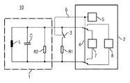
図1に示した受信回路10はNF送信周波数無線信号を受信する共振回路1と、後続の回路装置2を有する。共振回路は受信コイルLと、これに並列に接続されたコンデンサCを有する。受信コイルLは、空芯コイルまたはフェライトコアを有するコイルとして構成することができる。受信コイルのコイルワイヤおよび場合によりフェライトコアに起因して共振回路のQが温度経過するのを低減するために、抵抗R2を受信コイルLとコンデンサCに並列に接続することができる。抵抗R2の値は、共振回路の共振上昇が格段に変化しないような大きさに選択される。例えば125kHzで最適に受信するための高いQを可能にするために、2mHのインダクタンスを有する受信コイル、680pFのキャパシタンスを有するコンデンサC、および80kΩの抵抗R2を使用することができる。しかしもちろん、共振回路1の素子を別の値のものにし、他の共振周波数に対して構成することもできる。
The receiving
後続の回路装置2に供給される共振回路の出力信号は、並列接続された素子L、Cおよび場合によりR2を介して印加される。後続の回路2は、第1の回路7と第2の回路8を有する。 The output signal of the resonance circuit supplied to the subsequent circuit device 2 is applied via the elements L and C connected in parallel and optionally R2. The subsequent circuit 2 includes a first circuit 7 and a second circuit 8.
第1の回路7は、受信されたHF信号を通信技術的に処理するために必要なすべての回路素子を有する。受信回路を含む通信装置がさらにエネルギ蓄積器を充電するためのトランスポンダ機能を有しているならば、そのための切換回路も第1の回路7に含まれる。 The first circuit 7 has all the circuit elements necessary for processing the received HF signal in a communication technology. If the communication device including the receiving circuit further has a transponder function for charging the energy accumulator, a switching circuit therefor is also included in the first circuit 7.
第2の回路8は、NF信号の電界強度を表わす共振回路の出力信号を、受信コイルLの箇所で測定するために必要なすべての回路素子を有する。共振回路1のQが高い場合には測定公差も非常に大きくなるから、電界強度を十分に正確に検出するためには共振回路1を強く減衰しなければならない。このために図示の構成では、共振回路の出力端と並列に接続することのできる抵抗R1が用いられる。抵抗R1は共振回路1の素子に並列のアドミタンスを高め、共振回路の減衰に作用する。共振回路が減衰されると、振幅が低減され、並列共振回路1の共振曲線の幅が拡張される。 The second circuit 8 includes all circuit elements necessary for measuring the output signal of the resonance circuit representing the electric field strength of the NF signal at the receiving coil L. When the Q of the resonance circuit 1 is high, the measurement tolerance becomes very large. Therefore, in order to detect the electric field strength sufficiently accurately, the resonance circuit 1 must be strongly attenuated. For this reason, in the illustrated configuration, a resistor R1 that can be connected in parallel with the output terminal of the resonance circuit is used. The resistor R1 increases admittance parallel to the elements of the resonance circuit 1 and acts on attenuation of the resonance circuit. When the resonance circuit is attenuated, the amplitude is reduced and the width of the resonance curve of the parallel resonance circuit 1 is expanded.
後続の回路装置2はさらに回路制御部5を有する。この回路制御部は、スイッチ素子3と4の切換状態を制御する。2つのスイッチ素子3と4の切換状態は、共振回路の出力端が第1の回路7と接続されているときに抵抗R1が共振回路から分離され、共振回路の出力端が第2の回路8と接続されているときに第1の抵抗が共振回路に接続されるように相互に整合されている。言い替えるとスイッチ素子3は、スイッチ素子4が並列共振回路を回路7と接続するとき、図示の開放状態、すなわち線路遮断切換状態にあり、スイッチ素子4が並列共振回路を電界強度測定のために設けられた回路8と接続するとき、回路制御部はスイッチ素子3を閉成状態、すなわち線路接続切換状態に制御する。 The subsequent circuit device 2 further includes a circuit control unit 5. This circuit control unit controls the switching state of the switch elements 3 and 4. When the two switch elements 3 and 4 are switched, the resistor R1 is separated from the resonance circuit when the output terminal of the resonance circuit is connected to the first circuit 7 and the output terminal of the resonance circuit is the second circuit 8. Are connected to each other so that the first resistors are connected to the resonant circuit. In other words, when the switch element 4 connects the parallel resonant circuit to the circuit 7, the switch element 3 is in the open state shown in the figure, that is, the line cutoff switching state, and the switch element 4 is provided with the parallel resonant circuit for measuring the electric field strength. When the circuit 8 is connected, the circuit control unit controls the switch element 3 to the closed state, that is, the line connection switching state.
2つのスイッチ素子3と4の制御は回路制御部5によって、制御線路6を介して行われる。2つのスイッチ素子3と4の制御は同期して行うことも、非同期で行うこともできる。 The two switch elements 3 and 4 are controlled by the circuit control unit 5 via the control line 6. The control of the two switch elements 3 and 4 can be performed synchronously or asynchronously.
図1では、スイッチ素子が単純なスイッチとして構成されている。抵抗R1の両方の端子を共振回路の出力端から分離するダブルスイッチとしての構成も可能であり、とりわけ片側が閉じた抵抗の寄生作用が懸念される場合にはそうすべきである。共振回路1の端子の一方は通常、受信回路のアース電位と接続されているから、図1にダブルスイッチとして構成されたスイッチ素子4は単純な切換スイッチとしても実現できる。この場合、共振回路1のアース電位は常に回路7と8のアース電位と接続され、切換スイッチ4は共振回路1の他方の端子を選択的に、回路7または回路8のアースに接続されていない入力端と接続する。 In FIG. 1, the switch element is configured as a simple switch. A configuration as a double switch that separates both terminals of the resistor R1 from the output terminal of the resonance circuit is also possible, especially when there is a concern about the parasitic action of a resistor with one side closed. Since one of the terminals of the resonance circuit 1 is normally connected to the ground potential of the receiving circuit, the switch element 4 configured as a double switch in FIG. 1 can be realized as a simple changeover switch. In this case, the ground potential of the resonance circuit 1 is always connected to the ground potential of the circuits 7 and 8, and the changeover switch 4 does not selectively connect the other terminal of the resonance circuit 1 to the ground of the circuit 7 or the circuit 8. Connect to the input terminal.
スイッチ素子3と4は基本的に電気機械的コンポーネントとして構成することができる。しかし応答時間を短くし、コンタクトチャタリングを回避したい場合には、スイッチ素子が電子コンポーネントの形態に、有利にはトランジスタを使用して構成するのが有利である。 The switch elements 3 and 4 can basically be configured as electromechanical components. However, if it is desired to shorten the response time and avoid contact chattering, it is advantageous to configure the switching element in the form of an electronic component, preferably using a transistor.
図1は極端に簡素化して図示されており、本発明の理解に必要な素子だけが含まれていることを述べておく。受信回路の駆動またはその機能範囲の拡張に必要な別のコンポーネントを取り入れることは、分かりやすく図示するために省略した。それらのコンポーネントは存在しているものと仮定する。 It should be noted that FIG. 1 is illustrated in an extremely simplified manner and includes only elements necessary for an understanding of the present invention. Incorporation of other components necessary to drive the receiver circuit or extend its functional range has been omitted for the sake of clarity. Assume that these components exist.
受信されたNF信号(NFS、図2参照)の電界強度の測定は、エントリー構成体の2つの通信装置間の距離検出が必要な場合だけ行われる。通常、受信回路は基本状態にある。この基本状態では共振回路の出力端が、メッセージ通知のためと、場合により誘導性エネルギ伝達のトランスポンダ機能のために信号処理を行う第1の回路7と接続されている。これとは反対に、抵抗R1は共振回路1から電気的に分離されている。したがって共振回路1の減衰は非常に小さく、これによりメッセージ通知の際には高い信号Qが達成され、エネルギ伝達の際には高い効率が達成される。 The measurement of the electric field strength of the received NF signal (NFS, see FIG. 2) is performed only when it is necessary to detect the distance between the two communication devices of the entry structure. Usually, the receiving circuit is in a basic state. In this basic state, the output of the resonant circuit is connected to a first circuit 7 that performs signal processing for message notification and possibly for the transponder function of inductive energy transfer. On the contrary, the resistor R1 is electrically isolated from the resonance circuit 1. Therefore, the attenuation of the resonant circuit 1 is very small, so that a high signal Q is achieved during message notification and a high efficiency is achieved during energy transfer.
測定状態では抵抗R1が共振回路1と接続され、共振回路の出力端は、受信電界強度測定のための回路を含む回路8と接続される。共振回路1を抵抗R1により付加的に減衰することにより、共振回路1のQが低減され、これにより受信電界強度の測定精度が向上する。減衰が高められたときに出力信号の振幅が小さくなることは、比較的に高い増幅によって補償することができる。測定は一時的に短い時間だけ行われるから、増幅と結び付いた電流消費の増大は受信回路の全体エネルギ消費の増大にはほとんど至らない。これにより全体として、良好な受信品質、高いエネルギ伝達効率、電界強度検出における狭い測定公差を備えた低エネルギ消費型受信回路10が実現される。
In the measurement state, the resistor R1 is connected to the resonance circuit 1, and the output terminal of the resonance circuit is connected to a circuit 8 including a circuit for measuring the received electric field strength. By additionally attenuating the resonance circuit 1 with the resistor R1, the Q of the resonance circuit 1 is reduced, thereby improving the measurement accuracy of the received electric field strength. A reduction in the amplitude of the output signal when the attenuation is increased can be compensated by a relatively high amplification. Since the measurement is temporarily performed for a short period of time, the increase in current consumption associated with amplification hardly leads to an increase in the overall energy consumption of the receiving circuit. As a result, a low energy consumption
本発明の詳細を、並列回路に構成された受信回路を参照して説明したが、本発明はこれに限定されるものではないことを述べておく。受信コイルとコンデンサが直列回路に構成された受信回路、または1つまたは複数の受信コイルと1つまたは複数のコンデンサおよび抵抗による直列回路/並列回路の組合せを備える受信回路も可能である。 Although the details of the present invention have been described with reference to a receiving circuit configured in a parallel circuit, it should be noted that the present invention is not limited to this. A receiving circuit in which the receiving coil and the capacitor are configured in a series circuit, or a combination of a series circuit / parallel circuit with one or more receiving coils and one or more capacitors and resistors is also possible.
すでに上に述べたように、受信回路10は例えば第2の通信装置KE2に組み込むことができる。このようにして従来技術に対して改善された、車両FZ用のエントリー構成体が実現される。
As already mentioned above, the receiving
1 共振回路
2 後続の回路装置
3 スイッチ素子
4 切換スイッチ装置
5 回路制御部
6 制御線路
7 信号処理/充電装置
8 測定装置
10 受信回路
L 受信コイル
C コンデンサ
R1 第1の抵抗
R2 第2の抵抗
IG 識別発生器
FZ 自動車
HFS 高周波信号
NFS 低周波信号
CO 認証コード
KE1 車両側(第1の)通信装置
KE2 識別発生器側(第2の)通信装置
TS ドア錠/保安装置
DESCRIPTION OF SYMBOLS 1 Resonant circuit 2 Subsequent circuit apparatus 3 Switch element 4 Changeover switch apparatus 5 Circuit control part 6 Control line 7 Signal processing / charging apparatus 8
Claims (11)
該受信回路は、磁気誘導を電流に変換するための受信コイル(L)とコンデンサ(C)とを含む共振回路を備える形式の受信回路において、
前記受信回路(10)はさらに第1の抵抗(R1)と、該第1の抵抗(R1)を前記共振回路(1)に接続および分離するように制御可能なスイッチ素子(3)とを有する、ことを特徴とする受信回路。 A receiving circuit for a communication device of an entry structure, wherein the receiving circuit includes a resonance circuit including a receiving coil (L) and a capacitor (C) for converting magnetic induction into a current,
The receiver circuit (10) further includes a first resistor (R1) and a switch element (3) that can be controlled to connect and disconnect the first resistor (R1) from the resonant circuit (1). A receiving circuit characterized by that.
前記受信コイル(L)とコンデンサ(C)は並列回路に配置されている、ことを特徴とする受信回路。 The receiving circuit according to claim 1,
The receiving circuit, wherein the receiving coil (L) and the capacitor (C) are arranged in a parallel circuit.
前記受信コイル(L)とコンデンサ(C)は直列に接続されて配置されている、ことを特徴とする受信回路。 The receiving circuit according to claim 1 or 2,
The receiving circuit, wherein the receiving coil (L) and the capacitor (C) are connected in series.
前記スイッチ素子(3)は、共振回路(1)と第1の抵抗(R1)を並列に接続する第1の切換状態を有する、ことを特徴とする受信回路。 The receiving circuit according to any one of claims 1 to 3,
The switching element (3) has a first switching state in which the resonance circuit (1) and the first resistor (R1) are connected in parallel.
前記スイッチ素子(3)は、共振回路(1)と第1の抵抗(R1)を直列に接続する第1の切換状態を有する、ことを特徴とする受信回路。 The receiving circuit according to any one of claims 1 to 3,
The switch element (3) has a first switching state in which the resonance circuit (1) and the first resistor (R1) are connected in series.
前記スイッチ素子(4)は、共振回路(1)と第1の抵抗(R1)との電気接続を分離する第2の切換状態を有する、ことを特徴とする受信回路。 The receiving circuit according to any one of claims 1 to 5,
The switch element (4) has a second switching state for separating an electrical connection between the resonance circuit (1) and the first resistor (R1).
前記共振回路(1)は別の抵抗(R2)を有し、該別の抵抗は受信コイル(L)および/またはコンデンサ(C)に並列または直列に接続されている、ことを特徴とする受信回路。 The receiving circuit according to any one of claims 1 to 6,
The resonance circuit (1) has another resistor (R2), and the other resistor is connected in parallel or in series to the receiving coil (L) and / or the capacitor (C). circuit.
請求項1から7までのいずれか1項記載の受信回路(10)を備え、誘導性周波数領域の問い合わせ信号を受信し、さらに処理する第2の通信装置(KE2)とを有するエントリー構成体。 A first communication device (KE1) for transmitting at least one inquiry signal (NFS) in the inductive frequency domain;
8. An entry structure comprising a receiving circuit (10) according to any one of claims 1 to 7, comprising a second communication device (KE2) for receiving and further processing an inductive frequency domain inquiry signal.
第1のステップで、共振回路(1)の接続が第1の回路(7)から第2の回路(8)に変化する場合に、共振回路(1)を第1の抵抗と電気的に接続し、
第2のステップで共振回路の接続が第2の回路(8)から第1の回路(7)に変化する場合に、第1の抵抗を共振回路から電気的に分離する方法。 A method of changing the Q of a resonant circuit,
When the connection of the resonance circuit (1) changes from the first circuit (7) to the second circuit (8) in the first step, the resonance circuit (1) is electrically connected to the first resistor. And
A method of electrically separating the first resistor from the resonant circuit when the connection of the resonant circuit changes from the second circuit (8) to the first circuit (7) in the second step.
共振回路(1)と第1の抵抗(R1)との電気接続および電気分離は、電気接続のための2つの線路の一方でだけ行われる、ことを特徴とする方法。 The method of claim 10, wherein:
A method characterized in that the electrical connection and electrical isolation between the resonant circuit (1) and the first resistor (R1) is made only on one of the two lines for electrical connection.
Applications Claiming Priority (3)
| Application Number | Priority Date | Filing Date | Title |
|---|---|---|---|
| DE102007004814A DE102007004814B4 (en) | 2007-01-31 | 2007-01-31 | Quality adjustment of a receiving circuit |
| DE102007004814.0 | 2007-01-31 | ||
| PCT/EP2008/050419 WO2008092741A1 (en) | 2007-01-31 | 2008-01-16 | Quality adjustment of a receiving circuit |
Publications (2)
| Publication Number | Publication Date |
|---|---|
| JP2010517455A true JP2010517455A (en) | 2010-05-20 |
| JP4914501B2 JP4914501B2 (en) | 2012-04-11 |
Family
ID=39154135
Family Applications (1)
| Application Number | Title | Priority Date | Filing Date |
|---|---|---|---|
| JP2009547628A Active JP4914501B2 (en) | 2007-01-31 | 2008-01-16 | Reception circuit and method for changing Q of resonance circuit |
Country Status (7)
| Country | Link |
|---|---|
| US (1) | US9148189B2 (en) |
| EP (1) | EP2115704B1 (en) |
| JP (1) | JP4914501B2 (en) |
| CN (1) | CN101657843B (en) |
| AT (1) | ATE479171T1 (en) |
| DE (2) | DE102007004814B4 (en) |
| WO (1) | WO2008092741A1 (en) |
Families Citing this family (7)
| Publication number | Priority date | Publication date | Assignee | Title |
|---|---|---|---|---|
| FR2965082B1 (en) | 2010-09-21 | 2012-09-28 | Inside Contactless | METHOD AND DEVICE FOR INDUCTIVE COUPLING ACTIVATED LOAD MODULATION |
| DE102011117978A1 (en) | 2010-11-11 | 2012-05-16 | Marquardt Gmbh | Locking system, in particular for a motor vehicle |
| FR3007875B1 (en) * | 2013-06-28 | 2015-07-17 | Continental Automotive France | METHOD FOR PROTECTING A FREE ACCESS AND / OR START SYSTEM OF A VEHICLE BY MODIFYING THE SIGNAL RECEPTION SPEED |
| CN104753183B (en) * | 2013-12-30 | 2018-05-04 | 华为技术有限公司 | A kind of circuit control method, device and a kind of receiving circuit |
| DE102014222603B3 (en) * | 2014-11-05 | 2015-12-24 | Continental Automotive Gmbh | Driver circuit for an inductance and active transmitting device with a driver circuit |
| CN109728655A (en) * | 2019-03-01 | 2019-05-07 | 中国矿业大学(北京) | Variable topology magnetically coupled resonant wireless power transfer system and method |
| CN111815962A (en) * | 2020-07-08 | 2020-10-23 | 支付宝(杭州)信息技术有限公司 | Vehicle identity identification method and device, master device and slave device |
Citations (7)
| Publication number | Priority date | Publication date | Assignee | Title |
|---|---|---|---|---|
| US5616966A (en) * | 1994-11-07 | 1997-04-01 | Siemens Aktiengesellschaft | Anti-theft system for a motor vehicle |
| US5804888A (en) * | 1994-08-26 | 1998-09-08 | Siemens Aktiengesellschaft | Anti-theft system for a motor vehicle |
| WO2001024108A1 (en) * | 1999-09-28 | 2001-04-05 | Fujitsu Limited | Noncontact ic card capable of inhibiting data transmission |
| JP2002064402A (en) * | 2000-08-23 | 2002-02-28 | Nippon Telegr & Teleph Corp <Ntt> | Non-contact response device |
| JP2002334310A (en) * | 2001-05-10 | 2002-11-22 | Hitachi Ltd | Non-contact IC card and method of adjusting antenna resonance circuit thereof |
| WO2006052867A1 (en) * | 2004-11-08 | 2006-05-18 | Checkpoint Systems, Inc. | System and method for detecting eas/rfid tags using step listen |
| JP2007500461A (en) * | 2003-07-30 | 2007-01-11 | ギーゼッケ ウント デフリエント ゲーエムベーハー | A communication device that establishes a data connection between intelligent devices |
Family Cites Families (23)
| Publication number | Priority date | Publication date | Assignee | Title |
|---|---|---|---|---|
| US3135919A (en) * | 1960-08-26 | 1964-06-02 | Collins Radio Co | Tone frequency control means for kinematically filtered systems |
| US5025492A (en) * | 1990-04-11 | 1991-06-18 | Texas Instruments Deutschland Gmbh | Damping circuit for the antenna resonance circuit of a radio transmitter-receiver |
| US5287112A (en) * | 1993-04-14 | 1994-02-15 | Texas Instruments Incorporated | High speed read/write AVI system |
| DE4323530A1 (en) * | 1993-07-14 | 1995-01-19 | Philips Patentverwaltung | Data exchange arrangement |
| US5541604A (en) * | 1993-09-03 | 1996-07-30 | Texas Instruments Deutschland Gmbh | Transponders, Interrogators, systems and methods for elimination of interrogator synchronization requirement |
| JPH0844833A (en) * | 1994-08-03 | 1996-02-16 | Mitsubishi Denki Semiconductor Software Kk | Non-contact IC card reader / writer and non-contact IC card reader / writer system |
| DE4438287C1 (en) * | 1994-10-26 | 1996-05-09 | Siemens Ag | System for contactless energy and data transmission |
| JP3634030B2 (en) * | 1995-10-25 | 2005-03-30 | 株式会社東海理化電機製作所 | Transmission / reception system |
| NL1001770C2 (en) * | 1995-11-29 | 1997-05-30 | Nedap Nv | Deactivatable article monitoring label with data carrier function. |
| US6167236A (en) | 1996-01-31 | 2000-12-26 | Texas Instruments Deutschland, Gmbh | Damping modulation circuit for a full-duplex transponder |
| AUPO055296A0 (en) * | 1996-06-19 | 1996-07-11 | Integrated Silicon Design Pty Ltd | Enhanced range transponder system |
| DE19642568A1 (en) | 1996-10-15 | 1998-04-23 | Siemens Ag | Data transmission circuit with a station and with a response circuit |
| FR2792130B1 (en) * | 1999-04-07 | 2001-11-16 | St Microelectronics Sa | ELECTROMAGNETIC TRANSPONDER WITH VERY CLOSE COUPLING OPERATION |
| DE19927319A1 (en) * | 1999-06-15 | 2000-12-21 | Mannesmann Vdo Ag | Method for determining the distance between two devices of an identification system |
| FR2811108B1 (en) * | 2000-06-29 | 2002-09-27 | A S K | NON-CONTACT PERIPHERAL DISPLAY DEVICE FOR NON-CONTACT PORTABLE OBJECT |
| FR2831305B1 (en) * | 2001-10-23 | 2004-01-30 | Inside Technologies | CONTACTLESS INTEGRATED CIRCUIT COMPRISING AUTOMATIC FRAME IDENTIFICATION MEANS |
| CN1333367C (en) * | 2001-11-16 | 2007-08-22 | 皇家飞利浦电子股份有限公司 | Data carrier for transmitting data with different transmission parameters |
| JP3565217B2 (en) * | 2002-10-29 | 2004-09-15 | オムロン株式会社 | Article management system, non-contact electronic tag, and article management program |
| JP4104502B2 (en) | 2003-07-25 | 2008-06-18 | アルプス電気株式会社 | Passive keyless entry device |
| TWI220338B (en) * | 2003-08-15 | 2004-08-11 | Delta Electronics Inc | Front end module for mobile telecommunication system |
| US20050237160A1 (en) | 2004-04-23 | 2005-10-27 | Microchip Technology Incorporated | Reducing false wake-up in a low frequency transponder |
| DE102006031044B4 (en) * | 2005-07-06 | 2017-02-02 | Denso Corporation | Wheel identification device and tire inflation pressure detection device with a wheel identification function |
| DE102006007261A1 (en) * | 2006-02-10 | 2007-08-23 | Atmel Germany Gmbh | Transponder and method for wireless data transmission |
-
2007
- 2007-01-31 DE DE102007004814A patent/DE102007004814B4/en not_active Expired - Fee Related
-
2008
- 2008-01-16 DE DE502008001203T patent/DE502008001203D1/en active Active
- 2008-01-16 CN CN2008800092862A patent/CN101657843B/en active Active
- 2008-01-16 AT AT08701511T patent/ATE479171T1/en active
- 2008-01-16 EP EP08701511A patent/EP2115704B1/en active Active
- 2008-01-16 JP JP2009547628A patent/JP4914501B2/en active Active
- 2008-01-16 WO PCT/EP2008/050419 patent/WO2008092741A1/en not_active Ceased
- 2008-01-16 US US12/525,118 patent/US9148189B2/en active Active
Patent Citations (7)
| Publication number | Priority date | Publication date | Assignee | Title |
|---|---|---|---|---|
| US5804888A (en) * | 1994-08-26 | 1998-09-08 | Siemens Aktiengesellschaft | Anti-theft system for a motor vehicle |
| US5616966A (en) * | 1994-11-07 | 1997-04-01 | Siemens Aktiengesellschaft | Anti-theft system for a motor vehicle |
| WO2001024108A1 (en) * | 1999-09-28 | 2001-04-05 | Fujitsu Limited | Noncontact ic card capable of inhibiting data transmission |
| JP2002064402A (en) * | 2000-08-23 | 2002-02-28 | Nippon Telegr & Teleph Corp <Ntt> | Non-contact response device |
| JP2002334310A (en) * | 2001-05-10 | 2002-11-22 | Hitachi Ltd | Non-contact IC card and method of adjusting antenna resonance circuit thereof |
| JP2007500461A (en) * | 2003-07-30 | 2007-01-11 | ギーゼッケ ウント デフリエント ゲーエムベーハー | A communication device that establishes a data connection between intelligent devices |
| WO2006052867A1 (en) * | 2004-11-08 | 2006-05-18 | Checkpoint Systems, Inc. | System and method for detecting eas/rfid tags using step listen |
Also Published As
| Publication number | Publication date |
|---|---|
| DE102007004814A1 (en) | 2008-08-14 |
| CN101657843B (en) | 2012-08-15 |
| EP2115704A1 (en) | 2009-11-11 |
| JP4914501B2 (en) | 2012-04-11 |
| US9148189B2 (en) | 2015-09-29 |
| CN101657843A (en) | 2010-02-24 |
| DE102007004814B4 (en) | 2013-06-06 |
| US20100127820A1 (en) | 2010-05-27 |
| WO2008092741A1 (en) | 2008-08-07 |
| ATE479171T1 (en) | 2010-09-15 |
| DE502008001203D1 (en) | 2010-10-07 |
| EP2115704B1 (en) | 2010-08-25 |
Similar Documents
| Publication | Publication Date | Title |
|---|---|---|
| JP4914501B2 (en) | Reception circuit and method for changing Q of resonance circuit | |
| US9124302B2 (en) | Carrier frequency variation for device detection in near-field communications | |
| JP5491331B2 (en) | Communication mode setting device | |
| KR102048427B1 (en) | Detection and near-field communication device | |
| US8977197B2 (en) | Circuit tuning for device detection in near-field communications | |
| CN119892260B (en) | NFC electric field detection system, method and NFC device | |
| JP2011142769A (en) | Method and device for transmitting magnetic resonance power | |
| JP5888825B2 (en) | Theft inspection device and theft inspection method | |
| US20150340876A1 (en) | Pru short beacon detection | |
| US20110287732A1 (en) | Wireless communication apparatus | |
| KR102276504B1 (en) | Near Field Communication and Approach Detection Device | |
| KR102834690B1 (en) | Access System | |
| JP5548075B2 (en) | Communication output setting device | |
| JP5416065B2 (en) | Communication mode setting device | |
| WO2016063717A1 (en) | Keyless entry device | |
| CN112368947B (en) | Vehicle device for contactless data transmission | |
| US20170133885A1 (en) | Notch filter utilized for near field communication and wireless power transfer dual mode antennas | |
| US20240353240A1 (en) | Device for detecting an approach | |
| CN216750296U (en) | Near field communication antenna and near field communication intelligence lock | |
| JP2013102642A (en) | Non-contact charger | |
| HK40112154A (en) | Nfc electric field detection system and method and nfc equipment | |
| CN113162582B (en) | Authentication reader for opening parts of motor vehicles | |
| KR20190054868A (en) | Wireless power transmiting apparatus having data communication function | |
| CN117836499A (en) | Proximity detection device | |
| JP2019017164A (en) | Power transmission device |
Legal Events
| Date | Code | Title | Description |
|---|---|---|---|
| RD04 | Notification of resignation of power of attorney |
Free format text: JAPANESE INTERMEDIATE CODE: A7424 Effective date: 20101228 |
|
| A131 | Notification of reasons for refusal |
Free format text: JAPANESE INTERMEDIATE CODE: A131 Effective date: 20110323 |
|
| A601 | Written request for extension of time |
Free format text: JAPANESE INTERMEDIATE CODE: A601 Effective date: 20110621 |
|
| A602 | Written permission of extension of time |
Free format text: JAPANESE INTERMEDIATE CODE: A602 Effective date: 20110628 |
|
| A521 | Request for written amendment filed |
Free format text: JAPANESE INTERMEDIATE CODE: A523 Effective date: 20110722 |
|
| A131 | Notification of reasons for refusal |
Free format text: JAPANESE INTERMEDIATE CODE: A131 Effective date: 20110902 |
|
| A521 | Request for written amendment filed |
Free format text: JAPANESE INTERMEDIATE CODE: A523 Effective date: 20111124 |
|
| TRDD | Decision of grant or rejection written | ||
| A01 | Written decision to grant a patent or to grant a registration (utility model) |
Free format text: JAPANESE INTERMEDIATE CODE: A01 Effective date: 20111222 |
|
| A01 | Written decision to grant a patent or to grant a registration (utility model) |
Free format text: JAPANESE INTERMEDIATE CODE: A01 |
|
| A61 | First payment of annual fees (during grant procedure) |
Free format text: JAPANESE INTERMEDIATE CODE: A61 Effective date: 20120120 |
|
| R150 | Certificate of patent or registration of utility model |
Ref document number: 4914501 Country of ref document: JP Free format text: JAPANESE INTERMEDIATE CODE: R150 Free format text: JAPANESE INTERMEDIATE CODE: R150 |
|
| FPAY | Renewal fee payment (event date is renewal date of database) |
Free format text: PAYMENT UNTIL: 20150127 Year of fee payment: 3 |
|
| R250 | Receipt of annual fees |
Free format text: JAPANESE INTERMEDIATE CODE: R250 |
|
| R250 | Receipt of annual fees |
Free format text: JAPANESE INTERMEDIATE CODE: R250 |
|
| R250 | Receipt of annual fees |
Free format text: JAPANESE INTERMEDIATE CODE: R250 |
|
| R250 | Receipt of annual fees |
Free format text: JAPANESE INTERMEDIATE CODE: R250 |
|
| R250 | Receipt of annual fees |
Free format text: JAPANESE INTERMEDIATE CODE: R250 |
|
| R250 | Receipt of annual fees |
Free format text: JAPANESE INTERMEDIATE CODE: R250 |
|
| R250 | Receipt of annual fees |
Free format text: JAPANESE INTERMEDIATE CODE: R250 |
|
| R250 | Receipt of annual fees |
Free format text: JAPANESE INTERMEDIATE CODE: R250 |
|
| R250 | Receipt of annual fees |
Free format text: JAPANESE INTERMEDIATE CODE: R250 |
|
| S111 | Request for change of ownership or part of ownership |
Free format text: JAPANESE INTERMEDIATE CODE: R313113 |
|
| S631 | Written request for registration of reclamation of domicile |
Free format text: JAPANESE INTERMEDIATE CODE: R313631 |
|
| R350 | Written notification of registration of transfer |
Free format text: JAPANESE INTERMEDIATE CODE: R350 |
|
| R250 | Receipt of annual fees |
Free format text: JAPANESE INTERMEDIATE CODE: R250 |
|
| R250 | Receipt of annual fees |
Free format text: JAPANESE INTERMEDIATE CODE: R250 |
|
| R250 | Receipt of annual fees |
Free format text: JAPANESE INTERMEDIATE CODE: R250 |