JP2010281988A - Optical module and optical waveguide structure - Google Patents
Optical module and optical waveguide structure Download PDFInfo
- Publication number
- JP2010281988A JP2010281988A JP2009134699A JP2009134699A JP2010281988A JP 2010281988 A JP2010281988 A JP 2010281988A JP 2009134699 A JP2009134699 A JP 2009134699A JP 2009134699 A JP2009134699 A JP 2009134699A JP 2010281988 A JP2010281988 A JP 2010281988A
- Authority
- JP
- Japan
- Prior art keywords
- optical waveguide
- optical
- waveguide
- light
- emitting element
- Prior art date
- Legal status (The legal status is an assumption and is not a legal conclusion. Google has not performed a legal analysis and makes no representation as to the accuracy of the status listed.)
- Granted
Links
Images


Abstract
Description
本発明は、例えば光通信などに用いる光モジュール及び光導波路構造体に関する。 The present invention relates to an optical module and an optical waveguide structure used for optical communication, for example.
近年、例えば面発光レーザ(発光素子)やフォトダイオード(フォトディテクタ;受光素子)などの面型光素子を備える多チャンネル光トランシーバ(例えば波長多重多チャンネル光トランシーバ)の開発が進められている。
例えば多チャンネル光トランシーバなどの光モジュールにおいて、面発光レーザやフォトダイオードなどの面型光素子を使用する場合、面型光素子の光入射面(受光面)又は光出射面(発光面)は実装基板に対して平行になる。このため、実装基板に対して垂直に光を入射又は出射させることになる。
In recent years, development of multi-channel optical transceivers (for example, wavelength division multi-channel optical transceivers) including surface optical elements such as surface-emitting lasers (light-emitting elements) and photodiodes (photo-detectors; light-receiving elements) has been underway.
For example, when using a surface optical device such as a surface emitting laser or a photodiode in an optical module such as a multi-channel optical transceiver, the light incident surface (light receiving surface) or light emitting surface (light emitting surface) of the surface optical device is mounted. Parallel to the substrate. For this reason, light is incident or emitted perpendicularly to the mounting substrate.
一方、このような光モジュールにおいては、小型化、薄型化を図ることが必要である。
小型化、薄型化を図るためには、光ファイバ(光ファイバアレイ)を実装基板に対して平行に配置するのが望ましい。この場合、光ファイバの端面と面型光素子の光入射面又は光出射面とは略直角の位置関係になる。
このため、基板上に実装された面型光素子の光入射面又は光出射面に対して垂直に入射又は出射する光の経路(光路)を略90度曲げて、光ファイバアレイと面型光素子とを光学的に接続することが必要になる。
On the other hand, it is necessary to reduce the size and thickness of such an optical module.
In order to reduce the size and thickness, it is desirable to arrange the optical fiber (optical fiber array) in parallel with the mounting substrate. In this case, the end face of the optical fiber and the light incident surface or light emitting surface of the surface optical element are in a substantially right-angle positional relationship.
For this reason, the optical fiber array and the surface light are bent by approximately 90 degrees of the light path (optical path) incident or emitted perpendicular to the light incident surface or the light emitting surface of the surface optical element mounted on the substrate. It is necessary to optically connect the element.
そこで、例えば光トランシーバなどの装置内の狭いスペースで光の経路を急峻に曲げるために、略直角の曲面上に光導波路(曲線光導波路)を有する光導波路構造体を用い、面型光素子に対して入射又は出射する光を、曲面に沿って導いて、光ファイバアレイに結合させる技術がある(第1の技術)。
このような光導波路構造体は、曲面上に予め形成した細溝内に、液状コア材料を滴下し、その上にフィルムを貼り付け、シリコンゴムのような柔らかい素材を用いて一定の圧力で押さえ付けることによって液状コア材料を薄く延ばし、紫外線照射によって硬化させることによって製造される。
Therefore, in order to sharply bend the light path in a narrow space in an apparatus such as an optical transceiver, for example, an optical waveguide structure having an optical waveguide (curved optical waveguide) on a substantially perpendicular curved surface is used. On the other hand, there is a technique in which light incident or emitted is guided along a curved surface and coupled to an optical fiber array (first technique).
In such an optical waveguide structure, a liquid core material is dropped into a narrow groove formed in advance on a curved surface, a film is pasted thereon, and a soft material such as silicon rubber is used and pressed with a certain pressure. It is manufactured by thinly extending the liquid core material by applying and curing it by ultraviolet irradiation.
また、光導波路構造体の表裏両面に曲線光導波路を設け、一面側の曲線光導波路によって受光素子と光ファイバとを接続し、他面側の曲線光導波路によって発光素子と光ファイバとを接続するようにした技術もある(第2の技術)。
また、一本の光ファイバでの双方向通信を可能にするものとして、一本の光ファイバのコア領域に対向する位置に、発光素子に接続される送信光用直線導波路と、受光素子に接続される受信光用直線導波路とを別々に設ける技術もある(第3の技術)。
Also, curved optical waveguides are provided on both the front and back surfaces of the optical waveguide structure, the light receiving element and the optical fiber are connected by the curved optical waveguide on one side, and the light emitting element and the optical fiber are connected by the curved optical waveguide on the other side. There is also a technique as described above (second technique).
In addition, in order to enable two-way communication with a single optical fiber, a transmission light linear waveguide connected to the light emitting element at a position facing the core region of the single optical fiber, and a light receiving element. There is also a technique of separately providing a linear waveguide for received light to be connected (third technique).
ところで、上述の第1の技術においてチャンネル数を増やして多チャンネル化を図る場合、例えば上述の第2の技術のように、光導波路構造体の表裏両面に曲線光導波路を設けることが考えられる。
しかしながら、上述の第2の技術のように、光導波路構造体の表裏両面に曲線光導波路を設ける場合、チャンネル数の増加にしたがって、光ファイバの本数が増え、光ファイバの配線スペースが増大してしまうことになる。なお、この点は、平面上に曲線光導波路を有する光導波路構造体においても同様である。
By the way, when the number of channels is increased in the first technique described above to increase the number of channels, it is conceivable to provide curved optical waveguides on both the front and back surfaces of the optical waveguide structure, for example, as in the second technique described above.
However, when the curved optical waveguides are provided on both the front and back surfaces of the optical waveguide structure as in the second technique described above, the number of optical fibers increases as the number of channels increases, and the optical fiber wiring space increases. Will end up. This also applies to an optical waveguide structure having a curved optical waveguide on a plane.
この場合、上述の第3の技術のように、一本の光ファイバで双方向通信を行なうようにすることが考えられる。
しかしながら、上述の第3の技術では、一本の光ファイバのコア領域に対向する位置に送信光用直線導波路と受信光用直線導波路とを別々に設けているため、光ファイバからの光が受信光用導波路に結合せずに漏れてしまい、損失が大きい。
In this case, it is conceivable to perform bidirectional communication using a single optical fiber as in the third technique described above.
However, in the third technique described above, the transmission light linear waveguide and the reception light linear waveguide are separately provided at positions facing the core region of one optical fiber. Leaks without being coupled to the received light waveguide, resulting in a large loss.
そこで、光導波路構造体に接続される光ファイバの本数を増やすことなく、チャンネル数を増加させるために双方向通信を行なうようにし、この場合に、一本の光ファイバと受光素子及び発光素子とを光学的に接続する際の損失を低減したい。 Therefore, bidirectional communication is performed to increase the number of channels without increasing the number of optical fibers connected to the optical waveguide structure. In this case, one optical fiber, a light receiving element, and a light emitting element I want to reduce the loss when I connect the optically.
このため、本光モジュールは、光ファイバと受光素子及び発光素子とを光学的に接続する曲線光導波路を有する光導波路構造体を備え、曲線光導波路は、受光素子及び発光素子に接続される側の端面へ向けて幅又は厚さがテーパ状に大きくなる導波路コアを有し、導波路コアの外側部分に光学的に接続された受光素子と、導波路コアの内側部分に光学的に接続された発光素子とを備えることを要件とする。 Therefore, the optical module includes an optical waveguide structure having a curved optical waveguide that optically connects the optical fiber, the light receiving element, and the light emitting element, and the curved optical waveguide is connected to the light receiving element and the light emitting element. A light receiving element optically connected to the outer part of the waveguide core and optically connected to the inner part of the waveguide core. It is necessary to provide a light emitting element that has been manufactured.
本光導波路構造体は、光ファイバと受光素子及び発光素子とを光学的に接続する曲線光導波路を備え、曲線光導波路は、受光素子及び発光素子に接続される側の端面へ向けて幅又は厚さがテーパ状に大きくなる導波路コアを有し、導波路コアの外側部分から出射される光を受光素子へ導く第1レンズ又は第1ミラーと、発光素子から出射される光を導波路コアの内側部分へ導く第2レンズ又は第2ミラーとを備えることを要件とする。 The optical waveguide structure includes a curved optical waveguide that optically connects an optical fiber, a light receiving element, and a light emitting element, and the curved optical waveguide has a width or a width toward an end face on a side connected to the light receiving element and the light emitting element. A waveguide core having a thickness that increases in a tapered shape; a first lens or a first mirror that guides light emitted from an outer portion of the waveguide core to the light receiving element; and light emitted from the light emitting element. It is a requirement to include a second lens or a second mirror that leads to the inner part of the core.
したがって、本光モジュール及び光導波路構造体によれば、双方向通信を行なうため、光導波路構造体に接続される光ファイバの本数を増やすことなく、チャンネル数を増加させることができるという利点がある。また、双方向通信を行なう場合に、一本の光ファイバと受光素子及び発光素子とを光学的に接続する際の損失を低減することができるという利点もある。 Therefore, according to the present optical module and the optical waveguide structure, since bidirectional communication is performed, there is an advantage that the number of channels can be increased without increasing the number of optical fibers connected to the optical waveguide structure. . In addition, when bidirectional communication is performed, there is an advantage that loss when optically connecting one optical fiber, a light receiving element, and a light emitting element can be reduced.
以下、図面により、本実施形態にかかる光モジュール及び光導波路構造体について説明する。
[第1実施形態]
第1実施形態にかかる光モジュール及び光導波路構造体について、図1を参照しながら説明する。
Hereinafter, the optical module and the optical waveguide structure according to the present embodiment will be described with reference to the drawings.
[First Embodiment]
The optical module and the optical waveguide structure according to the first embodiment will be described with reference to FIG.
本実施形態にかかる光モジュールは、例えば、入力された電気信号を光信号に変換し、光ファイバを介して送信する機能(光送信機)と、光ファイバを介して入力された光信号を電気信号に変換して受信する機能(光受信機)とを備える光トランシーバである。
本光モジュールは、図1に示すように、表面に入射面(受光面)を有する面型受光素子(面型光素子)1と、表面に出射面(発光面)を有する面型発光素子(面型光素子)2と、光の経路を急峻に曲げるために曲面上に光導波路(曲線光導波路)3を有する光導波路構造体4とを備える。つまり、これらの面型受光素子1、面型発光素子2、光導波路構造体3を、図示しないプリント基板(回路基板)上に実装することで、光モジュール5が形成される。
The optical module according to the present embodiment, for example, converts an input electrical signal into an optical signal and transmits the optical signal via an optical fiber (optical transmitter), and electrically converts the optical signal input via the optical fiber. An optical transceiver having a function (optical receiver) for converting into a signal and receiving the signal.
As shown in FIG. 1, the present optical module includes a surface light-receiving element (surface-type optical element) 1 having an incident surface (light-receiving surface) on the surface and a surface light-emitting element (surface-emitting element) having an emission surface (light-emitting surface) on the surface. A planar optical element) 2 and an optical waveguide structure 4 having an optical waveguide (curved optical waveguide) 3 on a curved surface in order to sharply bend the light path. That is, the
なお、図1では、一の光モジュール5(面型受光素子1、面型発光素子2、光導波路構造体4を含む)と、他の光モジュール5A(面型受光素子1、面型発光素子2、光導波路構造体4を含む)とを、光ファイバ10によって接続した光通信システムを示している。
ここで、面型受光素子1は、フォトダイオード(フォトディテクタ;PD;Photo detector)である。
In FIG. 1, one optical module 5 (including the surface
Here, the surface light-receiving
面型発光素子2は、面発光レーザ[VCSEL(Vertical-Cavity Surface−Emitting Laser)]である。
光導波路構造体4は、曲線状の導波路コア6内を光が伝播するように形成された曲線光導波路部品(例えばポリマを主材料とするポリマ光導波路)である。
ここでは、光導波路構造体4は、図1に示すように、曲面上に形成された溝7を有するクラッド構造体8(下部クラッド)と、溝7に形成された導波路コア6と、導波路コア6を覆うクラッドフィルム9(上部クラッド)とを有する。
The surface
The optical waveguide structure 4 is a curved optical waveguide component (for example, a polymer optical waveguide whose main material is a polymer) formed so that light propagates in the curved waveguide core 6.
Here, as shown in FIG. 1, the optical waveguide structure 4 includes a clad structure 8 (lower clad) having a
具体的には、クラッド構造体8は、図1に示すように、構造体表面の曲面上に、曲面の一端から他端まで延びる溝7(曲線状の溝;導波路用溝;細溝)を有する曲面構造体である。
ここでは、クラッド構造体8は、透明なクラッド材料からなる透明部材によって形成された透明構造体であって、屈折率n1を有する。例えばオレフィン系ポリマ(例えばポリオレフィン)を用いたモールド成型体(樹脂成型体)である。
Specifically, as shown in FIG. 1, the
Here, the
導波路コア6は、図1に示すように、クラッド構造体8の曲面表層部に形成された溝7を透明なコア材料で埋め込むことによって形成されている。このため、導波路コア6は、クラッド構造体8の曲面に沿って曲線状に形成されている。この導波路コア6は、クラッド構造体8の屈折率n1よりも大きい屈折率n2を有する(n2>n1)。なお、本実施形態では、導波路コア6を、液状コア材料(液状接着剤)を塗布し、硬化させて形成しているため、硬化後の屈折率がn2になる材料(屈折率がn2の透明固体)を用いる。
As shown in FIG. 1, the waveguide core 6 is formed by embedding a
クラッドフィルム9は、図1に示すように、クラッド構造体8の曲面上の溝7に形成された導波路コア6を覆うようにラミネートされている。このクラッドフィルム9は、導波路コア6の屈折率n2よりも小さい屈折率n3を有する(n3<n2)。
特に、本実施形態では、図1に示すように、曲線光導波路3の導波路コア6は、面型受光素子1及び面型発光素子2に接続される側の端面6Aへ向けて厚さがテーパ状に厚くなっている。
As shown in FIG. 1, the clad film 9 is laminated so as to cover the waveguide core 6 formed in the
In particular, in the present embodiment, as shown in FIG. 1, the waveguide core 6 of the curved
具体的には、曲線光導波路3の導波路コア6は、面型受光素子1及び面型発光素子2に接続される側の端面6Aへ向けて厚さがテーパ状に厚くなる第1領域(直線状領域)と、第1領域に連なり、幅及び厚さが一定の第2領域(円弧状領域)とを備える。なお、ここでは、クラッド構造体8に形成された溝7をコア材料によって埋め込むことによって、導波路コア6が形成される。このため、第1領域では、面型受光素子1及び面型発光素子2に接続される側の端面6Aへ向けて溝7の深さがテーパ状に深くなっている。また、第2領域では、溝7の幅及び深さが一定になっている。
Specifically, the waveguide core 6 of the curved
また、本実施形態では、図1に示すように、曲線光導波路3の導波路コア6は、面型受光素子1及び面型発光素子2に接続される側の端面6Aが角度の異なる2つの面6a,6bからなる。つまり、曲線光導波路3の導波路コア6の外側部分の端面を第1角度で傾斜する第1傾斜面6aとし、この第1傾斜面6aによって曲線光導波路3の導波路コア6の外側部分に分布して導かれてきた光が受光素子1へ向けて出射するようにしている。一方、曲線光導波路3の導波路コア6の内側部分の端面を第2角度で傾斜する第2傾斜面6bとし、この第2傾斜面6bによって発光素子2からの光が導波路コア6の内側部分に入射(光結合)するようにしている。なお、導波路コア6の外側部分とは、導波路コア6の円弧状部分の径方向の外側部分及びこれに連なる部分をいい、導波路コア6の内側部分とは、導波路コア6の円弧状部分の径方向の内側部分及びこれに連なる部分をいう。
In the present embodiment, as shown in FIG. 1, the waveguide core 6 of the curved
また、本実施形態では、光導波路構造体4は、曲線光導波路3の導波路コア6の第1領域の外側部分から出射される光を面型受光素子1へ導く第1レンズ11と、面型発光素子2から出射される光を曲線光導波路3の導波路コア6の第1領域の内側部分へ導く第2レンズ12とを備える。ここでは、曲線光導波路3の導波路コア6の第1領域の外側部分と面型受光素子1との間に第1レンズ11が設けられており、曲線光導波路3の導波路コア6の第1領域の内側部分と面型発光素子2との間に第2レンズ12が設けられている。また、第1レンズ11と第2レンズ12とは、曲線光導波路3の導波路コア6の厚さ方向に並ぶように形成されている。また、第1レンズ11及び第2レンズ12は、光導波路構造体4に一体成形されている。
In the present embodiment, the optical waveguide structure 4 includes the
また、本実施形態では、曲線光導波路3の導波路コア6の第1領域の外側部分に、面型受光素子1が光学的に接続されている。また、曲線光導波路3の導波路コア6の第1領域の内側部分に、面型発光素子2が光学的に接続されている。ここでは、面型受光素子1と面型発光素子2とは、曲線光導波路3の導波路コア6の厚さ方向(溝7の深さ方向)に並ぶように、図示しない基板上に配置されている。
In the present embodiment, the surface light-receiving
つまり、本実施形態では、光導波路構造体4に備えられる一つの曲線光導波路3の一の端面(図1中、下側の端面)には、一つの面型受光素子1及び一つの面型発光素子2が第1レンズ11及び第2レンズ12を介して光学的に接続されている。また、この一の端面に直交する他の端面(図1中、左側の光導波路構造体4の右側の端面、右側の光導波路構造体4の左側の端面)には、一本の光ファイバ10が第3レンズ13を介して光学的に接続されている。このようにして、一つの曲線光導波路3によって、一本の光ファイバ10と一つの受光素子1及び一つの発光素子2とが光学的に接続されている。
That is, in this embodiment, one surface
このため、面型発光素子2から出射された光は、曲線光導波路3を導かれ、光ファイバ10に結合するとともに、光ファイバ10から入射された光も、同一の曲線光導波路3を導かれ、面型受光素子1に結合することになる。つまり、曲線光導波路3は、光ファイバ10と受光素子1とを接続する受信側光導波路(受信チャネル)として機能するとともに、光ファイバ10と発光素子2とを接続する送信側光導波路(送信チャネル)としても機能する。
Therefore, the light emitted from the surface
このように、本実施形態では、一つの曲線光導波路3及び一本の光ファイバ10によって双方向通信が可能になっている。これにより、光導波路構造体4に接続される光ファイバ10の本数を増やすことなく、チャンネル数を実質2倍に増加させることができ、配線スペースの減少につながる。また、上述のように構成されているため、双方向通信を行なう場合に、一本の光ファイバ10と一つの受光素子1及び一つの発光素子2とを光学的に接続する際の損失を低減することができる。
Thus, in the present embodiment, bidirectional communication is possible by one curved
上述のような構成によって、双方向通信が可能となり、損失を低減できるのは、以下の理由による。
まず、一本の光ファイバ10と一つの受光素子1及び一つの発光素子2とを曲線光導波路3によって光接続しているため、曲線光導波路3の曲線部分で光ファイバ10からの光が曲線外側(1/4円弧の径方向の外側)に分布することになる。このため、曲線光導波路3の導波路コア6の外側部分に対向(相対)する位置に受光素子1を配置し、導波路コア6の内側部分に対向(相対)する位置に発光素子2を配置している。このように、曲線光導波路3では曲げ部分で光が外側に寄りやすいという現象を考慮して、曲線光導波路3の導波路コア6の外側部分の延長線上の位置に受光素子1を配置し、導波路コア6の内側部分の延長線上の位置に発光素子2を配置している。これにより、曲線光導波路3の導波路コア6の外側部分に分布している光を低損失で受光素子1によって受光できるようにしている。
With the above-described configuration, bidirectional communication becomes possible and loss can be reduced for the following reason.
First, since one
また、受光素子1と発光素子2の並び方向へ向けて曲線光導波路3の導波路コア6の端部(受光素子1及び発光素子2側の端部;末端)が広げられている。これにより、曲線光導波路3の導波路コア6の外側部分から出射される光を受光素子1によって低損失で受光できるようにするとともに、発光素子2からの光を曲線光導波路3の導波路コア6の内側部分に低損失で入射させることができるようにしている。また、曲線光導波路3の導波路コア6の外側部分に分布し、曲線光導波路3から出射される光が、曲線光導波路3の導波路コア6の厚さ方向に並ぶように配置された発光素子2側へ漏れるのを防ぐようにしている。
Further, the end of the waveguide core 6 of the curved optical waveguide 3 (the end on the
また、曲線光導波路3の導波路コア6の面型受光素子1及び面型発光素子2に接続される側の端面6Aが角度の異なる2つの面6a,6bからなる。つまり、曲線光導波路3の導波路コア6の外側部分の第1傾斜面6aによって曲線光導波路3の導波路コア6の外側部分に導かれてきた光が受光素子1へ向けて出射するようにし、曲線光導波路3の導波路コア6の内側部分の第2傾斜面6bによって発光素子2からの光が導波路コア6の内側部分に入射するようにしている。これにより、曲線光導波路3の導波路コア6の外側部分に分布し、曲線光導波路3から出射される光が、曲線光導波路3の導波路コア6の厚さ方向に並ぶように配置された発光素子2側へ漏れるのを防ぐようにしている。
The
このようにして、曲線光導波路3の光線分離機能(曲線部分で発光素子2からの光と光ファイバ10からの光とが分離される機能)を利用して、単一の光導波路3及び単一の光ファイバ10を用いた双方向通信を可能としている。
したがって、本実施形態にかかる光導波路構造体及び光モジュールによれば、双方向通信を行なうため、光導波路構造体4に接続される光ファイバ10の本数を増やすことなく、チャンネル数を増加させることができるという利点がある。また、双方向通信を行なう場合に、一本の光ファイバ10と受光素子1及び発光素子2とを光学的に接続する際の損失を低減することができるという利点もある。
In this way, using the light beam separating function of the curved optical waveguide 3 (the function of separating the light from the
Therefore, according to the optical waveguide structure and the optical module according to the present embodiment, the number of channels can be increased without increasing the number of
なお、本発明は、上述した第1実施形態に記載した構成に限定されるものではなく、本発明の趣旨を逸脱しない範囲で種々変形することが可能である。
例えば、上述の第1実施形態では、曲線光導波路3の導波路コア6は、面型受光素子1及び面型発光素子2に接続される側の端面6Aが角度の異なる2つの面6a,6bからなるものとしているが、これに限られるものではない。例えば図2に示すように、曲線光導波路3の導波路コア6は、面型受光素子1及び面型発光素子2に接続される側の端面6Bが平面(垂直面)であっても良い。なお、図2では、上述の第1実施形態のもの(図1参照)と同一のものには同一の符号を付している。
The present invention is not limited to the configuration described in the first embodiment described above, and various modifications can be made without departing from the spirit of the present invention.
For example, in the first embodiment described above, the waveguide core 6 of the curved
また、上述の第1実施形態では、光導波路構造体4の一の端面に対向する位置に受光素子1と発光素子2とを並べて配置しているが、これに限られるものではない。
例えば図3、図4に示すように、光導波路構造体4の一の端面(図3、図4中、下側の端面)に対向する位置に発光素子2を配置し、他の端面(図3、図4中、左側の光導波路構造体4の左側の端面、右側の光導波路構造体4の右側の端面)に対向する位置に受光素子1を配置するようにしても良い。
In the first embodiment described above, the
For example, as shown in FIGS. 3 and 4, the light-emitting
この場合、例えば図3に示すように、曲線光導波路3の導波路コア6の端面6Cの外側部分である第1傾斜面6dの角度を、曲線光導波路3の導波路コア6の外側部分を導かれてきた光を全反射するような角度にすれば良い。この場合、上述の第1実施形態の場合よりも発光素子2の配置の制約が少なくなるため、曲線光導波路3の導波路コア6の端面6Cの内側部分である第2傾斜面6eの角度の制約も少なくなる。
In this case, for example, as shown in FIG. 3, the angle of the first
また、例えば図4に示すように、曲線光導波路3の導波路コア6の端面6Dの外側部分である第1傾斜面6fの角度と、第1傾斜面6fを挟んで両側の屈折率差[コアの屈折率n1とクラッドの屈折率n2(n1>n2)との間の屈折率差]とを、曲線光導波路3の導波路コア6の外側部分を導かれてきた光を全反射するように設定しても良い。この場合、上述の第1実施形態の場合よりも発光素子2の配置の制約が少なくなるため、曲線光導波路3の導波路コア6の端面6Dの内側部分である第2傾斜面6gの角度の制約も少なくなる。
For example, as shown in FIG. 4, the angle of the first
また、例えば図3、図4に示すように、曲線光導波路3の導波路コア6の外側部分と面型受光素子1との間に設けられる第1レンズ11は、光導波路構造体4の他の端面(図3、図4中、左側の光導波路構造体4の左側の端面、右側の光導波路構造体4の右側の端面)に設けられる。一方、曲線光導波路3の導波路コア6の内側部分と面型発光素子2との間に設けられる第2レンズ12は、光導波路構造体4の一の端面(図3、図4中、下側の端面)に設けられる。
For example, as shown in FIGS. 3 and 4, the
これにより、曲線光導波路3の導波路コア6の端面6C,6Dの外側部分である第1傾斜面6d,6fによって、曲線光導波路3の導波路コア6の外側部分に分布して導かれてきた光が全反射される。そして、光導波路構造体4の他の端面(図3、図4中、左側の光導波路構造体4の左側の端面、右側の光導波路構造体4の右側の端面)に設けられた第1レンズ11を介して、他の端面に対向する位置に配置された受光素子1へ向けて出射されることになる。
Accordingly, the first
また、上述の実施形態では、光導波路構造体4を一つの曲線光導波路3を備えるものとし、一つの曲線光導波路3によって一本の光ファイバ10と一つの受光素子1及び一つの発光素子2とを光学的に接続して双方向通信を行なう場合を例に挙げて説明しているが、これに限られるものではない。
例えば図5に示すように、複数の曲線光導波路3及び複数の光ファイバ10を用い、各曲線光導波路3及び各光ファイバ10によって双方向通信を行なうようにすることで、多チャンネル化を実現することもできる。
In the above-described embodiment, the optical waveguide structure 4 is provided with one curved
For example, as shown in FIG. 5, a plurality of curved
この場合、複数の曲線光導波路3を備える光導波路構造体4A、複数の光ファイバ10を備える光ファイバアレイ10A、複数の受光素子1を備える受光素子アレイ(アレイ状受光素子)1A、複数の発光素子2を備える発光素子アレイ(アレイ状発光素子)2Aを用いることになる。
具体的には、以下のように構成すれば良い。
In this case, an optical waveguide structure 4A including a plurality of curved
Specifically, it may be configured as follows.
例えば図5に示すように、光モジュール5Xは、曲面上に複数(ここでは4つ)の曲線光導波路3を有する光導波路構造体4Aと、面型受光素子アレイ1Aと、面型発光素子アレイ2Aとを備える多チャンネル光トランシーバである。
ここで、面型受光素子アレイ1Aは、表面に受光面を有する複数(ここでは4つ)の面型受光素子1を含む。ここでは、面型受光素子アレイ1Aは、複数のフォトダイオード1を備えるPDアレイチップである。
For example, as shown in FIG. 5, an
Here, the surface light-receiving
面型発光素子アレイ2Aは、表面に出射面を有する複数(ここでは4つ)の面型発光素子2を含む。ここでは、複数の面発光レーザ2を備えるVCSELアレイチップである。
光導波路構造体4Aは、溝、導波路コア、曲線光導波路、レンズを複数備える点を除いて、上述の第1実施形態又は変形例(例えば図1〜図4参照)と同様である。つまり、光導波路構造体4Aは、曲面上に形成され、複数の溝7を備えるクラッド構造体(下部クラッド)8と、各溝7に形成された導波路コア6と、複数の導波路コア6を覆うクラッドフィルム(上部クラッド)9とを備えるものとする。
The surface light emitting
The optical waveguide structure 4A is the same as that of the above-described first embodiment or modification (for example, see FIGS. 1 to 4) except that a plurality of grooves, waveguide cores, curved optical waveguides, and lenses are provided. That is, the optical waveguide structure 4A is formed on a curved surface, and includes a clad structure (lower clad) 8 having a plurality of
ここで、クラッド構造体8は、構造体表面の曲面上に、曲面の一端から他端まで延び、並列に設けられた複数の溝7を有する曲面構造体として構成される。
複数の導波路コア6は、クラッド構造体8の曲面表層部に形成された各溝7を透明なコア材料で埋め込むことによって形成される。
クラッドフィルム9は、クラッド構造体8の曲面上の各溝7に形成された導波路コア6を覆うようにラミネートされている。
Here, the
The plurality of waveguide cores 6 are formed by embedding each
The clad film 9 is laminated so as to cover the waveguide core 6 formed in each
この場合、光導波路構造体4Aの各曲線光導波路3は、光ファイバアレイ10Aに含まれる光ファイバ10と受光素子1とを接続する受信側光導波路(受信チャネル)として機能するとともに、光ファイバアレイ10Aに含まれる光ファイバ10と発光素子2とを接続する送信側光導波路(送信チャネル)としても機能する。ここでは、双方向通信を行なう複数の曲線光導波路3が並列に設けられていることになる。
In this case, each curved
また、光導波路構造体4Aは、上述の第1実施形態の第1レンズ11を複数備える第1レンズアレイ11Aと、上述の第1実施形態の第2レンズ12を複数備える第2レンズアレイ12Aと、上述の第1実施形態の第3レンズ13を複数備える第3レンズアレイ13Aとを備える。つまり、光導波路構造体4Aに備えられる複数の曲線光導波路3が並んでいる方向に沿って、複数の第1レンズ11、複数の第2レンズ12及び複数の第3レンズ13のそれぞれが並べられている。
The optical waveguide structure 4A includes a
そして、光導波路構造体4Aは、その一の端面を介してプリント基板14上に実装され、この一の端面には、面型受光素子アレイ1A及び面型発光素子アレイ2Aが、第1レンズアレイ11A及び第2レンズアレイ12Aを介して光学的に接続される。つまり、光導波路構造体4Aに備えられる複数の曲線光導波路3が並んでいる方向に沿って平行に面型受光素子アレイ1A及び面型発光素子アレイ2Aが配置され、第1レンズアレイ11A及び第2レンズアレイ12Aを介して光学的に接続される。また、光導波路構造体4Aの一の端面に直交する他の端面には、同一のファイバ径を有する複数(ここでは4本)の光ファイバ10からなる光ファイバアレイ10Aが、第3レンズアレイ13Aを介して光学的に接続される。なお、ここでは、光ファイバアレイ10Aはリボンファイバである。また、ここでは、光コネクタ付きの光ファイバアレイ10Aを用いている。
The optical waveguide structure 4A is mounted on the printed
なお、その他の構成の詳細は、上述の第1実施形態又は変形例の場合(例えば図1〜図4参照)と同様である。
このように、本光導波路構造体4Aは、双方向通信を行なう多チャンネル光トランシーバにおいて面型発光素子アレイ2A及び面型受光素子アレイ1Aを光ファイバアレイ10Aに接続する多チャンネル光導波路アダプタとして用いられる。
[第2実施形態]
第2実施形態にかかる光モジュール及び光導波路構造体について、図6、図7を参照しながら説明する。
The details of the other configurations are the same as those in the case of the above-described first embodiment or modification (see, for example, FIGS. 1 to 4).
As described above, the optical waveguide structure 4A is used as a multi-channel optical waveguide adapter for connecting the surface light-emitting
[Second Embodiment]
An optical module and an optical waveguide structure according to the second embodiment will be described with reference to FIGS.
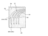
本実施形態では、上述の第1実施形態(図1参照)のものに対し、曲線光導波路を備える光導波路構造体の構成、及び、複数の曲線光導波路及び複数の光ファイバを用いて双方向通信を行なうようにすることで、多チャンネル化を実現している点で異なる。
つまり、上述の第1実施形態では、曲面上に形成された曲線光導波路を持つ光導波路構造体(光導波路が形成される平面が、光導波路の進行方向に沿った曲面となっているもの)を用いている。
In the present embodiment, a configuration of an optical waveguide structure including a curved optical waveguide, and a bidirectional configuration using a plurality of curved optical waveguides and a plurality of optical fibers, compared to the above-described first embodiment (see FIG. 1). It is different in that multi-channeling is realized by performing communication.
That is, in the first embodiment described above, an optical waveguide structure having a curved optical waveguide formed on a curved surface (the plane on which the optical waveguide is formed is a curved surface along the traveling direction of the optical waveguide). Is used.
また、上述の第1実施形態では、光導波路構造体を一つの曲線光導波路を備えるものとし、一つの曲線光導波路によって一本の光ファイバと一つの受光素子及び一つの発光素子とを光学的に接続して双方向通信を行なうようにしている。
これに対し、本実施形態では、図6に示すように、平面上に形成された曲線光導波路(曲げ導波路)21を持つ光導波路構造体20を用いている。なお、図6では、上述の第1実施形態及び変形例(例えば図1、図5参照)と同一のものには同一の符号を付している。
In the first embodiment described above, the optical waveguide structure is provided with one curved optical waveguide, and one optical fiber, one light receiving element, and one light emitting element are optically connected by one curved optical waveguide. Is connected to the two-way communication.
On the other hand, in this embodiment, as shown in FIG. 6, an
特に、本実施形態では、図6に示すように、光導波路構造体20を複数(ここでは4つ)の曲線光導波路21を備えるものとし、各曲線光導波路21の導波路コア24を、面型受光素子1及び面型発光素子2に接続される側の端面24Aへ向けて幅がテーパ状に広くなるようにしている。
また、本実施形態では、曲線光導波路21の導波路コア24の外側部分に対して、内側部分の長さを長くしている。つまり、曲線光導波路21の導波路コア24は、面型受光素子1及び面型発光素子2に接続される側の端面24Aへ向けて幅がテーパ状に広くなる第1領域(円弧状領域)と、第1領域の内側部分に連なり、幅及び厚さが一定の第2領域(直線状領域)とを備える。
In particular, in the present embodiment, as shown in FIG. 6, the
In the present embodiment, the length of the inner portion is made longer than the outer portion of the
このように、曲線光導波路21の導波路コア24の受光素子1及び発光素子2に接続される側の端面位置が、導波路コア24の外側部分と内側部分とでずらされている。
これは、光導波路構造体20に光学的に接続される受光素子アレイ1A及び発光素子アレイ2Aの設置スペースを確保するためである。
なお、導波路コア24の外側部分とは、導波路コア24の円弧状部分の径方向の外側部分をいい、導波路コア24の内側部分とは、導波路コア24の円弧状部分の径方向の内側部分をいう。
In this way, the end face position of the curved
This is to secure an installation space for the light
The outer portion of the
また、本実施形態では、光導波路構造体20は、曲線光導波路21の導波路コア24の受光素子1及び発光素子2に接続される側の端面24Aにミラー26A,26Bを備える。ここでは、導波路コア24の端面24Aを45度にカットしてミラー(45度カットミラー)26A,26Bを形成している。
具体的には、光導波路構造体20は、曲線光導波路21の導波路コア24の端面24Aの外側部分24aに第1ミラー26Aを備え、曲線光導波路21の導波路コア24の端面24Aの内側部分24bに第2ミラー26Bを備える。この場合、第1ミラー26Aと第2ミラー26Bとは、曲線光導波路21の導波路コア24の幅方向にずらされた位置に形成されることになる。
In this embodiment, the
Specifically, the
このように、光導波路構造体20は、曲線光導波路21の導波路コア24の外側部分を導かれた光を面型受光素子1へ導く第1ミラー26Aと、面型発光素子2から出射される光を曲線光導波路21の導波路コア24の内側部分へ導く第2ミラー26Bとを備える。つまり、光導波路構造体20は、曲線光導波路21の導波路コア24の端面24Aの外側部分24aと面型受光素子1との間に第1ミラー26Aが設けられている。また、曲線光導波路21の導波路コア24の端面24Aの内側部分24bと面型発光素子2との間に第2ミラー26Bが設けられている。
As described above, the
具体的には、光導波路構造体20は、例えば図7に示すように、平面基板(平板の表面)上に形成され、複数の曲線状の溝22を備えるクラッド構造体23と、各溝22に形成された導波路コア24と、複数の導波路コア24を覆うクラッドフィルム25とを備えるものとすれば良い。なお、図7では、説明の便宜上、ミラーを図示していない。
ここで、クラッド構造体23は、構造体表面の平面上に、複数の曲線状の溝22(導波路用溝;細溝)を有する平面構造体である。
Specifically, for example, as shown in FIG. 7, the
Here, the
導波路コア24は、クラッド構造体23の平面表層部に形成された曲線状の溝22にコア材料(コア樹脂)を充填することによって形成される。このため、導波路コア24は、クラッド構造体23の表面に沿って曲線状に形成される。つまり、曲線光導波路21は、平面上に形成された導波路コア24を有する。
クラッドフィルム25は、クラッド構造体23の平面上の溝22に形成された導波路コア24を覆うようにラミネートされている。
The
The
ところで、本実施形態では、図6に示すように、光導波路構造体20の複数の曲線光導波路21のそれぞれによって、光ファイバ10と受光素子1及び発光素子2とを光学的に接続して双方向通信を行なうようにしている。
この場合、上述の複数の曲線光導波路21を備える光導波路構造体20のほかに、複数の光ファイバ10を備える光ファイバアレイ10A、複数の受光素子1を備える受光素子アレイ1A、複数の発光素子2を備える発光素子アレイ2Aを用いることになる。
By the way, in this embodiment, as shown in FIG. 6, both the
In this case, in addition to the
この場合、光モジュール30は、図6に示すように、平面上に複数の曲線光導波路21を有する光導波路構造体20と、面型受光素子アレイ1Aと、面型発光素子アレイ2Aとを備える多チャンネル光トランシーバである。
ここで、面型受光素子アレイ1Aは、表面に受光面を有する複数の面型受光素子1を含む。ここでは、面型受光素子アレイ1Aは、複数(ここでは4つ)のフォトダイオード1を備えるPDアレイチップである。
In this case, as shown in FIG. 6, the
Here, the surface light receiving
面型発光素子アレイ2Aは、表面に出射面を有する複数の面型発光素子2を含む。ここでは、面型発光素子アレイ2Aは、複数(ここでは4つ)の面発光レーザ2を備えるVCSELアレイチップある。
そして、本実施形態では、複数の曲線光導波路21の導波路コア24の端面24Aの外側部分24aのそれぞれに、面型受光素子アレイ1Aに含まれる複数の面型受光素子1が、それぞれ、光学的に接続されている。
The surface light emitting
In this embodiment, each of the plurality of surface
また、複数の曲線光導波路21の導波路コア24の端面24Aの内側部分24bのそれぞれに、面型発光素子アレイ2Aに含まれる複数の面型発光素子2が、それぞれ、光学的に接続されている。
ここでは、光導波路構造体20に備えられる複数の曲線光導波路21が並んでいる方向に沿って平行に面型受光素子アレイ1A及び面型発光素子アレイ2Aが配置され、第1ミラー26A及び第2ミラー26Bを介して光学的に接続される。また、面型受光素子アレイ1Aと面型発光素子アレイ2Aとは、曲線光導波路21の導波路コア24が延びる方向にずらされて配置されている。また、面型受光素子1と面型発光素子2とは、曲線光導波路21の導波路コア24の幅方向(溝の幅方向)にずらされて配置されている。
The plurality of surface
Here, the planar light receiving
このように、本実施形態では、光導波路構造体20に備えられる各曲線光導波路21の一の端面24Aには、それぞれ、面型受光素子1及び面型発光素子2が第1ミラー26A及び第2ミラー26Bを介して光学的に接続されている。また、各曲線光導波路21の他の端面24Bには、それぞれ、光ファイバ10が光学的に接続されている。このようにして、同一平面上に形成された複数の曲線光導波路21のそれぞれによって、光ファイバ10と面型受光素子1及び面型発光素子2とが光学的に接続されている。
As described above, in the present embodiment, the surface
このため、各面型発光素子2から出射された光は、それぞれ、曲線光導波路21を導かれ、光ファイバ10に結合するとともに、各光ファイバ10から入射された光も、それぞれ、同一の曲線光導波路21を導かれ、面型受光素子1に結合することになる。つまり、各曲線光導波路21は、光ファイバ10と面型受光素子1とを接続する受信側光導波路(受信チャネル)として機能するとともに、光ファイバ10と面型発光素子2とを接続する送信側光導波路(送信チャネル)としても機能する。
For this reason, the light emitted from each surface
このように、本実施形態では、複数の曲線光導波路21及び複数の光ファイバ10のそれぞれによって双方向通信が可能になっている。また、ミラー26A,26Bを利用して曲線光導波路21と受光素子1及び発光素子2とを光学的に接続するようにしており、モジュール全体として低背化が可能になる。
したがって、本実施形態にかかる光導波路構造体及び光モジュールによれば、双方向通信を行なうため、光導波路構造体20に接続される光ファイバ10の本数を増やすことなく、チャンネル数を増加させることができるという利点がある。また、配線スペースの減少にもつながる。また、双方向通信を行なう場合に、光ファイバ10と受光素子1及び発光素子2とを光学的に接続する際の損失を低減することができるという利点もある。
As described above, in the present embodiment, bidirectional communication is possible by each of the plurality of curved
Therefore, according to the optical waveguide structure and the optical module according to the present embodiment, in order to perform bidirectional communication, the number of channels can be increased without increasing the number of
なお、本発明は、上述した第2実施形態に記載した構成に限定されるものではなく、本発明の趣旨を逸脱しない範囲で種々変形することが可能である。
例えば、上述の実施形態では、光導波路構造体20の下方に面型受光素子1及び面型発光素子2が実装された基板を配置するようにしているが、これに限られるものではない。例えば図8に示すように、光導波路構造体20の上方に面型受光素子1及び面型発光素子2が実装された基板27を配置するようにしても良い。なお、図8では、上述の実施形態(図6参照)と同一のものには同一の符号を付している。
The present invention is not limited to the configuration described in the second embodiment described above, and various modifications can be made without departing from the spirit of the present invention.
For example, in the above-described embodiment, the substrate on which the surface light-receiving
以下、実施例によって更に詳細に説明する。ただし、本発明は以下の実施例によって限定されるものではない。
[実施例1]
本実施例1では、図9に示すように、曲面上に曲線光導波路3を有し、曲線光導波路3の導波路コア6の端面6Aに傾斜面6xを有する光導波路構造体(ポリマ光導波路)4のサンプルを作製し、送受性能、即ち、光ファイバ10、受光素子1、発光素子2との間の損失を評価した。なお、この光導波路構造体4は、端面6Aに傾斜面6x及び平面(垂直面)6yの角度の異なる2つの面を有する。
Hereinafter, it demonstrates still in detail according to an Example. However, the present invention is not limited to the following examples.
[Example 1]
In the first embodiment, as shown in FIG. 9, an optical waveguide structure (polymer optical waveguide) having a curved
本実施例1では、光導波路構造体4を射出成型(モールド成型)によって作製して用いた。
つまり、まず、導波路コア6用の溝7を形成する部分が凸状になるように薄い板を重ねて金型40を作製した(図10参照)。そして、この金型40を用いて高温でクラッド用の樹脂を流し込み、冷却した後、金型40を抜いて、導波路コア6用の凹状の溝7が形成されたクラッド構造体8を作製した(図10参照)。流し込む樹脂材料はオレフィン樹脂とした。波長850nmでの屈折率は1.5であった。
In the present Example 1, the optical waveguide structure 4 was produced and used by injection molding (mold molding).
That is, first, a mold 40 was manufactured by stacking thin plates so that the portion where the
また、上述のように射出成型によってクラッド構造体8を作製する際に、溝7の延長線上の両端面に外向きに凸の半球面レンズ11,12,13を一体形成した。ここでは、受光素子1及び発光素子2に接続される側の端面には、溝7の深さ方向に並ぶように2つの半球面レンズ11,12を形成した。
ここでは、導波路コア6用の溝7は、幅を50μmとし、受光素子1及び発光素子2に接続される側の端面6Aへ向けて、深さが50μmから80μmへと広がるように形成し、端面6Aに45度傾斜面6xを形成した。このようにして、発光素子2からの光と光ファイバ10からの光との光線分離を行なえるようにした。
Further, when the
Here, the
次に、上述のようにして作製したクラッド構造体8の曲面上の溝7にコア液を滴下し、コア液が充填された溝7の上部をクラッドフィルム9で覆うことで、クラッドフィルム9によってコア液を封止し、コア液を硬化させて、導波路構造を形成した。
ここでは、コア液(ポリマ液)には、硬化後の屈折率が1.56となる紫外線硬化型エポキシ樹脂を用いた。
Next, the core liquid is dropped into the
Here, an ultraviolet curable epoxy resin having a refractive index after curing of 1.56 was used for the core liquid (polymer liquid).
クラッドフィルム9には、厚さ40μmのオレフィン樹脂製のフィルム(透明フィルム;オレフィンフィルム)を用いた。波長850nmでの屈折率は1.5であった。
このようにして、曲面上に曲線光導波路3を備え、単一導波路での双方向通信可能な光導波路構造体4のサンプルを作製した。
次に、上述のようにして作製した本実施例1のサンプル4を、以下のようにして評価した。
For the clad film 9, an olefin resin film (transparent film; olefin film) having a thickness of 40 μm was used. The refractive index at a wavelength of 850 nm was 1.5.
In this manner, a sample of the optical waveguide structure 4 having the curved
Next, the sample 4 of Example 1 manufactured as described above was evaluated as follows.
送信性能、即ち、発光素子−光ファイバ間の光結合損失の評価は、以下のようにして行なった。
光源として波長850nmの発光素子(面発光レーザ)2を用い、基板上に実装された面発光レーザ2の発光面(発光径10μm)上に、本実施例1のサンプル4をアライメントして設置し、サンプル4を通過して反対側に出てきた光を、自動調芯したGI型マルチモード光ファイバ(コア径50μm)10で受け、光パワーメータで出力を測定した。
Evaluation of transmission performance, that is, optical coupling loss between the light emitting element and the optical fiber was performed as follows.
A light emitting element (surface emitting laser) 2 having a wavelength of 850 nm is used as a light source, and the sample 4 of Example 1 is aligned and placed on the light emitting surface (light emitting diameter: 10 μm) of the
受信性能、即ち、光ファイバ−受光素子間の光結合損失の評価は、以下のようにして行なった。
波長850nmの外部光源からの光を、GI型マルチモード光ファイバ(コア径50μm)10を介して、本実施例1のサンプル4の光ファイバ側の端面まで導き、サンプル4を通過して反対側に出てきた光を、自動調芯したGI型マルチモード光ファイバ(コア径100μm)で受け、光パワーメータで出力を測定した。なお、ここでは、光結合損失を、より正確に測定するために、基板上に実装された受光素子(フォトディテクタ)1の受光面(受光径100μm)と同じ直径のコアを持つ光ファイバで受けて、光パワーメータで出力を測定するようにしている。
The reception performance, that is, the optical coupling loss between the optical fiber and the light receiving element was evaluated as follows.
Light from an external light source having a wavelength of 850 nm is guided to the end face on the optical fiber side of the sample 4 of the first embodiment through the GI type multimode optical fiber (core diameter 50 μm) 10, and passes through the sample 4 to the opposite side. Was received by a self-aligned GI type multimode optical fiber (core diameter 100 μm), and the output was measured with an optical power meter. Here, in order to measure the optical coupling loss more accurately, it is received by an optical fiber having a core having the same diameter as the light receiving surface (light receiving diameter of 100 μm) of the light receiving element (photodetector) 1 mounted on the substrate. The output is measured with an optical power meter.
光ファイバ10から本実施例1のサンプル4を通過して出てきた光がどの程度発光素子2側へ漏れているかの評価も、以下のようにして行なった。
波長850nmの外部光源からの光を、GI型マルチモード光ファイバ(コア径50μm)10を介して、本実施例1のサンプル4の光ファイバ10側の端面まで導き、サンプル4を通過して反対側に出てきた光を、自動調芯したGI型マルチモード光ファイバ(コア径100μm)で受け、光パワーメータで出力を測定した。
Evaluation of how much light emitted from the
Light from an external light source having a wavelength of 850 nm is guided to the end face on the
なお、ここでは、受光素子1と発光素子2との間の距離は約250μmとした。
この結果、本実施例1のサンプル4を用いた場合の発光素子−光ファイバ間の光結合損失は4.5dB程度であった。また、光ファイバ−受光素子間の光結合損失は5.0dB程度であった。また、発光素子2側への漏れ損失は8.5dB程度であった。
このように、本実施例1のサンプル4を用いることで、光ファイバ10からの光が受光素子1側に多く結合するようになり、単一導波路3で双方向通信を行なう場合に損失を低減できることが確認できた。
[実施例2]
本実施例2では、図11に示すように、曲面上に曲線光導波路3を有し、曲線光導波路3の導波路コア6の端面6Bが平面になっている光導波路構造体(ポリマ光導波路)4のサンプルを作製し、送受性能、即ち、光ファイバ、受光素子、発光素子との間の損失を評価した。
Here, the distance between the
As a result, the optical coupling loss between the light emitting element and the optical fiber in the case where the sample 4 of Example 1 was used was about 4.5 dB. The optical coupling loss between the optical fiber and the light receiving element was about 5.0 dB. Moreover, the leakage loss to the
As described above, by using the sample 4 of the first embodiment, a large amount of light from the
[Example 2]
In the second embodiment, as shown in FIG. 11, an optical waveguide structure (polymer optical waveguide) having a curved
本実施例2のサンプル4は、端面に傾斜面を形成せずに、端面6Bを平面(垂直面)にしたことを除いて、上述の実施例1の場合と同様に作製した。
また、本実施例2のサンプル4の評価も、上述の実施例1の場合と同様に行なった。但し、受光素子1と発光素子2との間の距離は約220μmとした。
この結果、本実施例2のサンプル4を用いた場合の発光素子−光ファイバ間の光結合損失は4.8dB程度であった。また、光ファイバ−受光素子間の光結合損失は4.3dB程度であった。また、発光素子2側への漏れ損失は8.3dB程度であった。
Sample 4 of Example 2 was produced in the same manner as in Example 1 except that the
The evaluation of Sample 4 of Example 2 was also performed in the same manner as in Example 1 described above. However, the distance between the
As a result, the optical coupling loss between the light emitting element and the optical fiber in the case where the sample 4 of Example 2 was used was about 4.8 dB. The optical coupling loss between the optical fiber and the light receiving element was about 4.3 dB. The leakage loss to the
このように、本実施例2のサンプル4を用いることで、光ファイバ10からの光が受光素子1側に多く結合するようになり、曲線光導波路3の導波路コア6の端面に傾斜面を形成せずに、端面6Bを平面(垂直面)にし、広げただけでも、単一導波路3で双方向通信を行なう場合に損失を低減できることが確認できた。
したがって、本実施例1、2のサンプル4を用いることで、単一光導波路3での双方向通信が可能となる。また、実装面積あたりのチャンネル数を増加させることができる。例えば双方向通信を行わないものと比較すると2倍のチャンネル数の増加が見込める。また、配線数の減少が可能となる。例えばチャンネル数が同じであれば、使用する光ファイバの本数を半分に削減することが可能となる。
As described above, by using the sample 4 of Example 2, a large amount of light from the
Therefore, by using the sample 4 of the first and second embodiments, bidirectional communication with the single
1 面型受光素子
1A 面型受光素子アレイ
2 面型発光素子
2A 面型発光素子アレイ
3 曲線光導波路
4,4A 光導波路構造体
5,5A,5X,30 光モジュール
6 導波路コア
6A,6B,6C,6D 端面
6a,6d,6f 第1傾斜面
6b,6e,6g 第2傾斜面
6x 傾斜面
6y 平面(垂直面)
7 溝
8 クラッド構造体
9 クラッドフィルム
10 光ファイバ
10A 光ファイバアレイ
11 第1レンズ
11A 第1レンズアレイ
12 第2レンズ
12A 第2レンズアレイ
13 第3レンズ
13A 第3レンズアレイ
14 プリント基板
20 光導波路構造体
21 曲線光導波路
22 溝
23 クラッド構造体
24 導波路コア
24A 端面
24a 外側部分
24b 内側部分
25 クラッドフィルム
26A 第1ミラー
26B 第2ミラー
27 基板
40 金型
DESCRIPTION OF
7
Claims (6)
前記曲線光導波路は、前記受光素子及び前記発光素子に接続される側の端面へ向けて幅又は厚さがテーパ状に大きくなる導波路コアを有し、
前記導波路コアの外側部分に光学的に接続された受光素子と、
前記導波路コアの内側部分に光学的に接続された発光素子とを備えることを特徴とする光モジュール。 An optical waveguide structure having a curved optical waveguide that optically connects an optical fiber, a light receiving element, and a light emitting element,
The curved optical waveguide has a waveguide core whose width or thickness increases in a tapered manner toward an end face on the side connected to the light receiving element and the light emitting element,
A light receiving element optically connected to an outer portion of the waveguide core;
An optical module comprising: a light emitting element optically connected to an inner portion of the waveguide core.
前記曲線光導波路は、前記受光素子及び前記発光素子に接続される側の端面へ向けて幅又は厚さがテーパ状に大きくなる導波路コアを有し、
前記導波路コアの外側部分から出射される光を前記受光素子へ導く第1レンズ又は第1ミラーと、
前記発光素子から出射される光を前記導波路コアの内側部分へ導く第2レンズ又は第2ミラーとを備えることを特徴とする光導波路構造体。 A curved optical waveguide that optically connects an optical fiber to a light receiving element and a light emitting element,
The curved optical waveguide has a waveguide core whose width or thickness increases in a tapered manner toward an end face on the side connected to the light receiving element and the light emitting element,
A first lens or a first mirror for guiding light emitted from an outer portion of the waveguide core to the light receiving element;
An optical waveguide structure comprising: a second lens or a second mirror that guides light emitted from the light emitting element to an inner portion of the waveguide core.
前記溝に形成された前記導波路コアと、
前記導波路コアを覆うクラッドフィルムとによって構成され、
前記導波路コアは、前記受光素子及び前記発光素子に接続される側の端面へ向けて厚さがテーパ状に厚くなっており、
前記導波路コアの外側部分から出射される光を前記受光素子へ導く第1レンズと、
前記発光素子から出射される光を前記導波路コアの内側部分へ導く第2レンズとを備えることを特徴とする、請求項2記載の光導波路構造体。 A clad structure having a groove formed on a curved surface;
The waveguide core formed in the groove;
A clad film covering the waveguide core;
The waveguide core has a thickness that is tapered toward the end face on the side connected to the light receiving element and the light emitting element,
A first lens for guiding light emitted from an outer portion of the waveguide core to the light receiving element;
The optical waveguide structure according to claim 2, further comprising a second lens that guides light emitted from the light emitting element to an inner portion of the waveguide core.
前記導波路コアは、前記受光素子及び前記発光素子に接続される側の端面へ向けて幅がテーパ状に広くなっており、
前記導波路コアの外側部分から出射される光を前記受光素子へ導く第1ミラーと、
前記発光素子から出射される光を前記導波路コアの内側部分へ導く第2ミラーとを備えることを特徴とする、請求項2記載の光導波路構造体。 The curved optical waveguide has the waveguide core formed on a plane,
The waveguide core has a width that is increased in a tapered shape toward an end face on a side connected to the light receiving element and the light emitting element,
A first mirror for guiding light emitted from an outer portion of the waveguide core to the light receiving element;
The optical waveguide structure according to claim 2, further comprising a second mirror that guides light emitted from the light emitting element to an inner portion of the waveguide core.
Priority Applications (1)
| Application Number | Priority Date | Filing Date | Title |
|---|---|---|---|
| JP2009134699A JP5206592B2 (en) | 2009-06-04 | 2009-06-04 | Optical module and optical waveguide structure |
Applications Claiming Priority (1)
| Application Number | Priority Date | Filing Date | Title |
|---|---|---|---|
| JP2009134699A JP5206592B2 (en) | 2009-06-04 | 2009-06-04 | Optical module and optical waveguide structure |
Publications (2)
| Publication Number | Publication Date |
|---|---|
| JP2010281988A true JP2010281988A (en) | 2010-12-16 |
| JP5206592B2 JP5206592B2 (en) | 2013-06-12 |
Family
ID=43538765
Family Applications (1)
| Application Number | Title | Priority Date | Filing Date |
|---|---|---|---|
| JP2009134699A Expired - Fee Related JP5206592B2 (en) | 2009-06-04 | 2009-06-04 | Optical module and optical waveguide structure |
Country Status (1)
| Country | Link |
|---|---|
| JP (1) | JP5206592B2 (en) |
Citations (8)
| Publication number | Priority date | Publication date | Assignee | Title |
|---|---|---|---|---|
| JPH11248952A (en) * | 1998-02-27 | 1999-09-17 | Hitachi Cable Ltd | Waveguide type optical isolator |
| JP2000147427A (en) * | 1998-11-06 | 2000-05-26 | Hitachi Cable Ltd | Waveguide type optical circulator |
| JP2005070189A (en) * | 2003-08-20 | 2005-03-17 | Yazaki Corp | Optical link for luminous flux multiplex communication, and optical link for two-way optical communication |
| JP2005115346A (en) * | 2003-09-17 | 2005-04-28 | Fujitsu Ltd | Optical waveguide structure and optical module |
| JP2007003817A (en) * | 2005-06-23 | 2007-01-11 | Fujitsu Ltd | Optical waveguide structure, optical module, and lens array |
| JP2007094193A (en) * | 2005-09-29 | 2007-04-12 | Rohm Co Ltd | Optical communication module |
| JP2007264033A (en) * | 2006-03-27 | 2007-10-11 | Fujitsu Ltd | Optical module, optical transmission system, and manufacturing method of optical module |
| JP2009037054A (en) * | 2007-08-02 | 2009-02-19 | Sony Corp | Optical module and its manufacturing method |
-
2009
- 2009-06-04 JP JP2009134699A patent/JP5206592B2/en not_active Expired - Fee Related
Patent Citations (8)
| Publication number | Priority date | Publication date | Assignee | Title |
|---|---|---|---|---|
| JPH11248952A (en) * | 1998-02-27 | 1999-09-17 | Hitachi Cable Ltd | Waveguide type optical isolator |
| JP2000147427A (en) * | 1998-11-06 | 2000-05-26 | Hitachi Cable Ltd | Waveguide type optical circulator |
| JP2005070189A (en) * | 2003-08-20 | 2005-03-17 | Yazaki Corp | Optical link for luminous flux multiplex communication, and optical link for two-way optical communication |
| JP2005115346A (en) * | 2003-09-17 | 2005-04-28 | Fujitsu Ltd | Optical waveguide structure and optical module |
| JP2007003817A (en) * | 2005-06-23 | 2007-01-11 | Fujitsu Ltd | Optical waveguide structure, optical module, and lens array |
| JP2007094193A (en) * | 2005-09-29 | 2007-04-12 | Rohm Co Ltd | Optical communication module |
| JP2007264033A (en) * | 2006-03-27 | 2007-10-11 | Fujitsu Ltd | Optical module, optical transmission system, and manufacturing method of optical module |
| JP2009037054A (en) * | 2007-08-02 | 2009-02-19 | Sony Corp | Optical module and its manufacturing method |
Also Published As
| Publication number | Publication date |
|---|---|
| JP5206592B2 (en) | 2013-06-12 |
Similar Documents
| Publication | Publication Date | Title |
|---|---|---|
| US7609922B2 (en) | Optical module, optical transmission system, and fabrication method for optical module | |
| US7220065B2 (en) | Connection apparatus for parallel optical interconnect module and parallel optical interconnect module using the same | |
| US7539367B2 (en) | Optical system connection structure, optical component, and optical communication module | |
| CN106646772B (en) | Structure of photoelectric conversion module | |
| WO2018213035A1 (en) | Optical coupling structures | |
| US9160450B2 (en) | Multi-channel transceiver | |
| WO2011105078A1 (en) | Optical module | |
| JP2013205582A (en) | Optical receptacle and optical module including the same | |
| US20130094864A1 (en) | Optical interface for bidirectional communications | |
| US20150086165A1 (en) | Optical receptacle and optical module provided with same | |
| JP2008209767A (en) | Optical module and its manufacturing method | |
| JP6728639B2 (en) | Optical wiring connection structure and optical wiring connection method | |
| JP2008020721A (en) | Parallel optical transmitter-receiver | |
| JP2008020720A (en) | Optical waveguide and parallel optical transmitter-receiver | |
| JP5206592B2 (en) | Optical module and optical waveguide structure | |
| JP2008134444A (en) | Optical module and optical waveguide structure | |
| JP2008015040A (en) | Optical waveguide and optical module | |
| US9423581B2 (en) | Parallel optical system with integrated monitoring photodetectors | |
| JP2010020085A (en) | Optical waveguide structure and method of manufacturing the same, and optical module | |
| WO2016147300A1 (en) | Optical waveguide, method for manufacturing same, and optical device using said optical waveguide | |
| KR100398045B1 (en) | Module for transmitting and receiving an optic signal | |
| JP5056698B2 (en) | Optical waveguide structure | |
| JP2008233556A (en) | Lens case and optical module | |
| JP4196790B2 (en) | Optical transmission module | |
| JP2011053303A (en) | Optical element module, optical transceiver, and optical active cable |
Legal Events
| Date | Code | Title | Description |
|---|---|---|---|
| A621 | Written request for application examination |
Free format text: JAPANESE INTERMEDIATE CODE: A621 Effective date: 20120214 |
|
| A977 | Report on retrieval |
Free format text: JAPANESE INTERMEDIATE CODE: A971007 Effective date: 20121228 |
|
| TRDD | Decision of grant or rejection written | ||
| A01 | Written decision to grant a patent or to grant a registration (utility model) |
Free format text: JAPANESE INTERMEDIATE CODE: A01 Effective date: 20130122 |
|
| A61 | First payment of annual fees (during grant procedure) |
Free format text: JAPANESE INTERMEDIATE CODE: A61 Effective date: 20130204 |
|
| FPAY | Renewal fee payment (event date is renewal date of database) |
Free format text: PAYMENT UNTIL: 20160301 Year of fee payment: 3 |
|
| R150 | Certificate of patent or registration of utility model |
Free format text: JAPANESE INTERMEDIATE CODE: R150 |
|
| LAPS | Cancellation because of no payment of annual fees |