JP2010271663A - Electrostatically-driven optical scanner - Google Patents
Electrostatically-driven optical scanner Download PDFInfo
- Publication number
- JP2010271663A JP2010271663A JP2009125706A JP2009125706A JP2010271663A JP 2010271663 A JP2010271663 A JP 2010271663A JP 2009125706 A JP2009125706 A JP 2009125706A JP 2009125706 A JP2009125706 A JP 2009125706A JP 2010271663 A JP2010271663 A JP 2010271663A
- Authority
- JP
- Japan
- Prior art keywords
- mirror
- light
- axis
- region
- positive
- Prior art date
- Legal status (The legal status is an assumption and is not a legal conclusion. Google has not performed a legal analysis and makes no representation as to the accuracy of the status listed.)
- Pending
Links
- 230000003287 optical effect Effects 0.000 title 1
- 238000001514 detection method Methods 0.000 claims abstract description 36
- 230000001678 irradiating effect Effects 0.000 claims description 4
- 230000010355 oscillation Effects 0.000 description 7
- 238000000034 method Methods 0.000 description 6
- 230000002093 peripheral effect Effects 0.000 description 6
- 239000011159 matrix material Substances 0.000 description 3
- 230000004397 blinking Effects 0.000 description 1
- 230000007423 decrease Effects 0.000 description 1
- 230000003247 decreasing effect Effects 0.000 description 1
- 238000010586 diagram Methods 0.000 description 1
Images

Landscapes
- Mechanical Optical Scanning Systems (AREA)
- Mechanical Light Control Or Optical Switches (AREA)
Abstract
Description
本発明は、光を所望の方向に反射するマイクロミラー装置に関する。 The present invention relates to a micromirror device that reflects light in a desired direction.
従来、微小機械システム(MEMS)を用いて、光を所望の方向に反射するマイクロミラー装置が知られている(特許文献1)。 2. Description of the Related Art Conventionally, a micromirror device that reflects light in a desired direction using a micro mechanical system (MEMS) is known (Patent Document 1).
しかし、MEMSの揺動範囲には限りがあるため光の反射範囲が限定される。光の反射範囲を広げるため、MEMSから受光板までの距離を広げると光の精細度が低下する。 However, since the MEMS swing range is limited, the light reflection range is limited. If the distance from the MEMS to the light receiving plate is increased in order to widen the light reflection range, the definition of the light decreases.
本発明は、これらの問題を鑑みてなされたものであり、1つの光源を用いて広範囲に渡って光を精細に反射することが可能なマイクロミラー装置を得ることを目的とする。 The present invention has been made in view of these problems, and an object of the present invention is to obtain a micromirror device capable of finely reflecting light over a wide range using a single light source.
本発明による描画装置は、受光板に向けて光を照射して描画を行う描画装置であって、光を射出する1つの光源部材と、受光板に向けて光を反射しうる複数のミラー部材と、光源部材が射出した光を複数のミラー部材に向けて交互に反射する光切替部材とを備えることを特徴とする。 A drawing apparatus according to the present invention is a drawing apparatus that performs drawing by irradiating light toward a light receiving plate, and includes a single light source member that emits light and a plurality of mirror members that can reflect light toward the light receiving plate. And a light switching member that alternately reflects light emitted from the light source member toward a plurality of mirror members.
ミラー部材は所定の軸周りに揺動可能であって、ミラー部材の揺動周波数、揺動角度、及び位相を制御する制御部材とをさらに備えることが好ましい。 The mirror member is preferably swingable about a predetermined axis, and further preferably includes a control member for controlling the swing frequency, swing angle, and phase of the mirror member.
ミラー部材は、第1のミラー部材と第2のミラー部材とを備え、第1のミラー部材は、受光板上の描画領域における第1の領域に光を照射可能であって、第2のミラー部材は、描画領域において第1の領域とわずかに重複する第2の領域に光を照射可能であって、制御部材は、第1の領域に照射される光の軌跡と第2の領域に照射される光の軌跡とが略連続となるように第1及び第2のミラー部材を制御することが好ましい。 The mirror member includes a first mirror member and a second mirror member, and the first mirror member can irradiate light to the first region in the drawing region on the light receiving plate, and the second mirror The member can irradiate light in a second region slightly overlapping with the first region in the drawing region, and the control member irradiates the second region with a locus of light radiated to the first region. It is preferable to control the first and second mirror members so that the locus of the emitted light is substantially continuous.
第1のミラー部材は、平面である第1の鏡面を有し、第1の鏡面と平行な第1の軸周り、及び第1の鏡面と平行かつ第1の軸と直交する第2の軸周りに揺動自在であって、第2のミラー部材は、平面である第2の鏡面を有し、第1の鏡面及び第2の鏡面と平行な第3の軸周り、並びに第2の鏡面と平行かつ第3の軸と直交する第4の軸周りに揺動自在であって、光切替部材は、第1及び第3の軸と平行な第5の軸周りに揺動自在であることが好ましい。 The first mirror member has a first mirror surface which is a flat surface, and has a first axis parallel to the first mirror surface, and a second axis parallel to the first mirror surface and perpendicular to the first axis. The second mirror member has a second mirror surface that is a plane, and is movable around the third axis parallel to the first mirror surface and the second mirror surface, and the second mirror surface. And the light switching member is swingable about a fifth axis parallel to the first and third axes. Is preferred.
第5の軸は、第1の軸からの距離と第3の軸からの距離とが等しく、かつ第2の軸からの距離と第4の軸からの距離とが等しいことが好ましい。 The fifth axis preferably has the same distance from the first axis as the distance from the third axis, and the same distance from the second axis and the distance from the fourth axis.
制御部材は、ミラー部材に印加する交流電圧の振幅を変化可能であっても良い。 The control member may be capable of changing the amplitude of the AC voltage applied to the mirror member.
制御部材は、ミラー部材に印加する交流電圧の周波数を変化可能であっても良い。 The control member may be capable of changing the frequency of the alternating voltage applied to the mirror member.
制御部材は、第1のミラー部材と第2のミラー部材に各々印加する2つの交流電圧に位相差を設けるように構成されても良い。 The control member may be configured to provide a phase difference between two AC voltages applied to the first mirror member and the second mirror member, respectively.
受光板の描画領域外に設けられ、切替部材からの光を受光可能である光検知部材をさらに備え、ミラー制御部材は、光検知部材が受光した光の位置に応じてミラー部材の揺動周波数、振動角度、及び位相を制御することが好ましい。 A light detection member provided outside the drawing area of the light receiving plate and capable of receiving light from the switching member is further provided, and the mirror control member has a swing frequency of the mirror member according to the position of the light received by the light detection member. It is preferable to control the vibration angle and the phase.
ミラー部材が反射した光は受光板上において線分状の軌跡を成し、複数の光検出部材は、ミラー部材からの反射光により受光板上に形成される軌跡が伸びる方向に対して直線状に並べられ、ミラー制御部材は、光を検出した光検出部材の位置に応じてミラー部材の振幅を制御することが好ましい。 The light reflected by the mirror member forms a line-shaped locus on the light receiving plate, and the plurality of light detection members are linear with respect to the direction in which the locus formed on the light receiving plate by the reflected light from the mirror member extends. The mirror control member preferably controls the amplitude of the mirror member in accordance with the position of the light detection member that detects the light.
光検出部材はフォトダイオードであって、光を受光すると電流値が変化し、ミラー制御部は光検出部材による電流の変化に応じてミラー部を制御することが好ましい。 It is preferable that the light detection member is a photodiode, and the current value changes when light is received, and the mirror control unit controls the mirror unit according to a change in current by the light detection member.
本発明によれば、1つの光源を用いて広範囲に渡って光を精細に反射することが可能なマイクロミラー装置を得る。 According to the present invention, a micromirror device capable of finely reflecting light over a wide range using a single light source is obtained.
以下、本発明による描画装置10の一実施形態について図を用いて説明する。図1から3に描画装置10及び周辺装置の構成を示す。
Hereinafter, an embodiment of a
描画装置10は、光源部材であるレーザダイオード(LD)11、光切替部材である切替ミラー12、及びミラー部材である第1及び第2の描画ミラー13、14を備える。
The
レーザダイオード11はレーザ光を射出する。切替ミラー12は、MMD(Micro Mirror Device)から成り、平面かつ正方形の鏡面15を有する。第1及び第2の描画ミラー13、14は、MEMSから成り、平面かつ正方形の鏡面16、17を有する。
The
描画装置10は、照射対象面20に向けてレーザ光を照射する。照射対象面20は平面であって、レーザ光により任意の画像が描かれる長方形の描画領域21と、描画領域21の外側に設けられる光検出部材22とを有する。
The
以下、描画領域21の長辺が伸びる方向をX軸方向、短辺が伸びる方向をY軸方向、描画領域21に対して直角方向であって描画装置10が設けられる方向をZ軸正方向、原点を描画領域21の中心Oとして説明する。この座標系は右手系である。なお、図1に示す座標は、参照を容易にするため、原点をずらして表示している。
Hereinafter, the direction in which the long side of the
光検出部材22は、フォトダイオードから成り、描画領域21におけるX軸正方向外側に設けられる第1のX方向光検知部材PD1xと、描画領域21におけるX軸負方向外側に設けられる第2のX方向光検知部材PD2xと、描画領域21のY軸負方向外側に設けられる第1及び第2のY方向光検知部材PD1y、PD2yとを有する。
The
第1及び第2のX方向光検知部材PD1x、PD2xは、描画領域21の短辺中央に設けられる。第1のY方向光検知部材PD1yは、描画領域21の長辺を四等分する位置のうちX軸正方向側に設けられ、第2のY方向光検知部材PD2yは、描画領域21の長辺を四等分する位置のうちX軸負方向側に設けられる。
The first and second X-direction light detection members PD1x and PD2x are provided at the center of the short side of the
レーザダイオード11は、Z軸負方向にレーザ光を射出する。射出されたレーザ光は切替ミラー12に照射される。
The
切替ミラー12は、描画領域21から一定の距離を置いて設けられ、描画領域21の短辺と平行である、すなわちY軸方向に伸びる切替ミラー軸lm回りに回動する。回動する範囲は、YZ平面を中心として±45度、すなわち90度である。切替ミラー軸lmは、描画領域21の中心を通りかつ描画領域21に対して直角な直線と交わる。切替ミラー12が有する鏡面15の中心部にレーザ光が照射される。切替ミラー12が、切替ミラー軸lmに関してY軸正方向右回転方向に最も回動したとき、レーザ光は第1の描画ミラー13に向けて反射される。切替ミラー12が、切替ミラー軸lmに関してY軸正方向左回転方向に最も回動したとき、レーザ光は第2の描画ミラー14に向けて反射される。切替ミラー12が回動することにより、第1及び第2の描画ミラー13、14に向けてレーザ光が交互に照射される。
The
第1及び第2の描画ミラー13、14は、描画領域21から一定の距離を置いて設けられ、2つの軸回りに揺動する第1及び第2の可動ミラー(不図示)を各々備える。第1及び第2の可動ミラーは鏡面16、17を有する。第1及び第2の描画ミラー13、14は、YZ平面に対して対称位置に設けられる。
The first and
第1の描画ミラー13は、照射対象面20に対して135度の角度を有する第1のY照射軸ly1、及びY軸に対して平行な第1のX照射軸lx1回りに回動する。回動する範囲は、第1の描画ミラー13と描画領域21との距離、描画する範囲に応じて定められる。切替ミラー12から第1の可動ミラーに向けて照射されたレーザ光は、第1の可動ミラーにより反射されて照射対象面20に向けて照射される。第1の可動ミラーは、第1のY照射軸及び第1のX照射軸回りに回動して、描画領域21の略半分、すなわちXY平面における第1及び第4象限とその周辺領域にレーザ光を反射する。第1の可動ミラーの鏡面と第1のX照射軸lx1及び第1のY照射軸ly1は平行である。また、第1のX照射軸lx1は第1のY照射軸ly1と直交する。
The
第2の描画ミラー14は、照射対象面20に対して45度の角度を有する第2のY照射軸ly2、及びY軸に対して平行な第2のX照射軸lx2回りに回動する。回動する範囲は、第2の描画ミラー14と描画領域21との距離、描画する範囲に応じて定められる。切替ミラー12から第2の可動ミラーに向けて照射されたレーザ光は、第2の可動ミラーにより反射されて照射対象面20に向けて照射される。第2の可動ミラーは、第2のY照射軸及び第2のX照射軸回りに回動して、描画領域21の略半分、すなわちXY平面における第2及び第3象限とその周辺領域にレーザ光を反射する。第2の可動ミラーの鏡面と第2のX照射軸lx2及び第2のY照射軸ly2は平行である。また、第2のX照射軸lx2は第2のY照射軸ly2と直交する。第1のY照射軸ly1、第2のY照射軸ly2、及び切替ミラー軸lmは互いに平行である。
The
レーザダイオード11が照射したレーザ光を、切替ミラー12が第1の描画ミラー13に向けて照射する。第1の描画ミラー13は、照射対象面20において、X軸正方向最大地点からY軸(X=0)をわずかに超える位置までレーザ光を照射する。次に切替ミラー12は90度回動し、第2の描画ミラー14に向けてレーザ光を照射する。第2の描画ミラー14は、照射対象面20において、Y軸(X=0)をX軸正方向にわずかに超える位置からX軸負方向最大地点までレーザ光を照射する。第2の描画ミラー14が照射対象面20にレーザ光を照射する間、第1の描画ミラー13は、照射対象面20におけるX軸正方向最大地点であって、前回の照射よりも1走査線分だけY軸負方向にずれた位置にレーザ光を照射可能な角度にまで回動する。
The switching
次に切替ミラー12は90度回動し、第1の描画ミラー13に向けてレーザ光を照射する。第1の描画ミラー13は、照射対象面20に向けて再度レーザ光を照射する。このとき照射される位置は、前回の照射よりも1走査線分だけY軸負方向にずれた位置である。第1の描画ミラー13が照射対象面20にレーザ光を照射する間、第2の描画ミラー14は、照射対象面20におけるY軸(X=0)をX軸正方向にわずかに超える位置であって、前回の照射よりも1走査線分だけY軸負方向にずれた位置にレーザ光を照射可能な角度にまで回動する。
Next, the switching
次に切替ミラー12は90度回動し、第2の描画ミラー14に向けてレーザ光を照射する。第2の描画ミラー14は、照射対象面20に向けて再度レーザ光を照射する。このとき照射される位置は、前回の照射よりも1走査線分だけY軸負方向にずれた位置である。
Next, the switching
これらの動作を繰り返すことにより、描画装置10は描画領域21の全域に渡ってレーザ光を照射する。
By repeating these operations, the
また、レーザダイオード11は、描画すべき画像に応じてレーザ光を明滅させながら照射する。そのため、描画装置10は描画領域21に任意の画像を描画できる。
The
すなわち、第1の描画ミラー13は、描画領域21のX正方向部分について描画を行い、第2の描画ミラー14は、描画領域21のX負方向部分について描画を行う。これにより、レーザ光が描画領域21から光検出部材22に渡って照射され、任意の画像が描画領域21に描画される。
That is, the
第1のX方向光検知部材PD1xは、第1から第9のX正方向フォトデテクタPD1x00、PD1x01、PD1x02、PD1x10、PD1x11、PD1x12、PD1x20、PD1x21、PD1x22から成る。これらのX正方向フォトデテクタは、X軸及びY軸の負方向から正方向に向けて第1から第9の順に並べられ、3行3列の正方行列を形成する。 The first X-direction light detection member PD1x includes first to ninth X-positive photodetectors PD1x00, PD1x01, PD1x02, PD1x10, PD1x11, PD1x12, PD1x20, PD1x21, and PD1x22. These X positive direction photodetectors are arranged in the first to ninth order from the negative direction of the X axis and the Y axis in the positive direction to form a 3 × 3 square matrix.
第2のX方向光検知部材PD2xは、第1から第9のX負方向フォトデテクタPD2x00、PD2x01、PD2x02、PD2x10、PD2x11、PD2x12、PD2x20、PD2x21、PD2x22から成る。これらのX負方向フォトデテクタは、X軸の正方向から負方向かつY軸の負方向から正方向に向けて第1から第9の順に並べられ、3行3列の正方行列を形成する。 The second X-direction light detection member PD2x includes first to ninth X-negative photodetectors PD2x00, PD2x01, PD2x02, PD2x10, PD2x11, PD2x12, PD2x20, PD2x21, and PD2x22. These X negative direction photodetectors are arranged in the first to ninth order from the positive direction of the X axis to the negative direction and from the negative direction of the Y axis to the positive direction to form a 3 × 3 square matrix.
第1のY方向光検知部材PD1yは、第11から第13のY方向フォトデテクタPD1y0、PD1y1、PD1y2から成り、第2のY方向光検知部材PD2yは、第21から第23のY方向フォトデテクタPD2y0、PD2y1、PD2y2から成る。これらのY方向フォトデテクタは、Y軸の正方向から負方向に向けて第11から第13、又は第21から第23の順に並べられ、3行1列の行列を各々形成する。各フォトデテクタは、光を受光するとアナログ信号を発する。 The first Y-direction light detection member PD1y includes eleventh to thirteenth Y-direction photodetectors PD1y0, PD1y1, and PD1y2, and the second Y-direction light detection member PD2y includes the twenty-first to twenty-third Y-direction photodetectors. It consists of PD2y0, PD2y1, and PD2y2. These Y-direction photodetectors are arranged in the order of 11th to 13th or 21st to 23rd from the positive direction to the negative direction of the Y-axis to form a matrix of 3 rows and 1 column. Each photo detector emits an analog signal when it receives light.
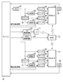
次に、図2を用いて描画装置10を制御する周辺装置について説明する。
Next, a peripheral device that controls the
周辺装置は、マイコン31、発振器(OCR)32、LD駆動回路33、MMD駆動回路34、第1及び第2のX方向反転器42、52、第1及び第2のX方向正電圧アンプ43、53、第1及び第2のX方向負電圧アンプ44、54、第1及び第2のカウンタ41、51、第1及び第2のY方向反転器45、55、第1及び第2のY方向正電圧アンプ46、56、第1及び第2のY方向負電圧アンプ47、57、光検出部材22とから主に構成される。
The peripheral devices include a
マイコン31は、描画すべき画像に応じてLD駆動回路33及びMMD駆動回路34に制御信号を送る。LD駆動回路33は、制御信号に応じてレーザダイオード11を駆動する。これにより、レーザダイオード11は描画すべき画像に応じて、レーザ光を明滅する。MMD駆動回路34は、制御信号に応じて切替ミラー12を駆動する。これにより、切替ミラー12は切替ミラー軸lm回りに所定の周期で回動する。
The
マイコン31は、各フォトデテクタに接続され、光を受光した光検出部材22から受信したアナログ信号に応じて、発振器32、第1及び第2のY方向正電圧アンプ46、56及び第1及び第2のY方向負電圧アンプ47、57を制御する。X軸方向の振幅を制御するため周波数制御信号が発振器32に送信される。Y軸方向の振幅を制御するため第1及び第2のY方向正電圧アンプ46、56及び第1及び第2のY方向負電圧アンプ47、57に電圧制御信号が送信される。
The
光検知部材から受信したアナログ信号の状態を記録するための状態変数をマイコン31が備える。第1から第9のX正方向フォトデテクタPD1x00−PD1x22に対して、第1から第9のX正方向状態変数V1x00−V1x22が各々対応し、第1から第9のX負方向フォトデテクタPD2x00−PD2x22に対して、第1から第9のX負方向状態変数V2x00−V2x22が各々対応する。そして、第11から第13及び第21から第23のY方向フォトデテクタPD1y0−PD1y2、PD2y0−PD2y2に対して、第11から第13及び第21から第23のY方向状態変数V1y0−V1y2、V2y0−V2y2が各々対応する。
The
発振器32は、マイコン31からの周波数制御信号に応じた周波数の交流信号を第1及び第2のX方向正電圧アンプ43、53、第1及び第2のX方向反転器42、52、及び第1及び第2のカウンタ41、51に送信する。発振器32は、VCO(電圧制御発振器)又はDDS(ダイレクト・デジタル・シンセサイザ)が用いられる。
The
第1及び第2のX方向反転器42、52は、受信した交流信号の位相を反転させ、反転した交流信号を第1及び第2のX方向負電圧アンプ44、54に送信する。第1及び第2のX方向正電圧アンプ43、53及び第1及び第2のX方向負電圧アンプ44、54は、第1及び第2の可動ミラーを駆動するに足る電圧まで交流信号を増幅し、第1及び第2の可動ミラーに交流信号を送信する。
The first and second X direction inverters 42 and 52 invert the phase of the received AC signal, and transmit the inverted AC signal to the first and second X direction
第1及び第2のX方向正電圧アンプ43、53及び第1及び第2のX方向負電圧アンプ44、54からの交流信号の周波数に応じた揺動周波数で、第1及び第2の可動ミラーが揺動する。交流信号の周波数が上げられると、第1及び第2の可動ミラーの揺動周波数が上がり、振幅が小さくなる。交流信号の周波数が下げられると、第1及び第2の可動ミラーの揺動周波数が下がり、振幅が大きくなる。
The first and second movable elements at an oscillation frequency corresponding to the frequency of the AC signal from the first and second X-direction
第1及び第2のカウンタ41、51は、発振器32が発信した信号の周波数を3/4に分周する。そして、分周した信号を第1及び第2のY方向正電圧アンプ46、56及び第1及び第2のY方向反転器30、45に送信する。第1及び第2のX方向反転器42、52と同様にして、第1及び第2のY方向反転器30、45は反転した交流信号を第1及び第2のY方向負電圧アンプ47、57に送信する。第1及び第2のY方向正電圧アンプ46、56及び第1及び第2のY方向負電圧アンプ47、57は、受信した交流信号の電圧、すなわち振幅をマイコン31からの電圧制御信号に応じて変化させた後、第1及び第2の可動ミラーに送信する。
The first and
第1及び第2の可動ミラーは、第1及び第2のY方向正電圧アンプ46、56及び第1及び第2のY方向負電圧アンプ47、57からの交流信号の周波数に応じた揺動周波数と電圧に応じた振幅とにより揺動する。交流信号の振幅が上げられると、第1及び第2の可動ミラーの振幅が大きくなる。交流信号の振幅が下げられると、第1及び第2の可動ミラーの振幅が小さくなる。このようにして、第1及び第2の可動ミラーにより反射されたレーザ光が照射対象面20上においてY軸正負方向に走査される。
The first and second movable mirrors oscillate in accordance with the frequency of the AC signal from the first and second Y-direction
第1及び第2のX方向正電圧アンプ43、53、第1及び第2のX方向負電圧アンプ44、54、第1及び第2のY方向正電圧アンプ46、56及び第1及び第2のY方向負電圧アンプ47、57は、第1及び第2の可動ミラーに交流信号を同時に印加する。そのため、第1及び第2の可動ミラーにより反射されたレーザ光は、照射対象面20上においてX軸正負方向及びY軸正負方向に同時に振れる。すなわち、第1及び第2の可動ミラーは、ラスタスキャンにより照射対象面20上にレーザ光を走査する。
First and second X-direction
X方向に対する駆動とY方向に対する駆動を同時に行う場合、X方向に対する駆動において共振現象を利用した制御を行っているため、Y方向に対する駆動において駆動周波数を変更しても振幅を必要量まで大きくすることができず、共振現象を利用できない。そのため、Y方向に対する駆動では、電圧を変更することで振幅を制御する。 When driving in the X direction and driving in the Y direction are performed at the same time, since the control using the resonance phenomenon is performed in the driving in the X direction, the amplitude is increased to the required amount even if the driving frequency is changed in the driving in the Y direction. And the resonance phenomenon cannot be used. Therefore, in driving in the Y direction, the amplitude is controlled by changing the voltage.
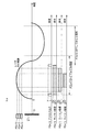
図3を用いて、レーザ光の照射範囲を検知する手段について説明する。簡単のため、第4、第5、第6のX正方向フォトデテクタPD1x10、PD1x11、PD1x12のみを用い説明する。 A means for detecting the irradiation range of the laser beam will be described with reference to FIG. For the sake of simplicity, description will be made using only the fourth, fifth, and sixth X-direction photodetectors PD1x10, PD1x11, and PD1x12.
図3における最上段の曲線は、照射対象面20上のX軸方向におけるレーザ光照射位置の時間変化を示す。レーザ光が描画領域21を大きく超えて照射される場合、及び描画領域21内にしか照射されていない場合、描画領域21に形成される情報、たとえば文字情報や画像情報の形状が崩れ、ユーザが情報を認識できなくなる。そのため、描画領域21をわずかに外す程度の範囲でレーザ光が走査されるように、描画手段が実行される。
The uppermost curve in FIG. 3 shows the time change of the laser beam irradiation position in the X-axis direction on the
描画領域21を外れたレーザ光が第4のX正方向フォトデテクタPD1x10に入射すると、第4のX正方向フォトデテクタPD1x10は、アナログ信号をマイコン31に送信する。
When the laser beam outside the
マイコン31は、アナログ信号を受信して、第4のX方向状態変数Vx10をONにする。
The
さらに、レーザ光が第5、第6のX正方向フォトデテクタPD1x11、PD1x12に入射すると、第5、第6のX正方向フォトデテクタPD1x11、PD1x12は、アナログ信号をマイコン31に送信する。マイコン31はアナログ信号を受信して、第5、第6のX方向状態変数V1x11、V1x12を各々ONにする。
Further, when the laser light is incident on the fifth and sixth X positive photo detectors PD1x11 and PD1x12, the fifth and sixth X positive photo detectors PD1x11 and PD1x12 transmit analog signals to the
次に、レーザ光がX軸正方向最大位置で折り返してX軸負方向に移動を始めると、第6のX正方向フォトデテクタPD1x12に入射する。レーザ光を受信した第6のX正方向フォトデテクタPD1x12がアナログ信号をマイコン31に送信すると、マイコン31はアナログ信号を受信して、第6のX方向状態変数V1x12をOFFにする。
Next, when the laser beam turns back at the maximum position in the X-axis positive direction and starts moving in the X-axis negative direction, it enters the sixth X-positive photo detector PD1x12. When the sixth X-positive photodetector PD1x12 that has received the laser beam transmits an analog signal to the
さらに、レーザ光が第5、第4のX正方向フォトデテクタPD1x11、PD1x10に入射すると、第5、第4のX正方向フォトデテクタPD1x11、PD1x10が、アナログ信号をマイコン31に送信する。マイコン31はアナログ信号を受信して、第5、第4のX方向状態変数V1x11、V1x10を各々OFFにする。
Further, when the laser light is incident on the fifth and fourth X positive photo detectors PD1x11 and PD1x10, the fifth and fourth X positive photo detectors PD1x11 and PD1x10 transmit analog signals to the
レーザ光が描画領域21を外れてから再度描画領域21内に戻るまでに必要な時間は、第1の可動ミラーのX軸方向周期の半分、すなわち半周期より短い。
The time required for the laser light to return to the
一方、マイコン31におけるX方向状態変数がOFFの時に、レーザ光がX軸正方向最大位置から描画領域21内へ向けて移動している場合がある。このとき、各X正方向フォトデテクタがレーザ光を最初に感知してから第1の可動ミラーの半周期以内に、レーザ光を感知しない。言い換えると、第1の可動ミラーの半周期以内に各X正方向フォトデテクタはレーザ光を2回感知しない。そこで、マイコン31は、最初に感知したときにONにしたX方向状態変数をOFFに変更し、再度X正方向フォトデテクタからのアナログ信号を待つ。
On the other hand, when the X-direction state variable in the
これにより、照射対象面20のX軸方向において、どのような範囲にレーザ光が照射されているか、すなわち第1の描画ミラー13の振幅、及びレーザ光の照射周期、すなわち第1の描画ミラー13の揺動周波数を検知することができる。
Thereby, in what range the laser beam is irradiated in the X-axis direction of the
なお、第1から第3、第7から第9のX正方向光検出部PD1x00−PD1x02、PD1x20−PD1x22に対しても同様の処理を行うことにより、X軸正方向における振幅を制御することができる。このとき、第1及び第7のX正方向フォトデテクタPD1x00、PD1x20が第4のX正方向フォトデテクタPD1x10に、第2及び第8のX正方向フォトデテクタPD1x01、PD1x21が第5のX正方向フォトデテクタPD1x11に、第3及び第9のX正方向フォトデテクタPD1x02、PD1x22が第6のX正方向フォトデテクタPD1x12に対応する機能を有する。これにより、X軸方向において第1の描画ミラー13がどのような範囲にレーザ光を照射しているかを検知することができる。
The same processing is performed for the first to third and seventh to ninth X positive direction light detection units PD1x00 to PD1x02 and PD1x20 to PD1x22, thereby controlling the amplitude in the X axis positive direction. it can. At this time, the first and seventh X positive photo detectors PD1x00 and PD1x20 are the fourth X positive photo detector PD1x10, and the second and eighth X positive photo detectors PD1x01 and PD1x21 are the fifth X positive direction. In the photo detector PD1x11, the third and ninth X positive photo detectors PD1x02 and PD1x22 have a function corresponding to the sixth X positive photo detector PD1x12. Thereby, it is possible to detect in what range the
第1から第9のX負方向光検出部PD2x00−PD2x02も同様にして、X軸方向において第2の描画ミラー14がどのような範囲にレーザ光を照射しているか、すなわち第2の描画ミラー14の振幅、及びレーザ光の照射周期、すなわち第2の描画ミラー14の揺動周波数を検知することができる。
Similarly, the first to ninth X negative direction light detection units PD2x00 to PD2x02 also apply to which range the
Y軸方向に対しても同様の処理を行うことにより、照射対象面20のY軸方向における第1及び第2の描画ミラー13、14の振幅及び揺動周波数を判断することができる。このとき、図3における第4、第5、第6のX正方向光検出部PD1x10、PD1x11、PD1x12を、第11から第13のY方向フォトデテクタPD1y0−PD1y2、及び第21から第23のY方向フォトデテクタPD2y0−PD2y2とそれぞれ読み替える。
By performing the same process for the Y-axis direction, the amplitude and the oscillation frequency of the first and second drawing mirrors 13 and 14 in the Y-axis direction of the
次に、レーザ光の照射範囲を制御する手段について図3及び4を用いて説明する。 Next, means for controlling the laser light irradiation range will be described with reference to FIGS.
まず、第1の描画ミラー13の振幅が狭いと判断されたとき、すなわち第4のX正方向フォトデテクタPD1x10と第5のX正方向フォトデテクタPD1x11との間までしかレーザ光が照射されない場合について説明する。
First, when it is determined that the amplitude of the
まず、第1の描画ミラー13に印加されている交流信号の電圧が上げられる。これにより第1の可動ミラーの振幅が大きくなる。他方、交流信号の電圧上昇により交流信号の位相が変化する。これにより、第1の可動ミラーの位相も変化する。
First, the voltage of the AC signal applied to the
次に、交流信号の位相を調節する。この調節は、交流信号を構成する駆動パルスの出力タイミングを調節することにより行われる。これにより、交流信号の電圧が上げられる前の位相に第1の可動ミラーの位相が戻される。 Next, the phase of the AC signal is adjusted. This adjustment is performed by adjusting the output timing of the drive pulse constituting the AC signal. As a result, the phase of the first movable mirror is returned to the phase before the voltage of the AC signal is raised.
そして、第1の可動ミラーの振幅が規定の範囲にあるか否かを判断する。すなわち、第5のX正方向フォトデテクタPD1x11と第6のX正方向フォトデテクタPD1x12との間にまでレーザ光が照射されているか否かを判断する。第1の可動ミラーの振幅が規定の範囲にある場合、レーザ光の照射範囲が適正であると判断され、処理が終了する。第1の可動ミラーの振幅が規定の範囲にない場合、再度振幅及び位相を調整する。 Then, it is determined whether or not the amplitude of the first movable mirror is within a specified range. That is, it is determined whether or not the laser beam is irradiated between the fifth X positive photo detector PD1x11 and the sixth X positive photo detector PD1x12. When the amplitude of the first movable mirror is within the specified range, it is determined that the laser light irradiation range is appropriate, and the process ends. If the amplitude of the first movable mirror is not within the specified range, the amplitude and phase are adjusted again.
第1の描画ミラー13の振幅が広いと判断されたとき、すなわち第6のX正方向フォトデテクタPD1x12をX軸正方向に超えてレーザ光が照射される場合について説明する。
The case where it is determined that the amplitude of the
まず、第1の描画ミラー13に印加されている交流信号の電圧が下げられる。これにより第1の可動ミラーの振幅が小さくなる。他方、交流信号の電圧上昇により交流信号の位相が変化する。これにより、第1の可動ミラーの位相も変化する。
First, the voltage of the AC signal applied to the
次に、交流信号の位相を調節する。この調節は、交流信号を構成する駆動パルスの出力タイミングを調節することにより行われる。これにより、交流信号の電圧が上げられる前の位相に第1の可動ミラーの位相が戻される。 Next, the phase of the AC signal is adjusted. This adjustment is performed by adjusting the output timing of the drive pulse constituting the AC signal. As a result, the phase of the first movable mirror is returned to the phase before the voltage of the AC signal is raised.
そして、第1の描画ミラー13の振幅が規定の範囲にあるか否かを判断する。すなわち、第5のX正方向フォトデテクタPD1x11と第6のX正方向フォトデテクタPD1x12との間にまでレーザ光が照射されているか否かを判断する。第1の描画ミラー13の振幅が規定の範囲にある場合、レーザ光の照射範囲が適正であると判断され、処理が終了する。第1の描画ミラー13の振幅が規定の範囲にない場合、再度振幅及び位相を調整する。
Then, it is determined whether or not the amplitude of the
これらの処理により、第5のX正方向フォトデテクタPD1x11と第6のX正方向フォトデテクタPD1x12との間にまで、言い換えると描画領域21から第5のX正方向フォトデテクタPD1x11までの範囲内にレーザ光が照射される。
By these processes, the space between the fifth X positive photo detector PD1x11 and the sixth X positive photo detector PD1x12, in other words, within the range from the drawing
また、第1から第3及び第7から第9のX正方向フォトデテクタPD1x00−PD1x02、PD1x20−PD1x22、並びに第11から第13のY方向光検出部PD1y0−PD1y2に対しても同様の処理を行うことにより、X軸正方向、Y軸負方向に対する第1の描画ミラー13のレーザ光照射範囲を調節できる。
The same processing is performed for the first to third and seventh to ninth X-direction photodetectors PD1x00 to PD1x02, PD1x20 to PD1x22, and the eleventh to thirteenth Y-direction light detection units PD1y0 to PD1y2. By doing so, it is possible to adjust the laser light irradiation range of the
そして、第1から第9のX負方向フォトデテクタPD2x00−PD2x22、及び第21から第23のY方向光検出部PD2y0−PD2y2に対して同様の処理を行うことにより、X軸負方向、Y軸負方向に対する第2の描画ミラー14のレーザ光照射範囲を調節できる。
Then, the same processing is performed on the first to ninth X negative photo detectors PD2x00 to PD2x22 and the 21st to 23rd Y photodetection units PD2y0 to PD2y2, so that the X axis negative direction, the Y axis The laser beam irradiation range of the
次に、第1の描画ミラー13が照射したレーザ光と第2の描画ミラー14が照射したレーザ光とが描画領域21上において途切れないようにレーザ光を各々照射する手段について、図5から10を用いて説明する。
Next, the means for irradiating the laser beam irradiated by the
本実施形態では、2つの描画装置10を用いて1つの画像を描画領域21に描画する。そのため、第1の描画ミラー13が照射したレーザ光と第2の描画ミラー14が照射したレーザ光とが描画領域21上において途切れると、描画される画像が歪むおそれがある。そこで、第1の描画ミラー13が照射したレーザ光と第2の描画ミラー14が照射したレーザ光とが描画領域21において連続となるように以下の描画処理を行う。描画処理は、描画装置10の電源が入れられた時に実行される。
In the present embodiment, one image is drawn in the
ステップS61では、フォトダイオードからのアナログ信号を参照して、前述の手段を用いて、第1及び第2の描画ミラー13、14の揺動周波数及び振幅をマイコン31が調整する(図6参照)。
In step S61, referring to the analog signal from the photodiode, the
ステップS62では、第1の描画ミラー13にむけてレーザ光を照射するように、切替ミラー12を駆動する。
In step S62, the switching
ステップS63では、第1の描画ミラー13の駆動電圧を調整して、振幅を調整する。これにより、第1の描画ミラー13は、描画領域21上の第2及び第3象限にわずかに突出するようにレーザ光を照射する(図7参照)。
In step S63, the drive voltage of the
ステップS64では、第2の描画ミラー14にむけてレーザ光を照射するように、切替ミラー12を90度回動させる。
In step S64, the switching
ステップS65では、第2の描画ミラー14の駆動電圧を調整して、振幅を調整する。これにより、第2の描画ミラー14は、描画領域21上の第1及び第4象限にわずかに突出するようにレーザ光を照射する(図8参照)。
In step S65, the drive voltage of the
ステップS66では、第1の描画ミラー13が照射したレーザ光と第2の描画ミラー14が照射したレーザ光とが描画領域21上において連続となるように、第2の描画ミラー14の位相を調整する(図9参照)。
In step S66, the phase of the
これにより、第1の描画ミラー13が照射したレーザ光と第2の描画ミラー14が照射したレーザ光とが描画領域21において連続となる。
As a result, the laser beam irradiated by the
本実施形態によれば、1つの描画ミラーでは実現できない描画範囲を1つの光源と複数の描画ミラーを用いて描画可能となる。 According to the present embodiment, a drawing range that cannot be realized by one drawing mirror can be drawn by using one light source and a plurality of drawing mirrors.
複数の光源を用いて描画領域にレーザ光を照射する場合、各光源が生じる光の光線径や色が異なるため、照射対象物に同一の光を照射することができない。これは、複数の光源を用いて1つの画像を描画するときに問題となる。本実施形態は1つの光源を用いて描画するため、光源が生じるレーザ光の光線径や色により描画される画像の画質が低下することがない。 When irradiating a drawing area with laser light using a plurality of light sources, the light beam diameter and color of the light generated by each light source are different, and thus the irradiation target cannot be irradiated with the same light. This becomes a problem when one image is drawn using a plurality of light sources. In this embodiment, since drawing is performed using one light source, the image quality of an image drawn by the light beam diameter and color of the laser light generated by the light source does not deteriorate.
また、光検出部材22を用いて描画ミラーの振幅及び揺動周波数を検知可能であるため、温度変化等により描画ミラーの共振周波数が変化した場合であっても、安定して描画することが可能である。
In addition, since the amplitude and oscillation frequency of the drawing mirror can be detected using the
なお、切替ミラー12は、描画領域21の長辺、すなわちX軸方向に伸びる切替ミラー軸回りに回動してもよい。
The switching
また、描画ミラーは3以上であってもよい。 The drawing mirror may be 3 or more.
10 描画装置
11 レーザダイオード
12 切替ミラー
13 第1の描画ミラー
14 第2の描画ミラー
20 照射対象面
21 描画領域
22 光検出部材
31 マイコン
32 発振器
33 LD駆動回路
34 MMD駆動回路
41 第1のカウンタ
42 第1のX方向反転器
43 第1のX方向正電圧アンプ
44 第1のX方向負電圧アンプ
45 第1のY方向反転器
46 第1のY方向正電圧アンプ
47 第1のY方向負電圧アンプ
51 第2のカウンタ
52 第2のX方向反転器
53 第2のX方向正電圧アンプ
54 第2のX方向負電圧アンプ
55 第2のY方向反転器
56 第2のY方向正電圧アンプ
57 第2のY方向負電圧アンプ
O 中心
PD1x 第1のX方向光検知部材
PD1y 第1のY方向光検知部材
PD2x 第2のX方向光検知部材
PD2y 第2のY方向光検知部材
DESCRIPTION OF
Claims (11)
光を射出する1つの光源部材と、
受光板に向けて光を反射しうる複数のミラー部材と、
前記光源部材が射出した光を前記複数のミラー部材に向けて交互に反射する光切替部材とを備える描画装置。 A drawing device that performs drawing by irradiating light toward a light receiving plate,
One light source member that emits light;
A plurality of mirror members capable of reflecting light toward the light receiving plate;
A drawing apparatus comprising: a light switching member that alternately reflects light emitted from the light source member toward the plurality of mirror members.
前記ミラー部材の揺動周波数、揺動角度、及び位相を制御する制御部材とをさらに備える請求項1に記載の描画装置。 The mirror member can swing around a predetermined axis,
The drawing apparatus according to claim 1, further comprising a control member that controls a swing frequency, a swing angle, and a phase of the mirror member.
前記第1のミラー部材は、前記受光板上の描画領域における第1の領域に光を照射可能であって、
前記第2のミラー部材は、前記描画領域において前記第1の領域とわずかに重複する第2の領域に光を照射可能であって、
前記制御部材は、前記第1の領域に照射される光の軌跡と前記第2の領域に照射される光の軌跡とが略連続となるように前記第1及び第2のミラー部材を制御する請求項2に記載の描画装置。 The mirror member includes a first mirror member and a second mirror member,
The first mirror member can irradiate light to a first region in a drawing region on the light receiving plate,
The second mirror member can irradiate light to a second region slightly overlapping with the first region in the drawing region,
The control member controls the first and second mirror members so that a locus of light applied to the first region and a locus of light applied to the second region are substantially continuous. The drawing apparatus according to claim 2.
前記第2のミラー部材は、平面である第2の鏡面を有し、前記第1の鏡面及び前記第2の鏡面と平行な第3の軸周り、並びに前記第2の鏡面と平行かつ前記第3の軸と直交する第4の軸周りに揺動自在であって、
前記光切替部材は、前記第1及び第3の軸と平行な第5の軸周りに揺動自在である請求項3に記載の描画装置。 The first mirror member has a first mirror surface that is a plane, is around a first axis parallel to the first mirror surface, and is parallel to the first mirror surface and orthogonal to the first axis. Swingable about a second axis,
The second mirror member has a second mirror surface that is a flat surface, the first mirror surface, around a third axis parallel to the second mirror surface, parallel to the second mirror surface and the second mirror surface. Swingable around a fourth axis perpendicular to the third axis,
The drawing apparatus according to claim 3, wherein the light switching member is swingable about a fifth axis parallel to the first and third axes.
前記ミラー制御部材は、前記光検知部材が受光した光の位置に応じて前記ミラー部材の揺動周波数、振動角度、及び位相を制御する請求項2に記載の描画装置。 A light detection member provided outside the drawing region of the light receiving plate and capable of receiving light from the switching member;
The drawing apparatus according to claim 2, wherein the mirror control member controls a swing frequency, a vibration angle, and a phase of the mirror member according to a position of light received by the light detection member.
複数の前記光検出部材は、前記ミラー部材からの反射光により前記受光板上に形成される軌跡が伸びる方向に対して直線状に並べられ、
前記ミラー制御部材は、光を検出した光検出部材の位置に応じて前記ミラー部材の振幅を制御する請求項10に記載の描画装置。 The light reflected by the mirror member forms a line-shaped locus on the light receiving plate,
The plurality of light detection members are arranged in a straight line with respect to a direction in which a trajectory formed on the light receiving plate extends by reflected light from the mirror member,
The drawing apparatus according to claim 10, wherein the mirror control member controls the amplitude of the mirror member according to a position of the light detection member that detects light.
Priority Applications (1)
| Application Number | Priority Date | Filing Date | Title |
|---|---|---|---|
| JP2009125706A JP2010271663A (en) | 2009-05-25 | 2009-05-25 | Electrostatically-driven optical scanner |
Applications Claiming Priority (1)
| Application Number | Priority Date | Filing Date | Title |
|---|---|---|---|
| JP2009125706A JP2010271663A (en) | 2009-05-25 | 2009-05-25 | Electrostatically-driven optical scanner |
Publications (1)
| Publication Number | Publication Date |
|---|---|
| JP2010271663A true JP2010271663A (en) | 2010-12-02 |
Family
ID=43419709
Family Applications (1)
| Application Number | Title | Priority Date | Filing Date |
|---|---|---|---|
| JP2009125706A Pending JP2010271663A (en) | 2009-05-25 | 2009-05-25 | Electrostatically-driven optical scanner |
Country Status (1)
| Country | Link |
|---|---|
| JP (1) | JP2010271663A (en) |
Cited By (6)
| Publication number | Priority date | Publication date | Assignee | Title |
|---|---|---|---|---|
| JP2012255859A (en) * | 2011-06-08 | 2012-12-27 | Seiko Epson Corp | Display device |
| JP2012255858A (en) * | 2011-06-08 | 2012-12-27 | Seiko Epson Corp | Display device |
| JP2014067041A (en) * | 2011-04-28 | 2014-04-17 | Dainippon Printing Co Ltd | Scanning device, irradiation device, illumination device and projection device |
| JP2016059634A (en) * | 2014-09-18 | 2016-04-25 | 富士通株式会社 | Electronic apparatus and light irradiation apparatus |
| US9829781B2 (en) | 2011-04-28 | 2017-11-28 | Dai Nippon Printing Co., Ltd. | Projection apparatus and projection control apparatus |
| CN115016114A (en) * | 2021-03-03 | 2022-09-06 | 中国科学院苏州纳米技术与纳米仿生研究所 | Laser scanning system and method |
-
2009
- 2009-05-25 JP JP2009125706A patent/JP2010271663A/en active Pending
Cited By (6)
| Publication number | Priority date | Publication date | Assignee | Title |
|---|---|---|---|---|
| JP2014067041A (en) * | 2011-04-28 | 2014-04-17 | Dainippon Printing Co Ltd | Scanning device, irradiation device, illumination device and projection device |
| US9829781B2 (en) | 2011-04-28 | 2017-11-28 | Dai Nippon Printing Co., Ltd. | Projection apparatus and projection control apparatus |
| JP2012255859A (en) * | 2011-06-08 | 2012-12-27 | Seiko Epson Corp | Display device |
| JP2012255858A (en) * | 2011-06-08 | 2012-12-27 | Seiko Epson Corp | Display device |
| JP2016059634A (en) * | 2014-09-18 | 2016-04-25 | 富士通株式会社 | Electronic apparatus and light irradiation apparatus |
| CN115016114A (en) * | 2021-03-03 | 2022-09-06 | 中国科学院苏州纳米技术与纳米仿生研究所 | Laser scanning system and method |
Similar Documents
| Publication | Publication Date | Title |
|---|---|---|
| JP5245829B2 (en) | Laser projector | |
| JP5654234B2 (en) | XY high speed drilling system | |
| JP4620901B2 (en) | Two-dimensional optical scanning device and method for driving the two-dimensional optical scanning device | |
| JP2010271663A (en) | Electrostatically-driven optical scanner | |
| JP2011053137A (en) | Optical range finder | |
| CN114080293B (en) | Laser processing device, laser processing system, rotator unit device, laser processing method, and probe card production method | |
| JP2022159464A (en) | rangefinder | |
| JP4212305B2 (en) | Laser irradiation device | |
| JP2012118125A (en) | Optical scanning apparatus and driving method thereof | |
| JP2019066474A (en) | Apparatus and method for light detection and ranging | |
| JP2013037324A (en) | Optical scanner | |
| JP5375309B2 (en) | Micro mirror device | |
| JP5465120B2 (en) | Optical axis adjustment method and laser processing apparatus | |
| JP2017148853A (en) | Optical processing apparatus and optical processing method | |
| EP4177631A2 (en) | Light projecting apparatus, distance measuring apparatus, and light projection control method of laser light | |
| JP5426939B2 (en) | Display device | |
| CN110940960A (en) | Laser radar scanning system and laser radar scanning method | |
| WO2019163754A1 (en) | Mirror device, optical scanning device, distance-measuring device, control method for mirror device, and program | |
| JP5428541B2 (en) | Micro mirror device | |
| JP2023076890A (en) | Light emission device and measuring apparatus | |
| JP6369357B2 (en) | Scanning device | |
| JP6850575B2 (en) | Optical ranging device | |
| JP7595747B2 (en) | Sensor device, control device, control method, program, and storage medium | |
| JP7646785B2 (en) | Light reflector | |
| CN112817180A (en) | High-speed motion control method and system applied to LCOS system phase modulation workbench |
Legal Events
| Date | Code | Title | Description |
|---|---|---|---|
| A711 | Notification of change in applicant |
Effective date: 20111222 Free format text: JAPANESE INTERMEDIATE CODE: A712 |