JP2010268139A - A/d converter - Google Patents
A/d converter Download PDFInfo
- Publication number
- JP2010268139A JP2010268139A JP2009116789A JP2009116789A JP2010268139A JP 2010268139 A JP2010268139 A JP 2010268139A JP 2009116789 A JP2009116789 A JP 2009116789A JP 2009116789 A JP2009116789 A JP 2009116789A JP 2010268139 A JP2010268139 A JP 2010268139A
- Authority
- JP
- Japan
- Prior art keywords
- conversion
- comparator
- comparison result
- function
- converter
- Prior art date
- Legal status (The legal status is an assumption and is not a legal conclusion. Google has not performed a legal analysis and makes no representation as to the accuracy of the status listed.)
- Pending
Links
Images


Classifications
-
- H—ELECTRICITY
- H03—ELECTRONIC CIRCUITRY
- H03M—CODING; DECODING; CODE CONVERSION IN GENERAL
- H03M1/00—Analogue/digital conversion; Digital/analogue conversion
- H03M1/12—Analogue/digital converters
- H03M1/34—Analogue value compared with reference values
- H03M1/38—Analogue value compared with reference values sequentially only, e.g. successive approximation type
- H03M1/46—Analogue value compared with reference values sequentially only, e.g. successive approximation type with digital/analogue converter for supplying reference values to converter
Abstract
Description
本発明は、A/D変換装置に関し、特に詳しくは特定範囲内のアナログ入力に対してフィードバック制御を行うシステムにおいて、コンパレータ機能とA/D変換機能を切り替え可能なA/D変換装置に関する。 The present invention relates to an A / D converter, and more particularly to an A / D converter capable of switching between a comparator function and an A / D conversion function in a system that performs feedback control on an analog input within a specific range.
組込み系制御の反応時間の高速化に伴い、A/D変換装置の高速化が求められている。特に、モータ制御分野において、モータから出力される位置情報、電流値などのアナログ出力をセンシングしてからフィードバック制御を行うまでの処理時間の短縮化の必要性が高まっている。 As the reaction time of embedded system control increases, the speed of the A / D converter is required. In particular, in the motor control field, there is an increasing need for shortening the processing time from sensing analog output such as position information and current value output from a motor to performing feedback control.
A/D変換の時間削減を実現するために、コンパレータ機能とA/D変換機能の切り替えが可能なA/D変換装置が開示されている(例えば、特許文献1)。図5は、特許文献1に開示された従来のA/D変換装置の構成を示すブロック図である。 An A / D conversion device capable of switching between a comparator function and an A / D conversion function in order to realize time reduction of A / D conversion is disclosed (for example, Patent Document 1). FIG. 5 is a block diagram showing a configuration of a conventional A / D conversion device disclosed in Patent Document 1. In FIG.
図5において、108は保持レジスタ、107はシフトレジスタであって、1クロック入力毎に保持レジスタ108に所定の値を設定する。109は3出力(3状態)バッファであって、保持レジスタ108の出力を入力する。111はD/A変換器110の基準電源、112は比較器であって、D/A変換器110からのアナログ出力信号と被測定用のアナログ信号とを入力し、その比較結果を保持レジスタ108に出力する。これらシフトレジスタ107、保持レジスタ108、3出力(3状態)バッファ109、D/A変換器110、基準電源111および比較器112によってA/D変換装置の本体部分を構成する。
In FIG. 5,
106は8ビットのマイクロコンピュータであって、A/D変換装置の本体部分を制御する。マイクロコンピュータ106のポートP0.0からP0.7は、A/D変換終了後に、保持レジスタ108に保持されたデジタル値を入力し、またD/A変換器110に所定のデジタル値を直接出力する。ポートP1.1はA/D変換のスタートを指示する信号をシフトレジスタ107および保持レジスタ108に出力する。ポートP1.2はA/D変換終了信号を保持レジスタ108から入力する。ポートP1.3は3出力バッファ109に制御信号を出力する。ポートP1.0は比較器112からの出力を入力する。
An 8-
このように構成された従来のA/D変換装置の本体部分は、3出力バッファ109を通常動作させることによって、逐次比較型のA/D変換を行うことが出来る。
The main body portion of the conventional A / D converter configured as described above can perform successive approximation A / D conversion by operating the three-
さらに図5に示す従来のA/D変換装置は、次のようにしてデジタルコンパレータとして作動させることができる。すなわち、まず、マイクロコンピュータ106のポートP1.3からの信号によって、3出力バッファ109をフローティング状態とし、ポートP0.0〜P0.7から所定の設定値をD/A変換器110に出力する。この設定値がD/A変換器110によってD/A変換され、かくして得られた設定アナログ値が比較器112のプラス端子に入力される。そして、比較器112によって、設定アナログ値と被測定アナログ値Vinとを比較し、その結果をマイクロコンピュータ106のポートP1.0に入力する。ポートP1.0に入力された値がHighかまたはLowかをマイクロコンピュータ106において確認することによって、被測定アナログ値Vinと設定アナログ値とを比較することができる。
Further, the conventional A / D converter shown in FIG. 5 can be operated as a digital comparator as follows. That is, first, in response to a signal from the port P1.3 of the
このように、従来のA/D変換装置では、コンパレータ機能を用いて閾値に対する被測定アナログ値Vinの比較判定を行い、その後、A/D変換機能へ切り替えてアナログ値からデジタル値への変換を行うことで、A/D変換の時間削減を実現している。すなわち、例えば、0Vから5Vを取るアナログ入力のうちの2V以上のデジタル値が必要な場合、アナログ入力が2V以上であるか否かを判定し、2V未満のときにはアナログ値をデジタル値に毎回変換するという処理を削減している。 Thus, in the conventional A / D converter performs a comparison determination of the measured analog value V in for threshold value using the comparator function, then conversion is switched to the A / D converting function to a digital value from an analog value As a result, A / D conversion time is reduced. That is, for example, when a digital value of 2V or more of analog inputs taking 0V to 5V is required, it is determined whether or not the analog input is 2V or more. The processing to do is reduced.
一方、特許文献1のように閾値を超えたアナログ電圧をA/D変換対象とするものではないが、特許文献2に、A/D変換装置のノイズ除去効果を有する技術が開示されている。特許文献2は、直前のA/D変換結果を記憶しておき、次にA/D変換するアナログ電圧が所望する範囲内のアナログ電圧であればA/D変換動作を行わないことで、ノイズ除去を実施し、A/D変換時間の無駄を削減するものである。特許文献2には、過大なノイズが発生した場合、4回〜8回分A/D変換を行わなければ元の安定的な動作まで収束しないという欠点がある。 On the other hand, unlike Patent Document 1, an analog voltage exceeding a threshold is not intended for A / D conversion, but Patent Document 2 discloses a technology having a noise removal effect of an A / D conversion device. Patent Document 2 stores the immediately preceding A / D conversion result, and if the analog voltage to be A / D converted next is an analog voltage within a desired range, the A / D conversion operation is not performed, thereby reducing noise. Removal is performed to reduce waste of A / D conversion time. Patent Document 2 has a drawback that when excessive noise occurs, the original stable operation is not converged unless A / D conversion is performed 4 to 8 times.
上述したように、特許文献1は、A/D変換時間の削減を目的として、特定範囲外のアナログ電圧をA/D変換対象から省くためのコンパレータ機能を備えている。しかしながら、特許文献1では、図6のタイミングチャートに示すように、コンパレータ動作の判定結果が出た後、マイクロコンピュータ106が判定結果を読み取り、A/D変換機能の開始命令を出している。すなわち、コンパレータ動作の連続実行と、コンパレータ機能からA/D変換機能への切り替えとをマイクロコンピュータ106によるソフトウェア処理で行っている。そのため、コンパレータ動作の再実行やコンパレータ機能からA/D変換機能への切り替え処理に長い時間を要するという問題がある。
As described above, Patent Document 1 has a comparator function for omitting an analog voltage outside a specific range from an A / D conversion target for the purpose of reducing A / D conversion time. However, in Patent Document 1, as shown in the timing chart of FIG. 6, after the determination result of the comparator operation is output, the
また、コンパレータ動作時にアナログ入力にノイズが乗った場合、ノイズを特定範囲内と誤判定してしまう。従って、マイクロコンピュータ106がA/D変換機能の開始命令を出すが、実際にはノイズであるためアナログ入力は特定範囲外に戻り、A/D変換時間の無駄が生じるという問題がある。
Further, when noise is applied to the analog input during the comparator operation, the noise is erroneously determined to be within a specific range. Therefore, although the
本発明にかかるA/D変換装置は、コンパレータ機能とA/D変換機能の切り替えが可能なA/D変換装置であって、入力された入力アナログ電圧を保持するサンプルホールド回路と、前記コンパレータ機能における比較判定用の閾値に対応するデジタル値を保存する逐次変換レジスタと、前記逐次変換レジスタが保存するデジタル値に応じたアナログ電圧を生成するD/A変換器と、前記サンプルホールド回路が出力するアナログ電圧と、前記D/A変換器から得られるアナログ電圧とを比較し比較結果を出力する比較器と、前記比較結果に基づいてカウントされたカウント数に応じて判定結果を出力する比較結果カウンタと、前記判定結果に基づいて、前記コンパレータ機能から前記A/D変換機能へ移行するための制御を行う制御回路と、を備え、前記逐次変換レジスタは、前記A/D変換機能動作時には、前記サンプルホールド回路にて保持されたアナログ電圧をデジタル値に逐次変換するA/D変換処理を行うものである。 An A / D conversion device according to the present invention is an A / D conversion device capable of switching between a comparator function and an A / D conversion function, a sample hold circuit for holding an input analog voltage input thereto, and the comparator function The successive approximation register for storing the digital value corresponding to the threshold value for comparison determination in FIG. 1, the D / A converter for generating the analog voltage corresponding to the digital value stored in the successive approximation register, and the sample hold circuit output A comparator that compares an analog voltage with an analog voltage obtained from the D / A converter and outputs a comparison result; and a comparison result counter that outputs a determination result in accordance with the count number counted based on the comparison result And a control circuit for performing control for shifting from the comparator function to the A / D conversion function based on the determination result , Wherein the successive approximation register, the at the time of A / D conversion function operation performs a sequential conversion to A / D conversion processing an analog voltage held in the digital value by the sample-and-hold circuit.
このような構成により、コンパレータ動作の連続実行と、コンパレータ機能からA/D変換機能への切り替えとを、マイクロコンピュータによるソフトウェア処理なしで行うことができる。従って、コンパレータ動作の再実行やコンパレータ機能からA/D変換機能への切り替え処理に要する時間を短縮することができる。 With such a configuration, continuous execution of the comparator operation and switching from the comparator function to the A / D conversion function can be performed without software processing by the microcomputer. Therefore, it is possible to reduce the time required for re-execution of the comparator operation and switching processing from the comparator function to the A / D conversion function.
本発明によれば、処理時間を効果的に短縮することが可能なA/D変換装置を提供することができる。 According to the present invention, it is possible to provide an A / D conversion device capable of effectively shortening the processing time.
以下、図面を参照して本発明の実施の形態について説明する。説明の明確化のため、以下の記載及び図面は、適宜、省略及び簡略化がなされている。また、説明の明確化のため、必要に応じて重複説明は省略されている。尚、各図において同一の符号を付されたものは同様の要素を示しており、適宜、説明が省略されている。 Embodiments of the present invention will be described below with reference to the drawings. For clarity of explanation, the following description and drawings are omitted and simplified as appropriate. For the sake of clarification, duplicate explanation is omitted as necessary. In addition, what attached | subjected the same code | symbol in each figure has shown the same element, and description is abbreviate | omitted suitably.
実施の形態1.
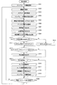
始めに、図1を用いて、本実施の形態に係るA/D変換装置の構成について説明する。図1は、実施の形態1に係るA/D変換装置の構成を示すブロック図である。本実施の形態に係るA/D変換装置は、コンパレータ機能とA/D変換機能の切り替えが可能なものである。すなわち、互いに切り替え可能なコンパレータ機能とA/D変換機能とを有している。
Embodiment 1 FIG.
First, the configuration of the A / D conversion device according to the present embodiment will be described with reference to FIG. FIG. 1 is a block diagram illustrating a configuration of an A / D conversion apparatus according to the first embodiment. The A / D conversion device according to this embodiment can switch between the comparator function and the A / D conversion function. That is, it has a comparator function and an A / D conversion function that can be switched to each other.
本実施の形態のA/D変換装置は、制御回路11、比較結果カウンタ12、比較器13、サンプルホールド回路14、逐次変換レジスタ15、変換結果レジスタ16、D/A変換器17、及び基準電源18を備えている。
The A / D converter according to the present embodiment includes a
制御回路11は、動作の開始指示23、比較判定用のカウント値24、閾値25、及びクロック入力21を入力とする。制御回路11は、入力された閾値25に対応するデジタル値を逐次変換レジスタ15に出力する。また、制御回路11は、入力されたカウント値24を比較結果カウンタ12に設定する。
The
サンプルホールド回路14は、アナログ入力Vin20を入力とする。サンプルホールド回路14は、コンパレータ機能動作時には、入力されたアナログ入力Vin20のサンプリング処理を行い、電圧を保持する。サンプルホールド回路14の出力は、比較器13のマイナス入力端子に接続されている。なお、サンプルホールド回路14は、コンパレータ機能動作開始時にサンプリング処理を行い、サンプリング処理後のA/D変換機能動作時には再サンプリング処理を行わない。
The
D/A変換器17には、基準電源18から基準電圧が供給され、逐次変換レジスタ15が保存するデジタル値をアナログ値に変換する。具体的には、D/A変換器17は、基準電源18から供給される基準電圧を用いて、逐次変換レジスタ15から与えられるデジタル値に応じたアナログ電圧を生成している。D/A変換器17の出力は、比較器13のプラス入力端子に接続されている。
The D / A converter 17 is supplied with a reference voltage from the
比較器13は、入力端子に与えられた電圧を比較し、その比較結果を出力する。すなわち、比較器13は、サンプルホールド回路14が出力するアナログ電圧と、D/A変換器17から得られるアナログ電圧との比較を行う。比較器13の出力は、逐次変換レジスタ15と比較結果カウンタ12とに接続されている。
The
比較結果カウンタ12は、比較器13から入力される比較結果に応じてカウントを行い、そのカウント数に応じて判定結果を出力する。具体的には、比較結果カウンタ12は、比較器13から入力される比較結果が直前の比較結果と一致する場合はカウントし、一致しない場合はカウンタを0にクリアする。そして、カウンタのカウント数が設定されたカウント値24以上であるか否かを判定し、その判定結果22を出力する。比較結果カウンタ12は、判定結果22を制御回路11に出力する。また、比較結果カウンタ12は、判定結果22を外部に出力してもよい。
The comparison result counter 12 counts according to the comparison result input from the
制御回路11は、コンパレータ機能を連続動作させるコンパレータ制御回路(不図示)と、コンパレータ機能動作時における比較結果に応じてA/D変換機能の動作を開始させるA/D変換制御回路(不図示)とを有している。制御回路11は、比較結果カウンタ12から入力される判定結果22を開始トリガとして、コンパレータ機能からA/D変換機能へ移行するための制御を行う。また、制御回路11は、A/D変換終了後、変換終了信号であるINT16を出力する。
The
逐次変換レジスタ15は、制御回路11から入力された、閾値25に対応するデジタル値を保存する。また、A/D変換機能動作時には、逐次変換レジスタ15は、比較器13から出力される比較結果を保持し、A/D変換を実行する。具体的には、逐次変換レジスタ15は、サンプルホールド回路14にて保持されたアナログ電圧を逐次変換する。すなわち、コンパレータ機能からA/D変換機能への切り替え時には、サンプルホールド回路14に蓄えられたアナログ入力Vin20の電圧をそのまま使用してA/D変換を行う。そして、逐次変換レジスタ15は、変換したデジタル値を変換結果レジスタ16へ出力する。
The successive approximation register 15 stores a digital value input from the
変換結果レジスタ16は、逐次変換レジスタ15から入力されたA/D変換後のデジタル値を保持し、A/D変換結果27として出力する。
The
続いて、本実施の形態に係るA/D変換装置の制御方法について、図2を用いて説明する。図2は、実施の形態1に係るA/D変換装置の制御の流れを示すフローチャートである。 Subsequently, a control method of the A / D conversion device according to the present embodiment will be described with reference to FIG. FIG. 2 is a flowchart showing a control flow of the A / D conversion device according to the first embodiment.
図2に示すように、制御回路11は、A/D変換装置が起動されると、コンパレータ機能を選択する(S201)。次に、制御回路11に対して、コンパレータ機能で使用する閾値25を設定する(S202)。また、制御回路11に対して、カウント値24を入力し、比較判定用のカウント数を設定する(S203)。すなわち、制御回路11は、入力されたカウント値24を比較結果カウンタ12に設定する。
As shown in FIG. 2, when the A / D converter is activated, the
コンパレータ機能を開始するための開始指示23が制御回路11に入力されると、A/D変換装置はコンパレータ機能の動作を開始する(S204)。制御回路11は、設定された閾値25に対応するデジタル値を逐次変換レジスタ15に出力し(S205)、逐次変換レジスタ15がこれを保持する。
When the
次に、サンプルホールド回路14は、アナログ入力Vin20から供給されるアナログ電圧を取り込み、取り込んだアナログ電圧を保持する(S206)。そして、サンプルホールド回路14は、保持したアナログ電圧(保持電圧)を比較器13に出力する(S207)。一方、D/A変換器17は、基準電源18から供給される基準電圧と、逐次変換レジスタ15から入力されるデジタルデータとに基づいて、比較用のアナログ電圧(比較用電圧)を比較器13に出力する(S208)。ここでは、比較用電圧として、閾値25に応じたアナログ電圧が出力される。
Next, the
比較器13は、サンプルホールド回路14から入力されるアナログ電圧(保持電圧)と、D/A変換器17から入力される比較判定用の閾値25に対応するアナログ電圧(比較用電圧)とを比較し(S209)、その比較結果を出力する。例えば、図3に示すように、サンプルホールド回路14から入力される保持電圧が、D/A変換器17から入力される比較用電圧よりも高い場合にはHigh、低い場合にはLowを比較結果として出力する。このようにして、コンパレータ判定を行う。
The
比較結果カウンタ12は、比較器13が出力する比較結果が直前の比較結果と一致するか否かの判定を行う(S210)。すなわち、比較器13の出力信号が前回の比較器13の出力信号と同じかどうか判定する。一致する場合はカウントし、カウンタをインクリメントする(S211)。一致しない場合はカウンタのカウント数を0にクリアする(S212)。
The comparison result
続いて、比較結果カウンタ12は、カウンタのカウント数が制御回路11から設定されたカウント値24以上であるか否かを判定する(S213)。カウント数が設定されたカウント値24以上の場合は、カウント条件に適合したとみなし、比較結果カウンタ12は、Highを判定結果22として出力する(S214)。なお、カウント数が設定されたカウント値24数未満の場合は、Lowを出力する。
Subsequently, the
次に、制御回路11は、比較結果カウンタ12から入力される判定結果22が"H"(High)であるか否かの判定を行う(S215)。
Next, the
S215の判定において判定結果22が"H"の場合は、A/D変換機能へ切り替えを行う。すなわち、制御回路11は、比較結果カウンタ12から入力される判定結果22をトリガとして、コンパレータ機能からA/D変換機能へ移行するための制御を行う。このように、本実施の形態では、A/D変換機能が、コンパレータ機能動作の判定結果に連動して開始される。そして、A/D変換を実行する(S216)。ここでは、サンプルホールド回路14にて保持されたアナログ電圧をデジタル値に変換するA/D変換処理が、逐次変換レジスタ15によって行われる。このとき、コンパレータ動作で閾値に設定した値から逐次変換型のA/D変換の検出方法であるバイナリーサーチを開始する。これにより、バイナリーサーチの回数を少なくすることができ、A/Dの変換処理期間を短縮できる。なお、このA/D変換処理期間の間、サンプルホールド回路14は、アナログ入力Vin20から供給されるアナログ電圧を取り込む再サンプリング動作は行わない。
When the
A/D変換処理完了後、逐次変換レジスタ15は変換したデジタル値を出力する。変換結果レジスタ16は、逐次変換レジスタ15から入力されたA/D変換後のデジタル値を保持し、A/D変換結果27として出力する(S217)。また、制御回路11は、変換終了信号であるINT26を出力し(S218)、コンパレータ機能を選択する(S219)。すなわち、A/D変換処理が完了後、制御回路11は、コンパレータ機能動作を再実行させる。
After completing the A / D conversion process, the successive approximation register 15 outputs the converted digital value. The
その後、閾値・カウント数の変更がなされたかどうかの判定を行う(S220)。閾値25の設定値、比較結果カウンタ12のカウント数を変更して動作を継続する場合はS202へ戻り、現状設定での動作を継続する場合はS205へ戻る。なお、S215の判定において判定結果22が"H"でない場合は、S216〜S219を経由しないでS220へと移行する。すなわち、A/D変換機能への切り替えは行われず、コンパレータ機能動作が継続される。
Thereafter, it is determined whether or not the threshold value / count number has been changed (S220). If the setting value of the
次に、以上のように構成された本実施の形態に係るA/D変換装置の動作について、図3を用いて説明する。図3は、本実施の形態に係るA/D変換装置の動作を示すタイミングチャートである。以下では、適宜、特許文献1に開示された従来のA/D変換装置の動作と比較しながら説明を行う。 Next, the operation of the A / D converter according to the present embodiment configured as described above will be described with reference to FIG. FIG. 3 is a timing chart showing the operation of the A / D converter according to the present embodiment. The following description will be made while comparing with the operation of the conventional A / D converter disclosed in Patent Document 1 as appropriate.
図3に示すように、本実施の形態では、コンパレータ機能動作の開始指示23が入力されると、コンパレータ動作の連続実行を自動的に行う。すなわち、所定のタイミングでコンパレータ判定が継続的に行われる。このコンパレータ動作は、コンパレータ判定が所定のカウント条件に適合するまで継続的に行われる。そして、コンパレータ判定が所定のカウント条件に適合すると、コンパレータ機能からA/D変換機能へ移行される。具体的には、上述したように、比較結果カウンタ12が判定結果22としてHighを出力し、この出力を起動トリガとしてA/D変換処理がスタートする。なお、A/D変換処理期間は、コンパレータ判定を行わない不定状態となる。A/D変換処理が終了すると、A/D変換結果27が出力されるとともに、変換終了信号であるINT26が出力されてコンパレータ動作が再実行される。
As shown in FIG. 3, in the present embodiment, when a comparator function operation start
ここで、従来のA/D変換装置では、図6のタイミングチャートに示したように、コンパレータ動作の判定結果が出た後、マイクロコンピュータ106が判定結果を読み取り、A/D変換機能の開始命令を出している。すなわち、コンパレータ動作の連続実行と、コンパレータ機能からA/D変換機能への切り替えとをマイクロコンピュータ106によるソフトウェア処理で行っている。そのため、コンパレータ動作が完了する毎にマイクロコンピュータ106の判断を待つ待機時間が生じ、コンパレータ動作の再実行やコンパレータ機能からA/D変換機能への切り替え処理に長い時間を要する。また、この待機期間にアナログ入力Vinは刻々と変化するため、コンパレータ動作の判定結果とA/Dの変換結果が一致しない。
Here, in the conventional A / D conversion apparatus, as shown in the timing chart of FIG. 6, after the determination result of the comparator operation is output, the
これに対して、本実施の形態では、連続動作を可能とするコンパレータ制御回路を制御回路11に設けたことで、コンパレータ機能動作の開始指示23が入力された後は、コンパレータ動作の連続実行を自動的に行うことができる。すなわち、図3に示すように、コンパレータ動作の判定結果後、ソフトウェア処理を行うことなく直ちに次のコンパレータ動作を開始できるため、動作開始指示待ちの待機状態は無い。従って、本実施の形態のA/D変換装置は、コンパレータ動作の再実行処理に要する時間を従来のA/D変換装置よりも短縮できる。
On the other hand, in this embodiment, the comparator control circuit that enables continuous operation is provided in the
また、本実施の形態では、コンパレータ動作の比較結果を起動トリガとするA/D変換制御回路を制御回路11に設けたことで、コンパレータ動作の判定結果に連動してA/D変換を開始できる。すなわち、図3に示すように、コンパレータ動作の判定結果後、ソフトウェア処理を行うことなく直ちにA/D変換を開始できるため、動作開始指示待ちの待機状態は無い。従って、本実施の形態のA/D変換装置は、コンパレータ機能からA/D変換機能への切り替え処理に要する時間を従来のA/D変換装置よりも短縮できる。
In the present embodiment, the A / D conversion control circuit using the comparison result of the comparator operation as a start trigger is provided in the
さらに、本実施の形態では、コンパレータ動作で使用したアナログ入力Vin20をそのままA/Dの変換の入力としても使用する。そのため、コンパレータ動作の判定結果とA/Dの変換結果が一致する。通常、アナログ入力Vinは、閾値近辺で閾値を超えたり超えなかったりという変動をする。従来のA/D変換装置では、ほんのわずかでも閾値を超えたときにコンパレータ動作を行っていた場合A/D変換機能の開始命令を出すが、待機状態中にアナログ入力Vinが変化し閾値を超えていない状態でA/D変換を行うことがあり、A/D変換時間の無駄が生じる。また、本実施の形態では、比較結果カウンタ12を設けたことで、アナログ入力Vin20が閾値25から確実に超えた時点でA/D変換動作を行うことができる。すなわち、アナログ入力Vin20にノイズが乗った場合においてもノイズを特定範囲と誤判断することなく再度コンパレータ動作を実行し、アナログ入力Vin20が特定範囲に入っているかどうか判定を行う。このように、ノイズによるアナログ入力Vin20の異常変動や閾値近傍の判定ブレを防止するデジタルノイズフィルターの機能を実現することができる。従って、誤判定などによるA/D変換時間の無駄が生じない。
Furthermore, in this embodiment, the
以上のように、本実施の形態のA/D変換装置では、コンパレータ動作の連続実行と、コンパレータ機能からA/D変換機能への切り替えとを、マイクロコンピュータによるソフトウェア処理なしで行う。これにより、コンパレータ動作の再実行やコンパレータ機能からA/D変換機能への切り替え処理に要する時間を短縮することができる。また、コンパレータ機能からA/D変換機能へ移行を、コンパレータ判定が所定のカウント条件に適合したときに行う。これにより、ノイズなどの誤判定によって、A/D変換時間の無駄が生じることを防止できる。さらに、A/D変換処理時には、サンプルホールド回路14に蓄えたアナログ入力Vin20電圧をそのまま使用する。これにより、A/D変換結果がコンパレータ判定結果と一致し、A/D変換時間の無駄が生じることを防止できる。また、コンパレータ動作で閾値に設定した値から逐次変換型のA/D変換の検出方法であるバイナリーサーチを開始する。これにより、A/Dの変換処理時間を短縮できる。従って、本実施の形態によれば、処理時間を効果的に短縮できるA/D変換装置を提供することができる。
As described above, in the A / D conversion device of the present embodiment, continuous execution of the comparator operation and switching from the comparator function to the A / D conversion function are performed without software processing by the microcomputer. As a result, the time required for re-execution of the comparator operation and switching processing from the comparator function to the A / D conversion function can be shortened. In addition, the shift from the comparator function to the A / D conversion function is performed when the comparator determination conforms to a predetermined count condition. Thereby, it is possible to prevent waste of A / D conversion time due to erroneous determination such as noise. Further, during the A / D conversion process, the
実施の形態2.
本実施の形態に係るA/D変換装置の構成について、図4を用いて説明する。図4は、実施の形態2に係るA/D変換装置の構成を示すブロック図である。
Embodiment 2. FIG.
The configuration of the A / D conversion device according to this embodiment will be described with reference to FIG. FIG. 4 is a block diagram showing a configuration of the A / D conversion apparatus according to the second embodiment.
実施の形態1では、アナログ入力Vin20が特定の電圧以上、または特定の電圧以下のときにコンパレータ機能からA/D変換機能に移行させる場合に本発明のA/D変換装置を適用する例について説明をしたが、本実施の形態では、アナログ入力Vin20が特定の電圧範囲内のときにコンパレータ機能からA/D変換機能に移行させる場合に本発明のA/D変換装置を適用する例について説明をする。
In the first embodiment, when the
実施の形態1では、制御回路11は、1つの閾値25を入力としていたが、本実施の形態では、2つの閾値25を入力とする。具体的には、図4に示すように、第1閾値25aと第2閾値25bとが制御回路11に入力される。例えば、制御回路11は、第1閾値25aと第2閾値25bとを保持する格納レジスタ(不図示)をさらに有している。制御回路11は、入力された第1閾値25aと第2閾値25bにそれぞれ対応するデジタル値を逐次変換レジスタ15に対して交互に出力する。
In the first embodiment, the
逐次変換レジスタ15及び比較器13は、第1閾値25aと第2閾値25bの2つ分の閾値25の処理を行う。すなわち、逐次変換レジスタ15は、第1閾値25aと第2閾値25bにそれぞれ対応するデジタル値を交互に保存する。そして、比較器13は、サンプルホールド回路14が出力するアナログ電圧を、逐次変換レジスタ15が出力する第1閾値25aと第2閾値25bのそれぞれと比較する。
The
また、比較結果カウンタ12は、カウントレジスタを2回設定する制御を有している。すなわち、比較器13が出力する、第1閾値25aに対応する比較結果と第2閾値25bに対応する比較結果との両方に基づいてカウントされたカウント数に応じて判定結果22を出力する。例えば、第1閾値25a<第2閾値25bの場合、比較結果カウンタ12は、比較器13の第1閾値25aに対応する比較結果がHighならカウントを行い、Lowならばクリアを行う。続いて、比較器13の第2閾値25bに対応する比較結果がHighならクリアを行い、Lowならカウントを行う。そして、比較結果カウンタ12は、カウンタが設定されたカウント数以上であるか否かを判定し、その判定結果22を出力する。それ以外の構成については、実施の形態1と同様であるため、説明を省略する。
The comparison result
次に、本実施の形態に係るA/D変換装置の制御方法について説明する。ここでは、図2に示す実施の形態1のフローチャートと同じ部分については説明を省略し、差異について説明する。 Next, a method for controlling the A / D conversion device according to the present embodiment will be described. Here, the description of the same part as the flowchart of the first embodiment shown in FIG. 2 is omitted, and the difference will be described.
本実施の形態では、S202において、第1閾値25aと第2閾値25bとを制御回路11に対して設定する。そして、S205において、制御回路11は設定された第1閾値25aと第2閾値25bにそれぞれ対応するデジタル値を逐次変換レジスタ15に出力する。また、S208からS212までのフローを2回繰り返して行う。例えば、1回目は第1閾値25aの値を使用して行い、2回目は第2閾値25aの値を使用して行う。このとき、S210では、例えば第1閾値25a<第2閾値25bとすると、1回目の比較結果がHighならカウントを行い、Lowならばクリアを行う。続く2回目の比較結果がHighならクリアを行い、Lowならカウントを行う。
In the present embodiment, the
このようにして、サンプルホールド回路14が出力するアナログ電圧が、第1閾値25aと第2閾値25bの間の電圧範囲にあるときに、比較結果カウンタ12のカウントが行われる。これにより、アナログ入力Vin20が特定の電圧範囲内のときにA/D変換機能を実行させることができる。例えば、アナログ入力Vin20が0Vから5Vまでをとる場合、第1閾値25aを2V、第2閾値25bを3Vに設定すると、2Vから3Vまでの範囲内に電圧が収まっていたときにA/D変換機能が実行されるようになる。
In this way, the comparison result counter 12 counts when the analog voltage output from the sample and hold
以上のように、本実施の形態では、第1閾値25a及び第2閾値25b用の格納レジスタを制御回路11に設け、比較結果カウンタ12内のカウントレジスタを2回設定する。これにより、コンパレータ動作の判定のための閾値25を上下に設定でき、実施の形態1と同様に無駄の無い動作によって、希望する領域内だけのA/D変換値取得が可能となる。このように閾値25を2つ設けることで、希望する領域のより限定した範囲内だけのA/D変換結果が求められる場合において、処理時間の短縮ができる。また、実施の形態1と同様の効果を奏することができる。
As described above, in the present embodiment, the storage registers for the
なお、本発明は上記実施の形態に限られたものではなく、趣旨を逸脱しない範囲で適宜変更することが可能である。例えば、実施の形態2では、アナログ入力Vin20が特定の電圧範囲内のときにコンパレータ機能からA/D変換機能に移行させる場合について説明を行ったが、特定の電圧範囲外のときにコンパレータ機能からA/D変換機能に移行させてもよい。
Note that the present invention is not limited to the above-described embodiment, and can be changed as appropriate without departing from the spirit of the present invention. For example, in the second embodiment, the case where the
11 制御回路、12 比較結果カウンタ、
13 比較器、14 サンプルホールド回路、
15 逐次変換レジスタ、16 変換結果レジスタ、
17 D/A変換器、18 基準電源、
20 アナログ入力Vin、21 クロック入力、
22 判定結果、23 開始指示、
24 カウント値、25 閾値、
25a 第1閾値、25b 第2閾値、
26 INT、27 A/D変換結果、
106 マイクロコンピュータ、
107 シフトレジスタ、108 保持レジスタ、
109 3出力(3状態)バッファ、
110 D/A変換器、111 基準電源、
112 比較器
11 control circuit, 12 comparison result counter,
13 comparator, 14 sample hold circuit,
15 successive conversion registers, 16 conversion result registers,
17 D / A converter, 18 reference power supply,
20 analog input V in, 21 clock input,
22 judgment result, 23 start instruction,
24 count value, 25 threshold value,
25a first threshold, 25b second threshold,
26 INT, 27 A / D conversion result,
106 microcomputer,
107 shift register, 108 holding register,
109 3 output (3 state) buffer,
110 D / A converter, 111 reference power supply,
112 comparator
Claims (10)
入力された入力アナログ電圧を保持するサンプルホールド回路と、
前記コンパレータ機能における比較判定用の閾値に対応するデジタル値を保存する逐次変換レジスタと、
前記逐次変換レジスタが保存するデジタル値に応じたアナログ電圧を生成するD/A変換器と、
前記サンプルホールド回路が出力するアナログ電圧と、前記D/A変換器から得られるアナログ電圧とを比較し比較結果を出力する比較器と、
前記比較結果に基づいてカウントされたカウント数に応じて判定結果を出力する比較結果カウンタと、
前記判定結果に基づいて、前記コンパレータ機能から前記A/D変換機能へ移行するための制御を行う制御回路と、を備え、
前記逐次変換レジスタは、前記A/D変換機能動作時には、前記サンプルホールド回路にて保持されたアナログ電圧をデジタル値に逐次変換するA/D変換処理を行うA/D変換装置。 An A / D conversion device capable of switching between a comparator function and an A / D conversion function,
A sample-and-hold circuit that holds the input analog voltage, and
A successive approximation register for storing a digital value corresponding to a threshold value for comparison determination in the comparator function;
A D / A converter that generates an analog voltage corresponding to a digital value stored in the successive approximation register;
A comparator that compares the analog voltage output by the sample and hold circuit with the analog voltage obtained from the D / A converter and outputs a comparison result;
A comparison result counter that outputs a determination result according to a count number counted based on the comparison result;
A control circuit that performs control for shifting from the comparator function to the A / D conversion function based on the determination result;
The successive approximation register is an A / D conversion device that performs A / D conversion processing for sequentially converting the analog voltage held by the sample hold circuit into a digital value when the A / D conversion function is operated.
前記コンパレータ機能を連続動作させるコンパレータ制御回路と、
前記コンパレータ機能動作時における前記比較結果に応じて前記A/D変換機能の動作を開始させるA/D変換制御回路と、を有する請求項1又は2に記載のA/D変換装置。 The control circuit includes:
A comparator control circuit for continuously operating the comparator function;
The A / D conversion device according to claim 1, further comprising: an A / D conversion control circuit that starts an operation of the A / D conversion function according to the comparison result during the comparator function operation.
前記コンパレータ機能動作時には、前記入力アナログ電圧のサンプリング処理を行い、
前記A/D変換機能動作時には、前記入力アナログ電圧のサンプリング処理を行わない請求項1乃至3のいずれか1項に記載のA/D変換装置。 The sample and hold circuit includes:
When the comparator function operates, the input analog voltage is sampled,
4. The A / D conversion device according to claim 1, wherein sampling processing of the input analog voltage is not performed during the A / D conversion function operation. 5.
前記比較結果カウンタは、前記比較器が出力する、前記第1閾値に対応する前記比較結果と、前記第2閾値に対応する前記比較結果との両方に基づいてカウントされたカウント数に応じて前記判定結果を出力する請求項1乃至8のいずれか1項に記載のA/D変換装置。 The successive approximation register alternately stores digital values corresponding to the first threshold value and the second threshold value,
The comparison result counter is configured to output the comparator in accordance with a count number counted based on both the comparison result corresponding to the first threshold value and the comparison result corresponding to the second threshold value. The A / D converter according to any one of claims 1 to 8, which outputs a determination result.
Priority Applications (3)
| Application Number | Priority Date | Filing Date | Title |
|---|---|---|---|
| JP2009116789A JP2010268139A (en) | 2009-05-13 | 2009-05-13 | A/d converter |
| KR1020100031327A KR101138390B1 (en) | 2009-05-13 | 2010-04-06 | A/d conversion device |
| US12/755,902 US8115664B2 (en) | 2009-05-13 | 2010-04-07 | A/D conversion device |
Applications Claiming Priority (1)
| Application Number | Priority Date | Filing Date | Title |
|---|---|---|---|
| JP2009116789A JP2010268139A (en) | 2009-05-13 | 2009-05-13 | A/d converter |
Publications (2)
| Publication Number | Publication Date |
|---|---|
| JP2010268139A true JP2010268139A (en) | 2010-11-25 |
| JP2010268139A5 JP2010268139A5 (en) | 2012-04-05 |
Family
ID=43068078
Family Applications (1)
| Application Number | Title | Priority Date | Filing Date |
|---|---|---|---|
| JP2009116789A Pending JP2010268139A (en) | 2009-05-13 | 2009-05-13 | A/d converter |
Country Status (3)
| Country | Link |
|---|---|
| US (1) | US8115664B2 (en) |
| JP (1) | JP2010268139A (en) |
| KR (1) | KR101138390B1 (en) |
Cited By (1)
| Publication number | Priority date | Publication date | Assignee | Title |
|---|---|---|---|---|
| US8502724B2 (en) | 2011-04-01 | 2013-08-06 | Semiconductor Energy Laboratory Co., Ltd. | Semiconductor device and method for driving the same |
Families Citing this family (4)
| Publication number | Priority date | Publication date | Assignee | Title |
|---|---|---|---|---|
| US8344924B2 (en) * | 2010-04-27 | 2013-01-01 | Analog Devices, Inc. | Analog signal conversion |
| KR101749571B1 (en) * | 2010-12-13 | 2017-06-22 | 삼성전자주식회사 | Motor control system |
| GB2532972B (en) * | 2014-12-03 | 2021-03-10 | Atlantic Inertial Systems Ltd | Successive approximation ADC |
| TWI594579B (en) * | 2016-06-13 | 2017-08-01 | 瑞昱半導體股份有限公司 | Successive approximation register analog to digital converter and analog to digital conversion method thereof |
Citations (5)
| Publication number | Priority date | Publication date | Assignee | Title |
|---|---|---|---|---|
| JPS61125231A (en) * | 1984-11-21 | 1986-06-12 | Canon Inc | Analog-digital converter |
| JPH0465918A (en) * | 1990-07-02 | 1992-03-02 | Fujitsu Ltd | Successive comparison ad converter |
| JPH06152421A (en) * | 1992-11-13 | 1994-05-31 | Nec Corp | A/d converter |
| JPH0784654A (en) * | 1993-09-14 | 1995-03-31 | Sony Tektronix Corp | Power control circuit |
| JPH10303751A (en) * | 1997-04-22 | 1998-11-13 | Miyagi Oki Denki Kk | Analog/digital converter |
Family Cites Families (8)
| Publication number | Priority date | Publication date | Assignee | Title |
|---|---|---|---|---|
| US3153142A (en) * | 1960-12-30 | 1964-10-13 | Ibm | Monitor-converter system |
| US4112500A (en) * | 1976-01-19 | 1978-09-05 | The Singer Company | Smoothing of updated digital data |
| JPS55100741A (en) * | 1979-01-26 | 1980-07-31 | Hitachi Ltd | Multi-input comparator |
| JPS5952576B2 (en) | 1979-07-13 | 1984-12-20 | 株式会社東芝 | A/D converter stabilization circuit |
| JPH01161922A (en) * | 1987-12-17 | 1989-06-26 | Mitsubishi Electric Corp | Analog-digital converter |
| JP2004032415A (en) | 2002-06-26 | 2004-01-29 | Nec Micro Systems Ltd | Analog-to-digital converter |
| US7405689B2 (en) | 2005-01-05 | 2008-07-29 | Exar Corporation | Predictive analog to digital converters and methods of using |
| US8004442B2 (en) * | 2009-04-23 | 2011-08-23 | Infineon Technologies Ag | Analog to digital converter (ADC) with comparator function for analog signals |
-
2009
- 2009-05-13 JP JP2009116789A patent/JP2010268139A/en active Pending
-
2010
- 2010-04-06 KR KR1020100031327A patent/KR101138390B1/en not_active IP Right Cessation
- 2010-04-07 US US12/755,902 patent/US8115664B2/en not_active Expired - Fee Related
Patent Citations (5)
| Publication number | Priority date | Publication date | Assignee | Title |
|---|---|---|---|---|
| JPS61125231A (en) * | 1984-11-21 | 1986-06-12 | Canon Inc | Analog-digital converter |
| JPH0465918A (en) * | 1990-07-02 | 1992-03-02 | Fujitsu Ltd | Successive comparison ad converter |
| JPH06152421A (en) * | 1992-11-13 | 1994-05-31 | Nec Corp | A/d converter |
| JPH0784654A (en) * | 1993-09-14 | 1995-03-31 | Sony Tektronix Corp | Power control circuit |
| JPH10303751A (en) * | 1997-04-22 | 1998-11-13 | Miyagi Oki Denki Kk | Analog/digital converter |
Cited By (1)
| Publication number | Priority date | Publication date | Assignee | Title |
|---|---|---|---|---|
| US8502724B2 (en) | 2011-04-01 | 2013-08-06 | Semiconductor Energy Laboratory Co., Ltd. | Semiconductor device and method for driving the same |
Also Published As
| Publication number | Publication date |
|---|---|
| KR101138390B1 (en) | 2012-04-26 |
| KR20100122853A (en) | 2010-11-23 |
| US8115664B2 (en) | 2012-02-14 |
| US20100289681A1 (en) | 2010-11-18 |
Similar Documents
| Publication | Publication Date | Title |
|---|---|---|
| US10044364B1 (en) | Metastability error correction methods and circuits for asynchronous successive approximation analog to digital converter (SAR ADC) | |
| US8957802B1 (en) | Metastability error detection and correction system and method for successive approximation analog-to-digital converters | |
| JP5169486B2 (en) | FPGA configuration device, circuit board having the same, electronic device, and FPGA configuration method | |
| TWI572143B (en) | Successive approximation register (sar) analog- to-digital converter (adc) circuit and method thereof | |
| JP2010268139A (en) | A/d converter | |
| JP5277248B2 (en) | AD converter | |
| US10700594B2 (en) | Power conversion device | |
| US10116318B1 (en) | Method and system for asynchronous clock generation for successive approximation analog-to-digital converter (SAR ADC) | |
| JPWO2010010660A1 (en) | AD converter | |
| EP2842230A1 (en) | Method and apparatus for analog-to-digital converter | |
| JP2010093538A (en) | Ad conversion device and method for detecting failure of ad conversion device | |
| US9342097B2 (en) | Microcontroller and method of controlling the same | |
| JP2011077847A (en) | A/d converter and open detection method thereof | |
| JP4181058B2 (en) | Analog / digital converter and microcomputer equipped with the same | |
| JP7251335B2 (en) | GATE DRIVE DEVICE, SWITCHING DEVICE, AND GATE DRIVE METHOD | |
| CN111464165A (en) | SOC power supply power-on and power-off time sequence control method | |
| JP2018045583A (en) | Signal processing device | |
| US8729943B2 (en) | Phase interpolating apparatus and method | |
| US8502722B2 (en) | Analog to digital converting apparatus and method thereof | |
| WO2017094765A1 (en) | Switch failure diagnosis device | |
| JP2007281695A (en) | Analog/digital converter | |
| JP2017207382A (en) | Electronic controller | |
| JP2005348095A (en) | A/d converter and a/d conversion method | |
| CN113078907B (en) | Multi-stage switched capacitor circuit and method of operation thereof | |
| JPH08293791A (en) | Analog/digital converter |
Legal Events
| Date | Code | Title | Description |
|---|---|---|---|
| A521 | Written amendment |
Free format text: JAPANESE INTERMEDIATE CODE: A523 Effective date: 20120220 |
|
| A621 | Written request for application examination |
Free format text: JAPANESE INTERMEDIATE CODE: A621 Effective date: 20120220 |
|
| A977 | Report on retrieval |
Free format text: JAPANESE INTERMEDIATE CODE: A971007 Effective date: 20130514 |
|
| A131 | Notification of reasons for refusal |
Free format text: JAPANESE INTERMEDIATE CODE: A131 Effective date: 20130521 |
|
| A02 | Decision of refusal |
Free format text: JAPANESE INTERMEDIATE CODE: A02 Effective date: 20130924 |