JP2010256552A - Optical circuit element - Google Patents
Optical circuit element Download PDFInfo
- Publication number
- JP2010256552A JP2010256552A JP2009105272A JP2009105272A JP2010256552A JP 2010256552 A JP2010256552 A JP 2010256552A JP 2009105272 A JP2009105272 A JP 2009105272A JP 2009105272 A JP2009105272 A JP 2009105272A JP 2010256552 A JP2010256552 A JP 2010256552A
- Authority
- JP
- Japan
- Prior art keywords
- core
- optical
- circuit element
- clad
- optical circuit
- Prior art date
- Legal status (The legal status is an assumption and is not a legal conclusion. Google has not performed a legal analysis and makes no representation as to the accuracy of the status listed.)
- Pending
Links
Images


Abstract
Description
本発明は光回路素子に関するものであり、特に、光強度や光位相等の調整に用いられる光回路素子に関するものである。 The present invention relates to an optical circuit element, and more particularly to an optical circuit element used for adjusting light intensity, optical phase, and the like.
光回路素子のうち、例えば、マッハツェンダー干渉計(Mach-Zehnder Interferometer)型の光スイッチ(以下、「MZI型光スイッチ」と称する。)は、光回路の空間切り替えに広く用いられている。一般的なMZI型光スイッチは、熱光学効果(熱による屈折率の変化)を利用して導波路を伝搬する光のスイッチングを行う。かかるMZI型光スイッチの基本構造を図4に模式的に示す。一般的なMZI型光スイッチでは、基板101の上に、クラッド102とコア103とからなる光位相シフト導波路104が形成されている。さらに、光位相シフト導波路104のクラッド102上にはヒーター105が設けられている。図示されているような構造のMZI型光スイッチでは、ヒーター105の加熱により光位相シフト導波路104の屈折率を変えることよって、該導波路104を伝搬する光の位相をシフトさせる。これにより、加熱された光位相シフト導波路と不図示のもう一方の光位相シフト導波路との共同作用によって光がスイッチングされる。
Among optical circuit elements, for example, a Mach-Zehnder Interferometer type optical switch (hereinafter, referred to as “MZI type optical switch”) is widely used for spatial switching of optical circuits. A general MZI type optical switch performs switching of light propagating through a waveguide using a thermo-optic effect (change in refractive index due to heat). The basic structure of such an MZI type optical switch is schematically shown in FIG. In a general MZI type optical switch, an optical
しかし、図4に示されているヒーター105から発せられた熱は、クラッド102の内部で発散しながら伝導する。さらに、クラッド102の下方の基板101にも伝導する。このため、コア103を効率よく加熱することができず、スイッチングに必要な消費電力が大きく、スイッチングの応答速度も低いといった課題があった。 However, the heat generated from the heater 105 shown in FIG. 4 is conducted while being dissipated inside the clad 102. Further, it is also conducted to the substrate 101 below the clad 102. For this reason, the core 103 cannot be efficiently heated, and there is a problem that power consumption necessary for switching is large and switching response speed is low.
上記課題を解決するための構造として図5に示す構造が知られている。図5に示す構造では、光位相シフト導波路104の周囲に空隙(断熱部106)が設けられている。しかし、図5に示す構造には、断熱部106を形成するためのデバイス加工プロセスが複雑になるという課題があった。また、デバイスの機械的強度や信頼性が低いといった課題もあった。
A structure shown in FIG. 5 is known as a structure for solving the above problem. In the structure shown in FIG. 5, a gap (heat insulating portion 106) is provided around the optical
そこで、特許文献1には、図6に示す構造のMZI型光スイッチが記載されている。図6に示すMZI型光スイッチでは、ヒーター105とコア103との間に、繊維強化複合材料107とバッファ層108とが配置されている。繊維強化複合材料107は、異方性を有し、かつ、一方向にのみ高い熱伝導率を有する。バッファ層108は、繊維強化複合材料107による光吸収を防ぐために配置されている。
Therefore,
特許文献1に開示されている構造では、繊維強化複合材料による光吸収を防ぐためにバッファ層が設けられている。しかし、バッファ層は、一般的に熱伝導率が低い。したがって、ヒーターとコアとの間の熱伝導効率の向上と、光吸収の抑制といった2つの目的が十分には達成されない。
In the structure disclosed in
本発明は上記課題に鑑みてなされたものであり、その目的は、加熱素子または冷却素子とコアとの間の熱伝導効率の向上と、光吸収の抑制といった2つの目的が十分に達成された光回路素子を提供することである。 The present invention has been made in view of the above-mentioned problems, and its purpose has been sufficiently achieved by the two purposes of improving the heat conduction efficiency between the heating element or the cooling element and the core and suppressing light absorption. An optical circuit element is provided.
本発明の光回路素子は、熱光学効果によって光導波路を伝搬する光の位相を変化させる光回路素子であって、クラッドと該クラッドによって覆われたコアとからなる光導波路と、加熱素子または冷却素子と、前記クラッド内に埋設され、前記加熱素子または前記冷却素子と前記コアとを熱的に接続する伝熱部材としてのカーボンナノチューブとを有することを特徴とする。 An optical circuit element of the present invention is an optical circuit element that changes the phase of light propagating through an optical waveguide by a thermooptic effect, and includes an optical waveguide composed of a clad and a core covered by the clad, and a heating element or a cooling element. It has an element and the carbon nanotube as a heat-transfer member embedded in the said clad and thermally connecting the said heating element or the said cooling element, and the said core.
本発明によれば、加熱素子または冷却素子とコアとの間の熱伝導効率の向上と、光吸収や光損失の抑制といった2つの目的が十分に達成された光回路素子が実現される。 According to the present invention, an optical circuit element is realized in which two purposes such as improvement of heat conduction efficiency between a heating element or cooling element and a core and suppression of light absorption and light loss are sufficiently achieved.
(実施形態1)
以下、本発明の光回路素子の実施形態の一例について図1を参照しながら詳細に説明する。
(Embodiment 1)
Hereinafter, an exemplary embodiment of the optical circuit element of the present invention will be described in detail with reference to FIG.
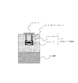
本実施形態に係る光回路素子は、熱光学効果によって導波路の屈折率を変化させ、該導波路に伝搬する光の位相を変化させることによってスイッチングを行うMZI型光スイッチである。図1に示すように、基板10の上には光位相シフト導波路11が設けられており、光位相シフト導波路11の上にはヒーター12が設けられている。光位相シフト導波路11は、SiO2からなるクラッド11aと、Siからなるコア11bとから構成されている。さらに、クラッド11aの内部であって、ヒーター12とコア11bとの間には、伝熱部材としての複数本のカーボンナノチューブ13が配置されている。さらに、各カーボンナノチューブ13は、軸線方向(長手方向)がコア11bの外壁と直交する向きで配置されている。なお、カーボンナノチューブ13の周囲には、クラッド11a(SiO2)ではなく、光吸収が少ない高分子材料を配置してもよい。 The optical circuit element according to the present embodiment is an MZI type optical switch that performs switching by changing the refractive index of a waveguide by a thermo-optic effect and changing the phase of light propagating to the waveguide. As shown in FIG. 1, an optical phase shift waveguide 11 is provided on the substrate 10, and a heater 12 is provided on the optical phase shift waveguide 11. The optical phase shift waveguide 11 includes a clad 11a made of SiO 2 and a core 11b made of Si. Furthermore, a plurality of carbon nanotubes 13 as heat transfer members are disposed inside the clad 11a and between the heater 12 and the core 11b. Furthermore, the carbon nanotubes 13 are arranged such that the axial direction (longitudinal direction) is orthogonal to the outer wall of the core 11b. In addition, a polymer material with little light absorption may be disposed around the carbon nanotubes 13 instead of the cladding 11a (SiO 2 ).
ここで、カーボンナノチューブとは、炭素によって作られた六角網目のシート状構造(グラフェンシート)が単層または多層の同軸管状になった物質である。もっとも、グラフェンシートには、五角網目や七角網目の部分が存在することもある。また、単層のものは「シングルウォールナノチューブ(SWNT)」、複層のものは「マルチウォールナノチューブ(MWNT)」と呼ばれることもある。特に、二層のものは、「ダブルウォールナノチューブ(DWNT)とも呼ばれることもある。本発明におけるカーボンナノチューブには、シングルウォールナノチューブとマルチウォールナノチューブの双方が含まれる。 Here, the carbon nanotube is a substance in which a hexagonal mesh sheet-like structure (graphene sheet) made of carbon is formed into a single-layer or multilayer coaxial tube. However, the graphene sheet may have a pentagonal mesh or a heptagonal mesh. A single-walled one is sometimes called a “single-wall nanotube (SWNT)”, and a multi-layered one is called a “multi-wall nanotube (MWNT)”. In particular, the double-walled one is sometimes referred to as “double wall nanotube (DWNT). The carbon nanotube in the present invention includes both single-wall nanotubes and multi-wall nanotubes.
また、カーボンナノチューブ13の熱伝導率は3000〜5500[W/(m-1K-1)]であり、クラッド11aであるSiO2の熱伝導率は1[W/(m-1K-1)]であり、コア11bであるSiの熱伝導率は168[W/(m-1K-1)]である。これにより、ヒーター12から発せられた熱は、クラッド11aよりも圧倒的に熱伝導率の高いカーボンナノチューブ13を介してコア11bに伝導し、コア11bの全体が効率的に加熱される。さらに、コア11bよりも熱伝導率の低いクラッド11aにより、コア11bの周囲には等価的に熱の分離部が形成される。したがって、ヒーターから発せられた熱が基板10の主面方向に沿ってクラッド11a内を伝導し、基板10に伝導することが少ない。また、クラッド11aの側面や底面から外部に熱が発散することも少ない。すなわち、熱がコア11bに閉じ込められ、コア11bがさらに効率的に加熱される。 The thermal conductivity of the carbon nanotube 13 is 3000 to 5500 [W / (m −1 K −1 )], and the thermal conductivity of SiO 2 as the cladding 11a is 1 [W / (m −1 K −1). ] And the thermal conductivity of Si as the core 11b is 168 [W / (m −1 K −1 )]. As a result, the heat generated from the heater 12 is conducted to the core 11b via the carbon nanotubes 13 that have an overwhelmingly higher thermal conductivity than the clad 11a, and the entire core 11b is efficiently heated. Further, a thermal separation part is equivalently formed around the core 11b by the clad 11a having a lower thermal conductivity than the core 11b. Therefore, the heat generated from the heater is conducted in the clad 11 a along the main surface direction of the substrate 10 and is hardly conducted to the substrate 10. In addition, heat hardly radiates from the side surface or bottom surface of the clad 11a. That is, heat is confined in the core 11b, and the core 11b is heated more efficiently.
さらに、本実施形態では、各カーボンナノチューブ13は、その長手方向がコア11bの外壁と直交する向きで配置されている。換言すれば、カーボンナノチューブ13とコア11bとの接触面積が非常に小さい。よって、カーボンナノチューブ13とコア11bとが直接接触しても、カーボンナノチューブ13による光吸収は非常に少ない。
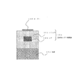
(実施形態2)
以下、本発明の光回路素子の実施形態の他例について図2を参照しながら詳細に説明する。本実施形態に係る光回路素子は、実施形態1に係るMZI型光スイッチと基本構造を共通にするMZI型光スイッチである。
Further, in the present embodiment, the carbon nanotubes 13 are arranged such that the longitudinal direction thereof is orthogonal to the outer wall of the core 11b. In other words, the contact area between the carbon nanotube 13 and the core 11b is very small. Therefore, even if the carbon nanotube 13 and the core 11b are in direct contact, light absorption by the carbon nanotube 13 is very small.
(Embodiment 2)
Hereinafter, another example of the embodiment of the optical circuit element of the present invention will be described in detail with reference to FIG. The optical circuit element according to the present embodiment is an MZI optical switch having the same basic structure as that of the MZI optical switch according to the first embodiment.
本実施形態に係るMZI型光スイッチが実施形態1に係るMZI型光スイッチと異なるのは次の点である。すなわち、本実施形態に係るMZI型光スイッチでは、カーボンナノチューブ13がコア11b中の光モードの存在しない領域のみと接触するように配置されている。これにより、本実施形態に係るMZI型光スイッチでは、カーボンナノチューブ13による光吸収が実施形態1に係るMZI型光スイッチよりも低減される。
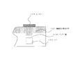
(実施形態3)
以下、本発明の光回路素子の実施形態の他例について図3を参照しながら詳細に説明する。本実施形態に係る光回路素子は、実施形態1に係るMZI型光スイッチと基本構造を共通にするMZI型光スイッチである。
The MZI type optical switch according to the present embodiment is different from the MZI type optical switch according to the first embodiment in the following points. That is, in the MZI type optical switch according to the present embodiment, the carbon nanotubes 13 are arranged so as to contact only the region where the optical mode does not exist in the core 11b. Thereby, in the MZI type optical switch according to the present embodiment, light absorption by the carbon nanotubes 13 is reduced as compared with the MZI type optical switch according to the first embodiment.
(Embodiment 3)
Hereinafter, another example of the embodiment of the optical circuit element of the present invention will be described in detail with reference to FIG. The optical circuit element according to the present embodiment is an MZI optical switch having the same basic structure as that of the MZI optical switch according to the first embodiment.
本実施形態に係るMZI型光スイッチが実施形態1に係るMZI型光スイッチと異なるのは次の点である。すなわち、本実施形態に係るMZI型光スイッチでは、カーボンナノチューブ13は、その長手方向がコア11bの外壁と直交し、かつ、コア11bを伝搬する光の電場の方向と直交する向きで配置されている。なお、本実施形態では、コア11bを伝搬する光の電場の方向は、基板10の主面に対して垂直な方向である。 The MZI type optical switch according to the present embodiment is different from the MZI type optical switch according to the first embodiment in the following points. That is, in the MZI type optical switch according to the present embodiment, the carbon nanotubes 13 are arranged in a direction in which the longitudinal direction is perpendicular to the outer wall of the core 11b and the direction of the electric field of light propagating through the core 11b. Yes. In the present embodiment, the direction of the electric field of light propagating through the core 11 b is a direction perpendicular to the main surface of the substrate 10.
学術論文「Polarization Dependence of the Optical Absorption of Single-Walled Carbon Nanotubes」(PHYSICAL REVIEW LETTERS vol.94(2005) 087402頁)によれば、長手方向と直交する電場を持つ光に対するカーボンナノチューブの光吸収率は、長手方向と平行な電場を持つ光に対する光吸収率の1/100以下である。すなわち、カーボンナノチューブは、光吸収に関して光学異方性を有する。よって、カーボンナノチューブ13が、その長手方向がコア11bの外壁と直交し、かつ、コア11bを伝搬する光の電場と直交する向きで配置されている本実施形態に係るMZI型光スイッチでは、カーボンナノチューブ13による光吸収が実施形態1に係るMZI型光スイッチよりも低減される。 According to the academic paper “Polarization Dependence of the Optical Absorption of Single-Walled Carbon Nanotubes” (PHYSICAL REVIEW LETTERS vol.94 (2005) pp. 087402), The light absorptance for light having an electric field parallel to the longitudinal direction is 1/100 or less. That is, the carbon nanotube has optical anisotropy with respect to light absorption. Therefore, in the MZI optical switch according to this embodiment in which the carbon nanotubes 13 are arranged in a direction in which the longitudinal direction is orthogonal to the outer wall of the core 11b and orthogonal to the electric field of light propagating through the core 11b, Light absorption by the nanotube 13 is reduced as compared with the MZI type optical switch according to the first embodiment.
なお、上記のいずれの実施形態においても、必要十分な伝熱効果が得られる範囲内でカーボンナノチューブの本数を減らすことによって、カーボンナノチューブによる光吸収をより低減することができる。また、上記のいずれの実施形態におけるヒーターも冷却素子に変更することができる。 In any of the above embodiments, the light absorption by the carbon nanotubes can be further reduced by reducing the number of carbon nanotubes within a range in which a necessary and sufficient heat transfer effect can be obtained. The heater in any of the above embodiments can be changed to a cooling element.
本発明は、光通信、光交換、光情報処理および光インターコネクションにおいて、光強度や光位相等の調整に用いられる光可変減衰器や光スイッチに利用することができる。 INDUSTRIAL APPLICABILITY The present invention can be used for an optical variable attenuator and an optical switch that are used for adjusting light intensity, optical phase, and the like in optical communication, optical exchange, optical information processing, and optical interconnection.
10 基板
11 光位相シフト導波路
11a クラッド
11b コア
12 ヒーター
13 カーボンナノチューブ
DESCRIPTION OF SYMBOLS 10 Substrate 11 Optical phase shift waveguide 11a Clad 11b Core 12 Heater 13 Carbon nanotube
Claims (4)
クラッドと、前記クラッドによって覆われたコアとからなる光導波路と、
加熱素子または冷却素子と、
前記クラッド内に埋設され、前記加熱素子または前記冷却素子と前記コアとを熱的に接続する伝熱部材としてのカーボンナノチューブとを有することを特徴とする光回路素子。 An optical circuit element that changes the phase of light propagating through an optical waveguide by a thermo-optic effect,
An optical waveguide comprising a cladding and a core covered by the cladding;
A heating or cooling element;
An optical circuit element comprising carbon nanotubes embedded in the clad and serving as a heat transfer member for thermally connecting the heating element or the cooling element and the core.
Priority Applications (1)
| Application Number | Priority Date | Filing Date | Title |
|---|---|---|---|
| JP2009105272A JP2010256552A (en) | 2009-04-23 | 2009-04-23 | Optical circuit element |
Applications Claiming Priority (1)
| Application Number | Priority Date | Filing Date | Title |
|---|---|---|---|
| JP2009105272A JP2010256552A (en) | 2009-04-23 | 2009-04-23 | Optical circuit element |
Publications (1)
| Publication Number | Publication Date |
|---|---|
| JP2010256552A true JP2010256552A (en) | 2010-11-11 |
Family
ID=43317552
Family Applications (1)
| Application Number | Title | Priority Date | Filing Date |
|---|---|---|---|
| JP2009105272A Pending JP2010256552A (en) | 2009-04-23 | 2009-04-23 | Optical circuit element |
Country Status (1)
| Country | Link |
|---|---|
| JP (1) | JP2010256552A (en) |
Cited By (2)
| Publication number | Priority date | Publication date | Assignee | Title |
|---|---|---|---|---|
| CN104603653A (en) * | 2012-09-13 | 2015-05-06 | 惠普发展公司,有限责任合伙企业 | Controlling temperatures in optical circuits |
| WO2019225445A1 (en) * | 2018-05-21 | 2019-11-28 | 学校法人慶應義塾 | Optical device using nanocarbon material |
-
2009
- 2009-04-23 JP JP2009105272A patent/JP2010256552A/en active Pending
Cited By (4)
| Publication number | Priority date | Publication date | Assignee | Title |
|---|---|---|---|---|
| CN104603653A (en) * | 2012-09-13 | 2015-05-06 | 惠普发展公司,有限责任合伙企业 | Controlling temperatures in optical circuits |
| EP2895898A4 (en) * | 2012-09-13 | 2016-06-08 | Hewlett Packard Development Co | Controlling temperatures in optical circuits |
| US9581761B2 (en) | 2012-09-13 | 2017-02-28 | Hewlett Packard Enterprise Development Lp | Controlling temperatures in optical circuits |
| WO2019225445A1 (en) * | 2018-05-21 | 2019-11-28 | 学校法人慶應義塾 | Optical device using nanocarbon material |
Similar Documents
| Publication | Publication Date | Title |
|---|---|---|
| Yu et al. | Graphene-based transparent flexible heat conductor for thermally tuning nanophotonic integrated devices | |
| Yang et al. | Hyperbolic spoof plasmonic metasurfaces | |
| Yu et al. | Thermally tunable silicon photonic microdisk resonator with transparent graphene nanoheaters | |
| Cheng et al. | Dynamically tunable broadband infrared anomalous refraction based on graphene metasurfaces | |
| Krauss | Why do we need slow light? | |
| Chen et al. | Symmetry-protected transport in a pseudospin-polarized waveguide | |
| Hu et al. | Tunable Fano resonances based on two-beam interference in microring resonator | |
| Liu et al. | Dirac cones at k→= in acoustic crystals and zero refractive index acoustic materials | |
| Hao et al. | Ultra-compact optical modulator by graphene induced electro-refraction effect | |
| Artuso et al. | Optical response of strongly coupled quantum dot− metal nanoparticle systems: double peaked fano structure and bistability | |
| Ye et al. | Electro-absorption optical modulator using dual-graphene-on-graphene configuration | |
| Gong et al. | Photonic crystal cavities in silicon dioxide | |
| Liang et al. | Wideband ultraflat slow light with large group index in a W1 photonic crystal waveguide | |
| Kim et al. | Thermo-optic mode extinction modulator based on graphene plasmonic waveguide | |
| Asgari et al. | Tunable plasmonic dual wavelength multi/demultiplexer based on graphene sheets and cylindrical resonator | |
| Du et al. | The study of few-layer graphene based Mach− Zehnder modulator | |
| Lin et al. | Observation of optical second harmonic generation from suspended single-layer and bi-layer graphene | |
| Liu et al. | Electrically-driven carbon nanotube-based plasmonic laser on silicon | |
| Wang et al. | Tunable broadband transmission and phase modulation of light through graphene multilayers | |
| Yan et al. | Response-time improvement of a 2× 2 thermo-optic switch with polymer/silica hybrid waveguide | |
| JP2010256552A (en) | Optical circuit element | |
| Li et al. | Mach–Zehnder-based five-port silicon router for optical interconnects | |
| Qiu et al. | Guided modes in a two-dimensional metallic photonic crystal waveguide | |
| Francoeur | Nanostructures feel the heat | |
| Wang et al. | Circular dichroism of graphene-based absorber in static magnetic field |