JP2010251663A - Semiconductor device - Google Patents
Semiconductor device Download PDFInfo
- Publication number
- JP2010251663A JP2010251663A JP2009102278A JP2009102278A JP2010251663A JP 2010251663 A JP2010251663 A JP 2010251663A JP 2009102278 A JP2009102278 A JP 2009102278A JP 2009102278 A JP2009102278 A JP 2009102278A JP 2010251663 A JP2010251663 A JP 2010251663A
- Authority
- JP
- Japan
- Prior art keywords
- inductor
- circuit
- semiconductor device
- wiring layer
- substrate
- Prior art date
- Legal status (The legal status is an assumption and is not a legal conclusion. Google has not performed a legal analysis and makes no representation as to the accuracy of the status listed.)
- Granted
Links
Images

Classifications
-
- H—ELECTRICITY
- H10—SEMICONDUCTOR DEVICES; ELECTRIC SOLID-STATE DEVICES NOT OTHERWISE PROVIDED FOR
- H10W—GENERIC PACKAGES, INTERCONNECTIONS, CONNECTORS OR OTHER CONSTRUCTIONAL DETAILS OF DEVICES COVERED BY CLASS H10
- H10W20/00—Interconnections in chips, wafers or substrates
- H10W20/40—Interconnections external to wafers or substrates, e.g. back-end-of-line [BEOL] metallisations or vias connecting to gate electrodes
- H10W20/497—Inductive arrangements or effects of, or between, wiring layers
-
- H—ELECTRICITY
- H10—SEMICONDUCTOR DEVICES; ELECTRIC SOLID-STATE DEVICES NOT OTHERWISE PROVIDED FOR
- H10W—GENERIC PACKAGES, INTERCONNECTIONS, CONNECTORS OR OTHER CONSTRUCTIONAL DETAILS OF DEVICES COVERED BY CLASS H10
- H10W44/00—Electrical arrangements for controlling or matching impedance
- H10W44/501—Inductive arrangements
-
- H—ELECTRICITY
- H10—SEMICONDUCTOR DEVICES; ELECTRIC SOLID-STATE DEVICES NOT OTHERWISE PROVIDED FOR
- H10W—GENERIC PACKAGES, INTERCONNECTIONS, CONNECTORS OR OTHER CONSTRUCTIONAL DETAILS OF DEVICES COVERED BY CLASS H10
- H10W70/00—Package substrates; Interposers; Redistribution layers [RDL]
- H10W70/60—Insulating or insulated package substrates; Interposers; Redistribution layers
- H10W70/611—Insulating or insulated package substrates; Interposers; Redistribution layers for connecting multiple chips together
-
- H—ELECTRICITY
- H10—SEMICONDUCTOR DEVICES; ELECTRIC SOLID-STATE DEVICES NOT OTHERWISE PROVIDED FOR
- H10W—GENERIC PACKAGES, INTERCONNECTIONS, CONNECTORS OR OTHER CONSTRUCTIONAL DETAILS OF DEVICES COVERED BY CLASS H10
- H10W72/00—Interconnections or connectors in packages
-
- H—ELECTRICITY
- H10—SEMICONDUCTOR DEVICES; ELECTRIC SOLID-STATE DEVICES NOT OTHERWISE PROVIDED FOR
- H10W—GENERIC PACKAGES, INTERCONNECTIONS, CONNECTORS OR OTHER CONSTRUCTIONAL DETAILS OF DEVICES COVERED BY CLASS H10
- H10W90/00—Package configurations
-
- H—ELECTRICITY
- H10—SEMICONDUCTOR DEVICES; ELECTRIC SOLID-STATE DEVICES NOT OTHERWISE PROVIDED FOR
- H10W—GENERIC PACKAGES, INTERCONNECTIONS, CONNECTORS OR OTHER CONSTRUCTIONAL DETAILS OF DEVICES COVERED BY CLASS H10
- H10W90/00—Package configurations
- H10W90/20—Configurations of stacked chips
- H10W90/293—Configurations of stacked chips characterised by non-galvanic coupling between the chips, e.g. capacitive coupling
Landscapes
- Semiconductor Integrated Circuits (AREA)
Abstract
【課題】配線基板と送信側の第1回路、及び配線基板と受信側の第2回路とをインダクタ対によって接続するときに、信号を正確に伝達しつつ、第1回路と第2回路の間の絶縁を確保することができるようにする。
【解決手段】配線基板60は、半導体チップ10の第1インダクタ302上から半導体チップ20の第2インダクタ322上に亘って取り付けられている。配線基板60は、第3インダクタ304及び第4インダクタ324を有している。第3インダクタ304は第1インダクタ302の上方に位置している。第1インダクタ302から第3インダクタ304までの距離は、第2インダクタ322から第4インダクタ324までの距離より長い。
【選択図】図1When a wiring board and a first circuit on the transmission side, and a wiring board and a second circuit on the reception side are connected by an inductor pair, the signal is accurately transmitted between the first circuit and the second circuit. So as to ensure insulation.
A wiring board is attached from a first inductor 302 of a semiconductor chip 10 to a second inductor 322 of a semiconductor chip 20. The wiring board 60 has a third inductor 304 and a fourth inductor 324. The third inductor 304 is located above the first inductor 302. The distance from the first inductor 302 to the third inductor 304 is longer than the distance from the second inductor 322 to the fourth inductor 324.
[Selection] Figure 1
Description
本発明は、入力される電気信号の電位が互いに異なる2つの回路の間で電気信号を伝達することができる半導体装置に関する。 The present invention relates to a semiconductor device capable of transmitting an electric signal between two circuits having different electric signal potentials.
入力される電気信号の電位が互いに異なる2つの回路の間で電気信号を伝達する場合、フォトカプラを用いることが多い。フォトカプラは、発光ダイオードなどの発光素子とフォトトランジスタなどの受光素子を有しており、入力された電気信号を発光素子で光に変換し、この光を受光素子で電気信号に戻すことにより、電気信号を伝達している。 When an electric signal is transmitted between two circuits having different electric signal potentials, a photocoupler is often used. The photocoupler has a light emitting element such as a light emitting diode and a light receiving element such as a phototransistor. An electrical signal is transmitted.
しかし、フォトカプラは発光素子と受光素子を有しているため、小型化が難しい。また、電気信号の周波数が高い場合には電気信号に追従できなくなる。これらの問題を解決する技術として、例えば特許文献1に記載されているように、2つのインダクタを誘導結合させることにより、電気信号を伝達する技術が開発されている。 However, since the photocoupler has a light emitting element and a light receiving element, it is difficult to reduce the size. Further, when the frequency of the electrical signal is high, it becomes impossible to follow the electrical signal. As a technique for solving these problems, a technique for transmitting an electric signal by inductively coupling two inductors has been developed as described in, for example, Patent Document 1.
また特許文献2には、送信側の第1半導体チップと受信側の第2半導体チップとを伝送経路を介して相互に接続する際に、インダクタ対を用いることが記載されている。詳細には、伝送線路と第1半導体チップは、送信側インダクタ対の電磁結合によって非接触に接続している。また伝送線路と第2半導体チップは、受信側インダクタ対の電磁結合によって非接触に接続している。 Patent Document 2 describes that an inductor pair is used when a first semiconductor chip on a transmission side and a second semiconductor chip on a reception side are connected to each other via a transmission path. Specifically, the transmission line and the first semiconductor chip are connected in a non-contact manner by electromagnetic coupling of the transmission-side inductor pair. The transmission line and the second semiconductor chip are connected in a non-contact manner by electromagnetic coupling of the receiving-side inductor pair.
送信側の回路と受信側の回路とを配線基板を介して接続する場合において、送信側の回路と配線基板とをインダクタ対で接続し、配線基板と受信側の回路とをインダクタ対によって接続することが考えられる。この場合、インダクタ対が2つになるため、信号が伝達する間に減衰し、信号が正確に伝達できない可能性がでてくる。信号を正確に伝達するためには、インダクタ対を構成する2つのインダクタの相互間隔を狭くすれば良い。しかし、送信側の回路と受信側の回路の基準電圧が異なる場合、2つのインダクタ対それぞれにおいて、インダクタ対を構成する2つのインダクタの相互間隔を狭くすると、送信側の回路と受信側の回路の間の絶縁を確保できなくなる。このように、信号を正確に伝達しつつ、送信側の回路と受信側の回路の間の絶縁を確保することは難しかった。 When connecting the circuit on the transmission side and the circuit on the reception side via a wiring board, the circuit on the transmission side and the wiring board are connected by an inductor pair, and the circuit board and the circuit on the reception side are connected by an inductor pair. It is possible. In this case, since there are two inductor pairs, the signal is attenuated during transmission, and the signal may not be transmitted accurately. In order to transmit a signal accurately, the distance between the two inductors constituting the inductor pair may be narrowed. However, if the reference voltages of the transmission side circuit and the reception side circuit are different, if the mutual distance between the two inductors constituting the inductor pair is reduced in each of the two inductor pairs, the transmission side circuit and the reception side circuit Insulation between them cannot be secured. As described above, it is difficult to ensure insulation between the transmission side circuit and the reception side circuit while accurately transmitting the signal.
本発明によれば、配線層を有する一つまたは二つの半導体チップ、及び前記一つまたは二つの半導体チップの配線層側に取り付けられた配線基板を備え、
前記一つまたは二つの半導体チップは、
信号を生成する第1回路と、
前記配線層に形成され、前記第1回路に接続された第1インダクタと、
前記信号を処理する第2回路と、
前記配線層に形成され、前記第2回路に接続された第2インダクタと、
を有し、
前記配線基板は、
前記第1インダクタの上方に位置する第3インダクタと、
前記第2インダクタの上方に位置し、前記第3インダクタに接続している第4インダクタと、
を有し、
前記第1インダクタから前記第3インダクタまでの距離は、前記第2インダクタから前記第4インダクタまでの距離と異なる半導体装置が提供される。
According to the present invention, comprising one or two semiconductor chips having a wiring layer, and a wiring board attached to the wiring layer side of the one or two semiconductor chips,
The one or two semiconductor chips are:
A first circuit for generating a signal;
A first inductor formed in the wiring layer and connected to the first circuit;
A second circuit for processing the signal;
A second inductor formed in the wiring layer and connected to the second circuit;
Have
The wiring board is
A third inductor located above the first inductor;
A fourth inductor located above the second inductor and connected to the third inductor;
Have
A semiconductor device is provided in which a distance from the first inductor to the third inductor is different from a distance from the second inductor to the fourth inductor.
本発明によれば、第1インダクタから第3インダクタまでの距離は、第2インダクタから第4インダクタまでの距離と異なっている。第1回路と第2回路の間の耐圧は、第1インダクタから第3インダクタまでの距離と、第2インダクタから第4インダクタまでの距離の和によって定まる。このため、第1インダクタから第3インダクタまでの距離と、第2インダクタから第4インダクタまでの距離の和は、ある値以上を有する必要がある。半導体装置を設計する場合、上記した必要な値を、第1インダクタから第3インダクタまでの距離と、第2インダクタから第4インダクタまでの距離に配分することになる。第1インダクタから第3インダクタまでの距離、及び第2インダクタと第4インダクタの距離をそれぞれ互いに異ならせ、適切な値にすれば、第1回路から第2回路までの信号伝達効率を最大値にすることができる。従って、信号を正確に伝達しつつ、第1回路と第2回路の間の絶縁を確保することができる。 According to the present invention, the distance from the first inductor to the third inductor is different from the distance from the second inductor to the fourth inductor. The withstand voltage between the first circuit and the second circuit is determined by the sum of the distance from the first inductor to the third inductor and the distance from the second inductor to the fourth inductor. For this reason, the sum of the distance from the first inductor to the third inductor and the distance from the second inductor to the fourth inductor needs to have a certain value or more. When designing a semiconductor device, the necessary values described above are distributed to the distance from the first inductor to the third inductor and the distance from the second inductor to the fourth inductor. If the distance from the first inductor to the third inductor and the distance between the second inductor and the fourth inductor are different from each other and set to appropriate values, the signal transmission efficiency from the first circuit to the second circuit is maximized. can do. Therefore, it is possible to ensure insulation between the first circuit and the second circuit while accurately transmitting the signal.
本発明によれば、配線基板と送信側の第1回路、及び配線基板と受信側の第2回路とをインダクタ対によって接続するときに、信号を正確に伝達しつつ、第1回路と第2回路の間の絶縁を確保することができる。 According to the present invention, when the wiring board and the first circuit on the transmission side, and the wiring board and the second circuit on the reception side are connected by the inductor pair, the first circuit and the second circuit are transmitted while accurately transmitting the signal. Insulation between the circuits can be ensured.
以下、本発明の実施の形態について、図面を用いて説明する。尚、すべての図面において、同様な構成要素には同様の符号を付し、適宜説明を省略する。 Hereinafter, embodiments of the present invention will be described with reference to the drawings. In all the drawings, the same reference numerals are given to the same components, and the description will be omitted as appropriate.
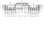
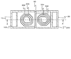
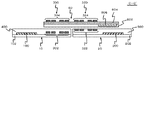
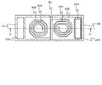
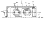
図1は、第1の実施形態に係る半導体装置の構成を示す図であり、図2は図1に示した半導体装置の平面概略図である。図1は図2のA−A´断面に相当している。なお図1において、図を簡略化するため、後述する第1インダクタ302及び第2インダクタ322の巻き数を図2と異ならせている。この半導体装置は、二つの半導体チップ10,20及び配線基板60を備える。半導体チップ10は多層配線層400を有しており、半導体チップ20は多層配線層500を有している。
FIG. 1 is a diagram showing a configuration of the semiconductor device according to the first embodiment, and FIG. 2 is a schematic plan view of the semiconductor device shown in FIG. FIG. 1 corresponds to the AA ′ cross section of FIG. In FIG. 1, in order to simplify the drawing, the number of turns of a
半導体チップ10は、第1基板102、第1回路100、及び第1インダクタ302を有している。第1基板102はシリコン基板などの半導体基板である。第1回路100は送信される信号を生成する。第1インダクタ302は多層配線層400に形成されている。第1インダクタ302は、第1回路100に接続しており、第1回路100で生成した信号が入力される。
The
半導体チップ20は、第2基板202、第2回路200及び第2インダクタ322を有している。第2基板202はシリコン基板などの半導体基板である。第2回路200は、第1回路100が生成した信号を受信して処理する。第2インダクタ322は多層配線層500に形成されている。第2インダクタ322は、第2回路200に接続しており、第2回路200に信号を伝達する。伝達される信号は、例えばデジタル信号であるが、アナログ信号であっても良い。
The
配線基板60は、半導体チップ10の第1インダクタ302上から半導体チップ20の第2インダクタ322上に亘って取り付けられている。配線基板60は、例えば接着剤(図示せず)を介して、半導体チップ10及び半導体チップ20に取り付けられている。配線基板60は、第3インダクタ304及び第4インダクタ324を有している。第3インダクタ304は第1インダクタ302の上方に位置している。第4インダクタ324は、第2インダクタ322の上方に位置しており、第3インダクタ304に接続している。第1インダクタ302から第3インダクタ304までの距離は、第2インダクタ322から第4インダクタ324までの距離より長い。各インダクタは、渦巻き型の配線パターンである。
The
図1に示す例において、配線基板60は、シリコン基板602を用いて形成されたシリコンインターポーザである。ただし、配線基板60は、樹脂製の基板を用いたインターポーザや配線基板であってもよい。また配線基板60がシリコン基板602を用いて形成されており、第1基板102及び第2基板202がシリコン基板である場合、配線基板60のシリコン基板の不純物濃度は、第1基板102の基板不純物濃度及び第2基板202の基板不純物濃度より低いのが好ましい。このようにすると、シリコン基板602に渦電流が発生することを抑制できる。
In the example shown in FIG. 1, the
本実施形態では、第3インダクタ304及び第4インダクタ324は、配線基板60のうち半導体チップ10及び半導体チップ20とは反対側の面に形成されている。なお第3インダクタ304及び第4インダクタ324は、シリコン基板602上に形成された配線層604に形成されている。配線層604は多層配線層であり、第3インダクタ304及び第4インダクタ324は、配線層604内の配線(図示せず)を介して互いに接続している。
In the present embodiment, the
第1インダクタ302及び第3インダクタ304は、第1信号伝達素子300を構成しており、第2インダクタ322及び第4インダクタ324は第2信号伝達素子320を構成している。上記したように、第1インダクタ302から第3インダクタ304までの距離は、第2インダクタ322から第4インダクタ324までの距離と異なっている。
The
詳細には、第1インダクタ302は半導体チップ10の多層配線層400に形成されており、第2インダクタ322は半導体チップ20の多層配線層500に形成されている。多層配線層400,500は、絶縁層及び配線層をこの順にそれぞれ複数回以上交互に積層したものである。本実施形態において、多層配線層400は、絶縁層410、配線層412、絶縁層420、配線層422、絶縁層430、配線層432、絶縁層440、及び配線層442をこの順に重ねた構成を有している。また多層配線層500は、絶縁層510、配線層512、絶縁層520、配線層522、絶縁層530、配線層532、絶縁層540、及び配線層542をこの順に重ねた構成を有している。各絶縁層は、複数の絶縁膜を積層した構造であってもよいし、一つの絶縁膜であってもよい。なお、多層配線層400,500は、保護膜(図示せず)により被覆されている。また多層配線層400,500の層数は互いに同じであっても良いし、異なっていても良い。
Specifically, the
本図に示す例において、第1インダクタ302は、多層配線層400の第1配線層である配線層412に設けられており、第2インダクタ322は、多層配線層500の最上層の配線層542に設けられている。
In the example shown in this figure, the
各配線層の配線は、ダマシン法により形成されたCu配線であり、それぞれ配線層に形成された溝に埋め込まれている。最上層の配線には、パッド(図示せず)が形成されている。なお、多層配線層400,500において、配線層の少なくとも一つはAl合金配線であっても良い。なお各配線層に形成された配線は、絶縁層に埋め込まれたプラグを介して互いに接続している。 The wiring in each wiring layer is a Cu wiring formed by a damascene method, and is embedded in a groove formed in each wiring layer. A pad (not shown) is formed on the uppermost wiring layer. In the multilayer wiring layers 400 and 500, at least one of the wiring layers may be an Al alloy wiring. Note that the wirings formed in each wiring layer are connected to each other through plugs embedded in the insulating layer.
絶縁層及び配線層を構成する各絶縁膜はSiO2膜であっても良いし、低誘電率膜であってもよい。低誘電率膜は、例えば比誘電率が3.3以下、好ましくは2.9以下の絶縁膜とすることができる。低誘電率膜としては、SiOCの他に、HSQ(ハイドロジェンシルセスキオキサン)、MSQ(メチルシルセスキオキサン)、またはMHSQ(メチル化ハイドロジェンシルセスキオキサン)等のポリハイドロジェンシロキサン、ポリアリールエーテル(PAE)、ジビニルシロキサン‐ビス‐ベンゾシクロブテン(BCB)、またはSilk(登録商標)等の芳香族含有有機材料、SOG、FOX(flowable oxide)(登録商標)、サイトップ(登録商標)、またはBCB(Bensocyclobutene)等を用いることもできる。また、低誘電率膜としては、これらの多孔質膜を用いることもできる。 Each insulating film constituting the insulating layer and the wiring layer may be a SiO 2 film or a low dielectric constant film. The low dielectric constant film can be an insulating film having a relative dielectric constant of 3.3 or less, preferably 2.9 or less, for example. As the low dielectric constant film, in addition to SiOC, polyhydrogensiloxane such as HSQ (hydrogen silsesquioxane), MSQ (methyl silsesquioxane), or MHSQ (methylated hydrogen silsesquioxane), Aromatic-containing organic materials such as polyaryl ether (PAE), divinylsiloxane-bis-benzocyclobutene (BCB), or Silk (registered trademark), SOG, FOX (flowable oxide) (registered trademark), Cytop (registered trademark) ) Or BCB (Bencyclocyclene) or the like can also be used. Moreover, these porous films can also be used as the low dielectric constant film.
なお、多層配線層400と多層配線層500の厚さが異なる場合、配線基板60が傾くことが考えられる。この場合、第1基板102と第2基板202の裏面研削量を変えて半導体チップ10及び半導体チップ20の厚さを同じにすればよい。
In addition, when the thickness of the
第1回路100は送信回路であり、第2回路200は受信回路である。このため、第1インダクタ302は送信側インダクタとして機能し、第3インダクタ304は受信側インダクタとして機能する。また第4インダクタ324は送信側インダクタとして機能し、第2インダクタ322は受信側インダクタとして機能する。
The
第1回路100は、例えば送信側ドライバ回路(例えばゲートドライバ)であり、デジタル信号を変調した送信用の信号を増幅して第1インダクタ302に出力する。第2回路200は、例えば受信側ドライバ回路(例えばゲートドライバ)であり、第2インダクタ322が受信した信号を変調することにより生成したデジタル信号を増幅して出力する。
The
第1回路100及び第2回路200は、入力される電気信号の電位が互いに異なるが、第1信号伝達素子300及び第2信号伝達素子320は誘導結合を用いて電気信号を伝達するため、第1回路100及び第2回路200に問題は生じない。なお図1の構成において、「入力される電気信号の電位が互いに異なる」場合として、電気信号の振幅(0を示す電位と1を示す電位の差)が互いに異なる場合、電気信号の基準電位(0を示す電位)が異なる場合、及び電気信号の振幅が互いに異なり、かつ電気信号の基準電位が異なる場合などがある。
Although the
半導体チップ10の第1回路100は第1トランジスタを有している。第1トランジスタには、N型のトランジスタとP型のトランジスタがある。N型の第1トランジスタ121はP型のウェル120に形成されており、ソース及びドレインとなる2つのN型の不純物領域124及びゲート電極126を有している。P型の第1トランジスタ141はN型のウェル140に形成されており、ソース及びドレインとなる2つのP型の不純物領域144及びゲート電極146を有している。ゲート電極126,146それぞれの下にはゲート絶縁膜が位置している。これら2つのゲート絶縁膜は、厚さが略等しい。そして第1トランジスタ121,141は、上記した送信側ドライバ回路、例えばインバータを構成している。
The
ウェル120にはP型の不純物領域122が形成されており、ウェル140にはN型の不純物領域142が形成されている。不純物領域122にはN型の第1トランジスタ121の基準電位(グラウンド電位)を与える配線が接続されており、不純物領域142にはP型の第1トランジスタ141の電源電位を与える配線が接続されている。
A P-
半導体チップ20の第2回路200は第2トランジスタを有している。第2トランジスタにも、N型のトランジスタと、P型のトランジスタがある。N型の第2トランジスタ221はP型のウェル220に形成されており、ソース及びドレインとなる2つのN型の不純物領域224及びゲート電極226を有している。P型の第2トランジスタ241はN型のウェル240に形成されており、ソース及びドレインとなる2つのP型の不純物領域244及びゲート電極246を有している。ゲート電極226,246それぞれの下にはゲート絶縁膜が位置している。そして第2トランジスタ221,241は、上記した受信側ドライバ回路、例えばインバータを構成している。
The
ウェル220にはP型の不純物領域222が形成されており、ウェル240にはN型の不純物領域242が形成されている。不純物領域222にはN型の第2トランジスタ221の基準電位を与える配線が接続されており、不純物領域242にはP型の第2トランジスタ241の電源電位を与える配線が接続されている。 A P-type impurity region 222 is formed in the well 220, and an N-type impurity region 242 is formed in the well 240. A wiring for supplying a reference potential of the N-type second transistor 221 is connected to the impurity region 222, and a wiring for supplying a power supply potential of the P-type second transistor 241 is connected to the impurity region 242.
本図に示す例において、第1トランジスタ121,141と第2トランジスタ221,241は、ゲート絶縁膜の厚さが互いに異なっているが、同じであっても良い。
In the example shown in the figure, the
なお、配線基板60の面積は、半導体チップ10の面積と半導体チップ20の面積の和より小さい。
The area of the
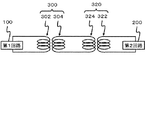
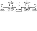
図3は、図1に示した半導体装置の等価回路図である。第1回路100で生成した信号は、第1信号伝達素子300及び第2信号伝達素子320を介して、第2回路200に受信される。第1信号伝達素子300は、第1インダクタ302と第3インダクタ304の誘導結合によって信号を伝達し、第2信号伝達素子320は、第4インダクタ324と第2インダクタ322の誘導結合によって信号を伝達する。
FIG. 3 is an equivalent circuit diagram of the semiconductor device shown in FIG. The signal generated by the
次に、本実施形態の作用及び効果について説明する。第1回路100と第2回路200は、入力される電気信号の電位が互いに異なる。第1回路100と第2回路200の間の耐圧は、第1インダクタ302と第3インダクタ304の間隔と、第2インダクタ322と第4インダクタ324の間隔の和によって定まる。このため、第1インダクタ302と第3インダクタ304の間隔と、第2インダクタ322と第4インダクタ324の間隔の和は、ある値以上になる必要がある。そして、半導体装置を設計する場合、上記した必要な値を、第1インダクタ302と第3インダクタ304の間隔と、第2インダクタ322と第4インダクタ324の間隔に配分することになる。第1インダクタ302と第3インダクタ304の間隔、及び第2インダクタ322と第4インダクタ324までの間隔をそれぞれ互いに異ならせ、適切な値にすれば、第1回路100から第2回路200までの信号伝達効率を最大値にすることができる。本実施形態では、第1インダクタ302から第3インダクタ304までの距離は、第2インダクタ322から第4インダクタ324までの距離と異なっている。従って、信号を正確に伝達しつつ、第1回路100と第2回路200の間の絶縁を確保することができる。
Next, the operation and effect of this embodiment will be described. The
例えば、第1信号伝達素子300の送信側インダクタである第1インダクタ302は、送信回路である第1回路100に接続しているため、比較的大きな電流が流れる。これに対して第2信号伝達素子320の送信側インダクタである第4インダクタ324は、第1信号伝達素子300の受信側インダクタである第3インダクタ304に流れた誘導電流が流れるため、比較的小さな電流が流れる。このため、第1信号伝達素子300の受信側インダクタである第3インダクタ304には、相対的に大きな誘導電流が生じ、第2信号伝達素子320の受信側インダクタである第2インダクタ322には、相対的に小さな誘導電流が生じる。そこで本実施形態のように、第1インダクタ302を多層配線層400の最下層の配線層412に配置して、第2インダクタ322を多層配線層500の最上層の配線層に配置すると、第1信号伝達素子300内で耐圧を確保しつつ、第2信号伝達素子320の信号伝達効率を高くすることができる。
For example, since the
また本実施形態では、第3インダクタ304は、配線基板60のうち半導体チップ10とは反対側の面に形成されている。このため、第1インダクタ302と第3インダクタ304を離して、第1信号伝達素子300の耐圧を大きくすることができる。
In the present embodiment, the
また、配線基板60のシリコン基板602の基板不純物濃度を、第1基板102の基板不純物濃度及び第2基板202の基板不純物濃度より低くすると、第1信号伝達素子300及び第2信号伝達素子320が生じる磁場によって、シリコン基板602に渦電流が生じることが抑制される。
Further, when the substrate impurity concentration of the silicon substrate 602 of the
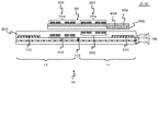
図4は、第2の実施形態に係る半導体装置の構成を示す断面図であり、図5は図4に示した半導体装置の平面概略図である。図4は図5のB−B´断面に相当している。この半導体装置は、第3インダクタ304及び第4インダクタ324が、配線基板60のうち半導体チップ10及び半導体チップ20に対向する面に形成されている点を除いて、第1の実施形態に係る半導体装置と同様の構成である。
FIG. 4 is a cross-sectional view showing the configuration of the semiconductor device according to the second embodiment, and FIG. 5 is a schematic plan view of the semiconductor device shown in FIG. 4 corresponds to the BB ′ cross section of FIG. This semiconductor device is the same as the semiconductor device according to the first embodiment except that the
本実施形態によっても、信号を正確に伝達しつつ、第1回路100と第2回路200の間の絶縁を確保することができる。また、第4インダクタ324は、配線基板60のうち半導体チップ20に対向する面に形成されている。このため、第4インダクタ324と第2インダクタ322を近づけて、第2信号伝達素子320の信号伝達効率を大きくすることができる。
Also according to the present embodiment, it is possible to ensure insulation between the
図6は、第3の実施形態に係る半導体装置の構成を示す断面概略図であり、図7は、図6に示した半導体装置の平面概略図である。図6は図7のC−C´断面に相当している。この半導体装置は、シリコン基板602のうち配線層604が形成されている面に送受信回路606が形成されている点を除いて、第1の実施形態と同様の構成である。
FIG. 6 is a schematic cross-sectional view showing the configuration of the semiconductor device according to the third embodiment, and FIG. 7 is a schematic plan view of the semiconductor device shown in FIG. FIG. 6 corresponds to the CC ′ cross section of FIG. This semiconductor device has the same configuration as that of the first embodiment except that the transmission /
図8は、図6及び図7に示した半導体装置の等価回路図である。送受信回路606は、回路上において第3インダクタ304と第4インダクタ324の間に設けられている。送受信回路606は、受信回路及び送信回路を有しており、第3インダクタ304が第1インダクタ302から受信した信号を復調した後、再度変調して第4インダクタ324に出力する。図6に示すように送受信回路606は、配線基板60のうち配線層604が形成された面に形成されているが、配線層604が形成された面とは逆の面に形成されても良い。
FIG. 8 is an equivalent circuit diagram of the semiconductor device shown in FIGS. The transmission /
本実施形態によっても、第1又は第2の実施形態と同様の効果を得ることができる。また、送受信回路606は、第3インダクタ304が第1インダクタ302から受信した信号を復調した後、再度変調して第4インダクタ324に出力する。このため、信号伝達効率がさらに向上する。
According to this embodiment, the same effect as that of the first or second embodiment can be obtained. In addition, the transmission /
図9は、第4の実施形態に係る半導体装置の構成を示す断面概略図であり、図10は図9に示した半導体装置の平面概略図である。図9は図10のD−D´断面に相当している。この半導体装置は、第1回路100及び第1インダクタ302は半導体チップ10の第1領域12に形成されており、第2回路200及び第2インダクタ322は半導体チップ10の第2領域14に形成されている点を除いて、第1〜第3の実施形態のいずれかと同様の構成である。なお図9及び図10は、第3の実施形態と同様の場合を示している。
FIG. 9 is a schematic cross-sectional view showing the configuration of the semiconductor device according to the fourth embodiment, and FIG. 10 is a schematic plan view of the semiconductor device shown in FIG. FIG. 9 corresponds to the section DD ′ in FIG. In this semiconductor device, the
第1基板102はSOI(Silicon On Insulator)基板であり、シリコン基板104上に絶縁層106及びシリコン層108をこの順に積層した構成である。シリコン層108には、第1領域12及び第2領域14を絶縁する絶縁分離層109が埋め込まれている。絶縁分離層109の下端は、絶縁層106に達している。
The
本実施形態によっても、第1〜第3の実施形態と同様の効果を得ることができる。また半導体チップ10に、送信回路としての第1回路100及び受信回路としての第2回路200を形成することができる。
Also according to the present embodiment, the same effects as those of the first to third embodiments can be obtained. In addition, a
以上、図面を参照して本発明の実施形態について述べたが、これらは本発明の例示であり、上記以外の様々な構成を採用することもできる。 As mentioned above, although embodiment of this invention was described with reference to drawings, these are the illustrations of this invention, Various structures other than the above are also employable.
10 半導体チップ
12 第1領域
14 第2領域
20 半導体チップ
60 配線基板
100 第1回路
102 第1基板
104 シリコン基板
106 絶縁層
108 シリコン層
109 絶縁分離層
120 ウェル
121 第1トランジスタ
122 不純物領域
124 不純物領域
126 ゲート電極
140 ウェル
141 第1トランジスタ
142 不純物領域
144 不純物領域
146 ゲート電極
200 第2回路
202 第2基板
220 ウェル
221 第2トランジスタ
222 不純物領域
224 不純物領域
226 ゲート電極
240 ウェル
241 第2トランジスタ
242 不純物領域
244 不純物領域
246 ゲート電極
300 第1信号伝達素子
302 第1インダクタ
304 第3インダクタ
320 第2信号伝達素子
322 第2インダクタ
324 第4インダクタ
400 多層配線層
410 絶縁層
412 配線層
420 絶縁層
422 配線層
430 絶縁層
432 配線層
440 絶縁層
442 配線層
500 多層配線層
510 絶縁層
512 配線層
520 絶縁層
522 配線層
530 絶縁層
532 配線層
540 絶縁層
542 配線層
602 シリコン基板
604 配線層
606 送受信回路
10
Claims (8)
前記一つまたは二つの半導体チップは、
信号を生成する第1回路と、
前記配線層に形成され、前記第1回路に接続された第1インダクタと、
前記信号を処理する第2回路と、
前記配線層に形成され、前記第2回路に接続された第2インダクタと、
を有し、
前記配線基板は、
前記第1インダクタの上方に位置する第3インダクタと、
前記第2インダクタの上方に位置し、前記第3インダクタに接続している第4インダクタと、
を有し、
前記第1インダクタから前記第3インダクタまでの距離は、前記第2インダクタから前記第4インダクタまでの距離と異なる半導体装置。 One or two semiconductor chips having a wiring layer, and a wiring board attached to the wiring layer side of the one or two semiconductor chips,
The one or two semiconductor chips are:
A first circuit for generating a signal;
A first inductor formed in the wiring layer and connected to the first circuit;
A second circuit for processing the signal;
A second inductor formed in the wiring layer and connected to the second circuit;
Have
The wiring board is
A third inductor located above the first inductor;
A fourth inductor located above the second inductor and connected to the third inductor;
Have
A semiconductor device in which a distance from the first inductor to the third inductor is different from a distance from the second inductor to the fourth inductor.
前記第1インダクタから前記第3インダクタまでの距離は、前記第2インダクタから前記第4インダクタまでの距離より長い半導体装置。 The semiconductor device according to claim 1,
A semiconductor device in which a distance from the first inductor to the third inductor is longer than a distance from the second inductor to the fourth inductor.
前記配線基板はシリコン基板を用いて形成されている半導体装置。 The semiconductor device according to claim 1 or 2,
A semiconductor device in which the wiring substrate is formed using a silicon substrate.
前記一つまたは二つの半導体チップはシリコン基板を用いて形成されており、
前記配線基板における基板不純物濃度は、前記一つまたは二つの半導体チップの基板不純物濃度より低い半導体装置。 The semiconductor device according to claim 3.
The one or two semiconductor chips are formed using a silicon substrate,
A semiconductor device wherein a substrate impurity concentration in the wiring substrate is lower than a substrate impurity concentration of the one or two semiconductor chips.
前記配線基板に形成され、回路上において前記第3インダクタと前記第4インダクタの間に設けられた送受信回路を備える半導体装置。 The semiconductor device according to claim 3 or 4,
A semiconductor device comprising: a transmission / reception circuit formed on the wiring board and provided between the third inductor and the fourth inductor on the circuit.
前記第3インダクタ及び前記第4インダクタは、前記配線基板のうち前記一つまたは二つの半導体チップとは反対側の面に形成されている半導体装置。 In the semiconductor device according to any one of claims 1 to 5,
The third inductor and the fourth inductor are semiconductor devices formed on a surface of the wiring board opposite to the one or two semiconductor chips.
前記第1回路及び前記第1インダクタは第1の前記半導体チップに形成されており、
前記第2回路及び前記第2インダクタは第2の前記半導体チップに形成されており、
前記配線基板は、前記第1の半導体チップ上から前記第2の半導体チップ上に亘って取り付けられている半導体装置。 In the semiconductor device according to claim 1,
The first circuit and the first inductor are formed in the first semiconductor chip;
The second circuit and the second inductor are formed in the second semiconductor chip,
The semiconductor device, wherein the wiring board is attached from the first semiconductor chip to the second semiconductor chip.
前記第1回路、前記第2回路、前記第1インダクタ、及び前記第2インダクタは一つの前記半導体チップに形成されており、
前記第1回路及び前記第1インダクタは前記半導体チップの第1領域に形成されており、
前記第2回路及び前記第2インダクタは前記半導体チップの第2領域に形成されており、
前記第1領域及び前記第2領域は絶縁されている半導体装置。 In the semiconductor device according to claim 1,
The first circuit, the second circuit, the first inductor, and the second inductor are formed on one semiconductor chip;
The first circuit and the first inductor are formed in a first region of the semiconductor chip;
The second circuit and the second inductor are formed in a second region of the semiconductor chip;
A semiconductor device in which the first region and the second region are insulated.
Priority Applications (4)
| Application Number | Priority Date | Filing Date | Title |
|---|---|---|---|
| JP2009102278A JP5496541B2 (en) | 2009-04-20 | 2009-04-20 | Semiconductor device |
| US12/662,442 US8310025B2 (en) | 2009-04-20 | 2010-04-16 | Semiconductor device |
| US13/667,955 US8810042B2 (en) | 2009-04-20 | 2012-11-02 | Semiconductor device |
| US14/328,458 US9496220B2 (en) | 2009-04-20 | 2014-07-10 | Semiconductor device |
Applications Claiming Priority (1)
| Application Number | Priority Date | Filing Date | Title |
|---|---|---|---|
| JP2009102278A JP5496541B2 (en) | 2009-04-20 | 2009-04-20 | Semiconductor device |
Related Child Applications (1)
| Application Number | Title | Priority Date | Filing Date |
|---|---|---|---|
| JP2014042515A Division JP5749366B2 (en) | 2014-03-05 | 2014-03-05 | Semiconductor device |
Publications (3)
| Publication Number | Publication Date |
|---|---|
| JP2010251663A true JP2010251663A (en) | 2010-11-04 |
| JP2010251663A5 JP2010251663A5 (en) | 2012-06-07 |
| JP5496541B2 JP5496541B2 (en) | 2014-05-21 |
Family
ID=42980368
Family Applications (1)
| Application Number | Title | Priority Date | Filing Date |
|---|---|---|---|
| JP2009102278A Expired - Fee Related JP5496541B2 (en) | 2009-04-20 | 2009-04-20 | Semiconductor device |
Country Status (2)
| Country | Link |
|---|---|
| US (3) | US8310025B2 (en) |
| JP (1) | JP5496541B2 (en) |
Cited By (5)
| Publication number | Priority date | Publication date | Assignee | Title |
|---|---|---|---|---|
| WO2016157387A1 (en) * | 2015-03-30 | 2016-10-06 | 株式会社PEZY Computing | Semiconductor device |
| US10269734B2 (en) | 2015-07-16 | 2019-04-23 | Ultramemory Inc. | Semiconductor element |
| JP2019153685A (en) * | 2018-03-02 | 2019-09-12 | ルネサスエレクトロニクス株式会社 | Semiconductor device |
| JP2023046880A (en) * | 2021-09-24 | 2023-04-05 | 株式会社東芝 | semiconductor equipment |
| JP2024039782A (en) * | 2022-09-12 | 2024-03-25 | 株式会社東芝 | isolator |
Families Citing this family (12)
| Publication number | Priority date | Publication date | Assignee | Title |
|---|---|---|---|---|
| JP5578797B2 (en) | 2009-03-13 | 2014-08-27 | ルネサスエレクトロニクス株式会社 | Semiconductor device |
| IT1404038B1 (en) | 2010-12-29 | 2013-11-08 | St Microelectronics Srl | ELECTRONIC SEMICONDUCTOR DEVICE PROVIDED WITH AN INTEGRATED GALVANIC INSULATOR ELEMENT, AND RELATIVE ASSEMBLY PROCEDURE |
| US9337905B2 (en) | 2013-07-01 | 2016-05-10 | Texas Instruments Incorporated | Inductive structures with reduced emissions and interference |
| US20150077208A1 (en) * | 2013-09-16 | 2015-03-19 | Ken Goldman | High-q parallel-trace planar spiral coil for biomedical implants |
| JP6395304B2 (en) * | 2013-11-13 | 2018-09-26 | ローム株式会社 | Semiconductor device and semiconductor module |
| CN105659340B (en) * | 2014-01-15 | 2019-03-22 | 株式会社村田制作所 | circuit |
| US9997495B2 (en) * | 2014-12-19 | 2018-06-12 | Elwha Llc | Non-contacting inductive interconnects |
| CN209590845U (en) * | 2016-12-02 | 2019-11-05 | 株式会社村田制作所 | Auxiliary antenna, RFID system |
| US10438906B2 (en) * | 2016-12-07 | 2019-10-08 | Nxp Usa, Inc. | Radio frequency (RF) inductive signal coupler and method therefor |
| JP7437275B2 (en) | 2020-09-09 | 2024-02-22 | 株式会社東芝 | electronic device |
| JP7686394B2 (en) * | 2020-12-24 | 2025-06-02 | ローム株式会社 | Gate Driver |
| JP7638183B2 (en) * | 2021-09-02 | 2025-03-03 | ルネサスエレクトロニクス株式会社 | Semiconductor Device |
Citations (4)
| Publication number | Priority date | Publication date | Assignee | Title |
|---|---|---|---|---|
| JP2006246372A (en) * | 2005-03-07 | 2006-09-14 | Fuji Xerox Co Ltd | Relay antenna for rfid and rfid system |
| JP2007235034A (en) * | 2006-03-03 | 2007-09-13 | Seiko Epson Corp | Electronic substrate, semiconductor device and electronic equipment |
| JP2008502215A (en) * | 2004-06-03 | 2008-01-24 | シリコン・ラボラトリーズ・インコーポレイテッド | Spread spectrum isolator |
| JP2010103611A (en) * | 2008-10-21 | 2010-05-06 | Keio Gijuku | Electronic circuit |
Family Cites Families (6)
| Publication number | Priority date | Publication date | Assignee | Title |
|---|---|---|---|---|
| US5952849A (en) * | 1997-02-21 | 1999-09-14 | Analog Devices, Inc. | Logic isolator with high transient immunity |
| US6201287B1 (en) * | 1998-10-26 | 2001-03-13 | Micron Technology, Inc. | Monolithic inductance-enhancing integrated circuits, complementary metal oxide semiconductor (CMOS) inductance-enhancing integrated circuits, inductor assemblies, and inductance-multiplying methods |
| US6882239B2 (en) | 2001-05-08 | 2005-04-19 | Formfactor, Inc. | Electromagnetically coupled interconnect system |
| JP2004039867A (en) * | 2002-07-03 | 2004-02-05 | Sony Corp | Multilayer wiring circuit module and method of manufacturing the same |
| JP2005327931A (en) | 2004-05-14 | 2005-11-24 | Sony Corp | Integrated inductor and receiving circuit using the same |
| JP5070511B2 (en) | 2006-10-27 | 2012-11-14 | シャープ株式会社 | Serial data transmission device using magnetic coupling of inductor pair |
-
2009
- 2009-04-20 JP JP2009102278A patent/JP5496541B2/en not_active Expired - Fee Related
-
2010
- 2010-04-16 US US12/662,442 patent/US8310025B2/en active Active
-
2012
- 2012-11-02 US US13/667,955 patent/US8810042B2/en active Active
-
2014
- 2014-07-10 US US14/328,458 patent/US9496220B2/en active Active
Patent Citations (4)
| Publication number | Priority date | Publication date | Assignee | Title |
|---|---|---|---|---|
| JP2008502215A (en) * | 2004-06-03 | 2008-01-24 | シリコン・ラボラトリーズ・インコーポレイテッド | Spread spectrum isolator |
| JP2006246372A (en) * | 2005-03-07 | 2006-09-14 | Fuji Xerox Co Ltd | Relay antenna for rfid and rfid system |
| JP2007235034A (en) * | 2006-03-03 | 2007-09-13 | Seiko Epson Corp | Electronic substrate, semiconductor device and electronic equipment |
| JP2010103611A (en) * | 2008-10-21 | 2010-05-06 | Keio Gijuku | Electronic circuit |
Cited By (9)
| Publication number | Priority date | Publication date | Assignee | Title |
|---|---|---|---|---|
| WO2016157387A1 (en) * | 2015-03-30 | 2016-10-06 | 株式会社PEZY Computing | Semiconductor device |
| JPWO2016157387A1 (en) * | 2015-03-30 | 2018-01-25 | 株式会社PEZY Computing | Semiconductor device |
| US10192836B2 (en) | 2015-03-30 | 2019-01-29 | Pezy Computing K.K. | Semiconductor device |
| US10269734B2 (en) | 2015-07-16 | 2019-04-23 | Ultramemory Inc. | Semiconductor element |
| JP2019153685A (en) * | 2018-03-02 | 2019-09-12 | ルネサスエレクトロニクス株式会社 | Semiconductor device |
| JP7038570B2 (en) | 2018-03-02 | 2022-03-18 | ルネサスエレクトロニクス株式会社 | Semiconductor device |
| JP2023046880A (en) * | 2021-09-24 | 2023-04-05 | 株式会社東芝 | semiconductor equipment |
| JP2024039782A (en) * | 2022-09-12 | 2024-03-25 | 株式会社東芝 | isolator |
| JP7775167B2 (en) | 2022-09-12 | 2025-11-25 | 株式会社東芝 | Isolator |
Also Published As
| Publication number | Publication date |
|---|---|
| US20100264515A1 (en) | 2010-10-21 |
| US8310025B2 (en) | 2012-11-13 |
| US20130056849A1 (en) | 2013-03-07 |
| JP5496541B2 (en) | 2014-05-21 |
| US20140319691A1 (en) | 2014-10-30 |
| US9496220B2 (en) | 2016-11-15 |
| US8810042B2 (en) | 2014-08-19 |
Similar Documents
| Publication | Publication Date | Title |
|---|---|---|
| JP5496541B2 (en) | Semiconductor device | |
| JP5214525B2 (en) | Semiconductor device | |
| JP5324829B2 (en) | Semiconductor device | |
| JP5578797B2 (en) | Semiconductor device | |
| JP5435029B2 (en) | Semiconductor device and signal transmission method | |
| JP5238562B2 (en) | Semiconductor device | |
| JP5749366B2 (en) | Semiconductor device | |
| JP6062486B2 (en) | Semiconductor device | |
| JP5968968B2 (en) | Semiconductor device | |
| JP5562459B2 (en) | Semiconductor device | |
| JP6081961B2 (en) | Semiconductor device | |
| JP2013239731A (en) | Semiconductor device | |
| JP2014064015A (en) | Semiconductor device |
Legal Events
| Date | Code | Title | Description |
|---|---|---|---|
| A521 | Request for written amendment filed |
Free format text: JAPANESE INTERMEDIATE CODE: A523 Effective date: 20120412 |
|
| A621 | Written request for application examination |
Free format text: JAPANESE INTERMEDIATE CODE: A621 Effective date: 20120412 |
|
| A131 | Notification of reasons for refusal |
Free format text: JAPANESE INTERMEDIATE CODE: A131 Effective date: 20131119 |
|
| A977 | Report on retrieval |
Free format text: JAPANESE INTERMEDIATE CODE: A971007 Effective date: 20131121 |
|
| A977 | Report on retrieval |
Free format text: JAPANESE INTERMEDIATE CODE: A971007 Effective date: 20131211 |
|
| A521 | Request for written amendment filed |
Free format text: JAPANESE INTERMEDIATE CODE: A523 Effective date: 20140106 |
|
| TRDD | Decision of grant or rejection written | ||
| A01 | Written decision to grant a patent or to grant a registration (utility model) |
Free format text: JAPANESE INTERMEDIATE CODE: A01 Effective date: 20140212 |
|
| A61 | First payment of annual fees (during grant procedure) |
Free format text: JAPANESE INTERMEDIATE CODE: A61 Effective date: 20140305 |
|
| R150 | Certificate of patent or registration of utility model |
Ref document number: 5496541 Country of ref document: JP Free format text: JAPANESE INTERMEDIATE CODE: R150 |
|
| S531 | Written request for registration of change of domicile |
Free format text: JAPANESE INTERMEDIATE CODE: R313531 |
|
| R350 | Written notification of registration of transfer |
Free format text: JAPANESE INTERMEDIATE CODE: R350 |
|
| LAPS | Cancellation because of no payment of annual fees |