JP2010225811A - Charged particle beam lithography method - Google Patents
Charged particle beam lithography method Download PDFInfo
- Publication number
- JP2010225811A JP2010225811A JP2009070946A JP2009070946A JP2010225811A JP 2010225811 A JP2010225811 A JP 2010225811A JP 2009070946 A JP2009070946 A JP 2009070946A JP 2009070946 A JP2009070946 A JP 2009070946A JP 2010225811 A JP2010225811 A JP 2010225811A
- Authority
- JP
- Japan
- Prior art keywords
- effect correction
- proximity effect
- dimension
- correction coefficient
- pattern
- Prior art date
- Legal status (The legal status is an assumption and is not a legal conclusion. Google has not performed a legal analysis and makes no representation as to the accuracy of the status listed.)
- Pending
Links
Images


Abstract
Description
本発明は、荷電粒子ビーム描画方法に関する。 The present invention relates to a charged particle beam writing method.
近年、半導体装置の集積度の増加に伴い個々の素子の寸法は微小化が進み、各素子を構成する配線やゲートなどの幅も微細化されている。 In recent years, with the increase in the degree of integration of semiconductor devices, the dimensions of individual elements have been reduced, and the widths of wirings and gates constituting each element have also been reduced.
この微細化を支えているフォトリソグラフィ技術には、加工や処理を受ける基板の表面にレジスト組成物を塗布してレジスト膜を形成する工程、光を照射して所定のレジストパターンを露光することによりレジストパターン潜像を形成する工程、必要に応じて加熱処理する工程、次いでこれを現像して所望の微細パターンを形成する工程、および、この微細パターンをマスクとして基板に対してエッチングなどの加工を行う工程が含まれる。 The photolithography technology that supports this miniaturization includes a step of applying a resist composition to the surface of a substrate to be processed or processed to form a resist film, and exposing a predetermined resist pattern by irradiating light. A step of forming a resist pattern latent image, a step of heat treatment as necessary, a step of developing this to form a desired fine pattern, and a process such as etching on the substrate using this fine pattern as a mask The process to perform is included.
フォトリソグラフィ技術においては、露光光の波長が解像可能な配線パターン等の幅と比例関係にある。従って、パターンの微細化を図る手段の一つとして、上記のレジストパターン潜像を形成する際に使用される露光光の短波長化が進められている。 In the photolithography technology, the wavelength of exposure light is proportional to the width of a resolvable wiring pattern or the like. Accordingly, as one of means for reducing the pattern size, the wavelength of exposure light used for forming the resist pattern latent image is being shortened.
また、より高解像度の露光技術として、電子ビームリソグラフィ技術の開発も進められている。電子ビームリソグラフィ技術は、利用する電子ビームが荷電粒子ビームであるために、本質的に優れた解像度を有している。また、焦点深度を大きく確保することができるため、高い段差上でも寸法変動を抑制できるという利点も有している。このため、DRAMを代表とする最先端デバイスの開発に適用されている他、一部ASICの生産にも用いられている。さらに、ウェハにLSIパターンを転写する際の原版となるマスクまたはレチクルの製造現場では、電子ビームリソグラフィ技術が広く一般に使われている。 In addition, development of an electron beam lithography technique is being promoted as a higher resolution exposure technique. The electron beam lithography technique has an essentially excellent resolution because the electron beam used is a charged particle beam. Further, since a large depth of focus can be secured, there is an advantage that dimensional variation can be suppressed even on a high level difference. For this reason, in addition to being applied to the development of state-of-the-art devices typified by DRAM, some are also used in the production of ASICs. Furthermore, electron beam lithography technology is widely used in the field of manufacturing masks or reticles that serve as masters for transferring LSI patterns onto wafers.
特許文献1には、電子ビームリソグラフィ技術に使用される可変成形型電子ビーム描画装置が開示されている。こうした装置における描画データは、CADシステムを用いて設計された半導体集積回路などの設計データ(CADデータ)に、補正や図形パターンの分割などの処理を施すことによって作成される。
例えば、図形パターンの分割処理は、電子ビームのサイズにより規定される最大ショットサイズ単位で行われ、併せて、分割された各ショットの座標位置、サイズおよび照射時間が設定される。そして、描画する図形パターンの形状や大きさに応じてショットが成形されるように、描画データが作成される。描画データは、短冊状のフレーム(主偏向領域)単位で区切られ、さらにその中は副偏向領域に分割されている。つまり、チップ全体の描画データは、主偏向領域のサイズにしたがった複数の帯状のフレームデータと、フレーム内で主偏向領域よりも小さい複数の副偏向領域単位とからなるデータ階層構造になっている。 For example, the graphic pattern division processing is performed in units of the maximum shot size defined by the size of the electron beam, and the coordinate position, size, and irradiation time of each divided shot are set. Then, drawing data is created so that a shot is formed according to the shape and size of the graphic pattern to be drawn. The drawing data is divided into strip-shaped frames (main deflection areas) and further divided into sub-deflection areas. That is, the drawing data of the entire chip has a data hierarchical structure including a plurality of strip-shaped frame data according to the size of the main deflection area and a plurality of sub deflection area units smaller than the main deflection area in the frame. .
副偏向領域は、副偏向器によって、主偏向領域よりも高速に電子ビームが走査されて描画される領域であり、一般に最小描画単位となる。副偏向領域内を描画する際には、パターン図形に応じて準備された寸法と形状のショットが成形偏向器により形成される。具体的には、電子銃から出射された電子ビームが、第1のアパーチャで矩形状に成形された後、成形偏向器で第2のアパーチャ上に投影されて、そのビーム形状と寸法を変化させる。その後、上述の通り、副偏向器と主偏向器により偏向されて、ステージ上に載置されたマスクに照射される。 The sub-deflection area is an area where an electron beam is scanned by the sub-deflector at a speed higher than that of the main deflection area, and is generally a minimum drawing unit. When drawing in the sub-deflection area, a shot having a size and shape prepared according to the pattern figure is formed by the shaping deflector. Specifically, after the electron beam emitted from the electron gun is shaped into a rectangular shape by the first aperture, it is projected onto the second aperture by the shaping deflector to change the beam shape and dimensions. . Thereafter, as described above, the light is deflected by the sub-deflector and the main deflector and is irradiated onto the mask placed on the stage.
電子ビーム描画装置では、パターン寸法が設計データの寸法と同一になるようにビーム照射量を変動させる補正処理が必要である。この処理は、近接効果、かぶり効果、ローディング効果といった、レジストパターンの寸法変動を引き起こす要因に対して行われる。ここで、近接効果とは、レジスト膜に照射された電子がガラス基板の内部で反射してレジスト膜を再照射する現象を言う。一方、かぶり効果は、レジスト膜に照射された電子がその表面で反射し、さらに電子ビーム描画装置の光学部品に反射した後、レジスト膜を広範囲に渡って再照射してしまう現象である。この現象は、レジスト膜に電子が照射されて発生した二次電子によっても引き起こされる。また、ローディング効果は、レジストパターンをマスクとして下層の遮光膜等をエッチングする際に、面内でのレジスト膜や遮光膜の面積の違いが原因となって起こる寸法変動を言う。近接効果の影響半径σが十数μm程度であるのに対して、かぶり効果の影響半径σFは十mm程度、さらに、ローディング効果の影響半径σLは十mm〜数十mmにも及ぶ。 In the electron beam drawing apparatus, a correction process for changing the beam irradiation amount is required so that the pattern dimension becomes the same as the dimension of the design data. This process is performed for factors that cause dimensional variations of the resist pattern, such as proximity effect, fogging effect, and loading effect. Here, the proximity effect refers to a phenomenon in which electrons irradiated on the resist film are reflected inside the glass substrate and re-irradiated on the resist film. On the other hand, the fogging effect is a phenomenon in which electrons irradiated on the resist film are reflected on the surface thereof and further reflected on the optical components of the electron beam drawing apparatus, and then re-irradiated over a wide range. This phenomenon is also caused by secondary electrons generated by irradiating the resist film with electrons. The loading effect refers to a dimensional variation caused by a difference in the area of the resist film or the light shielding film in the surface when the lower light shielding film or the like is etched using the resist pattern as a mask. While the influence radius σ of the proximity effect is about 10 and several μm, the influence radius σ F of the fogging effect is about 10 mm, and the influence radius σ L of the loading effect ranges from 10 mm to several tens mm.
特許文献2には、近接効果、かぶり効果およびローディング効果による寸法変動を同時に補正して照射量を求める手法が開示されている。この方法では、近接効果補正係数ηと、基準照射量Dbaseと、パターンの寸法CDとの関係を求めることが必要となる。具体的には、パターン面積密度Uの異なる複数のラインパターンを配置し、近接効果補正係数η、基準照射量Dbaseおよび近接効果の影響範囲σBの各値を変えてパターンを描画する。次に、描画後のパターンの寸法CDを測定し、各パターンの寸法CDの差が最も小さくなるときの近接効果補正係数ηを求める。次いで、近接効果条件を満たす最適な近接効果補正係数ηと基準照射量Dbaseの組合せを求め、各組合せにおいて、各パターンの寸法CDの差が最も小さくなる影響範囲を最適な影響範囲σBとする。以上の結果を基に線形補間を行い、最適な近接効果補正係数ηと基準照射量Dbaseと寸法CDとが、それぞれ連続的な相関となるようにする。 Japanese Patent Application Laid-Open No. 2004-228561 discloses a method for obtaining an irradiation amount by simultaneously correcting dimensional variations due to a proximity effect, a fogging effect, and a loading effect. In this method, it is necessary to obtain the relationship among the proximity effect correction coefficient η, the reference dose D base, and the pattern dimension CD. Specifically, a plurality of line patterns having different pattern area densities U are arranged, and patterns are drawn by changing each value of the proximity effect correction coefficient η, the reference dose D base, and the proximity effect influence range σ B. Next, the dimension CD of the pattern after drawing is measured, and the proximity effect correction coefficient η when the difference in the dimension CD of each pattern is minimized is obtained. Next, an optimum combination of the proximity effect correction coefficient η and the reference dose D base satisfying the proximity effect condition is obtained, and in each combination, the influence range in which the difference in the dimension CD of each pattern becomes the smallest is the optimum influence range σ B. To do. Based on the above results, linear interpolation is performed so that the optimum proximity effect correction coefficient η, the reference dose D base, and the dimension CD have continuous correlations.
このように、特許文献2の方法では、最適な近接効果補正係数ηと基準照射量Dbaseと寸法CDとの関係は、描画実験を行なったDbaseとそのときの最適なηとCDの組を補間処理して求めている。ここで、描画実験はできるだけ多く行い、できるだけ多くの(Dbase,η,CD)の組を得ることが好ましい。しかしながら、現実には、測定時間などの制限があるために、補間処理に必要な最小限の組を求めるに留まっている。その結果、線形補間処理をした場合の誤差が大きくなり、目標とする補正寸法からのずれが大きくなるという問題があった。
Thus, the method of
近年、半導体デバイスのデザインルールが微細化、高精度化の一途を辿るなか、リソグラフィ技術に対する寸法精度(CD精度)に対する要求は厳しくなる一方である。特に、マスクヘの要求は非常に厳しいものとなっている。そこで、本発明は、こうした点に鑑み、補正処理の精度を高めて寸法変動を低減することのできる荷電粒子ビーム描画方法を提供することを目的とする。 In recent years, as the design rules of semiconductor devices are continually miniaturized and highly accurate, the requirements for dimensional accuracy (CD accuracy) for lithography technology are becoming stricter. In particular, the requirements for masks are very strict. Accordingly, an object of the present invention is to provide a charged particle beam drawing method capable of increasing the accuracy of correction processing and reducing dimensional fluctuations in view of these points.
本発明の他の目的および利点は、以下の記載から明らかとなるであろう。 Other objects and advantages of the present invention will become apparent from the following description.
本発明の第1の態様は、面積密度の異なる複数のパターンを荷電粒子ビームの基準照射量毎に近接効果補正係数を変えて描画し、描画後のパターンの寸法を測定する工程と、
基準照射量毎に、最適な近接効果補正係数と、この近接効果補正係数を用いて描画したときのパターンの設計寸法からのずれとを算出する工程と、
算出した近接効果補正係数と設計寸法からのずれの離散値を下記式でフィッティングする工程と、
η=η0/erfc(ΔCD/2/σF)/2
(但し、erfcは誤差関数、ηは近接効果補正係数、ΔCDは寸法の設計寸法からのずれ、η0とσFはフィッティングパラメータであって、それぞれ標準の近接効果補正係数と前方散乱の影響範囲を表す。)
フィッティングした結果を用いて、近接効果補正係数と設計寸法からのずれを補間および/または外挿する工程とを有することを特徴とする荷電粒子ビーム描画方法に関する。
The first aspect of the present invention is to draw a plurality of patterns with different area densities by changing the proximity effect correction coefficient for each reference irradiation amount of the charged particle beam, and measure the dimension of the pattern after the drawing;
For each reference irradiation amount, calculating an optimal proximity effect correction coefficient and a deviation from the design dimension of the pattern when drawn using this proximity effect correction coefficient;
Fitting the calculated proximity effect correction coefficient and the discrete value of the deviation from the design dimension by the following equation;
η = η 0 / erfc (ΔCD / 2 / σ F ) / 2
(Where erfc is the error function, η is the proximity effect correction coefficient, ΔCD is the deviation of the dimension from the design dimension, η 0 and σ F are the fitting parameters, and the influence range of the standard proximity effect correction coefficient and the forward scattering respectively. Represents.)
The present invention relates to a charged particle beam drawing method including a step of interpolating and / or extrapolating a proximity effect correction coefficient and a deviation from a design dimension using a fitting result.
本発明の第1の態様は、算出した近接効果補正係数と設計寸法からのずれの離散値をスプライン補間する工程をさらに有することが好ましい。 The first aspect of the present invention preferably further includes a step of performing spline interpolation between the calculated proximity effect correction coefficient and a discrete value of deviation from the design dimension.
本発明の第2の態様は、面積密度の異なる複数のパターンを荷電粒子ビームの基準照射量毎に近接効果補正係数を変えて描画し、描画後のパターンの寸法を測定する工程と、
近接効果補正係数毎に、この近接効果補正係数を用いて描画したときのパターンの設計寸法からのずれと基準照射量とを算出する工程と、
算出した設計寸法からのずれと基準照射量の離散値を多項式でフィッティングする工程と、
フィッティングした結果を用いて、設計寸法からのずれと基準照射量を補間および/または外挿する工程とを有することを特徴とする荷電粒子ビーム描画方法に関する。
The second aspect of the present invention is a step of drawing a plurality of patterns having different area densities by changing the proximity effect correction coefficient for each reference irradiation amount of the charged particle beam, and measuring the dimension of the pattern after drawing,
For each proximity effect correction coefficient, calculating a deviation from the design dimension of the pattern when drawn using this proximity effect correction coefficient and a reference irradiation amount,
Fitting the deviation from the calculated design dimension and the discrete value of the reference dose with a polynomial;
The present invention relates to a charged particle beam writing method characterized by having a step of interpolating and / or extrapolating a deviation from a design dimension and a reference irradiation amount using a fitting result.
本発明の第2の態様は、算出した設計寸法からのずれと基準照射量の離散値をスプライン補間する工程をさらに有することができる。 The second aspect of the present invention can further include a step of performing spline interpolation on the deviation from the calculated design dimension and the discrete value of the reference dose.
本発明の第1の態様または第2の態様では、算出した離散値に重み付けをしてフィッティングすることが好ましい。
特に、算出した近接効果補正係数と設計寸法からのずれ、または、算出した基準照射量と設計寸法からのずれの内で、設計寸法からのずれが最大または最小となるものに重み付けをしてフィッティングすることが好ましい。
In the first aspect or the second aspect of the present invention, it is preferable that the calculated discrete values are weighted for fitting.
In particular, fitting is performed by weighting the difference between the calculated proximity effect correction coefficient and the design dimension, or the calculated reference dose and deviation from the design dimension, where the deviation from the design dimension is the maximum or minimum. It is preferable to do.
本発明によれば、補正処理の精度を高めて寸法変動を低減することができる。 According to the present invention, it is possible to improve the accuracy of correction processing and reduce dimensional fluctuation.
図1は、本実施の形態による電子ビーム描画方法を示すフローチャートである。 FIG. 1 is a flowchart showing an electron beam writing method according to the present embodiment.
図1に示すように、電子ビーム描画方法は、面積密度U毎に照射量Diとパターン寸法CDiの関係を描画実験により求める工程(S101)と、S101で得られた基準照射量毎に最適な近接効果補正係数を求めてCD(η,Dbase)を導出する工程(S102)と、得られた離散的なCD(η,Dbase)の値をフィッティングする工程(S103)と、フィッティング結果からCD(η,Dbase)を補間および/または外挿する工程(S104)と、S102で得られた離散的なCD(η,Dbase)をスプライン補間する工程(S105)と、S104とS105の結果からCD(η,Dbase)を定める工程(S106)と、面積密度U=50%での照射量D50を算出する工程(S107)と、Dbaseとηが所定値以下であるか否かを評価する工程(S108)と、iso−focul doseを用いてDbaseとηを算出する工程(S109)と、Dbaseとηの関係を評価する工程(S110)と、所定の描画範囲におけるパターンの寸法差ΔCD(設計寸法と実際の描画結果との差)毎に近接効果補正誤差を評価する工程(S111)と、描画工程(S112)という一連の工程を有する。 As shown in FIG. 1, in the electron beam drawing method, for each area density U, the relationship between the dose D i and the pattern dimension CD i is obtained by a drawing experiment (S101), and for each reference dose obtained in S101. A step of deriving CD (η, D base ) by obtaining an optimum proximity effect correction coefficient (S102), a step of fitting the obtained discrete CD (η, D base ) value (S103), and fitting A step of interpolating and / or extrapolating CD (η, D base ) from the result (S104), a step of performing spline interpolation of the discrete CD (η, D base ) obtained in S102 (S105), and S104. from the results of S105 and CD (η, D base) step of defining a (S106), and the step of calculating the dose D 50 in area density U = 50% (S107), D base eta is a step (S108) that evaluates to or less than a predetermined value, iso-focul a step (S109) for calculating a D base and eta with dose, assessing the relationship between D base and eta ( S110), a step of evaluating proximity effect correction error for each pattern difference ΔCD (difference between design dimension and actual drawing result) in a predetermined drawing range (S111), and a series of steps of drawing step (S112) Have
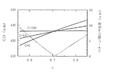
S101では、面積密度U毎に照射量Diとパターン寸法CDiの関係が求められる。具体的には、まず、面積密度Uの異なる複数のパターンを電子ビームの照射量Diを変えて描画し、描画後のパターン寸法CDiを測定して照射量Diとの関係を求める。ここで、複数のDbaseと近接効果補正係数ηの組を用い、D=DbaseDp(η、U)を変えて描画する。例えば、図2のように、面積密度Uが、約0%のラインパターンと、50%のラインパターンと、100%のラインパターンとが組になったパターンセットを配置し、電子ビームの照射量Diの値を変えてマスクに描画する。次いで、描画後の各パターンの線幅寸法CDiを測定する。 In S101, the relationship between the dose D i and the pattern dimension CD i is obtained for each area density U. Specifically, first, a plurality of patterns having different area densities U are drawn while changing the electron beam irradiation amount D i, and the pattern dimension CD i after drawing is measured to obtain the relationship with the irradiation amount D i . Here, using a set of a plurality of D bases and the proximity effect correction coefficient η, D = D base D p (η, U) is changed for rendering. For example, as shown in FIG. 2, a pattern set in which a line pattern having an area density U of about 0%, a line pattern of 50%, and a line pattern of 100% is arranged, and the irradiation amount of the electron beam is arranged. by changing the value of D i is drawn to the mask. Next, the line width dimension CD i of each pattern after drawing is measured.
S102では、実験で用いたDbase毎に最適なηを算出する。具体的には、図3に示すように、あるDbaseでのηと寸法CDの関係を面積密度毎に線形補間して定め、面積密度間の寸法差が最小となるηを最適値とする。このようにして、寸法CDに対する近接効果補正係数ηと基準照射量Dbaseとの相関関係CD(η、Dbase)を算出する。 In S102, the optimum η is calculated for each D base used in the experiment. Specifically, as shown in FIG. 3, the relationship between η and dimension CD in a certain D base is determined by linear interpolation for each area density, and η that minimizes the dimensional difference between the area densities is set as the optimum value. . In this way, the correlation CD (η, D base ) between the proximity effect correction coefficient η and the reference dose D base for the dimension CD is calculated.
S103では、S102で得られた相関関係CD(η、Dbase)をフィッティングする。すなわち、寸法CDとDbaseまたはηの離散的な組を適当な近似式でフィッティングして連続的な値を得る。ここで、本発明におけるフィッティングは、離散的な値に対し、連続的な関数の最良フィッティングパラメータまたは係数を決定するための数学的最適化法として理解される。この用語は、一般に、曲線フィッティング計算についての全ての数学的方法を包含する。こうした曲線フィッティング計算の目的は、データに対して最もよくフィットする関数を導出する点にある。 In S103, the correlation CD (η, D base ) obtained in S102 is fitted. That is, a continuous value is obtained by fitting a discrete set of dimensions CD and D base or η with an appropriate approximate expression. Here, fitting in the present invention is understood as a mathematical optimization method for determining the best fitting parameters or coefficients of a continuous function for discrete values. The term generally encompasses all mathematical methods for curve fitting calculations. The purpose of such curve fitting calculations is to derive the function that best fits the data.
本発明者は、鋭意研究した結果、下記の(1)式をフィッティング関数として選択することにより、S102で得られた寸法CDと近接効果補正係数ηの関係を上手く表現できることを見出した。
η=η0/erfc(ΔCD/2/σF)/2 (1)
ここで、erfcは誤差関数を示す。また、ηは近接効果補正係数、ΔCDはパターン寸法の設計寸法からのずれである。さらに、η0とσFはフィッティングパラメータであって、それぞれ標準の近接効果補正係数と前方散乱の影響範囲を表す。
As a result of diligent research, the present inventor has found that the relationship between the dimension CD obtained in S102 and the proximity effect correction coefficient η can be expressed well by selecting the following equation (1) as a fitting function.
η = η 0 / erfc (ΔCD / 2 / σ F ) / 2 (1)
Here, erfc represents an error function. Further, η is a proximity effect correction coefficient, and ΔCD is a deviation of the pattern dimension from the design dimension. Furthermore, η 0 and σ F are fitting parameters, which respectively represent a standard proximity effect correction coefficient and an influence range of forward scattering.
例えば、石英等の透明ガラス基板上に遮光層となるクロム膜を形成し、さらにクロム膜上にレジスト膜として、富士フィルム株式会社製のレジストFEP−171(商品名)を形成したマスクを用意する。そして、このレジストに対してS101、S102の工程を行う。得られた寸法CDと近接効果補正係数ηの関係は、式(1)のフィッティング関数によって上手く表現される。 For example, a mask in which a chromium film serving as a light shielding layer is formed on a transparent glass substrate such as quartz and a resist FEP-171 (trade name) manufactured by Fuji Film Co., Ltd. is formed as a resist film on the chromium film is prepared. . And the process of S101 and S102 is performed with respect to this resist. The relationship between the obtained dimension CD and the proximity effect correction coefficient η is well expressed by the fitting function of Expression (1).
また、本発明者は、寸法CDと基準照射量Dbaseの関係については、3次多項式によって上手く表現できることを見出した。したがって、S103、S104の工程においては、(a)算出した近接効果補正係数と設計寸法からのずれの離散値を式(1)でフィッティングする、および、(b)算出した設計寸法からのずれと基準照射量の離散値を多項式でフィッティングする、のいずれか一方または両方を行なうことができる。 Further, the present inventor has found that the relationship between the dimension CD and the reference dose D base can be expressed well by a cubic polynomial. Therefore, in the steps S103 and S104, (a) fitting the calculated proximity effect correction coefficient and the discrete value of the deviation from the design dimension with the equation (1), and (b) deviation from the calculated design dimension. Either or both of fitting a discrete value of the reference dose with a polynomial can be performed.
式(1)のフィッティング関数は、パラメータがη0とσのみであり、CD(Dbase)は3次多項式でフィッティングできる。よって、CD(η)、CD(Dbase)の関係に誤差があった場合にフィッティングを用いれば、この誤差を拾って補間するおそれを低減できる。また、CD(η)およびCD(Dbase)の組の数よりパラメータ数の方が十分に少ないと考えられるので、フィッティングする過程でこれらの組に含まれる誤差を低減または平均化できる。さらに、S101で描画した範囲外のCD(η)を外挿して求める場合、線形など単純な外挿に比べ誤差を低減することもできる。尚、S102で得られたCD(η,Dbase)には誤差が含まれていることを考慮すると、フィッティングして得られた値を用いる方が、外挿点付近の数個のデータを1次式等で外挿して得られる値を用いるよりも信頼性に高いと言える。 The fitting function of Expression (1) has only parameters η 0 and σ, and CD (D base ) can be fitted with a cubic polynomial. Therefore, if fitting is used when there is an error in the relationship between CD (η) and CD (D base ), the possibility of interpolating by picking up this error can be reduced. Further, since it is considered that the number of parameters is sufficiently smaller than the number of sets of CD (η) and CD (D base ), errors included in these sets can be reduced or averaged during the fitting process. Furthermore, when extrapolating CD (η) outside the range drawn in S101, the error can be reduced as compared with a simple extrapolation such as linear. In consideration of the fact that the CD (η, D base ) obtained in S102 includes an error, using the value obtained by fitting results in several pieces of data near the extrapolation point being 1 It can be said that the reliability is higher than using a value obtained by extrapolation by the following equation or the like.
S104では、S103のフィッティング結果からCD(η,Dbase)を補間および/または外挿する。尚、本実施の形態では、S103およびS104に代えて、S102で得られた離散的なCD(η,Dbase)をスプライン補間して、CD(η,Dbase)の関係を求めてもよい(S105)。 In S104, CD (η, D base ) is interpolated and / or extrapolated from the fitting result in S103. In the present embodiment, instead of S103 and S104, the discrete CD (η, D base ) obtained in S102 may be spline-interpolated to obtain the relationship of CD (η, D base ). (S105).
次に、S104またはS105の結果からCD(η,Dbase)を定める(S106)。ここで、本実施の形態においては、S102で得られたCD(η,Dbase)をスプライン関数または式(1)等のフィッティング結果から補間し、式(1)の関数を用いてフィッティングした結果を用いて外挿することが好ましい。スプライン関数による補間とフィッティングによる外挿を組合せる場合、両者の相関性を高めるために、適当な重みを付けてフィッティングすることが好ましい。例えば、S102で得られたCD(η,Dbase)の内で、寸法差ΔCDの最大値および最小値に対応するデータの重みを大きくしてフィッティングを行う。これにより、補間と外挿の境界でデータが大きく変動するのを防ぐことができる。 Next, CD (η, D base ) is determined from the result of S104 or S105 (S106). Here, in the present embodiment, the CD (η, D base ) obtained in S102 is interpolated from the fitting result such as the spline function or Expression (1), and the result of fitting using the function of Expression (1). It is preferable to extrapolate using. When combining interpolation by spline function and extrapolation by fitting, it is preferable to perform fitting with an appropriate weight in order to increase the correlation between the two. For example, fitting is performed by increasing the weight of the data corresponding to the maximum value and the minimum value of the dimension difference ΔCD in the CD (η, D base ) obtained in S102. This can prevent the data from fluctuating greatly at the boundary between interpolation and extrapolation.
本実施の形態においては、最小2乗法によるフィッティングや、別の誤差評価関数によるフィッティングを行ってもよい。関数の係数は、全ての値の対の偏差の2乗の和が最小になるように決定される。例えば、
y=a0+a1x+a2x2+a3x3
の3次多項式関数をフィッティング関数として選択する場合、係数a0、a1、a2およびa3は、この関数の曲線ができる限り値の対に近接にフィットするように決定される。富士フィルム株式会社製のレジストPRL−009(商品名)の場合には、フィッティング関数として4次多項式を用いることにより、S102で得られたCD(η,Dbase)を上手く表現できる。尚、データの誤差をフィッティングで拾わないようにするため、フィッティングで使用する式の次数はできるだけ低い方が好ましい。それ故、予め次数の最大値を決めておき、この次数以下でフィッティングできないときには、エラーと判断して描画処理を停止することが好ましい。
In the present embodiment, fitting by the least square method or fitting by another error evaluation function may be performed. The coefficient of the function is determined so that the sum of the squares of the deviations of all value pairs is minimized. For example,
y = a 0 + a 1 x + a 2 x 2 + a 3 x 3
If the third order polynomial function is selected as the fitting function, the coefficients a 0 , a 1 , a 2 and a 3 are determined so that the curve of this function fits as closely as possible to the value pairs. In the case of the resist PRL-009 (trade name) manufactured by Fuji Film Co., Ltd., the CD (η, D base ) obtained in S102 can be expressed well by using a fourth-order polynomial as the fitting function. In order to prevent data errors from being picked up by fitting, it is preferable that the order of the formula used for fitting is as low as possible. Therefore, it is preferable that a maximum value of the order is determined in advance, and if the fitting cannot be performed below this order, it is determined as an error and the drawing process is stopped.
S107では、S106で得られたCD(η,Dbase)を用いて、パターン面積密度50%のラインパターンの照射量D50を算出する。具体的には、D50=DbaseDp(η,U)の関係を用いて求め、(Dbase,η,CD,D50)の関係を求める。尚、上式において、Dpは近接効果補正照射量である。 In S107, CD obtained in S106 (η, D base) is used to calculate the dose D 50 of the pattern area density of 50% of the line pattern. Specifically, the relationship of D 50 = D base D p (η, U) is obtained, and the relationship of (D base , η, CD, D 50 ) is obtained. In the above equation, Dp is the proximity effect correction dose.
S108では、S107で求めた(Dbase,η,CD,D50)の関係から、寸法に対する相関連続線上の近接効果補正係数と基準照射量のうち、50%の面積密度となる線幅1対1のラインパターンにおける照射量がiso−focul doseと一致する近接効果補正係数と基準照射量の組合せ(Dbase,η)を求める。 In S108, from the relationship (D base , η, CD, D 50 ) obtained in S107, a pair of line widths having an area density of 50% of the proximity effect correction coefficient on the correlation continuous line with respect to the dimension and the reference irradiation amount. A combination (D base , η) of the proximity effect correction coefficient and the reference irradiation amount at which the irradiation amount in one line pattern matches the iso-focal dose is obtained.
S108において、(Dbase,η)が所定値以下、すなわち、描画条件の制限内であると判断した場合には、S109に進み、iso−focul doseを用いて(Dbase,η)を算出する(S109)。次いで、S110において、S109で得られた(Dbase,η)を用いたときの面積密度U毎のパターン寸法CDUを予測して、(Dbase,η)の関係を評価する。例えば、実験で得られたDiと寸法CDiの関係を適当に補間してCDUを求める。尚、Dbase、η、照射量のいずれかが所定値を超えている場合には、エラーと判断して描画処理を停止し、不正なパラメータで描画が行われるのを防ぐ。 If it is determined in S108 that (D base , η) is equal to or smaller than a predetermined value, that is, within the limits of the drawing conditions, the process proceeds to S109, and (D base , η) is calculated using iso-focal dose. (S109). Then, in S110, obtained in S109 (D base, η) to predict the pattern dimension CD U per area density U when using, to evaluate the relationship of (D base, η). For example, CD U is obtained by appropriately interpolating the relationship between D i and dimension CD i obtained in the experiment. If any of D base , η, and irradiation dose exceeds a predetermined value, it is determined as an error and the drawing process is stopped to prevent drawing with an incorrect parameter.
図5は、面積密度U毎に、描画した際のパターン寸法と設計寸法とのずれを示した一例である。このグラフは、図4に示す寸法CD毎のDbaseとηの関係から、各寸法CDにおける面積密度毎の照射量Dを算出し、この照射量DとS106で得られた関係とを用いて求められる。尚、この例では、試料として、石英等の透明ガラス基板に遮光層となるクロム膜を形成し、クロム膜上にレジスト膜を形成したマスクを想定している。また、レジスト膜として、富士フィルム株式会社製のレジストFEP−171(商品名)を想定している。図5において、横軸は、基準照射条件における寸法からのずらし幅であり、縦軸は、近接効果補正後の目標寸法から実際の寸法を引いた値である。但し、図5では、レジストの種類に応じた寸法のばらつきを考慮していない。 FIG. 5 is an example showing a deviation between the pattern dimension and the design dimension when drawing for each area density U. FIG. In this graph, the dose D for each area density in each dimension CD is calculated from the relationship between D base and η for each dimension CD shown in FIG. 4, and this dose D and the relationship obtained in S106 are used. Desired. In this example, a mask is assumed in which a chromium film serving as a light shielding layer is formed on a transparent glass substrate such as quartz and a resist film is formed on the chromium film. Moreover, the resist FEP-171 (brand name) by Fuji Film Co., Ltd. is assumed as a resist film. In FIG. 5, the horizontal axis is a shift width from the dimension under the reference irradiation condition, and the vertical axis is a value obtained by subtracting the actual dimension from the target dimension after the proximity effect correction. However, FIG. 5 does not take into account dimensional variations according to the type of resist.
図5を用いて、(Dbase,η)の関係を評価することができる。S111において、設計寸法からのずれが所定値以下であり許容範囲内と判断した場合には、(Dbase,η)の関係を用いて描画工程を行う(S112)。具体的には、基準照射量マップDbase(x,y)と近接効果補正係数マップη(x,y)を作成して、近接効果補正照射量Dp(x,y)を求め、この値から電子ビームの照射量を求める。そして、照射時間を算出して描画工程を行う。尚、S111において、目標寸法からのずれや近接誤差が所定値を超えている場合には、エラーと判断して描画処理を停止し、不正なパラメータで描画が行われるのを防ぐ。 Using FIG. 5, the relationship of (D base , η) can be evaluated. In S111, when it is determined that the deviation from the design dimension is equal to or less than the predetermined value and within the allowable range, the drawing process is performed using the relationship of (D base , η) (S112). Specifically, a reference dose map D base (x, y) and a proximity effect correction coefficient map η (x, y) are created to determine a proximity effect correction dose D p (x, y). The electron beam dose is obtained from the above. Then, the drawing process is performed by calculating the irradiation time. In S111, when the deviation from the target dimension or the proximity error exceeds a predetermined value, it is determined as an error and the drawing process is stopped to prevent drawing with an incorrect parameter.
図1は、ローディング補正を行わず近接効果補正のみを行う場合のフローである。次に、図6を用いて、近接効果補正とローディング補正を行う場合のフローについて説明する。 FIG. 1 is a flow when only proximity effect correction is performed without performing loading correction. Next, a flow when proximity effect correction and loading correction are performed will be described with reference to FIG.
図6において、S201〜S207は、図1のS101〜S107と同様であるため、説明を省略する。 In FIG. 6, S201 to S207 are the same as S101 to S107 of FIG.
S208では、S207で求めた(Dbase,η,CD,D50)の関係から、寸法に対する相関連続線上の近接効果補正係数と基準照射量のうち、50%の面積密度となる線幅1対1のラインパターンにおけるiso−focul doseと一致する近接効果補正係数と基準照射量の組合せと、このときのパターン寸法CDisoとを求める。具体的には、ΔCD=CD−CDisoとして、(Dbase,η,CD)の関係から(Dbase,η,ΔCD)の関係を求める。このとき、CDをΔCDに置き換えるだけでもよいが、(Dbase,η,CD)の関係を補間して(Dbase,η,ΔCD)の関係を求めてもよい。 In S208, from the relationship of (D base , η, CD, D 50 ) obtained in S207, a pair of line widths that has an area density of 50% of the proximity effect correction coefficient on the correlation continuous line with respect to the dimension and the reference irradiation amount. The combination of the proximity effect correction coefficient and the reference irradiation amount that coincides with the iso-focal dose in one line pattern, and the pattern dimension CD iso at this time are obtained. Specifically, as ΔCD = CD-CD iso, ( D base, η, CD) from the relationship of (D base, η, ΔCD) determine the relationship. At this time, CD may be replaced by ΔCD, but the relationship (D base , η, ΔCD) may be obtained by interpolating the relationship (D base , η, CD).
S208において、CD(η,Dbase)と照射量が所定値以下、すなわち、描画条件の制限内であると判断した場合には、S209に進み、iso−focul doseを用いてCD(Dbase,η)を算出する(S209)。次いで、S210において、S209で得られたCD(Dbase,η)を用いたときの面積密度U毎のパターン寸法CDUを予測してCD(η,Dbase)の関係を評価する。例えば、実験で得られたDiと寸法CDiの関係を適当に補間してCDUを求める。尚、CD(η,Dbase)と寸法予測値の差および照射量のいずれかが所定値を超えている場合には、エラーと判断して描画処理を停止し、不正なパラメータで描画が行われるのを防ぐ。 In S208, when it is determined that the CD (η, D base ) and the irradiation amount are equal to or less than the predetermined value, that is, within the limits of the drawing conditions, the process proceeds to S209, and the CD (D base , CD using the iso-focal dose η) is calculated (S209). Next, in S210, the resulting CD (D base, η) at S209 to predict the pattern dimension CD U per area density U when using CD (η, D base) to evaluate the relationship. For example, CD U is obtained by appropriately interpolating the relationship between D i and dimension CD i obtained in the experiment. If any of the difference between the CD (η, D base ) and the predicted dimension value and the irradiation dose exceeds a predetermined value, it is determined as an error and the drawing process is stopped, and drawing is performed with an incorrect parameter. To prevent it.
S210の評価は、図5の関係を用いて行える。そして、S211において、設計寸法からのずれが所定値以下であり許容範囲内と判断した場合には、CD(η,Dbase)の関係を用いて描画工程を行う(S212)。具体的には、基準照射量マップDbase(x,y)と近接効果補正係数マップη(x,y)を作成して、近接効果補正照射量Dp(x,y)を求め、この値から電子ビームの照射量を求める。そして、照射時間を算出して描画工程を行う。尚、S211において、設計寸法からのずれが所定値を超えている場合には、エラーと判断して描画処理を停止し、不正なパラメータで描画が行われるのを防ぐ。 The evaluation of S210 can be performed using the relationship of FIG. If it is determined in S211 that the deviation from the design dimension is equal to or less than the predetermined value and is within the allowable range, a drawing process is performed using the relationship of CD (η, D base ) (S212). Specifically, a reference dose map D base (x, y) and a proximity effect correction coefficient map η (x, y) are created to determine a proximity effect correction dose D p (x, y). The amount of electron beam irradiation is obtained from the above. Then, the drawing process is performed by calculating the irradiation time. In S211, if the deviation from the design dimension exceeds a predetermined value, it is determined as an error and the drawing process is stopped to prevent drawing with an incorrect parameter.
以上のような描画方法により試料を描画することで、補正処理の精度を高めて寸法変動を低減することができる。 By drawing the sample by the drawing method as described above, it is possible to improve the accuracy of the correction process and reduce the dimensional variation.
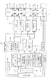
図7は、本実施の形態における電子ビーム描画装置の構成図である。 FIG. 7 is a configuration diagram of the electron beam drawing apparatus according to the present embodiment.
図7に示すように、電子ビーム描画装置は、試料に電子ビームで描画する描画部と、描画を制御する制御部とを有する。試料室1内には、試料であるマスク2が設置されるステージ3が設けられている。マスク2は、例えば、石英等の透明ガラス基板上に、遮光膜としてクロム膜が形成され、さらにこの上にレジスト膜が形成されたものである。本実施の形態では、レジスト膜に対して電子ビームで描画を行う。ステージ3は、ステージ駆動回路4によりX方向(紙面における左右方向)とY方向(紙面における垂直方向)に駆動される。ステージ3の移動位置は、レーザ測長計等を用いた位置回路5により測定される。
As shown in FIG. 7, the electron beam drawing apparatus includes a drawing unit that draws an electron beam on a sample and a control unit that controls drawing. In the
試料室1の上方には、電子ビーム光学系10が設置されている。この光学系10は、電子銃6、各種レンズ7、8、9、11、12、ブランキング用偏向器13、成形偏向器14、ビーム走査用の主偏向器15、ビーム走査用の副偏向器16、および、2個のビーム成型用アパーチャ17、18等から構成されている。
An electron beam
図8は、電子ビームによる描画方法の説明図である。この図に示すように、マスク2上に描画されるパターン51は、短冊状のフレーム領域52に分割されている。電子ビーム54による描画は、ステージ3が一方向(例えば、X方向)に連続移動しながら、フレーム領域52毎に行われる。フレーム領域52は、さらに副偏向領域53に分割されており、電子ビーム54は、副偏向領域53内の必要な部分のみを描画する。尚、フレーム領域52は、主偏向器15の偏向幅で決まる短冊状の描画領域であり、副偏向領域53は、副偏向器16の偏向幅で決まる単位描画領域である。
FIG. 8 is an explanatory diagram of a drawing method using an electron beam. As shown in this figure, the
副偏向領域の基準位置の位置決めは、主偏向器15で行われ、副偏向領域53内での描画は、副偏向器16によって制御される。すなわち、主偏向器15によって、電子ビーム54が所定の副偏向領域53に位置決めされ、副偏向器16によって、副偏向領域53内での描画位置が決められる。さらに、成形偏向器14とビーム成型用アパーチャ17、18によって、電子ビーム54の形状と寸法が決められる。そして、ステージ3を一方向に連続移動させながら、副偏向領域53内を描画し、1つの副偏向領域53の描画が終了したら、次の副偏向領域53を描画する。フレーム領域52内の全ての副偏向領域53の描画が終了したら、ステージ3を連続移動させる方向と直交する方向(例えば、Y方向)にステップ移動させる。その後、同様の処理を繰り返して、フレーム領域52を順次描画して行く。
Positioning of the reference position of the sub deflection area is performed by the
図7で、符号20は入力部であり、記憶媒体である磁気ディスクを通じて電子ビーム描画装置に、マスク2の描画データが入力される部分である。入力部20には、上述した第1のパターンと第2のパターンを電子ビームの照射量を変えて描画した結果や、ローディング効果補正係数γとローディング効果の影響範囲σLのデータ、かぶり効果補正係数θとかぶり効果の影響範囲σiのデータも入力される。
In FIG. 7,
入力部20から読み出された情報に基づき、制御計算機19の第1の算出部において、第1のパターンの寸法と照射量の離散値をフィッティングして連続的な値が得られる。次に、制御計算機19の第2の算出部において、第1の算出部で得られた連続的な値から、面積密度の異なる複数の第1のパターン毎に近接効果補正係数と寸法との関係が求められる。そして、この関係から、第1のパターン間における寸法の差が最小となる近接効果補正係数と、この近接効果補正係数を用いたときのパターンの平均寸法とが求められる。
Based on the information read from the
また、制御計算機19の第3の算出部において、第2のパターンの寸法と照射量の離散値をフィッティングして連続的な値が得られる。次に、制御計算機19の第4の算出部において、第3の算出部で得られた連続的な値から、面積密度の異なる複数の第2のパターン毎にかぶり効果補正係数と寸法との関係が求められ、この関係から第2のパターン間における寸法の差が最小となるかぶり効果補正係数が求められる。そして、後述する照射量算出部31cにおいて、近接効果補正係数とかぶり効果補正係数とを用いて電子ビームの照射量が算出される。
Further, in the third calculation unit of the
入力部20から読み出された描画データは、フレーム領域52毎にパターンメモリ21に一時的に格納される。パターンメモリ21に格納されたフレーム領域52毎のパターンデータ、すなわち、描画位置や描画図形データ等で構成されるフレーム情報は、描画データ補正部31で補正された後、データ解析部であるパターンデータデコーダ22と描画データデコーダ23に送られる。
The drawing data read from the
描画データ補正部31は、ローディング効果補正寸法値算出部31aと、近接効果補正照射量算出部31bと、照射量算出部31cと、照射時間算出部31dと、かぶり効果補正照射量算出部31eとを有する。
The drawing
かぶり効果補正照射量算出部31eは、かぶり効果補正の単位領域毎に、かぶり効果を補正する電子ビームのかぶり効果補正相対照射量Dk(x,y)を算出する。ここで、かぶり効果補正相対照射量Dk(x,y)は、かぶり効果補正の単位領域におけるパターン面積密度Uに依存したパターン密度依存値Df(x,y)と、かぶり効果補正の単位領域のマスク面内位置に依存した位置依存値Dr(x,y)との影響を受ける。パターン密度依存値Df(x,y)は、パターン面積密度U(x,y)、かぶり効果補正係数θ、近接効果補正係数ηとなるマスク面内座標xによる分布関数によって求められる。また、パターン密度依存値Df(x,y)は、次のようにして求められる。例えば、試料として、石英などの透明ガラス基板に遮光層となるクロム膜とレジスト膜とがこの順に形成されたマスクを準備する。そして、このマスクの描画領域に対し、かぶり効果補正単位領域毎に、パターン面積密度が約0%のラインパターンと、50%のラインパターンと、100%のラインパターンとが組になったパターンセットを電子ビームで描画する。次いで、現像処理を行い、得られたレジストパターンの線幅寸法CDを測定する(測定1)。次に、レジストパターンをマスクとしたクロム膜のエッチングにより、クロム膜をパターニングし、得られたクロムパターンの線幅寸法CDを測定する(測定2)。測定1におけるパターンセット位置毎の各面積密度ラインパターンの線幅寸法CDの差を補正するための相対照射量を、マスク面内依存のかぶり効果補正相対照射量(位置依存相対値)Dr(x,y)とすればよい。そして、パターン密度依存値Df(x,y)と位置依存値Dr(x,y)とのかぶり効果補正単位領域毎の積を、各かぶり効果補正単位領域におけるかぶり効果補正相対照射量Dk(x,y)とする。
The fogging effect correction
また、かぶり効果補正照射量算出部31eは、各かぶり効果補正単位領域におけるかぶり効果補正相対照射量Dk(x,y)を、かぶり効果補正単位領域毎のかぶり効果補正相対照射量マップとして作成する。
Further, the fogging effect
ローディング効果補正寸法値算出部31aでは、ローディング効果補正単位領域(第2の領域)におけるローディング効果によるパターン線幅寸法のずれを補正する、ローディング効果補正寸法値CD(x,y)が算出される。次いで、このローディング効果補正寸法値CD(x,y)に基づいて、第2の領域における電子ビームの基準照射量マップが作成される。このマップは、図4に示すCD(η,Dbase)の関係から、ローディング効果補正寸法値CD(x,y)に対応する基準照射量マップDbase(x,y)を求めることにより作成される。
The loading effect correction dimension
また、ローディング効果補正寸法値算出部31aでは、ローディング効果補正単位領域(第2の領域)におけるローディング効果補正寸法値CD(x,y)に基づいて、第2の領域における近接効果補正係数マップが作成される。このマップは、図4に示すCD(η,Dbase)の関係から、ローディング効果補正寸法値CD(x,y)に対応する近接効果補正係数マップη(x,y)を求めることにより作成される。
In addition, the loading effect correction dimension
図4に示すCD(η,Dbase)の関係から、基準照射量マップDbase(x,y)と近接効果補正係数マップη(x,y)を求めることで、任意のパターンに対して同一の寸法値となる補正を実現できる。 By obtaining the reference dose map D base (x, y) and the proximity effect correction coefficient map η (x, y) from the relationship of CD (η, D base ) shown in FIG. It is possible to realize a correction with a dimension value of.
近接効果補正照射量算出部31bでは、ローディング効果補正寸法値算出部31aで求めた基準照射量マップDbase(x,y)と近接効果補正係数マップη(x,y)から、近接効果補正単位領域(第1の領域)における近接効果補正照射量Dpが算出される。
In the proximity effect correction dose calculation unit 31b, the proximity effect correction unit is calculated from the reference dose map D base (x, y) obtained by the loading effect correction dimension
照射量算出部31cでは、実際の照射位置での電子ビームの照射量が算出される。すなわち、かぶり効果補正相対照射量Dk(x,y)と近接効果補正照射量Dpに基づいて、電子ビームの照射量Dが求められる。
In the irradiation
照射時間算出部31dでは、描画領域の各位置における電子ビームの照射時間Tが算出される。ここで、照射量Dは、照射時間Tと電流密度Jの積になるので、照射時間Tは、照射量Dを電流密度Jで徐することにより求められる。
In the irradiation
パターンデータデコーダ22からの情報は、ブランキング回路24とビーム成型器ドライバ25に送られる。具体的には、パターンデータデコーダ22で上記データに基づいたブランキングデータが作成され、ブランキング回路24に送られる。また、所望とするビーム寸法データも作成されて、ビーム成型器ドライバ25に送られる。そして、ビーム成型器ドライバ25から、電子光学系10の成形偏向器14に所定の偏向信号が印加されて、電子ビーム54の寸法が制御される。
Information from the pattern data decoder 22 is sent to a blanking circuit 24 and a
図7の偏向制御部30は、セトリング時間決定部29に接続し、セトリング時間決定部29は、副偏向領域偏向量算出部28に接続し、副偏向領域偏向量算出部28は、パターンデータデコーダ22に接続している。また、偏向制御部30は、ブランキング回路24と、ビーム成型器ドライバ25と、主偏向器ドライバ26と、副偏向器ドライバ27とに接続している。
7 is connected to a settling
描画データデコーダ23の出力は、主偏向器ドライバ26と副偏向器ドライバ27に送られる。そして、主偏向器ドライバ26から、電子光学系10の主偏向部15に所定の偏向信号が印加されて、電子ビーム54が所定の主偏向位置に偏向走査される。また、副偏向器ドライバ27から、副偏向器16に所定の副偏向信号が印加されて、副偏向領域53内での描画が行われる。
The output of the drawing
次に、電子ビーム描画装置による描画方法について説明する。 Next, a drawing method by the electron beam drawing apparatus will be described.
まず、試料室1内のステージ3上にマスク2を載置する。次いで、ステージ3の位置検出を位置回路5により行い、制御計算機19からの信号に基づいて、ステージ駆動回路4によりステージ3を描画可能な位置まで移動させる。
First, the
次に、電子銃6より電子ビーム54を出射する。出射された電子ビーム54は、照明レンズ7により集光される。そして、ブランキング用偏向器13により、電子ビーム54をマスク2に照射するか否かの操作を行う。
Next, an
第1のアパーチャ17に入射した電子ビーム54は、第1のアパーチャ17の開口部を通過した後、ビーム成型器ドライバ25により制御された成形偏向器14によって偏向される。そして、第2のアパーチャ18に設けられた開口部を通過することにより、所望の形状と寸法を有するビーム形状になる。このビーム形状は、マスク2に照射される電子ビーム54の描画単位である。
The
電子ビーム54は、ビーム形状に成形された後、縮小レンズ11によって縮小される。そして、マスク2上における電子ビーム54の照射位置は、主偏向器ドライバ26によって制御された主偏向器15と、副偏向器ドライバ27によって制御された副偏向器16とにより制御される。主偏向器15は、マスク2上の副偏向領域53に電子ビーム54を位置決めする。また、副偏向器16は、副偏向領域53内で描画位置を位置決めする。
The
マスク2への電子ビーム54による描画は、ステージ3を一方向に移動させながら、電子ビーム54を走査することにより行われる。具体的には、ステージ3を一方向に移動させながら、各副偏向領域53内におけるパターンの描画を行う。そして、1つのフレーム領域52内にある全ての副偏向領域53の描画を終えた後は、ステージ3を新たなフレーム領域52に移動して同様に描画する。
Drawing with the
上記のようにして、マスク2の全てのフレーム領域52の描画を終えた後は、新たなマスクに交換し、上記と同様の方法による描画を繰り返す。
After drawing all the
次に、制御計算機19による描画制御について説明する。
Next, drawing control by the
制御計算機19は、入力部20で磁気ディスクに記録されたマスクの描画データを読み出す。読み出された描画データは、フレーム領域52毎にパターンメモリ21に一時的に格納される。
The
パターンメモリ21に格納されたフレーム領域52毎の描画データ、つまり、描画位置や描画図形データ等で構成されるフレーム情報は、描画データ補正部31で上記のようにして補正された後、データ解析部であるパターンデータデコーダ22と描画データデコーダ23を介して、副偏向領域偏向量算出部28、ブランキング回路24、ビーム成型器ドライバ25、主偏向器ドライバ26、副偏向器ドライバ27に送られる。
The drawing data for each
パターンデータデコーダ22では、描画データに基づいてブランキングデータが作成されてブランキング回路24に送られる。また、描画データに基づいて所望とするビーム形状データが作成されて副偏向領域偏向量算出部28とビーム成型器ドライバ25に送られる。
The pattern data decoder 22 generates blanking data based on the drawing data and sends it to the blanking circuit 24. Further, desired beam shape data is created based on the drawing data and is sent to the sub deflection region deflection
副偏向領域偏向量算出部28は、パターンデータデコーダ22により作成したビーム形状データから、副偏向領域53における、1ショットごとの電子ビームの偏向量(移動距離)を算出する。算出された情報は、セトリング時間決定部29に送られ、副偏向による移動距離に対応したセトリング時間が決定される。
The sub deflection region deflection
セトリング時間決定部29で決定されたセトリング時間は、偏向制御部30へ送られた後、パターンの描画のタイミングを計りながら、偏向制御部30より、ブランキング回路24、ビーム成型器ドライバ25、主偏向器ドライバ26、副偏向器ドライバ27のいずれかに適宜送られる。
The settling time determined by the settling
ビーム成型器ドライバ25では、光学系10の成形偏向器14に所定の偏向信号が印加されて、電子ビーム54の形状と寸法が制御される。
In the
描画データデコーダ23では、描画データに基づいて副偏向領域53の位置決めデータが作成され、このデータは主偏向器ドライバ26に送られる。次いで、主偏向器ドライバ26から主偏向器15へ所定の偏向信号が印加されて、電子ビーム54は、副偏向領域53の所定位置に偏向走査される。
The drawing
描画データデコーダ23では、描画データに基づいて、副偏向器16の走査のための制御信号が生成される。制御信号は、副偏向器ドライバ27に送られた後、副偏向器ドライバ27から副偏向器16に所定の副偏向信号が印加される。副偏向領域53内での描画は、設定されたセトリング時間が経過した後、電子ビーム54を繰り返し照射することによって行われる。
The drawing
図9は、本実施の形態における照射量演算方法の流れの一例を示す概念図である。この図は、電子ビーム描画方法の中で、特に、電子ビーム照射量を算出するまでのフローを示している。 FIG. 9 is a conceptual diagram showing an example of the flow of the dose calculation method in the present embodiment. This figure particularly shows a flow until the electron beam irradiation amount is calculated in the electron beam drawing method.
まず、グローバルな領域として、μm〜mmオーダー、例えば、0.5mm〜1mmの寸法でメッシュ状に分割されたかぶり効果補正用の単位領域(第1のメッシュ領域)を定義する。同様に、μm〜mmオーダー、例えば、0.5mm〜1mmの寸法でメッシュ状に分割されたローディング効果補正用の単位領域(第2のメッシュ領域)を定義する。ここでは、一例として、かぶり効果補正用の単位領域とローディング効果補正用の単位領域とを同じ寸法の領域として定義した例について説明する。すなわち、グローバルな領域としてμm〜mmオーダー、例えば、0.5〜1mmの寸法でメッシュ状に分割されたかぶり・ローディング効果補正用の単位領域を定義する。但し、これに限るものではなく、かぶり効果補正用の単位領域とローディング効果補正用の単位領域とを異なる寸法の領域として定義してもよい。また、ローカルな領域として、かぶり効果補正用の単位領域の寸法およびローディング効果補正用の単位領域の寸法よりも小さいμmオーダー、例えば、1μm以下の寸法でメッシュ状に分割された近接効果補正用の単位小領域(第3のメッシュ領域)を定義する。 First, as a global region, a unit region (first mesh region) for fogging effect correction divided in a mesh shape with a size of μm to mm, for example, 0.5 mm to 1 mm is defined. Similarly, a loading effect correction unit region (second mesh region) divided into a mesh shape with a size of μm to mm, for example, 0.5 mm to 1 mm is defined. Here, as an example, a description will be given of an example in which a unit region for fogging effect correction and a unit region for correction of loading effect are defined as regions having the same dimensions. That is, a unit region for fogging / loading effect correction divided into a mesh shape with a size of μm to mm order, for example, 0.5 to 1 mm is defined as a global region. However, the present invention is not limited to this, and the unit area for fogging effect correction and the unit area for loading effect correction may be defined as areas having different dimensions. Further, as a local region, for proximity effect correction divided in a mesh shape in the order of μm smaller than the size of the unit region for fogging effect correction and the unit region for loading effect correction, for example, a size of 1 μm or less. A unit small region (third mesh region) is defined.
上述したように、図7のかぶり効果補正照射量算出部31eは、かぶり・ローディング効果補正単位領域毎に、かぶり効果を補正する荷電粒子ビームのかぶり効果補正相対照射量Dk(x,y)を算出する。具体的には、まず、かぶり・ローディング効果補正単位領域におけるかぶり補正データV(x,y)を計算する。V(x,y)は、図9に示すように、次の式で求められる。
As described above, the fogging effect correction

上述したように、かぶり効果補正相対照射量Dk(x,y)は、かぶり効果補正の単位領域におけるパターン面積密度Uに依存したパターン密度依存値Df(x,y)と、かぶり効果補正の単位領域のマスク面内位置に依存した位置依存値Dr(x,y)との影響を受ける。したがって、パターン密度依存値Df(x,y)と位置依存値Dr(x,y)とのかぶり効果補正単位領域毎の積を、各かぶり効果補正単位領域におけるかぶり効果補正相対照射量Dk(x,y)とする。 As described above, the fogging effect correction relative dose D k (x, y) is equal to the pattern density dependent value D f (x, y) depending on the pattern area density U in the unit area for fogging effect correction, and the fogging effect correction. Is affected by the position-dependent value D r (x, y) depending on the position of the unit area in the mask plane. Therefore, the product of the pattern density dependent value D f (x, y) and the position dependent value D r (x, y) for each fog effect correction unit region is the fog effect correction relative irradiation dose D in each fog effect correction unit region. Let k (x, y).
かぶり効果補正照射量算出部31eは、各かぶり効果補正単位領域におけるかぶり効果補正相対照射量Dk(x,y)に基づいて、かぶり効果補正単位領域毎のかぶり効果補正相対照射量マップを作成する。
The fogging effect correction
図7のローディグ効果補正寸法値算出部31aは、各かぶり・ローディング効果補正単位領域におけるローディング効果によるパターン線幅寸法のずれを補正する補正寸法値CD(x,y)を計算する。ここで、ローディグ効果補正寸法値CD(x,y)は、かぶり・ローディング効果補正単位領域におけるパターン面積密度に依存したパターン密度依存値L(x,y)と、かぶり・ローディング効果補正単位領域のマスク面内位置に依存した位置依存値P(x,y)との影響を受ける。そこで、まず、パターン密度依存のローディグ効果補正寸法値(パタン密度依存値)L(x,y)を計算する。この値は、下記式から求められる。
ローディグ効果補正係数γ、g(x,y)は、ローディング効果の分布関数である。ここでは、g(x,y)は、ローディング効果影響範囲(効果半径)σLのガウス分布で近似できる。ローディング効果半径をcmのオーダーとし、かぶり・ローディング効果補正単位領域をローディング効果半径の10分の1以下とすることで、L(x,y)は次式から求められる。 The loading effect correction coefficient γ, g (x, y) is a distribution function of the loading effect. Here, g (x, y) can be approximated by a Gaussian distribution having a loading effect influence range (effect radius) σ L. By setting the loading effect radius to the order of cm and setting the fogging / loading effect correction unit area to 1/10 or less of the loading effect radius, L (x, y) can be obtained from the following equation.
次に、実験により、位置依存のローディグ効果補正寸法値(位置依存値)P(x,y)を求める。かぶり効果補正相対照射量(位置依存相対値)Dr(x,y)を求める手法を参照して、測定2におけるパターンセット位置毎の線幅寸法CDから測定1におけるパターンセット位置毎の線幅寸法CDを引いた差分値を、位置依存のローディング効果補正寸法値(位置依存値)P(x,y)とすればよい。さらに、このローディング効果補正寸法値はパターンセット位置毎の値であるが、内挿してかぶり・ローディング効果単位領域毎の値となるようにすれば、より高精度なローディング効果補正寸法値P(x,y)を得ることができる。
Next, a position-dependent loadig effect correction dimension value (position-dependent value) P (x, y) is obtained by experiment. With reference to the technique for obtaining the fogging effect corrected relative dose (position-dependent relative value) D r (x, y), the line width at each pattern set position in
パターン面積密度に依存したローディグ効果補正寸法値(パタン密度依存値)L(x,y)と、マスク面内位置に依存したローディグ効果補正寸法値(位置依存値)P(x,y)のかぶり・ローディング効果単位領域毎の和を、各かぶり・ローディング効果補正単位領域におけるローディグ効果補正寸法値CD(x,y)とする。パターン密度依存値だけではなく、位置依存値をも考慮することで、より高精度なローディグ効果補正寸法値を得ることができる。 The fogging effect correction dimension value (pattern density dependent value) L (x, y) depending on the pattern area density and the fogging effect correction dimension value (position dependent value) P (x, y) depending on the position in the mask surface. The sum for each loading effect unit area is defined as a loading effect correction dimension value CD (x, y) in each fogging / loading effect correction unit area. By considering not only the pattern density dependent value but also the position dependent value, a more accurate loadig effect correction dimension value can be obtained.
ここで、かぶり・ローディング効果補正単位領域におけるローディグ効果補正寸法値は、ローディング効果に起因する寸法のみならず、エッチング起因以外のマスク面内不均一を補正するような寸法を加算しても好適である。例えば、現像装置における現像むらによる寸法不均一が挙げられる。 Here, the loading effect correction dimension value in the fogging / loading effect correction unit area is suitable not only for the dimension caused by the loading effect but also by adding a dimension for correcting non-uniformity in the mask surface other than that caused by etching. is there. For example, dimensional non-uniformity due to uneven development in the developing device can be mentioned.
図7のローディグ効果補正寸法値算出部31aは、各かぶり・ローディング効果補正単位領域におけるローディグ効果補正寸法値CD(x,y)に基づいて、各かぶり・ローディング効果補正単位領域における電子ビーム54の基準照射量マップを作成する。このマップは、本実施の形態で得られたCD(η,Dbase)の関係から、ローディグ効果補正寸法値CD(x,y)に対応する基準照射量マップDbase(x,y)を求めて作成される。
The loading effect correction dimension
ローディグ効果補正寸法値算出部31aは、各かぶり・ローディング効果補正単位領域におけるローディグ効果補正寸法値CD(x,y)に基づいて、各かぶり・ローディング効果補正単位領域における近接効果補正係数マップを作成する。このマップは、本実施の形態で得られたCD(η,Dbase)の関係から、ローディグ効果補正寸法値CD(x,y)に対応する近接効果補正係数η(x,y)を求めて作成される。そして、CD(η,Dbase)の関係から、基準照射量マップDbase(x,y)と近接効果補正係数マップη(x,y)を求めることで、任意のパタンカテゴリで同一な寸法値の補正を実現することができる。
The loadig effect correction dimension
図7の近接効果補正照射量算出部31bは、上記の基準照射量マップと近接効果補正係数マップとから、近接効果補正用の単位小領域における近接効果を補正する電子ビーム54の近接効果補正照射量Dpを計算する。そして、実際の照射位置(x,y)での近接効果補正照射量Dpを計算する。ここで、近接効果補正照射量Dpは、実際の照射位置(x,y)を取り囲む周囲の4つの近接効果補正単位領域における近接効果補正照射量Dpを使って内挿計算して求める。
The proximity effect correction dose calculation unit 31b in FIG. 7 corrects the proximity effect correction irradiation of the
尚、本発明は上記実施の形態に限定されるものではなく、本発明の趣旨を逸脱しない範囲内において、種々変形して実施することができる。 The present invention is not limited to the above-described embodiment, and various modifications can be made without departing from the spirit of the present invention.
例えば、本実施の形態で述べた荷電粒子ビーム描画装置は、フィッティングの精度を評価する評価部を有していてもよい。例えば、図7の入力部20に、得られたパラメータを用いて描画した際のパターン寸法と設計寸法を入力する。次いで、評価部において、図5に示すような関係を求める。この関係を基に、フィッティングの精度に問題があると判断した場合には、描画処理を停止する。これにより、予備段階で電子ビームの描画精度を判断することができる。
For example, the charged particle beam drawing apparatus described in this embodiment may include an evaluation unit that evaluates the accuracy of fitting. For example, a pattern dimension and a design dimension when drawing using the obtained parameters are input to the
また、上記実施の形態では電子ビームを用いたが、本発明はこれに限られるものではなく、イオンビームなどの他の荷電粒子ビームを用いた場合にも適用可能である。 In the above embodiment, an electron beam is used. However, the present invention is not limited to this, and the present invention can also be applied to cases where other charged particle beams such as an ion beam are used.
1 試料室
2 マスク
3 ステージ
4 ステージ駆動回路
5 位置回路
6 電子銃
7、8、9、11、12 各種レンズ
10 光学系
13 ブランキング用偏向器
14 成形偏向器
15 主偏向器
16 副偏向器
17 第1のアパーチャ
18 第2のアパーチャ
19 制御計算機
20 入力部
21 パターンメモリ
22 パターンデータデコーダ
23 描画データデコーダ
24 ブランキング回路
25 ビーム成形器ドライバ
26 主偏向器ドライバ
27 副偏向器ドライバ
28 副偏向領域偏向量算出部
29 セトリング時間決定部
30 偏向制御部
31 描画データ補正部
31a ローディング効果補正寸法値算出部
31b 近接効果補正照射量算出部
31c 照射量算出部
31d 照射時間算出部
31e かぶり効果補正照射量算出部
51 描画されるパターン
52 フレーム領域
53 副偏向領域
54 電子ビーム
DESCRIPTION OF
Claims (5)
前記基準照射量毎に、最適な近接効果補正係数と、この近接効果補正係数を用いて描画したときの前記パターンの設計寸法からのずれとを算出する工程と、
算出した前記近接効果補正係数と前記設計寸法からのずれの離散値を下記式でフィッティングする工程と、
η=η0/erfc(ΔCD/2/σF)/2
(但し、erfcは誤差関数、ηは近接効果補正係数、ΔCDは寸法の設計寸法からのずれ、η0とσFはフィッティングパラメータであって、それぞれ標準の近接効果補正係数と前方散乱の影響範囲を表す。)
前記フィッティングした結果を用いて、前記近接効果補正係数と前記設計寸法からのずれを補間および/または外挿する工程とを有することを特徴とする荷電粒子ビーム描画方法。 Drawing a plurality of patterns with different area densities by changing the proximity effect correction coefficient for each reference irradiation amount of the charged particle beam, and measuring the dimension of the pattern after drawing;
Calculating an optimum proximity effect correction coefficient for each reference dose and a deviation from the design dimension of the pattern when drawn using the proximity effect correction coefficient;
Fitting the calculated proximity effect correction coefficient and a discrete value of deviation from the design dimension by the following equation:
η = η 0 / erfc (ΔCD / 2 / σ F ) / 2
(Where erfc is the error function, η is the proximity effect correction coefficient, ΔCD is the deviation of the dimension from the design dimension, η 0 and σ F are the fitting parameters, and the influence range of the standard proximity effect correction coefficient and the forward scattering respectively. Represents.)
A charged particle beam drawing method comprising: interpolating and / or extrapolating the proximity effect correction coefficient and a deviation from the design dimension using the fitting result.
前記近接効果補正係数毎に、この近接効果補正係数を用いて描画したときの前記パターンの設計寸法からのずれと基準照射量とを算出する工程と、
算出した前記設計寸法からのずれと前記基準照射量の離散値を多項式でフィッティングする工程と、
前記フィッティングした結果を用いて、前記設計寸法からのずれと前記基準照射量を補間および/または外挿する工程とを有することを特徴とする荷電粒子ビーム描画方法。 Drawing a plurality of patterns with different area densities by changing the proximity effect correction coefficient for each reference irradiation amount of the charged particle beam, and measuring the dimension of the pattern after drawing;
For each of the proximity effect correction coefficients, calculating a deviation from the design dimension of the pattern and a reference dose when drawing using the proximity effect correction coefficient; and
Fitting the calculated deviation from the design dimension and a discrete value of the reference dose with a polynomial;
A charged particle beam drawing method comprising: a step of interpolating and / or extrapolating the deviation from the design dimension and the reference irradiation amount using the fitting result.
5. The charged particle beam drawing method according to claim 2, wherein the calculated discrete values are weighted for fitting.
Priority Applications (1)
| Application Number | Priority Date | Filing Date | Title |
|---|---|---|---|
| JP2009070946A JP2010225811A (en) | 2009-03-23 | 2009-03-23 | Charged particle beam lithography method |
Applications Claiming Priority (1)
| Application Number | Priority Date | Filing Date | Title |
|---|---|---|---|
| JP2009070946A JP2010225811A (en) | 2009-03-23 | 2009-03-23 | Charged particle beam lithography method |
Publications (1)
| Publication Number | Publication Date |
|---|---|
| JP2010225811A true JP2010225811A (en) | 2010-10-07 |
Family
ID=43042695
Family Applications (1)
| Application Number | Title | Priority Date | Filing Date |
|---|---|---|---|
| JP2009070946A Pending JP2010225811A (en) | 2009-03-23 | 2009-03-23 | Charged particle beam lithography method |
Country Status (1)
| Country | Link |
|---|---|
| JP (1) | JP2010225811A (en) |
Cited By (4)
| Publication number | Priority date | Publication date | Assignee | Title |
|---|---|---|---|---|
| JP2011033932A (en) * | 2009-08-04 | 2011-02-17 | Nuflare Technology Inc | Device and method for drawing charged particle beam |
| JP2016207815A (en) * | 2015-04-21 | 2016-12-08 | 株式会社ニューフレアテクノロジー | Charged particle beam lithography apparatus and charged particle beam lithography method |
| JP2016219829A (en) * | 2016-08-04 | 2016-12-22 | 株式会社ニューフレアテクノロジー | Charged particle beam drawing device and charged particle beam drawing method |
| US10256073B2 (en) | 2017-02-15 | 2019-04-09 | Nuflare Technology, Inc. | Charged particle beam writing method |
-
2009
- 2009-03-23 JP JP2009070946A patent/JP2010225811A/en active Pending
Cited By (4)
| Publication number | Priority date | Publication date | Assignee | Title |
|---|---|---|---|---|
| JP2011033932A (en) * | 2009-08-04 | 2011-02-17 | Nuflare Technology Inc | Device and method for drawing charged particle beam |
| JP2016207815A (en) * | 2015-04-21 | 2016-12-08 | 株式会社ニューフレアテクノロジー | Charged particle beam lithography apparatus and charged particle beam lithography method |
| JP2016219829A (en) * | 2016-08-04 | 2016-12-22 | 株式会社ニューフレアテクノロジー | Charged particle beam drawing device and charged particle beam drawing method |
| US10256073B2 (en) | 2017-02-15 | 2019-04-09 | Nuflare Technology, Inc. | Charged particle beam writing method |
Similar Documents
| Publication | Publication Date | Title |
|---|---|---|
| JP4476975B2 (en) | Charged particle beam irradiation amount calculation method, charged particle beam drawing method, program, and charged particle beam drawing apparatus | |
| JP5204687B2 (en) | Charged particle beam drawing method and charged particle beam drawing apparatus | |
| KR100878970B1 (en) | Charged particle beam writing apparatus | |
| JP5480555B2 (en) | Charged particle beam drawing apparatus and charged particle beam drawing method | |
| JP4976071B2 (en) | Charged particle beam drawing method and charged particle beam drawing apparatus | |
| KR101757743B1 (en) | Flare correction method and method for fabricating EUV(Extreme Ultra Violet) mask | |
| JP4476987B2 (en) | Charged particle beam drawing method, program, and charged particle beam drawing apparatus | |
| JP5731257B2 (en) | Charged particle beam drawing apparatus and charged particle beam drawing method | |
| KR20180107071A (en) | Method for performing dose modulation for electron beam lithography | |
| JP5443548B2 (en) | Pattern creating method and charged particle beam drawing apparatus | |
| JP4747112B2 (en) | Pattern forming method and charged particle beam drawing apparatus | |
| JP5416998B2 (en) | Charged particle beam drawing method and charged particle beam drawing apparatus | |
| JP2010225811A (en) | Charged particle beam lithography method | |
| JP5437124B2 (en) | Charged particle beam drawing method and charged particle beam drawing apparatus | |
| CN110517954B (en) | Electron beam irradiation method, electron beam irradiation apparatus, and computer-readable nonvolatile storage medium having program recorded thereon | |
| JP5547113B2 (en) | Charged particle beam drawing apparatus and charged particle beam drawing method | |
| KR20200141494A (en) | Charged particle beam drawing apparatus, charged particle beam drawing method and program | |
| JP2010147449A (en) | Charged particle lithography method and charged particle lithographic apparatus | |
| US11804361B2 (en) | Charged particle beam writing method, charged particle beam writing apparatus, and computer-readable recording medium | |
| JP2010267723A (en) | Charged particle beam lithography system and charged particle beam lithography method | |
| JP2012044044A (en) | Charged particle beam lithography method | |
| JP4825450B2 (en) | Pattern writing system, charged beam writing method, and photomask manufacturing method | |
| JP2010251580A (en) | Method of manufacturing semiconductor device and exposure apparatus | |
| JP2022177801A (en) | Charged particle beam writing method, charged particle beam writing device, and program |