JP2010219829A - Magnetic coupling type isolator - Google Patents
Magnetic coupling type isolator Download PDFInfo
- Publication number
- JP2010219829A JP2010219829A JP2009063691A JP2009063691A JP2010219829A JP 2010219829 A JP2010219829 A JP 2010219829A JP 2009063691 A JP2009063691 A JP 2009063691A JP 2009063691 A JP2009063691 A JP 2009063691A JP 2010219829 A JP2010219829 A JP 2010219829A
- Authority
- JP
- Japan
- Prior art keywords
- magnetic detection
- magnetic field
- planar coil
- magnetic
- detection element
- Prior art date
- Legal status (The legal status is an assumption and is not a legal conclusion. Google has not performed a legal analysis and makes no representation as to the accuracy of the status listed.)
- Withdrawn
Links
Images
Landscapes
- Hall/Mr Elements (AREA)
- Networks Using Active Elements (AREA)
Abstract
Description
本発明は、平面コイルと磁気検出素子とを備えて構成される磁気結合型アイソレータに関する。 The present invention relates to a magnetically coupled isolator configured to include a planar coil and a magnetic detection element.
下記特許文献には磁気結合型アイソレータに関する発明が開示されている。磁気結合型アイソレータは、入力信号を、磁気に変換するための平面コイルと、前記平面コイルから生じた外部磁界を検出して電気信号に変換するための磁気検出素子とを有して構成される。そして、その電気信号を信号処理回路を介して出力側に伝送して出力を取り出す。 The following patent documents disclose inventions related to magnetically coupled isolators. The magnetically coupled isolator includes a planar coil for converting an input signal into magnetism, and a magnetic detection element for detecting an external magnetic field generated from the planar coil and converting it into an electrical signal. . Then, the electric signal is transmitted to the output side via the signal processing circuit to take out the output.
磁気検出素子としては、ホール素子、AMR素子(異方性磁気検出素子)、あるいは、GMR素子(巨大磁気検出素子)が使用される。 As the magnetic detection element, a Hall element, an AMR element (anisotropic magnetic detection element), or a GMR element (giant magnetic detection element) is used.
従来における磁気結合型アイソレータでは、平面コイルと、磁気検出素子とを高さ方向に絶縁層を介して対向配置していた。 In a conventional magnetically coupled isolator, a planar coil and a magnetic detection element are arranged to face each other via an insulating layer in the height direction.
絶縁層は、平面コイルと磁気検出素子間を電気的に絶縁するが、磁気的には結合させる厚さにしなければならない。したがって絶縁層の膜厚を極端に厚くできず、このとき、絶縁層に高さ方向へのピンホール等が発生すると、磁気検出素子と平面コイル間の絶縁性が低下しやすい問題があった。 The insulating layer electrically insulates between the planar coil and the magnetic sensing element, but must be thick enough to be magnetically coupled. Therefore, the film thickness of the insulating layer cannot be extremely increased. At this time, if a pinhole or the like in the height direction is generated in the insulating layer, there is a problem that the insulation between the magnetic detection element and the planar coil is likely to be lowered.
また例えば磁気検出素子は素子抵抗を高めるためにミアンダ形状で形成されており、平面コイルと磁気検出素子との対向面積は大きくなる。この結果、上記した絶縁性の低下が顕著になり、さらに、平面コイルを有する1次側回路(入力側回路)と、磁気検出素子を有する2次側回路(出力側回路)間の静電容量Cが大きくなり、高速応答性が低下する問題が生じた。 Further, for example, the magnetic detection element is formed in a meander shape in order to increase the element resistance, and the facing area between the planar coil and the magnetic detection element is increased. As a result, the above-described decrease in insulation becomes significant, and further, the capacitance between the primary side circuit (input side circuit) having a planar coil and the secondary side circuit (output side circuit) having a magnetic detection element. C becomes large, resulting in a problem that high-speed response decreases.
そこで本発明は上記従来課題を解決するためのものであり、特に、磁気検出素子と平面コイル間の絶縁性の低下を抑制でき、また、1次側回路と2次側回路間の静電容量Cを従来よりも小さくすることで、より高速伝送できる磁気結合型アイソレータを提供することを目的としている。 Accordingly, the present invention is for solving the above-described conventional problems, and in particular, it is possible to suppress a decrease in insulation between the magnetic detection element and the planar coil, and the capacitance between the primary side circuit and the secondary side circuit. An object of the present invention is to provide a magnetically coupled isolator capable of transmitting at higher speed by making C smaller than the conventional one.
本発明における磁気結合型アイソレータは、
入力信号により外部磁界を発生させるための平面コイルと、前記外部磁界を検出して電気信号に変換するための磁気検出素子と、前記平面コイルと前記磁気検出素子の間に介在する絶縁層と、を有し、
前記磁気検出素子は、前記平面コイルの側方に位置していることを特徴とするものである。これにより、磁気検出素子と平面コイル間の絶縁性の低下を抑制できる。また。磁気検出素子の平面コイルとの対向面積を小さくでき、1次側回路と2次側回路間の静電容量Cを小さくでき、高速応答性を向上させることができる。
The magnetically coupled isolator in the present invention is
A planar coil for generating an external magnetic field in response to an input signal; a magnetic detection element for detecting the external magnetic field and converting it to an electrical signal; an insulating layer interposed between the planar coil and the magnetic detection element; Have
The magnetic detection element is located on a side of the planar coil. Thereby, the fall of the insulation between a magnetic detection element and a planar coil can be suppressed. Also. The area facing the planar coil of the magnetic detection element can be reduced, the capacitance C between the primary side circuit and the secondary side circuit can be reduced, and high-speed response can be improved.
本発明では、前記磁気検出素子は、ホール素子であり、前記磁気検出素子の側面と前記平面コイルの側面とが水平方向にて対向するように配置されていることが好ましい。ホール素子は垂直磁場成分により電気特性が変化するため、ホール素子で形成された磁気検出素子の側面と平面コイルの側面とを水平方向にて対向させることで、磁気検出素子に平面コイルからの垂直磁場成分を適切に作用させ、磁気検出素子により、平面コイルから生じた外部磁界を検出することが出来る。 In the present invention, it is preferable that the magnetic detection element is a Hall element, and is arranged so that a side surface of the magnetic detection element and a side surface of the planar coil face each other in the horizontal direction. Since the electrical characteristics of the Hall element change depending on the vertical magnetic field component, the side surface of the magnetic sensing element formed by the Hall element and the side surface of the planar coil face each other in the horizontal direction so that the magnetic sensing element is perpendicular to the planar coil. An external magnetic field generated from a planar coil can be detected by a magnetic detection element by appropriately applying a magnetic field component.
あるいは本発明では、前記磁気検出素子は、磁気抵抗効果を利用したMR素子であり、前記磁気検出素子は、前記平面コイルよりも上方あるいは下方に位置していることが好ましい。MR素子は水平磁場成分により電気特性が変化するため、MR素子で形成された磁気検出素子を平面コイルよりも上方あるいは下方に配置することで、磁気検出素子に平面コイルからの水平磁場成分を適切に作用させ、磁気検出素子により、平面コイルから生じた外部磁界を検出することが出来る。 Alternatively, in the present invention, it is preferable that the magnetic detection element is an MR element using a magnetoresistive effect, and the magnetic detection element is located above or below the planar coil. Since the MR element changes its electrical characteristics depending on the horizontal magnetic field component, the magnetic detection element formed by the MR element is arranged above or below the planar coil so that the horizontal magnetic field component from the planar coil is appropriately applied to the magnetic detection element. The external magnetic field generated from the planar coil can be detected by the magnetic detection element.
また本発明では、前記磁気検出素子は、平面内にてミアンダ形状で形成されており、あるいは、前記磁気検出素子は、平面の面積よりも側面の面積のほうが小さい形状で形成される形態に好ましく適用できる。 In the present invention, the magnetic detection element is preferably formed in a meander shape in a plane, or the magnetic detection element is preferably formed in a shape in which the area of the side surface is smaller than the area of the plane. Applicable.
また本発明では、前記平面コイルには、前記平面内の一方向に平行に延び、電流の流れる向きが逆向きとなる第1磁界発生部と第2磁界発生部とが設けられており、
前記第1磁界発生部及び前記第2磁界発生部の前記一方向に平面内にて直交する方向の幅寸法は、前記磁気検出素子の幅寸法よりも大きく形成される形態に好ましく適用できる。
In the present invention, the planar coil is provided with a first magnetic field generating unit and a second magnetic field generating unit that extend in parallel with one direction in the plane and in which the direction of current flow is opposite.
The width dimension of the first magnetic field generation unit and the second magnetic field generation unit in the direction orthogonal to the one direction in a plane can be preferably applied to a form in which the width dimension is larger than the width dimension of the magnetic detection element.
また本発明では、前記平面コイルには、前記平面内の一方向に平行に延び、電流の流れる向きが逆向きとなる第1磁界発生部と第2磁界発生部とが設けられており、前記第1磁界発生部及び前記第2磁界発生部の外側に、夫々、前記磁気検出素子が配置されていることが好ましい。 In the present invention, the planar coil is provided with a first magnetic field generating unit and a second magnetic field generating unit that extend in parallel with one direction in the plane and have opposite directions of current flow. It is preferable that the magnetic detection elements are respectively disposed outside the first magnetic field generation unit and the second magnetic field generation unit.
第1磁界発生部からの外部磁界を検出する磁気検出素子と、第2磁界発生部からの外部磁界を検出する磁気検出素子とが互いに干渉しあうのを抑制できる。また配線パターンの形成を容易化できる。 It is possible to prevent the magnetic detection element that detects the external magnetic field from the first magnetic field generation unit and the magnetic detection element that detects the external magnetic field from the second magnetic field generation unit from interfering with each other. In addition, the formation of the wiring pattern can be facilitated.
本発明の磁気結合型アイソレータによれば、磁気検出素子と平面コイル間の絶縁性の低下を抑制でき、また1次側回路と2次側回路間の静電容量を小さくでき、高速応答性を向上させることができる。 According to the magnetic coupling type isolator of the present invention, it is possible to suppress a decrease in insulation between the magnetic detection element and the planar coil, and it is possible to reduce the capacitance between the primary side circuit and the secondary side circuit, thereby achieving high-speed response. Can be improved.
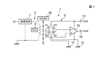
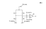
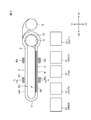
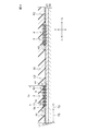
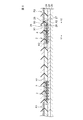
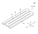
図1は、本実施形態の磁気結合型アイソレータ(磁気カプラ)の全体の回路構成図、図2は、磁気検出素子R1〜R4にて構成されるブリッジ回路図、図3は本実施形態における磁気結合型アイソレータの部分平面図、図4は、図3に示すA−A線に沿って厚さ方向に切断し矢印方向から見た部分拡大断面図、図5は、図4とは異なる形態の磁気結合型アイソレータの部分拡大断面図、図6は、磁気検出素子の斜視図、である。 1 is an overall circuit configuration diagram of a magnetically coupled isolator (magnetic coupler) according to the present embodiment, FIG. 2 is a bridge circuit diagram including magnetic detection elements R1 to R4, and FIG. 3 is a magnetic circuit according to the present embodiment. 4 is a partial plan view of a coupled isolator, FIG. 4 is a partially enlarged cross-sectional view taken along the line AA shown in FIG. 3 and viewed from the direction of the arrow, and FIG. FIG. 6 is a partially enlarged cross-sectional view of a magnetically coupled isolator, and FIG. 6 is a perspective view of a magnetic detection element.
図1に示すように磁気結合型アイソレータ1は、平面コイル2と、磁気検出素子R1〜R4と、平面コイル2と磁気検出素子R1〜R4を電気的に絶縁する絶縁層30とを有して構成される。平面コイル2と各磁気検出素子R1〜R4は磁気的結合が可能な間隔を空けて配置される。
As shown in FIG. 1, the magnetically coupled
平面コイル2は図3のように、X1−X2方向に帯状に延びる第1磁界発生部3と第2磁界発生部4を有する。第1磁界発生部3と第2磁界発生部4は図示Y1−Y2方向に間隔を空けて対向している。第1磁界発生部3と第2磁界発生部4は連結部17,18を介して連結されている。連結部17,18は、湾曲状となっているが形態を限定するものではない。第1磁界発生部3、第2磁界発生部4、及び連結部17,18に囲まれて空間部19が形成されている。
As shown in FIG. 3, the
図4に示すように平面コイル2は、幅寸法T1で形成されたコイル片6が所定の間隔T2を空けて、複数回、平面内にて巻回形成された形状である。よって、図3及び図4に示すように、第1磁界発生部3及び第2磁界発生部4は、X1−X2方向に直線的に延びる複数本のコイル片6がY1−Y2方向に並設された構成となっている。
As shown in FIG. 4, the
平面コイル2に接続される2つの電極パッド5,6が設けられている。電極パッド5,6は円形状であるが特に形状を限定するものではない。さらに平面コイル2は電極パッド5,6を介して図1に示すように送信回路7に接続されている。送信回路7から入力信号に基づく電流が流れると、平面コイル2から外部磁界が発生する。
Two
図4に示すように第1磁界発生部3を構成するコイル片6、及び第2磁界発生部4を構成するコイル片6では電流の流れる向きが反平行である。よって、第1磁界発生部3を構成するコイル片6により発生する外部磁界H1と、第2磁界発生部4を構成するコイル片6により発生する外部磁界H2は逆向きに発生する。
As shown in FIG. 4, in the
図4に示すように、平面コイル2は、基板20上に形成された絶縁下地層21上に形成される。絶縁下地層21はAl2O3やSiO2等で形成される。
As shown in FIG. 4, the
図3,図4に示すように、磁気検出素子R1〜R4が平面コイル2の側方に間隔を空けて配置されている。
As shown in FIGS. 3 and 4, the magnetic detection elements R <b> 1 to R <b> 4 are arranged on the side of the
磁気検出素子R1〜R4は例えばホール素子である。図4に示すように、磁気検出素子R1〜R4は、平面コイル2と同じように絶縁下地層21上に形成される。
The magnetic detection elements R1 to R4 are, for example, Hall elements. As shown in FIG. 4, the magnetic detection elements R <b> 1 to R <b> 4 are formed on the
そして、磁気検出素子R1〜R4上から平面コイル2上にかけて絶縁層30が形成され、各磁気検出素子R1〜R4と平面コイル2間には前記絶縁層30が介在する。磁気検出素子R1〜R4と平面コイル2間の間隔T3(図4参照)は、磁気検出素子R1〜R4と平面コイル2間を電気的には絶縁するが磁気的に結合させる大きさで形成される。絶縁層30の材質は問わない。絶縁層30は無機絶縁材料でも有機絶縁材料でもどちらでもよい。例えば絶縁層30はポリイミドで形成される。
An
図3,図4に示すように、磁気検出素子R1と磁気検出素子R4は、平面コイル2の第1磁界発生部3の外側であってX1−X2方向に間隔を空けて配置されており、磁気検出素子R2と磁気検出素子R3は、平面コイル2の第2磁界発生部4の外側であってX1−X2方向に間隔を空けて配置されている。したがって磁気検出素子R1及び磁気検出素子R4には、第1磁界発生部3より発生する外部磁界H1が作用し、一方、磁気検出素子R2及び磁気検出素子R3には、第2磁界発生部4より発生する外部磁界H2が作用する。
3 and 4, the magnetic detection element R1 and the magnetic detection element R4 are arranged outside the first magnetic
なお図4に示す実施形態では、各磁気検出素子R1〜R4(ホール素子)に全て垂直上方向(あるいは下方向)に磁界が作用する。そこで磁気検出素子R1,R4の組と、磁気検出素子R2,R3の組の一方をn型半導体、他方をp型半導体のホール素子で形成することで、磁界の向きが同一でも、極性を変えることが可能である。 In the embodiment shown in FIG. 4, a magnetic field acts on each of the magnetic detection elements R <b> 1 to R <b> 4 (Hall elements) vertically upward (or downward). Therefore, by forming one of the magnetic detection elements R1 and R4 and the magnetic detection elements R2 and R3 as an n-type semiconductor and the other as a p-type semiconductor Hall element, the polarity is changed even if the direction of the magnetic field is the same. It is possible.
図2に示すように磁気検出素子R1と磁気検出素子R2は直列接続され、磁気検出素子R3と磁気検出素子R4は直列接続されている。 As shown in FIG. 2, the magnetic detection element R1 and the magnetic detection element R2 are connected in series, and the magnetic detection element R3 and the magnetic detection element R4 are connected in series.
図2に示すように磁気検出素子R1と磁気検出素子R3は入力端子(入力パッド)10に接続されている。 As shown in FIG. 2, the magnetic detection element R <b> 1 and the magnetic detection element R <b> 3 are connected to an input terminal (input pad) 10.
また磁気検出素子R2と磁気検出素子R4は夫々、別々のグランド端子(グランドパッド)11,12に接続されている。 The magnetic detection element R2 and the magnetic detection element R4 are connected to separate ground terminals (ground pads) 11 and 12, respectively.
図2に示すように、磁気検出素子R1と磁気検出素子R2の間には第1出力端子(第1出力パッド,OUT1)13が接続されており、磁気検出素子R3と磁気検出素子R4の間には第2出力端子(第2出力パッド,OUT2)14が接続されている。 As shown in FIG. 2, a first output terminal (first output pad, OUT1) 13 is connected between the magnetic detection element R1 and the magnetic detection element R2, and between the magnetic detection element R3 and the magnetic detection element R4. The second output terminal (second output pad, OUT2) 14 is connected to.
図1,図2に示すように、第1出力端子13及び第2出力端子14の出力側が差動増幅器15に接続されている。
As shown in FIGS. 1 and 2, the output sides of the
そして図1に示すように差動増幅器15の出力側は、外部出力端子16に接続されている。
As shown in FIG. 1, the output side of the
図3に示す実施形態では、入力端子10、グランド端子11,12及び出力端子13,14が、平面コイル2から見てY2側に離れた位置に設けられ、各端子10〜14がX1−X2方向に間隔を空けて一列に並んでいる。
In the embodiment shown in FIG. 3, the
そして各磁気検出素子R1〜R4と各端子10〜14間が図示しない配線パターンにより配線され図2に示すブリッジ回路が構成されている。
The magnetic detection elements R1 to R4 and the
各磁気検出素子R1〜R4は、例えば図6に示すように平面内(X−Y平面内)にてミアンダ形状で形成されている。すなわち各磁気検出素子R1〜R4は、X1−X2方向に長く延びる細長部22がY1−Y2方向に所定の間隔を空けて互い違いに連結された形状である。
Each of the magnetic detection elements R1 to R4 is formed in a meander shape in a plane (in the XY plane) as shown in FIG. 6, for example. That is, each of the magnetic detection elements R1 to R4 has a shape in which the
図6に示す各磁気検出素子R1〜R4の平面の面積をS1、側面の面積をS2としたとき、側面の面積S2のほうが平面の面積S1より十分に小さい。側面の面積S2は平面の面積S1に比べて、1/1000〜1/100程度の大きさである。なお平面の面積S1にはX1−X2方向に延びる細長部22間の空間23は含まない。また側面の面積S2は、X1−X2方向に延びる最外側の細長部22におけるX−Z面(X−Z面から傾斜している場合には、その傾斜面)の面積を指す。
When the plane area of each of the magnetic detection elements R1 to R4 shown in FIG. 6 is S1, and the side area is S2, the side area S2 is sufficiently smaller than the plane area S1. The area S2 of the side surface is about 1/1000 to 1/100 of the area S1 of the plane. The planar area S1 does not include the
一方、平面コイル2の第1磁界発生部3及び第2磁界発生部4の平面の面積はS3、側面の面積はS4であり、側面の面積S4のほうが平面の面積S3より小さい。側面の面積S3は平面の面積S4に比べて、1/10〜1/3程度の大きさである。なお、平面の面積S3には、コイル片6間に設けられた間隔T2の面積は含まない。
On the other hand, the plane area of the first
本実施形態では、図4に示すように、各磁気検出素子R1〜R4を、平面コイル2の第1磁界発生部3及び第2磁界発生部4の側方に位置させている。そして絶縁層30が、各磁気検出素子R1〜R4と平面コイル2間に介在する。このため絶縁層30に厚さ方向のピンホール等が生じても、磁気検出素子R1〜R4と平面コイル2間の絶縁性の低下を抑制することが出来る。
In the present embodiment, as shown in FIG. 4, the magnetic detection elements R <b> 1 to R <b> 4 are positioned on the sides of the first magnetic
また本実施形態では、各磁気検出素子R1〜R4を、第1磁界発生部3及び第2磁界発生部4の高さ方向に対向させる場合に比べて、各磁気検出素子R1〜R4の平面コイル2との対向面積を小さくすることができる。
Moreover, in this embodiment, compared with the case where each magnetic detection element R1-R4 is made to oppose the height direction of the 1st magnetic
図3,図4に示すように、平面コイル2の第1磁界発生部3及び第2磁界発生部4のY1−Y2方向への幅寸法T4は、磁気検出素子R1〜R4のY1−Y2方向の幅寸法T5よりも大きい。よって、各磁気検出素子R1〜R4を、平面コイル2の第1磁界発生部3及び第2磁界発生部4と高さ方向にて対向配置した場合、磁気検出素子R1〜R4の平面コイル2との対向面積は、コイル片6間の間隔T2等にもよるが、ほぼ磁気検出素子R1〜R4の平面の面積S1と同等である。一方、各磁気検出素子R1〜R4を、平面コイル2の第1磁界発生部3及び第2磁界発生部4の側方に配置した本実施形態では、磁気検出素子R1〜R4の平面コイル2との対向面積は、最大でも、磁気検出素子R1〜R4の側面の面積S2である。したがって、本実施形態のように、磁気検出素子R1〜R4を平面コイル2の側方に位置させることで従来に比べて十分に平面コイル2との対向面積を減らすことが出来る。
As shown in FIGS. 3 and 4, the width dimension T4 in the Y1-Y2 direction of the first magnetic
図4に示すように、磁気検出素子R1〜R4は平面コイル2の側方に間隔T3を空けて対向し、間隔T3内には絶縁層30が介在する。本実施形態では、磁気検出素子R1〜R4の平面コイル2との対向面積を効果的に小さくできるため、絶縁層30を介した平面コイル2を有する一次側回路8(図1)と、磁気検出素子R1〜R4を有する2次側回路9(図1)間の静電容量Cを小さくでき、高速応答性を向上させることが可能になる。
As shown in FIG. 4, the magnetic detection elements R <b> 1 to R <b> 4 are opposed to the side of the
ここで、平面コイル2の平面の面積S1は、3000〜30000μm2程度であり、側面の面積S2は、300〜3000μm2程度であり、平面コイル2の第1磁界発生部3及び第2磁界発生部4の平面の面積S3は、1000〜10000μm2程度であり、第1磁界発生部3及び第2磁界発生部4の側面の面積S4は、200〜2000μm2程度である。また、平面コイル2のコイル片6の幅寸法T1は、2〜4μm程度、間隔T2は、1〜3μm程度、間隔T3は、5〜20μm程度、第1磁界発生部3及び第2磁界発生部4の幅寸法T4は、30〜80μm程度、磁気検出素子R1〜R4の幅寸法T5は、3〜50μm程度である。
Here, the plane of the area S1 of the
上記したように図4に示す磁気検出素子R1〜R4はホール素子である。ホール素子は、垂直磁場成分により電気特性が変化するため、図4に示すように、磁気検出素子R1〜R4を平面コイル2と同じように絶縁下地層21上に形成し、磁気検出素子R1〜R4を平面コイル2と水平方向(Y1−Y2方向)に対向させることで、磁気検出素子R1〜R4に平面コイル2の第1磁界発生部3及び第2磁界発生部4から垂直磁場成分(Z方向成分)を作用させることが出来る。
As described above, the magnetic detection elements R1 to R4 shown in FIG. 4 are Hall elements. Since the electrical characteristics of the Hall element change depending on the vertical magnetic field component, as shown in FIG. 4, the magnetic detection elements R1 to R4 are formed on the insulating
なお、図4の実施形態では、磁気検出素子R1〜R4と平面コイル2とが水平方向(Y1−Y2方向)に対向していればよいので、磁気検出素子R1〜R4を平面コイル2と同じ形成面上に形成しなくてもよいが、平面コイル2の形成面である絶縁下地層21上に形成することが磁気検出素子R1〜R4の形成を容易化できて好適である。
In the embodiment of FIG. 4, the magnetic detection elements R <b> 1 to R <b> 4 and the
また磁気検出素子R1〜R4の側面の一部が、平面コイル2の側面から上方あるいは下方に多少はみ出した形態を除外しないが、かかる場合、磁気検出素子R1〜R4に作用する垂直磁場成分が弱くなるので、磁気検出素子R1〜R4の側面の全域が、平面コイル2の側面に対向配置されることが好適である。そして、磁気検出素子R1〜R4の側面の全域が、平面コイル2の側面に対向するように、磁気検出素子R1〜R4の高さ寸法L1より平面コイル2の高さ寸法L2を大きく形成したほうがよい。
In addition, a form in which a part of the side surfaces of the magnetic detection elements R1 to R4 protrudes slightly upward or downward from the side surface of the
また図3に示すように、磁気検出素子R1,R4は、X1−X2方向に平行に延びる第1磁界発生部3の外側に配置され、磁気検出素子R2,R3は、第1磁界発生部3と、Y1−Y2方向に空間部19を介して対向し、X1−X2方向に平行に延びる第2磁界発生部4の外側に配置される。これにより、第1磁界発生部3からの外部磁界H1を検出する磁気検出素子R1,R4と、第2磁界発生部4からの外部磁界H2を検出する磁気検出素子R2,R3とが互いに干渉しあうのを抑制できる。また、各磁気検出素子R1〜R4と各端子10〜14間を接続する一部の配線パターンを平面コイル2の外側に引き出して形成できる。
As shown in FIG. 3, the magnetic detection elements R1 and R4 are arranged outside the first magnetic
ただし本実施形態では、空間部19の大きさが磁気検出素子R1〜R4を形成できる程度に大きければ、各磁気検出素子R1〜R4を空間部19内に形成することも可能である。また、一部の磁気検出素子を平面コイル2の外側に、残りの磁気検出素子を平面コイルの内側に配置することも可能である。
However, in this embodiment, if the size of the
図5に示す磁気検出素子R1〜R4は、図4と異なって、磁気抵抗効果(MR効果)を利用したMR素子である。 Magnetic detection elements R1 to R4 shown in FIG. 5 are MR elements using a magnetoresistive effect (MR effect), unlike FIG.
MR素子は、水平磁場成分により電気特性が変化するので、図5に示すように、磁気検出素子R1〜R4を平面コイル2よりも上方、あるいは下方に配置する。
Since the MR element changes its electric characteristics depending on the horizontal magnetic field component, the magnetic detection elements R1 to R4 are arranged above or below the
図5に示すように基板20上に形成された絶縁下地層21上に平面コイル2が形成され、平面コイル2上が第1絶縁層24により覆われている。第1絶縁層24はポリイミド等の有機絶縁材料、あるいは無機絶縁材料で形成される。
As shown in FIG. 5, the
各磁気検出素子R1〜R4は、第1絶縁層24の平面化面24a上であって、平面コイル2の第1磁界発生部3及び第2磁界発生部4の側方に離れた位置に形成される。磁気検出素子R1〜R4は例えば巨大磁気抵抗効果素子(GMR素子)であり、反強磁性層/固定磁性層/非磁性層/フリー磁性層の基本積層構造を備えている。固定磁性層は磁化方向が固定されており例えばY1方向に固定されている。フリー磁性層は磁化が固定されず外部磁界により変動する。
Each of the magnetic detection elements R1 to R4 is formed on the planarized surface 24a of the first insulating
磁気検出素子R1〜R4上は第2絶縁層25にて覆われている。第2絶縁層25は第1絶縁層24と同じ材質であっても異なる材質であってもどちらでも良い。
The magnetic detection elements R1 to R4 are covered with a second insulating
図5に示すように、各磁気検出素子R1〜R4を、平面コイル2の側方であって、平面コイル2から見て上方に位置させることで、各磁気検出素子R1〜R4には、第1磁界発生部3及び第2磁界発生部4からY1−Y2方向の水平磁場成分が作用する。これにより、磁気検出素子R1〜R4の電気特性を変化させることが出来る。
As shown in FIG. 5, each of the magnetic detection elements R1 to R4 is positioned on the side of the
図5の実施形態でも、各磁気検出素子R1〜R4と平面コイル2間の絶縁性を向上させることができる。また、各磁気検出素子R1〜R4の平面コイル2との対向面積を小さくできる。図5の実施形態では、例えば、各磁気検出素子R1〜R4と平面コイル2間が最小距離となる仮想線X0を引く。そして仮想線X0を上下方向に移動させ、仮想線に各磁気検出素子R1〜R4と平面コイル2との双方が接する最大の領域(仮想線X1とX2との間にて対向する領域)を「対向面積」と規定する。また図5の実施形態では、平面コイル2と各磁気検出素子R1〜R4との間の対向距離が一定でない。各磁気検出素子R1〜R4の平面コイル2側を向く側面26と下面27との間の角部28が平面コイル2との距離が最も小さくなる位置であり、この角部28から下面27及び側面26にて離れていくと、平面コイル2との対向距離が徐々に広がっていく。このため、図5の形態において上記のように「対向面積」を規定すると、対向面積は図4の形態に比べて大きくなると考えられるが、実際には各磁気検出素子R1〜R4と平面コイル2間の距離が離れるため、図4と同様、あるいは図4よりも、各磁気検出素子R1〜R4の平面コイル2間に作用する静電容量Cを効果的に小さくできる。
In the embodiment of FIG. 5 as well, the insulation between the magnetic detection elements R1 to R4 and the
図5では、磁気検出素子R1〜R4の下面27が、平面コイル2の上面よりも上方に位置するが、磁気検出素子R1〜R4の下面27と平面コイル2の上面との略同一面である形態も含まれる。ただし磁気検出素子R1〜R4の下面27(あるいは上面)が、平面コイル2の上面(あるいは下面)の上方(あるいは下方)に位置することが、磁気検出素子R1〜R4に、より効果的に水平磁場成分を作用させることができ好適である。
In FIG. 5, the
図5に示す磁気検出素子R1〜R4はGMR素子以外にAMR素子、TMR素子であってもよい。ただしTMR素子の場合は、そもそも素子抵抗が高いので図6に示すミアンダ形状にせず、例えば略円柱状で形成する。 The magnetic detection elements R1 to R4 shown in FIG. 5 may be AMR elements or TMR elements in addition to the GMR elements. However, in the case of a TMR element, since the element resistance is high in the first place, it is not formed in the meander shape shown in FIG.
本実施形態では磁気検出素子R1〜R4の形状を限定するものでないが、ミアンダ形状等、平面の面積よりも側面の面積が小さくなる形態の磁気検出素子を用いる形態に本実施形態の構成を効果的に適用できる。 In the present embodiment, the shape of the magnetic detection elements R1 to R4 is not limited, but the configuration of the present embodiment is effective in a form using a magnetic detection element in which the side surface area is smaller than the planar area, such as a meander shape. Applicable.
R1〜R4 磁気検出素子
1 磁気結合型アイソレータ
2 平面コイル
3 第1磁界発生部
4 第2磁界発生部
8 一次側回路
9 二次側回路
10〜14 端子
19 空間部
24、25、30 絶縁層
R1 to R4
Claims (7)
前記磁気検出素子は、前記平面コイルの側方に位置していることを特徴とする磁気結合型アイソレータ。 A planar coil for generating an external magnetic field in response to an input signal; a magnetic detection element for detecting the external magnetic field and converting it to an electrical signal; an insulating layer interposed between the planar coil and the magnetic detection element; Have
The magnetic coupling type isolator, wherein the magnetic detection element is located on a side of the planar coil.
前記第1磁界発生部及び前記第2磁界発生部の前記一方向に平面内にて直交する方向の幅寸法は、前記磁気検出素子の幅寸法よりも大きく形成されている請求項1ないし5のいずれか1項に記載の磁気結合型アイソレータ。 The planar coil is provided with a first magnetic field generation unit and a second magnetic field generation unit that extend in parallel with one direction in the plane and in which the direction of current flow is opposite.
6. The width dimension of the first magnetic field generation unit and the second magnetic field generation unit in a direction perpendicular to the one direction in a plane is larger than the width dimension of the magnetic detection element. The magnetically coupled isolator according to any one of claims.
Priority Applications (1)
| Application Number | Priority Date | Filing Date | Title |
|---|---|---|---|
| JP2009063691A JP2010219829A (en) | 2009-03-17 | 2009-03-17 | Magnetic coupling type isolator |
Applications Claiming Priority (1)
| Application Number | Priority Date | Filing Date | Title |
|---|---|---|---|
| JP2009063691A JP2010219829A (en) | 2009-03-17 | 2009-03-17 | Magnetic coupling type isolator |
Publications (1)
| Publication Number | Publication Date |
|---|---|
| JP2010219829A true JP2010219829A (en) | 2010-09-30 |
Family
ID=42978183
Family Applications (1)
| Application Number | Title | Priority Date | Filing Date |
|---|---|---|---|
| JP2009063691A Withdrawn JP2010219829A (en) | 2009-03-17 | 2009-03-17 | Magnetic coupling type isolator |
Country Status (1)
| Country | Link |
|---|---|
| JP (1) | JP2010219829A (en) |
-
2009
- 2009-03-17 JP JP2009063691A patent/JP2010219829A/en not_active Withdrawn
Similar Documents
| Publication | Publication Date | Title |
|---|---|---|
| JP6474822B2 (en) | High sensitivity push-pull bridge magnetic sensor | |
| JP5297539B2 (en) | Magnetic sensor | |
| JP6305181B2 (en) | Magnetic sensor | |
| US20130082697A1 (en) | Magnetoresistance sensing device and magnetoresistance sensor including same | |
| JP5899012B2 (en) | Magnetic sensor | |
| JP2008268219A (en) | Magnetic sensor, its manufacturing method, current detecting method, and current detecting device | |
| JP2015194472A (en) | Current detection system | |
| JP2016176911A (en) | Magnetic sensor | |
| JP2012127788A (en) | Magnetic sensor | |
| JP2016535845A (en) | Push-pull bridge type magnetic sensor for high intensity magnetic field | |
| JP2016527503A (en) | Single magnetoresistor TMR magnetic field sensor chip and magnetic currency detector head | |
| JP2013172040A (en) | Magnetic sensor and manufacturing method of the same | |
| WO2009151023A1 (en) | Magnetic sensor and magnetic sensor module | |
| JP5802565B2 (en) | Magnetic sensor | |
| JP2015094732A (en) | Magnetic detector | |
| JP2014089088A (en) | Magnetoresistive effect element | |
| WO2011074488A1 (en) | Magnetic sensor | |
| JP2019035686A (en) | Magnetic sensor | |
| JP5265689B2 (en) | Magnetically coupled isolator | |
| CN103942872B (en) | Magnetic picture identification sensor chip in a kind of low fly height face | |
| JP2018096895A (en) | Magnetic field detection device | |
| JP2010258979A (en) | Magnetic coupling type isolator | |
| JP5413866B2 (en) | Current sensor with magnetic sensing element | |
| JP2009271044A (en) | Current sensor | |
| JP2010258372A (en) | Magnetically coupled isolator |
Legal Events
| Date | Code | Title | Description |
|---|---|---|---|
| A711 | Notification of change in applicant |
Free format text: JAPANESE INTERMEDIATE CODE: A712 Effective date: 20100630 |
|
| RD02 | Notification of acceptance of power of attorney |
Free format text: JAPANESE INTERMEDIATE CODE: A7422 Effective date: 20100728 |
|
| A300 | Application deemed to be withdrawn because no request for examination was validly filed |
Free format text: JAPANESE INTERMEDIATE CODE: A300 Effective date: 20120605 |