JP2010171095A - プリント配線基板 - Google Patents
プリント配線基板 Download PDFInfo
- Publication number
- JP2010171095A JP2010171095A JP2009010539A JP2009010539A JP2010171095A JP 2010171095 A JP2010171095 A JP 2010171095A JP 2009010539 A JP2009010539 A JP 2009010539A JP 2009010539 A JP2009010539 A JP 2009010539A JP 2010171095 A JP2010171095 A JP 2010171095A
- Authority
- JP
- Japan
- Prior art keywords
- wiring pattern
- melting point
- electronic component
- low melting
- pair
- Prior art date
- Legal status (The legal status is an assumption and is not a legal conclusion. Google has not performed a legal analysis and makes no representation as to the accuracy of the status listed.)
- Pending
Links
Images


Landscapes
- Structure Of Printed Boards (AREA)
Priority Applications (1)
| Application Number | Priority Date | Filing Date | Title |
|---|---|---|---|
| JP2009010539A JP2010171095A (ja) | 2009-01-21 | 2009-01-21 | プリント配線基板 |
Applications Claiming Priority (1)
| Application Number | Priority Date | Filing Date | Title |
|---|---|---|---|
| JP2009010539A JP2010171095A (ja) | 2009-01-21 | 2009-01-21 | プリント配線基板 |
Publications (2)
| Publication Number | Publication Date |
|---|---|
| JP2010171095A true JP2010171095A (ja) | 2010-08-05 |
| JP2010171095A5 JP2010171095A5 (enExample) | 2011-08-04 |
Family
ID=42702962
Family Applications (1)
| Application Number | Title | Priority Date | Filing Date |
|---|---|---|---|
| JP2009010539A Pending JP2010171095A (ja) | 2009-01-21 | 2009-01-21 | プリント配線基板 |
Country Status (1)
| Country | Link |
|---|---|
| JP (1) | JP2010171095A (enExample) |
Cited By (1)
| Publication number | Priority date | Publication date | Assignee | Title |
|---|---|---|---|---|
| DE102014115588B4 (de) | 2014-10-27 | 2022-04-28 | Lisa Dräxlmaier GmbH | Sicherungseinrichtung und Verfahren zum Herstellen einer Sicherungseinrichtung |
Citations (2)
| Publication number | Priority date | Publication date | Assignee | Title |
|---|---|---|---|---|
| JPH09161635A (ja) * | 1995-12-14 | 1997-06-20 | S M C:Kk | 温度ヒューズおよびその製造方法 |
| JP2005203686A (ja) * | 2004-01-19 | 2005-07-28 | Funai Electric Co Ltd | プリント配線基板 |
-
2009
- 2009-01-21 JP JP2009010539A patent/JP2010171095A/ja active Pending
Patent Citations (2)
| Publication number | Priority date | Publication date | Assignee | Title |
|---|---|---|---|---|
| JPH09161635A (ja) * | 1995-12-14 | 1997-06-20 | S M C:Kk | 温度ヒューズおよびその製造方法 |
| JP2005203686A (ja) * | 2004-01-19 | 2005-07-28 | Funai Electric Co Ltd | プリント配線基板 |
Cited By (1)
| Publication number | Priority date | Publication date | Assignee | Title |
|---|---|---|---|---|
| DE102014115588B4 (de) | 2014-10-27 | 2022-04-28 | Lisa Dräxlmaier GmbH | Sicherungseinrichtung und Verfahren zum Herstellen einer Sicherungseinrichtung |
Similar Documents
| Publication | Publication Date | Title |
|---|---|---|
| KR102049712B1 (ko) | 퓨즈 엘리먼트, 퓨즈 소자, 및 발열체 내장 퓨즈 소자 | |
| JP6950039B2 (ja) | フレキシブルプリント配線板 | |
| TWI714595B (zh) | 熔絲單元、熔絲元件、保護元件、短路元件、切換元件 | |
| WO2013190604A1 (ja) | 配線基板 | |
| KR20220024892A (ko) | 퓨즈 엘리먼트, 퓨즈 소자 및 보호 소자 | |
| US11013117B2 (en) | Electronic device with built in fuse | |
| JP6408758B2 (ja) | ジャンパー素子 | |
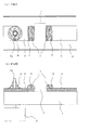
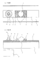
| JP2010171095A (ja) | プリント配線基板 | |
| JP2010073805A (ja) | 回路基板及びその製造方法 | |
| JP2012156195A (ja) | 電子装置 | |
| JP2006222268A (ja) | 電子回路用基板 | |
| JP2016181575A (ja) | 放熱基板及び半導体装置 | |
| KR102706879B1 (ko) | Pcb기판 | |
| JP6306893B2 (ja) | ヒューズ機能付き抵抗器 | |
| JP5428612B2 (ja) | 電子部品の実装構造 | |
| JP5542600B2 (ja) | 半導体モジュール | |
| CN106463313A (zh) | 开关元件、开关电路及警报电路 | |
| JP2010171095A5 (enExample) | ||
| JP6040581B2 (ja) | ヒューズおよびその製造方法 | |
| JP2013178939A (ja) | 電流ヒューズ | |
| JP2007258654A (ja) | 回路基板のランド接続方法及び回路基板 | |
| WO2014034262A1 (ja) | ヒューズ | |
| JP3124191U (ja) | 実装位置ずれ阻止構造を有するプリント配線板 | |
| JP5664527B2 (ja) | 配線基板 | |
| JPH01266784A (ja) | ヒューズ付プリント基板 |
Legal Events
| Date | Code | Title | Description |
|---|---|---|---|
| A521 | Written amendment |
Free format text: JAPANESE INTERMEDIATE CODE: A523 Effective date: 20110620 |
|
| A621 | Written request for application examination |
Effective date: 20110620 Free format text: JAPANESE INTERMEDIATE CODE: A621 |
|
| A977 | Report on retrieval |
Free format text: JAPANESE INTERMEDIATE CODE: A971007 Effective date: 20120619 |
|
| A131 | Notification of reasons for refusal |
Free format text: JAPANESE INTERMEDIATE CODE: A131 Effective date: 20120626 |
|
| A02 | Decision of refusal |
Free format text: JAPANESE INTERMEDIATE CODE: A02 Effective date: 20121113 |