JP2010141982A - Power supply circuit and its operation control method - Google Patents
Power supply circuit and its operation control method Download PDFInfo
- Publication number
- JP2010141982A JP2010141982A JP2008314019A JP2008314019A JP2010141982A JP 2010141982 A JP2010141982 A JP 2010141982A JP 2008314019 A JP2008314019 A JP 2008314019A JP 2008314019 A JP2008314019 A JP 2008314019A JP 2010141982 A JP2010141982 A JP 2010141982A
- Authority
- JP
- Japan
- Prior art keywords
- voltage
- output
- circuit
- input
- power supply
- Prior art date
- Legal status (The legal status is an assumption and is not a legal conclusion. Google has not performed a legal analysis and makes no representation as to the accuracy of the status listed.)
- Granted
Links
- 238000000034 method Methods 0.000 title claims abstract description 10
- 239000003990 capacitor Substances 0.000 claims abstract description 71
- 230000003321 amplification Effects 0.000 claims description 11
- 238000003199 nucleic acid amplification method Methods 0.000 claims description 11
- 230000007423 decrease Effects 0.000 description 29
- 230000010355 oscillation Effects 0.000 description 7
- 230000008859 change Effects 0.000 description 6
- 230000001360 synchronised effect Effects 0.000 description 6
- 238000001514 detection method Methods 0.000 description 4
- 230000004044 response Effects 0.000 description 4
- 239000004065 semiconductor Substances 0.000 description 4
- 238000010586 diagram Methods 0.000 description 3
- 230000003247 decreasing effect Effects 0.000 description 2
- 230000009467 reduction Effects 0.000 description 2
- 230000002441 reversible effect Effects 0.000 description 2
- 230000001052 transient effect Effects 0.000 description 2
- 230000000694 effects Effects 0.000 description 1
- 230000008569 process Effects 0.000 description 1
Images


Abstract
Description
本発明は、小型電子機器に使用する電源回路に関し、特に入力電圧が急変した場合における出力電圧の過渡応答特性を改善することができる電源回路及びその動作制御方法に関する。 The present invention relates to a power supply circuit used for a small electronic device, and more particularly to a power supply circuit capable of improving a transient response characteristic of an output voltage when an input voltage suddenly changes, and an operation control method thereof.
図5は、従来の電源回路の回路例を示した図である(例えば、特許文献1参照。)。
図5の電源回路100では、誤差増幅回路101は所定の基準電圧Vrefと帰還電圧Vfbとの電圧差を増幅して誤差電圧Veを生成し出力する。誤差電圧Veは、利得1のバッファ回路103を介して出力トランジスタM101のゲートに入力される。このため、出力トランジスタM101は、帰還電圧Vfbが基準電圧Vrefに等しくなるように、出力する電流を制御して出力電圧Voutの制御を行う。
FIG. 5 is a diagram showing a circuit example of a conventional power supply circuit (see, for example, Patent Document 1).
In the
すなわち、出力電圧Voutが低下して帰還電圧Vfbが低下すると、誤差増幅回路101からの誤差電圧Veが低下し、出力トランジスタM101のゲート電圧を引き下げる。すると、出力トランジスタM101のオン抵抗が減少し、出力電圧Voutが引き上げられる。逆に、出力電圧Voutが上昇して帰還電圧Vfbが上昇すると、誤差電圧Veが上昇し、出力トランジスタM101のゲート電圧を引き上げる。すると、出力トランジスタM101のオン抵抗が増大し、出力電圧Voutが引き下げられる。このような動作を行うことにより、出力電圧Voutが所定の電圧になるように制御される。出力コンデンサCoは、出力端子OUTに接続された負荷(図示せず)に流れる電流の高周波成分による出力電圧Voutの変動を抑制し、出力電圧Voutを安定させる働きをする。
That is, when the output voltage Vout decreases and the feedback voltage Vfb decreases, the error voltage Ve from the
次に、抵抗R103とコンデンサC101の働きについて説明する。
抵抗R103とコンデンサC101は、入力電圧Vinの急激な変動に対する出力電圧Voutの応答速度を改善する働きを行う。
抵抗R103とコンデンサC101がない場合、入力電圧Vinが急激に低下すると、入力電圧Vinの該低下に応じて直ちに出力トランジスタM101のオン抵抗を小さくしないと、出力電圧Voutが低下するため、出力トランジスタM101のゲート電圧を更に低下させる必要がある。しかし、抵抗R101と演算増幅回路101の非反転入力端とを接続する配線には、図示しないが浮遊容量が存在するため、帰還電圧Vfbは出力電圧Voutの低下よりも遅れて低下する。更に、誤差増幅回路101による遅延も加わり、誤差増幅回路101の出力電圧が低下するまでに時間がかかってしまい、この間に出力電圧Voutは大きく低下してしまう。
Next, functions of the resistor R103 and the capacitor C101 will be described.
The resistor R103 and the capacitor C101 function to improve the response speed of the output voltage Vout with respect to a sudden change in the input voltage Vin.
Without the resistor R103 and the capacitor C101, when the input voltage Vin drops rapidly, the output voltage Vout decreases unless the on-resistance of the output transistor M101 is reduced immediately in response to the drop in the input voltage Vin. It is necessary to further reduce the gate voltage. However, although there is a stray capacitance (not shown) in the wiring connecting the resistor R101 and the non-inverting input terminal of the
このようなことから、抵抗R103とコンデンサC101を追加することにより、入力電圧Vinが急激に低下すると、該電圧低下がコンデンサC101と抵抗R103を介して瞬時に誤差増幅回路101の出力端に伝達されて誤差増幅回路101の出力電圧を低下させる。このため、帰還電圧Vfbの低下を待つことなく、出力トランジスタM101のゲート電圧を低下させることができ、出力電圧Voutの低下を抑制することができる。入力電圧Vinが急激に上昇した場合においては、前記と逆の動作を行うことによって、出力電圧Voutの上昇を抑制することができる。
しかし、図5では、抵抗R103とコンデンサC101の直列回路が、誤差増幅回路101の出力端に接続されているため、コンデンサC101の容量を小さくすることができなかった。抵抗R103とコンデンサC101を追加することによって改善できるのは、入力電圧Vinの変動の高周波成分だけであり、該変動の低周波成分については、帰還電圧Vfbの変化を誤差増幅回路101を介して出力トランジスタM101のゲートに伝えるループ回路で対処することができる。このようなことから、抵抗R103とコンデンサC101で改善させる前記変動の最低周波数は、前記ループ回路で対処することができない周波数以上になるようにすればよい。該周波数は、誤差増幅回路101の周波数特性や、前記配線の浮遊容量等で決まるため個々の回路で異なっていた。
However, in FIG. 5, since the series circuit of the resistor R103 and the capacitor C101 is connected to the output terminal of the
また、コンデンサC101と抵抗R103の直列回路を通して改善することができる入力電圧Vinの過渡応答周波数は、コンデンサC101と抵抗R103の積に反比例することが知られている。このため、より低周波まで改善させるようにするためには、コンデンサC101の容量を大きくするか、又は抵抗R103の抵抗値を大きくすればよいが、電源回路を半導体チップに組み込む場合、コンデンサC101の容量を大きくするとチップ面積が大きくなりコストアップの要因になるため、抵抗R103の抵抗値を大きくする方がよかった。 Further, it is known that the transient response frequency of the input voltage Vin that can be improved through the series circuit of the capacitor C101 and the resistor R103 is inversely proportional to the product of the capacitor C101 and the resistor R103. Therefore, in order to improve the frequency to a lower frequency, the capacitance of the capacitor C101 may be increased or the resistance value of the resistor R103 may be increased. However, when the power supply circuit is incorporated in the semiconductor chip, the capacitor C101 Increasing the capacitance increases the chip area and increases the cost, so it is better to increase the resistance value of the resistor R103.
しかし、抵抗R103には、等価的に誤差増幅回路101の出力インピーダンスが並列に接続されるため、誤差増幅回路101の出力インピーダンス以上の抵抗値には設定することができなかった。また、誤差増幅回路101の出力インピーダンスを大きくすると、誤差増幅回路101による遅延が大きくなり前記ループ回路で制御することができる周波数が低下してしまうため、更にコンデンサC101と抵抗R103の直列回路のハイパス周波数を下げなくてはならず、より低い周波数まで改善させるためにはコンデンサC101の容量を大きくせざるを得なかった。
However, since the output impedance of the
本発明は、このような問題を解決するためになされたものであり、誤差増幅回路101の出力インピーダンスに関係なく、改善可能な入力電圧Vinの変動周波数を任意に設定することができる電源回路及びその動作制御方法を得ることを目的とする。
The present invention has been made to solve such a problem, and a power supply circuit capable of arbitrarily setting a fluctuating frequency of the input voltage Vin that can be improved regardless of the output impedance of the
この発明に係る電源回路は、入力端子から入力された入力電圧を所定の電圧に変換して出力端子から出力電圧として出力する電源回路において、
制御電極に入力された制御信号に応じた動作を行って、前記出力電圧の制御を行う出力トランジスタと、
所定の基準電圧と前記出力電圧に比例した帰還電圧との電圧差を増幅して出力する誤差増幅回路を有し、該誤差増幅回路から出力される誤差電圧を基にして、前記出力電圧が前記所定の電圧で一定になるように前記出力トランジスタの動作制御を行う制御回路部と、
を備え、
前記制御回路部は、前記入力電圧と前記誤差増幅回路の所定の入力端との間に接続されたハイパスフィルタを備えるものである。
A power supply circuit according to the present invention is a power supply circuit that converts an input voltage input from an input terminal into a predetermined voltage and outputs the voltage as an output voltage from an output terminal.
An output transistor for controlling the output voltage by performing an operation in accordance with a control signal input to the control electrode;
An error amplification circuit that amplifies and outputs a voltage difference between a predetermined reference voltage and a feedback voltage proportional to the output voltage, and the output voltage is based on the error voltage output from the error amplification circuit. A control circuit unit for controlling the operation of the output transistor so as to be constant at a predetermined voltage;
With
The control circuit unit includes a high-pass filter connected between the input voltage and a predetermined input terminal of the error amplifier circuit.
具体的には、前記ハイパスフィルタは、コンデンサと抵抗が直列に接続されてなるようにした。 Specifically, the high-pass filter has a capacitor and a resistor connected in series.
また、前記出力トランジスタは、制御電極に入力された制御信号に応じてスイッチングを行い、
前記出力トランジスタのスイッチングによって前記入力電圧による充電が行われるインダクタと、
前記出力トランジスタがオフして遮断状態になったときに前記インダクタの放電を行う整流素子と、
を備え、
前記制御回路部は、前記誤差増幅回路から出力される誤差電圧を基に、前記出力電圧が前記所定の電圧で一定になるように前記出力トランジスタのスイッチング制御を行うようにした。
The output transistor performs switching according to a control signal input to the control electrode,
An inductor charged by the input voltage by switching the output transistor;
A rectifying element that discharges the inductor when the output transistor is turned off and is in a cutoff state;
With
The control circuit unit performs switching control of the output transistor so that the output voltage becomes constant at the predetermined voltage based on the error voltage output from the error amplifier circuit.
この場合、前記制御回路部は、前記入力電圧を降圧して前記出力電圧が前記所定の電圧で一定になるように前記出力トランジスタのスイッチング制御を行うようにした。 In this case, the control circuit unit performs switching control of the output transistor so that the input voltage is stepped down so that the output voltage becomes constant at the predetermined voltage.
また、前記制御回路部は、前記入力電圧を昇圧して前記出力電圧が前記所定の電圧で一定になるように前記出力トランジスタのスイッチング制御を行うようにしてもよい。 The control circuit unit may boost the input voltage and perform switching control of the output transistor so that the output voltage becomes constant at the predetermined voltage.
また、前記制御回路部は、前記入力電圧を変換して前記出力電圧が所定の負電圧で一定になるように前記出力トランジスタのスイッチング制御を行うようにしてもよい。 Further, the control circuit unit may convert the input voltage and perform switching control of the output transistor so that the output voltage becomes constant at a predetermined negative voltage.
また、前記出力トランジスタは、制御電極に入力された制御信号に応じた電流を前記入力端子から前記出力端子に出力し、前記制御回路部は、前記誤差増幅回路から出力された誤差電圧を前記出力トランジスタの制御電極に出力するようにした。 The output transistor outputs a current corresponding to a control signal input to a control electrode from the input terminal to the output terminal, and the control circuit unit outputs the error voltage output from the error amplifier circuit. Output to the control electrode of the transistor.
また、この発明に係る電源回路の動作制御方法は、制御電極に入力された制御信号に応じた動作を行って、出力端子から出力する出力電圧の制御を行う出力トランジスタを備え、入力端子から入力された入力電圧を所定の電圧に変換して前記出力端子から出力する電源回路の動作制御方法において、
所定の基準電圧と前記出力電圧に比例した帰還電圧との電圧差を増幅して出力する誤差増幅回路から出力される誤差電圧を基にして、前記出力電圧が前記所定の電圧で一定になるように前記出力トランジスタの動作制御を行い、
ハイパスフィルタを介して、前記入力電圧の電圧変動を前記誤差増幅回路の所定の入力端に入力するようにした。
In addition, the operation control method of the power supply circuit according to the present invention includes an output transistor that performs an operation according to a control signal input to the control electrode and controls an output voltage output from the output terminal, and is input from the input terminal. In the operation control method of the power supply circuit that converts the input voltage thus converted into a predetermined voltage and outputs it from the output terminal,
Based on an error voltage output from an error amplifier circuit that amplifies and outputs a voltage difference between a predetermined reference voltage and a feedback voltage proportional to the output voltage, the output voltage becomes constant at the predetermined voltage. To control the operation of the output transistor,
The voltage fluctuation of the input voltage is input to a predetermined input terminal of the error amplifier circuit via a high pass filter.
本発明の電源回路及びその動作制御方法によれば、所定の基準電圧と前記出力電圧に比例した帰還電圧との電圧差を増幅する誤差増幅回路から出力される誤差電圧を基にして、前記出力電圧が前記所定の電圧で一定になるように前記出力トランジスタの動作制御を行い、ハイパスフィルタを介して、前記入力電圧の電圧変動を前記誤差増幅回路の所定の入力端に入力するようにしたことから、誤差増幅回路の出力インピーダンスに関係なく、改善可能な入力電圧の変動周波数を任意に設定することができると共に、ハイパスフィルタを構成している抵抗とコンデンサの内、該コンデンサの容量を小さくすることができ、IC化する際に、半導体チップの面積を小さくすることができ、コストの低減を図ることができる。 According to the power supply circuit and the operation control method thereof of the present invention, the output is based on the error voltage output from the error amplification circuit that amplifies the voltage difference between the predetermined reference voltage and the feedback voltage proportional to the output voltage. The operation of the output transistor is controlled so that the voltage becomes constant at the predetermined voltage, and the voltage fluctuation of the input voltage is input to a predetermined input terminal of the error amplifier circuit via a high-pass filter. Therefore, it is possible to arbitrarily set the fluctuating frequency of the input voltage that can be improved regardless of the output impedance of the error amplifier circuit, and to reduce the capacitance of the capacitor and the resistor constituting the high-pass filter. Therefore, when an IC is formed, the area of the semiconductor chip can be reduced, and the cost can be reduced.
次に、図面に示す実施の形態に基づいて、本発明を詳細に説明する。
第1の実施の形態.
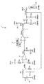
図1は、本発明の第1の実施の形態における電源回路の回路例を示した図である。
図1において、電源回路1は、入力端子INに入力された入力電圧Vinを所定の定電圧に昇圧し、出力電圧Voutとして出力端子OUTから出力する非同期整流型の昇圧型スイッチングレギュレータをなしている。
電源回路1は、NMOSトランジスタからなる出力トランジスタM1と、整流用のダイオードD1とを備えている。
Next, the present invention will be described in detail based on the embodiments shown in the drawings.
First embodiment.
FIG. 1 is a diagram showing a circuit example of a power supply circuit according to the first embodiment of the present invention.
In FIG. 1, a power supply circuit 1 is an asynchronous rectification type boosting switching regulator that boosts an input voltage Vin input to an input terminal IN to a predetermined constant voltage and outputs the boosted voltage from an output terminal OUT as an output voltage Vout. .
The power supply circuit 1 includes an output transistor M1 formed of an NMOS transistor and a rectifying diode D1.
更に、電源回路1は、基準電圧発生回路2と、出力電圧検出用の抵抗R1,R2と、インダクタL1と、出力コンデンサCoと、ハイパスフィルタを形成するコンデンサC1及び抵抗R3と、コンデンサC2と、位相補償用の抵抗R4及びコンデンサC3と、誤差増幅回路3と、発振回路4と、PWMコンパレータ5と、バッファ回路6とを備えている。なお、図1では、スイッチングトランジスタM1が出力トランジスタを、ダイオードD1が整流素子をそれぞれなし、基準電圧発生回路2、抵抗R1〜R4、誤差増幅回路3、発振回路4、PWMコンパレータ5、バッファ回路6及びコンデンサC1〜C3は制御回路部をなす。また、電源回路1において、インダクタL1及び出力コンデンサCoを除く各回路を1つのICに集積するようにしてもよく、場合によっては、スイッチングトランジスタM1及びダイオードD1の少なくとも一方、インダクタL1並びに出力コンデンサCoを除く各回路を1つのICに集積するようにしてもよい。
Furthermore, the power supply circuit 1 includes a reference voltage generation circuit 2, output voltage detection resistors R1 and R2, an inductor L1, an output capacitor Co, a capacitor C1 and a resistor R3 that form a high-pass filter, a capacitor C2, A phase compensation resistor R4 and capacitor C3, an
基準電圧発生回路2は、所定の基準電圧Vrefを生成して出力し、出力電圧検出用の抵抗R1,R2は、出力電圧Voutを分圧して帰還電圧Vfbを生成し出力する。また、誤差増幅回路3は、入力された帰還電圧Vfbと基準電圧Vrefとの電圧差を増幅して誤差電圧Veを生成し出力する。
また、発振回路4は、所定の三角波信号TWを生成して出力し、PWMコンパレータ5は、誤差増幅回路3からの誤差電圧Veと該三角波信号TWからPWM制御を行うためのパルス信号Spwを生成して出力する。パルス信号Spwは、バッファ回路6を介して出力トランジスタM1のゲートに入力される。
The reference voltage generation circuit 2 generates and outputs a predetermined reference voltage Vref, and the output voltage detection resistors R1 and R2 divide the output voltage Vout to generate and output a feedback voltage Vfb. The
The oscillation circuit 4 generates and outputs a predetermined triangular wave signal TW, and the
入力端子INと出力トランジスタM1のドレインとの間にはインダクタL1が接続され、出力トランジスタM1のソースは接地電圧GNDに接続されている。また、インダクタL1と出力トランジスタM1との接続部にはダイオードD1のアノードが接続され、ダイオードD1のカソードは出力端子OUTに接続されている。出力端子OUTと接地電圧GNDとの間には、出力コンデンサCoが接続されると共に、抵抗R2及びR1が直列に接続され、抵抗R2には、コンデンサC2が並列に接続されている。誤差増幅回路3において、反転入力端には帰還電圧Vfbが、非反転入力端には基準電圧Vrefがそれぞれ入力され、出力端は、PWMコンパレータ5の非反転入力端に接続されている。
An inductor L1 is connected between the input terminal IN and the drain of the output transistor M1, and the source of the output transistor M1 is connected to the ground voltage GND. Further, the anode of the diode D1 is connected to the connection portion between the inductor L1 and the output transistor M1, and the cathode of the diode D1 is connected to the output terminal OUT. An output capacitor Co is connected between the output terminal OUT and the ground voltage GND, resistors R2 and R1 are connected in series, and a capacitor C2 is connected in parallel to the resistor R2. In the
入力電圧Vinと誤差増幅回路3の反転入力端との間には、コンデンサC1と抵抗R3の直列回路からなるハイパスフィルタが接続されている。また、誤差増幅回路3の出力端と接地電圧GNDとの間には、抵抗R4及びコンデンサC3の直列回路が接続されている。PWMコンパレータ5の反転入力端には三角波信号TWが入力され、PWMコンパレータ5から出力されたパルス信号Spwは、バッファ回路6を介して出力トランジスタM1のゲートに入力される。
Between the input voltage Vin and the inverting input terminal of the
このように、誤差増幅回路3は、基準電圧Vrefと帰還電圧Vfbとの電圧差を増幅して誤差電圧Veを生成しPWMコンパレータ5の非反転入力端に出力する。PWMコンパレータ5の反転入力端には発振回路4からの三角波信号TWが入力されており、PWMコンパレータ5は、三角波信号TWの電圧が誤差電圧Ve未満の場合はハイレベルの信号を出力し、三角波信号TWの電圧が誤差電圧Ve以上である場合はローレベルの信号を出力する。すなわち、PWMコンパレータ5は、誤差電圧Veに応じて出力するパルス信号Spwのデューティサイクルを変化させる。
Thus, the
出力トランジスタM1は、ゲートがハイレベルのときはオンして導通状態になり、ゲートがローレベルのときはオフして遮断状態になる。出力トランジスタM1がオンしているときは、入力端子INからインダクタL1と出力トランジスタM1を通って接地電圧GNDに電流が流れ、インダクタL1にエネルギーが蓄積される。出力トランジスタM1がオフすると、インダクタL1と出力トランジスタM1との接続部の電圧は、インダクタL1の逆起電力の影響で入力電圧Vinよりも高い電圧になる。また、インダクタL1に蓄積されたエネルギーが、ダイオードD1を介して出力コンデンサCoを充電すると共に出力端子OUTに接続された負荷20に供給される。
The output transistor M1 is turned on when the gate is at a high level and becomes conductive, and is turned off when the gate is at a low level. When the output transistor M1 is on, a current flows from the input terminal IN to the ground voltage GND through the inductor L1 and the output transistor M1, and energy is stored in the inductor L1. When the output transistor M1 is turned off, the voltage at the connection between the inductor L1 and the output transistor M1 becomes higher than the input voltage Vin due to the influence of the counter electromotive force of the inductor L1. Further, the energy stored in the inductor L1 is charged to the output capacitor Co through the diode D1 and supplied to the
出力電圧Voutが低下して帰還電圧Vfbが低下すると、誤差増幅回路3からの誤差電圧Veが上昇する。誤差電圧VeはPWMコンパレータ5の非反転入力端に入力されているため、誤差電圧Veが上昇するとPWMコンパレータ5から出力されたパルス信号Spwのハイレベルの時間が長くなると共にローレベルの時間が短くなる。このため、出力トランジスタM1がオンする時間が長くなってインダクタL1に蓄えられるエネルギーが増加することから、出力電圧Voutは上昇する。逆に、出力電圧Voutが上昇して帰還電圧Vfbが上昇すると、誤差電圧Veが低下する。すると、PWMコンパレータ5から出力されるパルス信号Spwのハイレベルの時間が短くなると共にローレベルの時間が長くなる。このため、出力トランジスタM1がオンする時間が短くなり、インダクタL1に蓄えられるエネルギーも減少することから、出力電圧Voutは低下する。このような動作を繰り返すことにより、出力電圧Voutは所定の電圧に維持される。
When the output voltage Vout decreases and the feedback voltage Vfb decreases, the error voltage Ve from the
一方、コンデンサC1と抵抗R3からなるハイパスフィルタがない場合、前記のように出力電圧Voutの変化を捉えてループ制御を行っているときは、制御に時間がかかり入力電圧Vinの変化に対して高速な応答を行うことができない。このため、出力電圧Voutの高周波成分の変動に対しては、出力コンデンサCoに高周波特性の良いコンデンサを使用することにより対処することができるが、入力電圧Vinの高周波成分の変動に対しては対処することができず、出力電圧Voutが大きく変動してしまう。このため、電源回路1では、入力電圧Vinと誤差増幅回路3の反転入力端との間に、コンデンサC1と抵抗R3の直列回路からなるハイパスフィルタを設けている。
On the other hand, when there is no high-pass filter composed of the capacitor C1 and the resistor R3, when the loop control is performed by capturing the change in the output voltage Vout as described above, the control takes time and the change in the input voltage Vin is fast. Can't respond properly. For this reason, fluctuations in the high-frequency component of the output voltage Vout can be dealt with by using a capacitor having good high-frequency characteristics as the output capacitor Co. However, fluctuations in the high-frequency component of the input voltage Vin are dealt with. The output voltage Vout greatly fluctuates. For this reason, in the power supply circuit 1, a high-pass filter including a series circuit of the capacitor C1 and the resistor R3 is provided between the input voltage Vin and the inverting input terminal of the
前記のようなハイパスフィルタは、入力電圧Vinの変動の内、高周波成分のみを誤差増幅回路3の反転入力端に伝達する。このため、入力電圧Vinが変動すると、出力電圧Voutが変化する前に誤差増幅回路3の反転入力端の電圧を変動させることができる。今、入力電圧Vinが急激に低下したとすると、入力電圧Vinの該変化分は、コンデンサC1と抵抗R3を介して誤差増幅回路3の反転入力端に伝えられ、反転入力端の電圧が低下する。すると、誤差電圧Veが上昇してPWMコンパレータ5から出力されるパルス信号Spwのハイレベルの時間が増加し出力電圧Voutを上昇させるため、入力電圧Vinの急激な低下に対して高速に応答することができる。また、入力電圧Vinが急激に上昇した場合は、前記とまったく逆の動作を行って出力電圧Voutを低下させることができ、やはり高速に応答することができる。
The high-pass filter as described above transmits only a high-frequency component in the fluctuation of the input voltage Vin to the inverting input terminal of the
従来技術の場合と異なり、誤差増幅回路3の入力インピーダンスは極めて大きいため、コンデンサC1と抵抗R3からなるハイパスフィルタの周波数特性に影響を与えることはない。なお、抵抗R3には等価的に抵抗R1とR2を並列に接続した抵抗値が並列に接続されるが、これらの抵抗の抵抗値を高抵抗に設定することができるため、抵抗R3の抵抗値を大きい値に設定することができ、その分コンデンサC1の容量を小さくすることができることから、半導体チップの面積を小さくしてチップのコストを低減させることができる。また、前記説明では省略したが、抵抗R4とコンデンサC3の直列回路は誤差増幅回路3の位相補償を行っており、コンデンサC2は出力電圧Voutの変動を高速に帰還するための働きを行っている。
Unlike the case of the prior art, since the input impedance of the
ここで、図1では電源回路1が昇圧型スイッチングレギュレータをなす場合を例にして示したが、降圧型スイッチングレギュレータをなすようにしてもよく、このようにした場合、図1の電源回路1は図2のようになる。なお、図2では、図1と同じもの又は同様のものは同じ符号で示し、ここではその説明を省略すると共に図1との相違点のみ説明する。
図2における図1との相違点は、図1の出力トランジスタM1をPMOSトランジスタに代えると共に図1のバッファ回路6をインバータ回路7に代え、出力トランジスタM1、ダイオードD1及びインダクタL1の接続を変えたことにある。
Here, FIG. 1 shows an example in which the power supply circuit 1 forms a step-up switching regulator. However, the power supply circuit 1 in FIG. 1 may be formed as a step-down switching regulator. As shown in FIG. 2 that are the same as or similar to those in FIG. 1 are denoted by the same reference numerals, and description thereof is omitted here, and only differences from FIG. 1 are described.
2 differs from FIG. 1 in that the output transistor M1 in FIG. 1 is replaced with a PMOS transistor, the
図2の電源回路1は、入力端子INに入力された入力電圧Vinを所定の定電圧に降圧し、出力電圧Voutとして出力端子OUTから出力する非同期整流型の降圧型スイッチングレギュレータをなしている。
図2の電源回路1は、PMOSトランジスタからなる出力トランジスタM1と、ダイオードD1と、基準電圧発生回路2と、出力電圧検出用の抵抗R1,R2と、インダクタL1と、出力コンデンサCoと、ハイパスフィルタを形成するコンデンサC1及び抵抗R3と、コンデンサC2と、位相補償用の抵抗R4及びコンデンサC3と、誤差増幅回路3と、発振回路4と、PWMコンパレータ5と、インバータ回路7とを備えている。
The power supply circuit 1 of FIG. 2 is an asynchronous rectification step-down switching regulator that steps down the input voltage Vin input to the input terminal IN to a predetermined constant voltage and outputs the voltage as an output voltage Vout from the output terminal OUT.
2 includes an output transistor M1, which is a PMOS transistor, a diode D1, a reference voltage generation circuit 2, resistors R1 and R2 for output voltage detection, an inductor L1, an output capacitor Co, and a high-pass filter. Capacitor C1 and resistor R3, capacitor C2, phase compensation resistor R4 and capacitor C3,
なお、図2の電源回路1では、スイッチングトランジスタM1が出力トランジスタを、ダイオードD1が整流素子をそれぞれなし、基準電圧発生回路2、抵抗R1〜R4、誤差増幅回路3、発振回路4、PWMコンパレータ5、インバータ回路7及びコンデンサC1〜C3は制御回路部をなす。また、図2においても、インダクタL1及び出力コンデンサCoを除く各回路を1つのICに集積するようにしてもよく、場合によっては、スイッチングトランジスタM1及びダイオードD1の少なくとも一方、インダクタL1並びに出力コンデンサCoを除く各回路を1つのICに集積するようにしてもよい。
In the power supply circuit 1 of FIG. 2, the switching transistor M1 is an output transistor, the diode D1 is a rectifying element, a reference voltage generating circuit 2, resistors R1 to R4, an
入力端子INとダイオードD1のカソードとの間には出力トランジスタM1が接続され、ダイオードD1のアノードは接地電圧GNDに接続されている。出力トランジスタM1とダイオードD1との接続部と出力端子OUTとの間にはインダクタL1が接続されている。PWMコンパレータ5の出力端はインバータ回路7を介して出力トランジスタM1のゲートに接続されている。
The output transistor M1 is connected between the input terminal IN and the cathode of the diode D1, and the anode of the diode D1 is connected to the ground voltage GND. An inductor L1 is connected between the connection portion of the output transistor M1 and the diode D1 and the output terminal OUT. The output terminal of the
このような構成において、出力トランジスタM1は、ゲートがローレベルのときはオンして導通状態になり、ゲートがハイレベルのときはオフして遮断状態になる。出力トランジスタM1がオンしているときは、入力端子INから出力トランジスタM1とインダクタL1を介して出力コンデンサCoを充電すると共に出力端子OUTに接続された負荷20に電流を供給する。このときインダクタL1にエネルギーが蓄えられる。出力トランジスタM1がオフすると接地電圧GNDからインダクタL1を介して電流が流れ、インダクタL1に蓄えられていたエネルギーが出力端子OUTから放出される。
In such a configuration, the output transistor M1 is turned on when the gate is at a low level and is turned on, and is turned off and turned off when the gate is at a high level. When the output transistor M1 is on, the output capacitor Co is charged from the input terminal IN through the output transistor M1 and the inductor L1, and current is supplied to the
ここで、出力電圧Voutが低下して帰還電圧Vfbも低下すると、誤差増幅回路3からの誤差電圧Veが上昇する。誤差電圧VeはPWMコンパレータ5の非反転入力端に入力されているため、誤差電圧Veが上昇するとPWMコンパレータ5から出力された信号のハイレベルである時間が長くなり、ローレベルである時間が短くなる。PWMコンパレータ5の出力信号がハイレベルのときは、該ハイレベルの出力信号はインバータ回路7でローレベルに反転されて出力トランジスタM1のゲートに入力され、出力トランジスタM1はオンする。
Here, when the output voltage Vout decreases and the feedback voltage Vfb also decreases, the error voltage Ve from the
逆に、PWMコンパレータ5の出力信号がローレベルである場合は、出力トランジスタM1はオフする。すなわち、出力電圧Voutが低下した場合は、出力トランジスタM1のオンデューティサイクルが大きくなり、インダクタL1に蓄えられるエネルギーが増加するため出力電圧Voutは上昇する。逆に、出力電圧Voutが上昇すると、出力トランジスタM1のオンデューティサイクルが小さくなり、インダクタL1に蓄えられるエネルギーが減少するため、出力電圧Voutは低下する。これ以外の各回路の動作は図1の場合と同様であるのでその説明を省略する。
Conversely, when the output signal of the
また、本発明は反転型スイッチングレギュレータにも適用することができ、この場合、図3のようになる。なお、図3では、図2と同じもの又は同様のものは同じ符号で示し、ここではその説明を省略すると共に図2との相違点のみ説明する。
図3における図2との相違点は、基準電圧発生回路2をなくして、所定の定電圧V1を生成して出力する定電圧回路8と抵抗R5を追加すると共に、抵抗R1,R2、出力トランジスタM1、ダイオードD1及びインダクタL1の接続を変えたことにある。
Further, the present invention can also be applied to an inverting switching regulator, and in this case, it is as shown in FIG. In FIG. 3, the same or similar elements as those in FIG. 2 are denoted by the same reference numerals, and the description thereof will be omitted here, and only the differences from FIG. 2 will be described.
3 differs from FIG. 2 in that the reference voltage generating circuit 2 is eliminated, a
図3の電源回路1は、入力端子INに入力された入力電圧Vinを逆極性の所定の定電圧に変換し、出力電圧Voutとして出力端子OUTから出力する非同期整流型の反転型スイッチングレギュレータをなしている。
図3の電源回路1は、PMOSトランジスタからなる出力トランジスタM1と、ダイオードD1と、出力電圧検出用の抵抗R1,R2と、インダクタL1と、出力コンデンサCoと、ハイパスフィルタを形成するコンデンサC1及び抵抗R3,R5と、コンデンサC2と、位相補償用の抵抗R4及びコンデンサC3と、誤差増幅回路3と、発振回路4と、PWMコンパレータ5と、インバータ回路7と、所定の定電圧V1を生成して出力する定電圧回路8とを備えている。
The power supply circuit 1 in FIG. 3 is an asynchronous rectification type inverting switching regulator that converts an input voltage Vin input to an input terminal IN into a predetermined constant voltage having a reverse polarity and outputs the output voltage Vout from the output terminal OUT. ing.
The power supply circuit 1 in FIG. 3 includes an output transistor M1, which is a PMOS transistor, a diode D1, resistors R1, R2 for detecting output voltage, an inductor L1, an output capacitor Co, a capacitor C1 and a resistor that form a high-pass filter. R3, R5, capacitor C2, phase compensation resistor R4 and capacitor C3,
なお、図3の電源回路1では、スイッチングトランジスタM1が出力トランジスタを、ダイオードD1が整流素子をそれぞれなし、抵抗R1〜R5、誤差増幅回路3、発振回路4、PWMコンパレータ5、インバータ回路7、定電圧回路8及びコンデンサC1〜C3は制御回路部をなす。また、図3においても、インダクタL1及び出力コンデンサCoを除く各回路を1つのICに集積するようにしてもよく、場合によっては、スイッチングトランジスタM1及びダイオードD1の少なくとも一方、インダクタL1並びに出力コンデンサCoを除く各回路を1つのICに集積するようにしてもよい。
3, the switching transistor M1 is an output transistor, the diode D1 is a rectifying element, resistors R1 to R5, an
入力端子INとダイオードD1のカソードとの間には出力トランジスタM1が接続され、ダイオードD1のアノードは出力端子OUTに接続されている。出力トランジスタM1とダイオードD1との接続部と接地電圧GNDとの間にはインダクタL1が接続されている。また、出力電圧Voutと定電圧V1との間には抵抗R2と抵抗R1が直列に接続され、抵抗R2にはコンデンサC2が並列に接続されており、抵抗R2と抵抗R1との接続部は誤差増幅回路3の非反転入力端に接続されている。誤差増幅回路3の反転入力端と接地電圧GNDとの間には抵抗R5が接続され、入力電圧Vinと誤差増幅回路3の反転入力端との間にはコンデンサC1と抵抗R3が直列に接続されてなるハイパスフィルタが接続されている。
An output transistor M1 is connected between the input terminal IN and the cathode of the diode D1, and an anode of the diode D1 is connected to the output terminal OUT. An inductor L1 is connected between the connection between the output transistor M1 and the diode D1 and the ground voltage GND. In addition, a resistor R2 and a resistor R1 are connected in series between the output voltage Vout and the constant voltage V1, and a capacitor C2 is connected in parallel to the resistor R2, and a connection portion between the resistor R2 and the resistor R1 is an error. It is connected to the non-inverting input terminal of the
このような構成において、出力トランジスタM1がオンすると、入力端子INから出力トランジスタM1を介してインダクタL1に電流が流れ、インダクタL1にエネルギーが蓄えられる。出力トランジスタM1がオフすると、出力トランジスタM1とインダクタL1との接続部の電圧が、インダクタL1の逆起電力の影響で負電圧に変化する。また、インダクタL1に蓄えられていたエネルギーは接地電圧GNDから出力端子OUTに接続された負荷20を介して出力端子OUTに流れ込むため、出力電圧Voutは負電圧になる。
In such a configuration, when the output transistor M1 is turned on, a current flows from the input terminal IN to the inductor L1 via the output transistor M1, and energy is stored in the inductor L1. When the output transistor M1 is turned off, the voltage at the connection portion between the output transistor M1 and the inductor L1 changes to a negative voltage due to the influence of the counter electromotive force of the inductor L1. Further, since the energy stored in the inductor L1 flows from the ground voltage GND to the output terminal OUT through the
誤差増幅回路3は、帰還電圧Vfbが、基準電圧をなす0Vになるように誤差電圧Veを出力するため、抵抗R1及びR2の各抵抗値をr1及びr2とすると、出力電圧Voutは、Vout=−V1×r2/r1になる。
ここで、出力電圧Voutが上昇して、帰還電圧Vfbが大きくなると、誤差増幅回路3からの誤差電圧Veは上昇し、出力トランジスタM1のオンデューティサイクルが大きくなって出力電圧Voutが低下する。逆に、出力電圧Voutが低下して、帰還電圧Vfbが小さくなると、誤差電圧Veが低下し、出力トランジスタM1のオンデューティサイクルが小さくなって出力電圧Voutが上昇する。
The
Here, when the output voltage Vout increases and the feedback voltage Vfb increases, the error voltage Ve from the
図3では、ハイパスフィルタは、コンデンサC1と抵抗R3及びR5とで構成されている。誤差増幅回路3の反転入力端から見た場合、抵抗R3と抵抗R5の並列抵抗がコンデンサC1と直列に接続されているのと等価である。該ハイパスフィルタの働きも、図1及び図2のハイパスフィルタと同様であり、コンデンサC1の容量を小さくすることができる。
In FIG. 3, the high-pass filter includes a capacitor C1 and resistors R3 and R5. When viewed from the inverting input terminal of the
このように、本第1の実施の形態における電源回路は、スイッチングレギュレータにおいて、入力電圧Vinと誤差増幅回路3の反転入力端との間にハイパスフィルタを設けたことから、誤差増幅回路3の出力インピーダンスに関係なく、改善可能な入力電圧Vinの変動周波数を任意に設定することができると共に、ハイパスフィルタを構成している抵抗とコンデンサの内、該コンデンサの容量を小さくすることができるため、IC化を行った際に、半導体チップの面積を小さくすることができ、コストの低減を図ることができる。
As described above, the power supply circuit according to the first embodiment includes a high-pass filter between the input voltage Vin and the inverting input terminal of the
第2の実施の形態.
前記第1の実施の形態では、スイッチングレギュレータを構成する場合を例にして説明したが、本発明はシリーズレギュレータ等のようなリニアレギュレータにも適用することができ、このようにしたものを本発明の第2の実施の形態とする。
図4は、本発明の第2の実施の形態における電源回路の回路例を示した図である。
図4において、電源回路1aは、入力端子INに入力された入力電圧Vinを所定の定電圧に変換し、出力電圧Voutとして出力端子OUTから出力するシリーズレギュレータをなしている。
Second embodiment.
In the first embodiment, the case where the switching regulator is configured has been described as an example. However, the present invention can also be applied to a linear regulator such as a series regulator. The second embodiment will be described.
FIG. 4 is a diagram showing a circuit example of a power supply circuit according to the second embodiment of the present invention.
In FIG. 4, a
電源回路1aは、PMOSトランジスタからなる出力トランジスタM11と、所定の基準電圧Vrefを生成して出力する基準電圧発生回路11と、出力電圧検出用の抵抗R11,R12と、出力コンデンサCoと、ハイパスフィルタを形成するコンデンサC11及び抵抗R13と、誤差増幅回路12とを備えている。なお、電源回路1aでは、基準電圧発生回路11、抵抗R11〜R13、誤差増幅回路12及びコンデンサC11は制御回路部をなす。また、図4の電源回路1aにおいて、出力コンデンサCoを除く各回路を1つのICに集積するようにしてもよく、場合によっては、出力トランジスタM11及び出力コンデンサCoを除く各回路を1つのICに集積するようにしてもよい。
The
入力端子INと出力端子OUTとの間に出力トランジスタM11が接続され、出力端子OUTと接地電圧GNDとの間に、出力コンデンサCoが接続されると共に、抵抗R12及びR11が直列に接続されている。抵抗R12及びR11は、出力電圧Voutを分圧して帰還電圧Vfbを生成し出力する。誤差増幅回路12において、非反転入力端には帰還電圧Vfbが、反転入力端には基準電圧Vrefがそれぞれ入力され、出力端は、出力トランジスタM11のゲートに接続されている。また、入力電圧Vinと誤差増幅回路12の非反転入力端との間には、コンデンサC11と抵抗R13の直列回路からなるハイパスフィルタが接続されている。
An output transistor M11 is connected between the input terminal IN and the output terminal OUT, an output capacitor Co is connected between the output terminal OUT and the ground voltage GND, and resistors R12 and R11 are connected in series. . The resistors R12 and R11 divide the output voltage Vout to generate and output a feedback voltage Vfb. In the
このような構成において、誤差増幅回路12は、基準電圧Vrefと帰還電圧Vfbとの電圧差を増幅して誤差電圧Veを生成し出力トランジスタM11のゲートに出力して、帰還電圧Vfbが基準電圧Vrefになるように出力トランジスタM11から出力される電流の制御を行う。
ここで、入力電圧Vinが急激に低下すると、前記ハイパスフィルタによって誤差増幅回路12の非反転入力端の電圧が直ちに低下して誤差電圧Veを引き下げられるため、出力トランジスタM11のオン抵抗が減少して出力電圧Voutを引き上げることができる。逆に、入力電圧Vinが上昇した場合は、出力トランジスタM11のオン抵抗を増大させて出力電圧Voutを低下させることができる。
In such a configuration, the
Here, when the input voltage Vin rapidly decreases, the voltage at the non-inverting input terminal of the
前記第1の実施の形態でも説明したが、抵抗R13には等価的に抵抗R11と抵抗R12の並列抵抗が並列に接続されることになるが、これらの抵抗は高抵抗に設定することができるため、コンデンサC11の容量を小さくすることができる。更に、図5の従来例とは異なって誤差増幅回路12の出力インピーダンスを十分に低下させることができるため、誤差増幅回路12による遅延を小さくすることができ、図5のバッファ回路103も不要になる。
As described in the first embodiment, the resistor R13 is equivalently connected in parallel with the resistor R11 and the resistor R12. However, these resistors can be set to a high resistance. Therefore, the capacity of the capacitor C11 can be reduced. Further, unlike the conventional example of FIG. 5, the output impedance of the
このように、本第2の実施の形態における電源回路は、ハイパスフィルタを入力電圧Vinと誤差増幅回路12の所定の入力端との間に接続するようにしたことから、コンデンサC11の容量を小さくすることができるため、前記第1の実施の形態と同様の効果を得ることができる。
As described above, the power supply circuit according to the second embodiment is configured such that the high-pass filter is connected between the input voltage Vin and the predetermined input terminal of the
なお、前記第1の実施の形態では、非同期整流型のスイッチングレギュレータを例にして説明したが、これは一例であり、本発明はこれに限定するものではなく、同期整流型のスイッチングレギュレータにも適用することができる。この場合、例えば、図1のダイオードD1の代わりにPMOSトランジスタからなる同期整流用トランジスタを使用し、図2のダイオードD1の代わりにNMOSトランジスタからなる同期整流用トランジスタを使用し、図3のダイオードD1の代わりにNMOSトランジスタからなる同期整流用トランジスタを使用して、該各同期整流用トランジスタが出力トランジスタM1と相反するスイッチング動作を行うように、該各同期整流用トランジスタのゲートを出力トランジスタM1のゲートにそれぞれ接続するようにしてもよい。また、前記第1の実施の形態では、PWM制御を行う場合のスイッチングレギュレータを例にして説明したが、これは一例であり、本発明はこれに限定するものではなく、PFM制御等を行う場合のスイッチングレギュレータにも適用することができる。 In the first embodiment, the asynchronous rectification type switching regulator has been described as an example. However, this is only an example, and the present invention is not limited to this, and the synchronous rectification type switching regulator is also applicable. Can be applied. In this case, for example, a synchronous rectification transistor composed of a PMOS transistor is used instead of the diode D1 of FIG. 1, a synchronous rectification transistor composed of an NMOS transistor is used instead of the diode D1 of FIG. 2, and the diode D1 of FIG. Instead of using a synchronous rectification transistor consisting of an NMOS transistor, the gate of each synchronous rectification transistor is connected to the gate of the output transistor M1 so that each synchronous rectification transistor performs a switching operation contrary to that of the output transistor M1. You may make it connect to each. In the first embodiment, the switching regulator in the case of performing the PWM control has been described as an example. However, this is an example, and the present invention is not limited to this, and the case of performing the PFM control or the like. The present invention can also be applied to a switching regulator.
このように、本発明は、出力電圧Voutに比例した帰還電圧Vfbを生成し、帰還電圧Vfbを基に誤差増幅回路を使用して出力電圧Voutが所定の電圧で一定になるように出力トランジスタの動作制御を行う構成の電源回路に対して適用することができる。
更に、本発明は、インダクタL1に流れたインダクタ電流を検出し、該検出したインダクタ電流を基に誤差増幅回路を使用して出力電圧Voutが所定の電圧で一定になるように出力トランジスタの動作制御を行う構成の電流モード制御型スイッチングレギュレータにも適用することができる。
As described above, the present invention generates the feedback voltage Vfb proportional to the output voltage Vout and uses the error amplification circuit based on the feedback voltage Vfb so that the output voltage Vout becomes constant at a predetermined voltage. The present invention can be applied to a power supply circuit configured to perform operation control.
Furthermore, the present invention detects the inductor current flowing through the inductor L1, and uses the error amplifying circuit based on the detected inductor current to control the operation of the output transistor so that the output voltage Vout becomes constant at a predetermined voltage. The present invention can also be applied to a current mode control type switching regulator configured to perform the above.
1,1a 電源回路
2,11 基準電圧発生回路
3,12 誤差増幅回路
4 発振回路
5 PWMコンパレータ
6 バッファ回路
7 インバータ回路
8 定電圧回路
20 負荷
M1 スイッチングトランジスタ
M11 出力トランジスタ
D1 ダイオード
L1 インダクタ
Co 出力コンデンサ
C1〜C3,C11 コンデンサ
R1〜R4,R11〜R13 抵抗
DESCRIPTION OF
Claims (8)
制御電極に入力された制御信号に応じた動作を行って、前記出力電圧の制御を行う出力トランジスタと、
所定の基準電圧と前記出力電圧に比例した帰還電圧との電圧差を増幅して出力する誤差増幅回路を有し、該誤差増幅回路から出力される誤差電圧を基にして、前記出力電圧が前記所定の電圧で一定になるように前記出力トランジスタの動作制御を行う制御回路部と、
を備え、
前記制御回路部は、前記入力電圧と前記誤差増幅回路の所定の入力端との間に接続されたハイパスフィルタを備えることを特徴とする電源回路。 In the power supply circuit that converts the input voltage input from the input terminal into a predetermined voltage and outputs it as an output voltage from the output terminal.
An output transistor for controlling the output voltage by performing an operation in accordance with a control signal input to the control electrode;
An error amplification circuit that amplifies and outputs a voltage difference between a predetermined reference voltage and a feedback voltage proportional to the output voltage, and the output voltage is based on the error voltage output from the error amplification circuit. A control circuit unit for controlling the operation of the output transistor so as to be constant at a predetermined voltage;
With
The power supply circuit, wherein the control circuit unit includes a high-pass filter connected between the input voltage and a predetermined input terminal of the error amplifier circuit.
前記出力トランジスタのスイッチングによって前記入力電圧による充電が行われるインダクタと、
前記出力トランジスタがオフして遮断状態になったときに前記インダクタの放電を行う整流素子と、
を備え、
前記制御回路部は、前記誤差増幅回路から出力される誤差電圧を基に、前記出力電圧が前記所定の電圧で一定になるように前記出力トランジスタのスイッチング制御を行うことを特徴とする請求項1又は2記載の電源回路。 The output transistor performs switching according to a control signal input to the control electrode,
An inductor charged by the input voltage by switching the output transistor;
A rectifying element that discharges the inductor when the output transistor is turned off and is in a cutoff state;
With
2. The control circuit unit performs switching control of the output transistor so that the output voltage becomes constant at the predetermined voltage based on an error voltage output from the error amplification circuit. Or the power supply circuit of 2.
所定の基準電圧と前記出力電圧に比例した帰還電圧との電圧差を増幅して出力する誤差増幅回路から出力される誤差電圧を基にして、前記出力電圧が前記所定の電圧で一定になるように前記出力トランジスタの動作制御を行い、
ハイパスフィルタを介して、前記入力電圧の電圧変動を前記誤差増幅回路の所定の入力端に入力することを特徴とする電源回路の動作制御方法。 An output transistor that performs an operation according to a control signal input to the control electrode and controls an output voltage output from the output terminal, converts the input voltage input from the input terminal into a predetermined voltage, and outputs the output In the operation control method of the power supply circuit that outputs from the terminal,
Based on an error voltage output from an error amplifier circuit that amplifies and outputs a voltage difference between a predetermined reference voltage and a feedback voltage proportional to the output voltage, the output voltage becomes constant at the predetermined voltage. To control the operation of the output transistor,
An operation control method for a power supply circuit, wherein a voltage variation of the input voltage is input to a predetermined input terminal of the error amplifier circuit via a high-pass filter.
Priority Applications (1)
| Application Number | Priority Date | Filing Date | Title |
|---|---|---|---|
| JP2008314019A JP5176924B2 (en) | 2008-12-10 | 2008-12-10 | Power supply circuit and operation control method thereof |
Applications Claiming Priority (1)
| Application Number | Priority Date | Filing Date | Title |
|---|---|---|---|
| JP2008314019A JP5176924B2 (en) | 2008-12-10 | 2008-12-10 | Power supply circuit and operation control method thereof |
Publications (2)
| Publication Number | Publication Date |
|---|---|
| JP2010141982A true JP2010141982A (en) | 2010-06-24 |
| JP5176924B2 JP5176924B2 (en) | 2013-04-03 |
Family
ID=42351602
Family Applications (1)
| Application Number | Title | Priority Date | Filing Date |
|---|---|---|---|
| JP2008314019A Active JP5176924B2 (en) | 2008-12-10 | 2008-12-10 | Power supply circuit and operation control method thereof |
Country Status (1)
| Country | Link |
|---|---|
| JP (1) | JP5176924B2 (en) |
Cited By (3)
| Publication number | Priority date | Publication date | Assignee | Title |
|---|---|---|---|---|
| CN103543781A (en) * | 2013-10-29 | 2014-01-29 | 西安华芯半导体有限公司 | Low-dropout linear regulator |
| US8754580B2 (en) | 2009-03-17 | 2014-06-17 | Ricoh Company, Ltd. | Semiconductor apparatus and method of controlling operation thereof |
| CN106797183A (en) * | 2014-05-30 | 2017-05-31 | 技术消费产品股份有限公司 | Constant pressure and constant-flow driver circuit |
Citations (9)
| Publication number | Priority date | Publication date | Assignee | Title |
|---|---|---|---|---|
| JPS61293159A (en) * | 1985-06-18 | 1986-12-23 | Fuji Electric Co Ltd | Dc voltage control circuit |
| JPH0389848A (en) * | 1989-06-15 | 1991-04-15 | Yokogawa Electric Corp | Dc/dc converter |
| JPH05219736A (en) * | 1992-01-31 | 1993-08-27 | Sanken Electric Co Ltd | Switching power supply equipment |
| JPH06113542A (en) * | 1992-09-28 | 1994-04-22 | Nec Corp | Switching power supply circuit |
| JP2004320922A (en) * | 2003-04-17 | 2004-11-11 | Toyoda Mach Works Ltd | Boosting circuit and control method thereof |
| JP2007074874A (en) * | 2005-09-09 | 2007-03-22 | Nissan Motor Co Ltd | Power supply device |
| JP2007249712A (en) * | 2006-03-16 | 2007-09-27 | Fujitsu Ltd | Linear regulator circuit |
| JP2008035683A (en) * | 2006-06-30 | 2008-02-14 | Texas Instr Japan Ltd | Switching power supply and controller of the same |
| JP2008141894A (en) * | 2006-12-04 | 2008-06-19 | Mitsubishi Electric Corp | Rush current preventing circuit |
-
2008
- 2008-12-10 JP JP2008314019A patent/JP5176924B2/en active Active
Patent Citations (9)
| Publication number | Priority date | Publication date | Assignee | Title |
|---|---|---|---|---|
| JPS61293159A (en) * | 1985-06-18 | 1986-12-23 | Fuji Electric Co Ltd | Dc voltage control circuit |
| JPH0389848A (en) * | 1989-06-15 | 1991-04-15 | Yokogawa Electric Corp | Dc/dc converter |
| JPH05219736A (en) * | 1992-01-31 | 1993-08-27 | Sanken Electric Co Ltd | Switching power supply equipment |
| JPH06113542A (en) * | 1992-09-28 | 1994-04-22 | Nec Corp | Switching power supply circuit |
| JP2004320922A (en) * | 2003-04-17 | 2004-11-11 | Toyoda Mach Works Ltd | Boosting circuit and control method thereof |
| JP2007074874A (en) * | 2005-09-09 | 2007-03-22 | Nissan Motor Co Ltd | Power supply device |
| JP2007249712A (en) * | 2006-03-16 | 2007-09-27 | Fujitsu Ltd | Linear regulator circuit |
| JP2008035683A (en) * | 2006-06-30 | 2008-02-14 | Texas Instr Japan Ltd | Switching power supply and controller of the same |
| JP2008141894A (en) * | 2006-12-04 | 2008-06-19 | Mitsubishi Electric Corp | Rush current preventing circuit |
Cited By (5)
| Publication number | Priority date | Publication date | Assignee | Title |
|---|---|---|---|---|
| US8754580B2 (en) | 2009-03-17 | 2014-06-17 | Ricoh Company, Ltd. | Semiconductor apparatus and method of controlling operation thereof |
| CN103543781A (en) * | 2013-10-29 | 2014-01-29 | 西安华芯半导体有限公司 | Low-dropout linear regulator |
| CN106797183A (en) * | 2014-05-30 | 2017-05-31 | 技术消费产品股份有限公司 | Constant pressure and constant-flow driver circuit |
| JP2017518724A (en) * | 2014-05-30 | 2017-07-06 | テクニカル コンシューマー プロダクツ インコーポレイテッド | Constant voltage and constant current driver circuit |
| CN106797183B (en) * | 2014-05-30 | 2019-02-22 | 技术消费产品股份有限公司 | Constant pressure and constant-flow driver circuit |
Also Published As
| Publication number | Publication date |
|---|---|
| JP5176924B2 (en) | 2013-04-03 |
Similar Documents
| Publication | Publication Date | Title |
|---|---|---|
| JP4926625B2 (en) | Switching regulator and semiconductor device having the switching regulator | |
| JP5014772B2 (en) | Current mode control switching regulator | |
| KR101014738B1 (en) | Voltage rising/falling type switching regulator and reverse current prevention method | |
| JP5169333B2 (en) | Current mode control switching regulator | |
| JP5014714B2 (en) | Switching regulator and switching regulator control circuit | |
| TWI410033B (en) | Current mode buck converter with fixed pwm/pfm boundary | |
| US8076914B2 (en) | Switching regulator including low-pass filter configured to have time constant for step-up operation and time constant for step-down operation | |
| US7193871B2 (en) | DC-DC converter circuit | |
| JP5315988B2 (en) | DC-DC converter and power supply circuit including the DC-DC converter | |
| JP4570507B2 (en) | Constant voltage circuit, semiconductor device provided with constant voltage circuit, and control method of constant voltage circuit | |
| JP2008131746A (en) | Step-up/down switching regulator | |
| JP2008206214A (en) | Switching regulator | |
| TWI513152B (en) | Time signal generator and time signal generating method | |
| JP2009033883A (en) | Switching regulator, and operation control method thereof | |
| JP2007143368A (en) | Synchronous rectification type switching regulator, control circuit of the synchronous rectification type switching regulator, and operation control method of the synchronous rectification type switching regulator | |
| TWI394356B (en) | Control device for dc-dc converter and related dc-dc converter | |
| JP4721274B2 (en) | DC / DC converter | |
| JP2010011617A (en) | Switching regulator and semiconductor apparatus including the same | |
| JP5304356B2 (en) | Switching regulator | |
| JP5636826B2 (en) | Switching regulator | |
| JP2019071715A (en) | Switching regulator | |
| JP5176924B2 (en) | Power supply circuit and operation control method thereof | |
| TWI387192B (en) | Method for reducing energy loss in dc-dc converter and related control device and dc-dc converter | |
| JP2013215034A (en) | Dc-dc converter | |
| JP5423060B2 (en) | Step-up switching regulator |
Legal Events
| Date | Code | Title | Description |
|---|---|---|---|
| A621 | Written request for application examination |
Free format text: JAPANESE INTERMEDIATE CODE: A621 Effective date: 20111014 |
|
| TRDD | Decision of grant or rejection written | ||
| A01 | Written decision to grant a patent or to grant a registration (utility model) |
Free format text: JAPANESE INTERMEDIATE CODE: A01 Effective date: 20121211 |
|
| A977 | Report on retrieval |
Free format text: JAPANESE INTERMEDIATE CODE: A971007 Effective date: 20121212 |
|
| A61 | First payment of annual fees (during grant procedure) |
Free format text: JAPANESE INTERMEDIATE CODE: A61 Effective date: 20121224 |
|
| R151 | Written notification of patent or utility model registration |
Ref document number: 5176924 Country of ref document: JP Free format text: JAPANESE INTERMEDIATE CODE: R151 |
|
| FPAY | Renewal fee payment (event date is renewal date of database) |
Free format text: PAYMENT UNTIL: 20160118 Year of fee payment: 3 |
|
| S111 | Request for change of ownership or part of ownership |
Free format text: JAPANESE INTERMEDIATE CODE: R313111 |
|
| R350 | Written notification of registration of transfer |
Free format text: JAPANESE INTERMEDIATE CODE: R350 |
|
| R250 | Receipt of annual fees |
Free format text: JAPANESE INTERMEDIATE CODE: R250 |
|
| R250 | Receipt of annual fees |
Free format text: JAPANESE INTERMEDIATE CODE: R250 |
|
| R250 | Receipt of annual fees |
Free format text: JAPANESE INTERMEDIATE CODE: R250 |
|
| R250 | Receipt of annual fees |
Free format text: JAPANESE INTERMEDIATE CODE: R250 |
|
| R250 | Receipt of annual fees |
Free format text: JAPANESE INTERMEDIATE CODE: R250 |
|
| R250 | Receipt of annual fees |
Free format text: JAPANESE INTERMEDIATE CODE: R250 |
|
| R250 | Receipt of annual fees |
Free format text: JAPANESE INTERMEDIATE CODE: R250 |
|
| S111 | Request for change of ownership or part of ownership |
Free format text: JAPANESE INTERMEDIATE CODE: R313111 |
|
| R350 | Written notification of registration of transfer |
Free format text: JAPANESE INTERMEDIATE CODE: R350 |
|
| R250 | Receipt of annual fees |
Free format text: JAPANESE INTERMEDIATE CODE: R250 |
|
| R250 | Receipt of annual fees |
Free format text: JAPANESE INTERMEDIATE CODE: R250 |