JP2010141877A - Coupled line filter, and arraying method therein - Google Patents
Coupled line filter, and arraying method therein Download PDFInfo
- Publication number
- JP2010141877A JP2010141877A JP2009247990A JP2009247990A JP2010141877A JP 2010141877 A JP2010141877 A JP 2010141877A JP 2009247990 A JP2009247990 A JP 2009247990A JP 2009247990 A JP2009247990 A JP 2009247990A JP 2010141877 A JP2010141877 A JP 2010141877A
- Authority
- JP
- Japan
- Prior art keywords
- line
- resonator
- coupled
- resonators
- filter
- Prior art date
- Legal status (The legal status is an assumption and is not a legal conclusion. Google has not performed a legal analysis and makes no representation as to the accuracy of the status listed.)
- Pending
Links
- 238000000034 method Methods 0.000 title claims abstract description 15
- 239000000758 substrate Substances 0.000 abstract description 15
- 238000003780 insertion Methods 0.000 abstract description 7
- 230000037431 insertion Effects 0.000 abstract description 7
- 230000005540 biological transmission Effects 0.000 description 23
- 230000008878 coupling Effects 0.000 description 8
- 238000010168 coupling process Methods 0.000 description 8
- 238000005859 coupling reaction Methods 0.000 description 8
- 230000000694 effects Effects 0.000 description 5
- 238000005516 engineering process Methods 0.000 description 5
- 238000004891 communication Methods 0.000 description 3
- 238000013461 design Methods 0.000 description 3
- 238000004458 analytical method Methods 0.000 description 2
- 230000000903 blocking effect Effects 0.000 description 2
- 239000004020 conductor Substances 0.000 description 2
- 230000010354 integration Effects 0.000 description 2
- 238000011160 research Methods 0.000 description 2
- 238000010897 surface acoustic wave method Methods 0.000 description 2
- 239000000919 ceramic Substances 0.000 description 1
- 230000005672 electromagnetic field Effects 0.000 description 1
- 238000004519 manufacturing process Methods 0.000 description 1
- 238000012986 modification Methods 0.000 description 1
- 230000004048 modification Effects 0.000 description 1
- 238000012545 processing Methods 0.000 description 1
Images


Classifications
-
- H—ELECTRICITY
- H01—ELECTRIC ELEMENTS
- H01P—WAVEGUIDES; RESONATORS, LINES, OR OTHER DEVICES OF THE WAVEGUIDE TYPE
- H01P1/00—Auxiliary devices
- H01P1/20—Frequency-selective devices, e.g. filters
- H01P1/201—Filters for transverse electromagnetic waves
- H01P1/203—Strip line filters
- H01P1/20327—Electromagnetic interstage coupling
- H01P1/20336—Comb or interdigital filters
Landscapes
- Physics & Mathematics (AREA)
- Electromagnetism (AREA)
- Control Of Motors That Do Not Use Commutators (AREA)
Abstract
【課題】広帯域特性を有し、かつ、挿入損失が低く、ユーザの所望する周波数帯域でのみ通過帯域を形成可能であり、多層構造の基板に好適な結合線路フィルタ及びその配置方法を提供する。
【解決手段】結合線路フィルタは、互いに平行に配置されており、予め決定された中心周波数で270゜の電気的長さを各々が有する、入力ポートを接続された第1の線路共振器と出力ポートと接続された第2の線路共振器、及び前記第1の線路共振器と前記第2の線路共振器との間に配置され、各々が前記中心周波数で90゜の電気的長さを有し、第1の側が前記第1の線路共振器及び前記第2の線路共振器の第1の側に整列される、1つ又は複数の線路共振器を含む第3の線路共振部を備え、前記第3の線路共振部に含まれる線路共振器の個数と、前記第1及び前記第2の線路共振器とを合計することにより、前記結合線路フィルタの次数が決定されることを特徴とする。
【選択図】図5The present invention provides a coupled line filter suitable for a multi-layer substrate and a method for arranging the same, which has a wide band characteristic, has a low insertion loss, and can form a pass band only in a frequency band desired by a user.
The coupled line filters are arranged parallel to each other, each having an electrical length of 270 ° at a predetermined center frequency, and a first line resonator connected to an input port and an output A second line resonator connected to a port, and between the first line resonator and the second line resonator, each having an electrical length of 90 ° at the center frequency. A third line resonator including one or more line resonators, the first side being aligned with the first side of the first line resonator and the second line resonator; The order of the coupled line filter is determined by summing the number of line resonators included in the third line resonator and the first and second line resonators. .
[Selection] Figure 5
Description
本発明は、結合線路フィルタに関し、より詳細には、高い周波数帯域で使用可能な結合線路フィルタに関する。 The present invention relates to a coupled line filter, and more particularly to a coupled line filter that can be used in a high frequency band.
広帯域信号の使用及び高速データ処理に有利な無線周波数帯域として、非常に高い周波数を用いることに関心が集まっている。具体的には、60GHz超の周波数帯域が望まれており、これに関する個別部品及びシステムを開発するため韓国内外で研究が行われている。また、個別部品のサイズを最小化するため、及びコストを低減するために、3次元集積のためのLTCC(Low−Temperature Co−fired Ceramic)技術が採用されている。 There is an interest in using very high frequencies as radio frequency bands that are advantageous for the use of wideband signals and high speed data processing. Specifically, a frequency band exceeding 60 GHz is desired, and research is being conducted in Korea and abroad to develop individual parts and systems related thereto. In order to minimize the size of individual parts and reduce costs, LTCC (Low-Temperature Co-fired Ceramic) technology for three-dimensional integration is employed.
一方、無線通信システムにおいて欠かせない部品の一つは、所望の周波数帯域内の信号を選択するフィルタである。このフィルタは、無線通信システムの小型化及び低価格化にとって障害であった。このような無線通信システムでは、集中素子(lumped element)を用いたフィルタ、伝送線路(transmission line)を用いたマイクロストリップ又はストリップラインフィルタ、共振器フィルタ、導波管フィルタ、及びSAW(Surface Acoustic Wave)フィルタが、使用される。 On the other hand, one of the indispensable components in a wireless communication system is a filter that selects a signal within a desired frequency band. This filter has been an obstacle to miniaturization and cost reduction of the wireless communication system. In such a wireless communication system, a filter using a lumped element, a microstrip or stripline filter using a transmission line, a resonator filter, a waveguide filter, and a SAW (Surface Acoustic Wave). ) A filter is used.
このような多様なフィルタの中で、共振器フィルタは、その優れた電気性能のためマイクロ波帯域に対し主に使用されるフィルタである。この共振器フィルタは、共振器と共振器間の結合要素とから形成され、所望する周波数帯域で極めて低い損失を有することが可能である。また、共振器の構造は、目標の周波数帯域幅を得るため、共振器間の結合量に、非常に広い使用範囲を提供するべきである。しかし、約90゜の位相の伝送線路を有する共振器フィルタは、係数フィルタが接地されている上面と下面との間の伝送線路を使用するとき、低品質係数を有するので、mm波領域で低挿入損失を得るために、ほとんど使用されない。 Among such various filters, the resonator filter is a filter mainly used for the microwave band because of its excellent electrical performance. This resonator filter is formed from a resonator and a coupling element between the resonators, and can have a very low loss in a desired frequency band. Also, the resonator structure should provide a very wide range of use for the amount of coupling between resonators in order to obtain a target frequency bandwidth. However, a resonator filter having a transmission line with a phase of about 90 ° has a low quality factor when using a transmission line between the upper surface and the lower surface where the coefficient filter is grounded. It is rarely used to obtain insertion loss.
伝送線路を用いたフィルタが高品質係数を有するようにするために、伝送線路の挿入損失特性は優れていなければならない。このため、導電体によって取り囲まれた導波管を用いたフィルタが、伝送線路タイプのフィルタの代わりに、一般に使用されている。このような導波管を有するフィルタは、LTCC技術において、側面を、導電体の代わりに、ビアによって取り囲むことで実現される。 In order for a filter using a transmission line to have a high quality factor, the insertion loss characteristic of the transmission line must be excellent. For this reason, a filter using a waveguide surrounded by a conductor is generally used instead of a transmission line type filter. A filter having such a waveguide is realized by surrounding a side surface with a via instead of a conductor in LTCC technology.
このような導波管を使用するLTCCフィルタは、従来の導波管フィルタと類似する共振器の形態及び共振器間の結合構造を有する。違いがあるとすれば、1番目の共振器が入力ポートとマイクロストリップ線路を通じて直接結合され、多層で積み重なった導波管がスロットを通じてLTCCフィルタ内で結合されることである。特許文献1と特許文献2が、そのような導波管を用いるLTCCフィルタについて開示する。しかし、開示された技術は、共振器間の少ない結合数及び入力/出力ポートと共振器との間の少ない結合量を有し、広帯域特性を有するフィルタを実現するには限界がある。 The LTCC filter using such a waveguide has a resonator form similar to that of a conventional waveguide filter and a coupling structure between the resonators. If there is a difference, the first resonator is directly coupled to the input port through the microstrip line, and multiple stacked waveguides are coupled in the LTCC filter through the slot. Patent Document 1 and Patent Document 2 disclose an LTCC filter using such a waveguide. However, the disclosed technique has a limited number of couplings between the resonators and a small coupling amount between the input / output ports and the resonators, and is limited in realizing a filter having a wideband characteristic.
一方、マイクロ波帯域で使用される結合線路フィルタには、インターディジタル(inter−digital)フィルタがあり、これは、以下で添付図面を参照して詳細に説明される。 On the other hand, the coupled line filter used in the microwave band includes an inter-digital filter, which will be described in detail below with reference to the accompanying drawings.
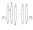
図1は、典型的なインターディジタルフィルタを示す。 FIG. 1 shows a typical interdigital filter.
図1を参照すると、一般的なインターディジタルフィルタは、マイクロ波帯域で使用される帯域通過フィルタ(band pass filter)の一種である。この帯域通過フィルタは、平面基板の形態を有し、入力線路(Input)と出力線路(Output)との間に複数の線路共振器110、120、130、140、及び150が配置される。線路共振器110、120、130、140、及び150は、同一の形態の複数の伝送線路によって実現される。線路共振器110、120、130、140、及び150は、それらの間の予め決定された間隔だけ離隔して配置される。図1では、第1の線路共振器110と第2の線路共振器120との間隔は、g12と表示され、設計帯域幅に応じて共振器間の間隔が決定される。線路共振器110、120、130、140、及び150は一方の側のみで接地され、接地される側は交互である。例えば、奇数番目の共振器110、130、及び150の第1の側(下側)が接地された場合、偶数番目の共振器120、及び140の第2の側(上側)が接地される。
Referring to FIG. 1, a general interdigital filter is a type of band pass filter used in a microwave band. This band pass filter has a form of a planar substrate, and a plurality of
インターディジタルフィルタの線路共振器110、120、130、140、及び150は、ユーザにより所望される帯域の中心周波数で90゜の電気的長さを有していなければならない。ここで、線路共振器110、120、130、140、及び150が中心周波数で90゜の電気的長さを有するということは、線路共振器110、120、130、140、及び150の各々がこの中心周波数でλ(波長)/4の長さを有することを意味する。例えば、1GHzにおいて1λは300mmである。従って、90゜の電気的長さを有するためには、1GHzにおいて線路共振器の長さは75mmでなければならない。周波数が高ければ高いほど波長は短くなるため、線路共振器の長さは短くなる。
The interdigital
要約すると、非常に高い周波数では波長は短いので、線路共振器は短くならざるを得ない。例えば、中心周波数が60GHzの場合、自由空間で90゜の電気的長さを有するためには、線路共振器の長さは1.25mmでなければならない。しかし、図1のインターディジタルフィルタを実際に設計するとき、即ち、線路共振器を所定の基板上に実現する場合、線路共振器の長さは、幅に比べてそれほど長くない。また、共振器の長さが短くなるとき、インターディジタルフィルタの挿入損失に影響する品質係数(Q)は低くなる。 In summary, at very high frequencies, the wavelength is short, so the line resonator must be short. For example, when the center frequency is 60 GHz, the length of the line resonator must be 1.25 mm in order to have an electrical length of 90 ° in free space. However, when the interdigital filter of FIG. 1 is actually designed, that is, when the line resonator is realized on a predetermined substrate, the length of the line resonator is not so long compared to the width. Further, when the length of the resonator is shortened, the quality factor (Q) that affects the insertion loss of the interdigital filter is lowered.
この問題は、高い周波数において90゜の電気的長さを有する線路共振器を使用する代わりに、270゜の電気的長さを有する線路共振器を使用することにより、解決することができる。しかし、270゜の電気的長さを有する線路共振器を用いて結合線路フィルタが形成される場合、ユーザにより所望されない低周波数帯域でも形成される通過帯域の問題がある。 This problem can be solved by using a line resonator having an electrical length of 270 ° instead of using a line resonator having an electrical length of 90 ° at a high frequency. However, when a coupled line filter is formed using a line resonator having an electrical length of 270 °, there is a problem of a pass band formed even in a low frequency band that is not desired by the user.
本発明の一実施形態は、広帯域特性及び低挿入損失を有する結合線路フィルタを提供することに向けられる。 One embodiment of the present invention is directed to providing a coupled line filter having broadband characteristics and low insertion loss.
本発明の別の実施形態は、ユーザによって所望される周波数帯域でのみ通過帯域を形成することができる結合線路フィルタを提供することに向けられる。 Another embodiment of the invention is directed to providing a coupled line filter that can form a pass band only in a frequency band desired by a user.
本発明の別の実施形態は、多層構造を有する基板に好適な結合線路フィルタを提供することに向けられる。 Another embodiment of the present invention is directed to providing a coupled line filter suitable for a substrate having a multilayer structure.
本発明の他の目的及び利点は、次の説明によって理解することができ、本発明の実施形態への参照と共に明らかになる。また、本発明が属する分野における当業者にとって、本発明の目的及び利点を特許請求の範囲に記載された手段及びその組み合わせによって達成できることは、明白である。 Other objects and advantages of the present invention can be understood by the following description, and become apparent with reference to the embodiments of the present invention. It will be apparent to those skilled in the art to which the present invention pertains that the objects and advantages of the present invention can be achieved by means of the means recited in the claims and combinations thereof.
本発明の一態様によると、予め決定された中心周波数で270゜の電気的長さを各々が有し、入力ポートと出力ポートとに接続され、互いに平行に配置されている、第1の線路共振器及び第2の線路共振器と、第1の線路共振器と第2の線路共振器との間に配置され、各々が中心周波数で90゜の電気的長さを有し、第1の側が第1の線路共振器及び第2の線路共振器の第1の側に整列される、1つ又は複数の線路共振器を備える第3の線路共振部とを備え、結合線路フィルタの次数は、第3の線路共振部内の線路共振器の個数と、第1の線路共振器及び第2の線路共振器とを合わせることによって決定されることを特徴とする、結合線路フィルタが提供される。 According to one aspect of the present invention, a first line, each having an electrical length of 270 ° at a predetermined center frequency, connected to an input port and an output port, and arranged parallel to each other The first and second line resonators are disposed between the resonator and the second line resonator, and each of the first line resonator and the second line resonator has an electrical length of 90 ° at the center frequency. A first line resonator and a third line resonator with one or more line resonators aligned with the first side of the first line resonator and the second line resonator, the order of the coupled line filter is A coupled line filter is provided, which is determined by combining the number of line resonators in the third line resonator unit with the first line resonator and the second line resonator.
本発明の別の態様によると、結合線路フィルタ内で線路共振器を配置する方法が提供される。この方法は、予め決定された中心周波数で270゜の電気的長さを共に有する第1の線路共振器と第2の線路共振器とを互いに平行に配置するステップと、中心周波数で90゜の電気的長さを有する1つ又は複数の線路共振器を備える第3の線路共振部を、第1の線路共振器と第2の線路共振器との間に配置するステップであって、第3の線路共振部の線路共振器の第1の側が第1の線路共振器及び第2の線路共振器の第1の側に整列されるように配置されるステップとを含むことを特徴とする。 In accordance with another aspect of the present invention, a method for placing a line resonator within a coupled line filter is provided. The method includes placing a first line resonator and a second line resonator having both electrical lengths of 270 ° at a predetermined center frequency in parallel with each other, and 90 ° at the center frequency. Disposing a third line resonator having one or more line resonators having an electrical length between the first line resonator and the second line resonator; And a step of arranging the first side of the line resonator of the line resonance unit to be aligned with the first side of the first line resonator and the second line resonator.
本発明に係る結合線路フィルタを使用すれば、多層構造の基板に好適であるため、集積化に有利であるという利点がある。また、広帯域特性を有し、かつ、挿入損失が低いという利点がある。更に、多層基板への実現が可能で、結合量を増加させることにより、使用周波数帯域を拡大できるという利点がある。なお、ユーザの所望する周波数帯域でのみ通過帯域を形成し、それ以外の低周波数帯域では通過帯域を形成しないという利点がある。 The use of the coupled line filter according to the present invention is advantageous for integration because it is suitable for a multilayer substrate. In addition, there are advantages of having wideband characteristics and low insertion loss. Further, it is possible to realize a multilayer substrate, and there is an advantage that the use frequency band can be expanded by increasing the coupling amount. Note that there is an advantage that a pass band is formed only in a frequency band desired by the user, and no pass band is formed in other low frequency bands.
本発明の利点、特徴、及び態様は、以下で説明される添付図面への参照と共に、次の説明から明らかになるであろう。以下で用いられる用語は、本発明の理解を容易にするためのものであって、様々な用語は、同じ用途で使用されるにもかかわらず、各製造会社又は研究グループによって、異なることがある。 Advantages, features, and aspects of the present invention will become apparent from the following description, together with reference to the accompanying drawings described below. The terms used below are for facilitating the understanding of the present invention, and various terms may be different for each manufacturing company or research group even though they are used in the same application. .
図2は、本発明の第1の実施形態に係る結合線路フィルタを示す。 FIG. 2 shows a coupled line filter according to the first embodiment of the present invention.
図2を参照すると、本発明の第1の実施形態に係る結合線路フィルタは、入力線路(Input)と、出力線路(Output)と、複数の線路共振器210、211、212、…、213、及び214とを備える。
Referring to FIG. 2, the coupled line filter according to the first embodiment of the present invention includes an input line (Input), an output line (Output), and a plurality of
入力線路は第1の線路共振器210に直接接続され、出力線路は最後の線路共振器214に直接接続される。線路共振器210、211、212、…、213、及び214の個数は、ユーザの所望する次数(order)に基づいて決定される。ユーザが3次の結合線路フィルタを設計することを希望する場合、結合線路フィルタは3つの線路共振器で実現される。
The input line is directly connected to the
また、線路共振器210、211、212、…、213、及び214の各々は、設計値に応じて決定された幅を有し、線路共振器210、211、212、…、213、及び214は、平行に配置される。しかし、線路共振器210、211、212、…、213、及び214の長さは、図2に示すように、互いに異なる。即ち、線路共振器210、211、212、…、213、及び214のうち、図2に示される、入力線路から奇数番目の場所に配置される線路共振器210、212、…、214は(以下、奇数番目に位置する線路共振器とする)、予め決定された第1の長さを有するのに対して、入力線路から偶数番目の場所に配置される線路共振器211、…、213は(以下、偶数番目に位置する線路共振器とする)、予め決定された第2の長さを有する。
In addition, each of the
本発明の第1の実施形態では、第1の長さと第2の長さが異なり、第1の長さが第2の長さより長いと仮定する。偶数番目に位置する線路共振器211、…、213の第2の長さは、奇数番目に位置する線路共振器210、212、…、214の第1の長さの1/3とすることが可能である。奇数番目に位置する線路共振器210、212、…、214の電気的長さを270゜にすることが可能である一方、偶数番目に位置する線路共振器211、…、213の電気的長さを90゜にすることが可能である。
In the first embodiment of the present invention, it is assumed that the first length is different from the second length, and the first length is longer than the second length. The second length of the even-numbered
また、複数の線路共振器210、211、212、…、213、及び214の各々は、接地される一方の側を有する。ここで、接地は、接地線路の形成により実現され(図示せず)、線路共振器210、211、212、…、213、及び214の各々に直接接続することができる。また、接地面(図示せず)を、線路共振器210、211、212、…、213、及び214が配置され、複数のビアを介して接地のために線路共振器210、211、212、…、213、及び214に接続された、所定基板の上又は下に配置することができる。このような接地面(図示せず)は、後で図10を参照して詳細に説明される。
In addition, each of the plurality of
複数の線路共振器210、211、212、…、213、及び214は、2つの側を有するが、一方の側のみが接地される。更に、線路共振器210、211、212、…、213、及び214は同一方向に接地される。
The plurality of
また、奇数番目に位置する線路共振器210、212、…、214の接地された側を、偶数番目に位置する線路共振器211、…、213の接地された側と、同様の位置に配列することができる。
Further, the grounded sides of the odd-numbered
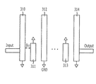
図3は、本発明の第2の実施形態に係る結合線路フィルタを示す。 FIG. 3 shows a coupled line filter according to a second embodiment of the present invention.
図3を参照すると、本発明の第2の実施形態に係る結合線路フィルタは、図2に示す第1の実施形態に係る結合線路フィルタに類似する構造を有する。この2つの結合線路フィルタ間の差異は、第2の実施形態に係る結合線路フィルタが線路共振器210、211、212、…、213、及び214の接地方向と異なる、線路共振器310、311、312、…、313、及び314の接地方向を有することである。即ち、複数の線路共振器310、311、312、…、313、及び314のうち、偶数番目に位置する線路共振器311、…、313は、他方の側を接地させる。ここで、偶数番目に位置する線路共振器311、…、313の他方の側とは、奇数番目に位置する線路共振器310、312、…、314が配置されない側を意味する。
Referring to FIG. 3, the coupled line filter according to the second embodiment of the present invention has a structure similar to the coupled line filter according to the first embodiment shown in FIG. The difference between the two coupled line filters is that the coupled line filter according to the second embodiment differs from the ground direction of the
図2及び図3に示す本発明の実施形態は、長さの短い共振器が、長さの長い共振器と同一の接地方向を有すること、又は長さの長い共振器と反対の接地方向を有することを示す。図2及び図3に示す結合線路フィルタは、同様の効果を有するが、図2に示す第1の実施形態に係る結合線路フィルタは、線路共振器が同一の接地方向を有するため、図3に示す第2の実施形態に係る結合線路フィルタより少ない結合量を有する。従って、図3に示す第2の実施形態の結合線路フィルタが、この2つの結合線路フィルタ間ではより効果的である。 The embodiment of the present invention shown in FIGS. 2 and 3 is such that the short-length resonator has the same grounding direction as the long-length resonator, or has a grounding direction opposite to that of the long-length resonator. It shows having. The coupled line filter shown in FIGS. 2 and 3 has the same effect, but the coupled line filter according to the first embodiment shown in FIG. 2 has the same grounding direction in the line resonator, so that FIG. It has less coupling than the coupled line filter according to the second embodiment shown. Therefore, the coupled line filter of the second embodiment shown in FIG. 3 is more effective between the two coupled line filters.
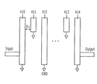
図4は、本発明の第3の実施形態に係る結合線路フィルタを示す。 FIG. 4 shows a coupled line filter according to a third embodiment of the present invention.
図4を参照すると、本発明の第3の実施形態に係る結合線路フィルタは、図2に示す第1の実施形態に係る結合線路フィルタに類似している。この2つの結合線路フィルタ間の差異は、図2に示す第1の実施形態に係る結合線路フィルタの偶数番目に位置する線路共振器211、…、213は、奇数番目に位置する線路共振器210、212、…、214の一方の側に配置されるのに対し、図4に示す第3の実施形態に係る結合線路フィルタの偶数番目に位置する線路共振器411、…、413は、奇数番目に位置する線路共振器410、412、…、414の他方の側に配置されることである。図4に示す第3の実施形態に係る結合線路フィルタの偶数番目に位置する線路共振器411、…、413は、偶数番目に位置する線路共振器411、…、413が配置されない、奇数番目に位置する線路共振器410、412、…、414の側に向かって同一方向で接地される。
Referring to FIG. 4, the coupled line filter according to the third embodiment of the present invention is similar to the coupled line filter according to the first embodiment shown in FIG. The difference between the two coupled line filters is that the even-numbered
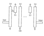
図5は、本発明の第4の実施形態に係る結合線路フィルタを示す。 FIG. 5 shows a coupled line filter according to a fourth embodiment of the present invention.
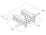
図5を参照すると、本発明の第4の実施形態の結合線路フィルタは、図3に示す本発明の第2の実施形態の結合線路フィルタに類似している。この2つの結合線路フィルタ間の差異は、図3に示す第2の実施形態の結合線路フィルタの偶数番目に位置する線路共振器311、…、313は、奇数番目に位置する線路共振器310、312、…、314の一方の側に配置されるのに対し、図5に示す第4の実施形態の結合線路フィルタの偶数番目に位置する線路共振器511、…、513は、奇数番目に位置する線路共振器510、512、…、514の他方の側に配置されることである。図5に示す第4の実施形態の結合線路フィルタの偶数番目に位置する線路共振器511、…、513は、偶数番目に位置する線路共振器511、…、513が配置される、奇数番目に位置する線路共振器510、512、…、514の側に向かって同一方向で接地される。
Referring to FIG. 5, the coupled line filter of the fourth embodiment of the present invention is similar to the coupled line filter of the second embodiment of the present invention shown in FIG. The difference between the two coupled line filters is that the
図4及び図5に示す本発明の実施形態は、長さの短い共振器が、長さの長い共振器と同一の接地方向を有すること、又は長さの長い共振器と反対の接地方向を有することを示す。図4及び図5に示す結合線路フィルタは、同様の効果を有するが、図4に示す第3の実施形態の結合線路フィルタは、同一の接地方向を有するので、図5に示す第4の実施形態の結合線路フィルタより少ない結合量を有する。従って、図5に示す第4の実施形態の結合線路フィルタが、この2つの結合線路フィルタ間ではより効果的である。 The embodiment of the present invention shown in FIGS. 4 and 5 is such that the short-length resonator has the same grounding direction as the long-length resonator, or has a grounding direction opposite to that of the long-length resonator. It shows having. The coupled line filter shown in FIGS. 4 and 5 has the same effect, but since the coupled line filter of the third embodiment shown in FIG. 4 has the same ground direction, the fourth implementation shown in FIG. The amount of coupling is smaller than that of the coupled line filter of the form. Therefore, the coupled line filter of the fourth embodiment shown in FIG. 5 is more effective between the two coupled line filters.
図6は、本発明の第5の実施形態に係る結合線路フィルタを示す。 FIG. 6 shows a coupled line filter according to a fifth embodiment of the present invention.
図6を参照すると、本発明の第5の実施形態の結合線路フィルタは、図5に示す第4の実施形態の結合線路フィルタの偶数番目に位置する線路共振器511、…、513に、図3に示す第2の実施形態の結合線路フィルタの構造を追加した構造を有する。
Referring to FIG. 6, the coupled line filter of the fifth embodiment of the present invention is shown in the
第5の実施形態の結合線路フィルタでは、偶数番目に位置する線路共振器611、612、…、614、615は、90゜の電気的長さを有し、第1の線路共振器610と最後の線路共振器616の両側に配置されるので、第2の線路共振器611と612との間の間隔はλ/4となる。
In the coupled line filter of the fifth embodiment, the even-numbered
図7は、本発明の第6の実施形態に係る結合線路フィルタを示す。 FIG. 7 shows a coupled line filter according to a sixth embodiment of the present invention.
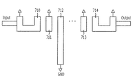
図7を参照すると、本発明の第6の実施形態の結合線路フィルタは、線路共振器510、511、512、…、513、及び514のうち、第1の線路共振器510と最後の線路共振器514の形態を除いて、図5に示す本発明の第4の実施形態の結合線路フィルタの構造を有する。他の線路共振器511、512、…、513は同一である。
Referring to FIG. 7, the coupled line filter according to the sixth exemplary embodiment of the present invention includes the
第1の線路共振器710及び最後の線路共振器714は、「U」状に湾曲した形態を有する。第1の線路共振器710及び最後の線路共振器714は「U」状に曲げられるが、それらは270゜の電気的長さを維持する。
The
図8は、本発明の第7の実施形態に係る結合線路フィルタを示す。 FIG. 8 shows a coupled line filter according to a seventh embodiment of the present invention.
図8を参照すると、本発明の第7の実施形態の結合線路フィルタは、本発明の第6の実施形態の結合線路フィルタに類似している。この2つの結合線路フィルタの差異は、第1の線路共振器810と最後の線路共振器814を除くすべての線路共振器811、812、…、813が90゜の電気的長さを有することである。
Referring to FIG. 8, the coupled line filter of the seventh embodiment of the present invention is similar to the coupled line filter of the sixth embodiment of the present invention. The difference between the two coupled line filters is that all
上述のように、図2乃至図8に示す本発明の実施形態に係る結合線路フィルタは、従来のインターディジタルフィルタで使用される伝送線路より少ない伝送線路を用いて共振器を形成するので、経済的である。更に、多層構造の基板を使用するので、他の回路と容易に集積可能であるという点で有利である。 As described above, the coupled line filter according to the embodiment of the present invention shown in FIGS. 2 to 8 forms a resonator using fewer transmission lines than the transmission lines used in the conventional interdigital filter. Is. Furthermore, since a multilayer substrate is used, it is advantageous in that it can be easily integrated with other circuits.
また、図2乃至図8に示す本発明の実施形態に係る結合線路フィルタは、ユーザの所望する高周波数帯域以外の低周波帯域で通過帯域を作らないという別の利点がある。更に、広帯域特性も低挿入速度も有する。以下では、これらの有利な態様について添付図面を参照して説明する。 Further, the coupled line filter according to the embodiment of the present invention shown in FIGS. 2 to 8 has another advantage that a pass band is not formed in a low frequency band other than a high frequency band desired by a user. In addition, it has wideband characteristics and low insertion speed. These advantageous aspects are described below with reference to the accompanying drawings.
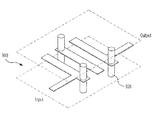
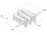
図9は、LTCC技術を適用した図1の典型的な3次インターディジタルフィルタを示す斜視図である。図10は、3段に積層された図1の典型的な3次インターディジタルフィルタを示す斜視図である。図11は、LTCC技術を適用することにより3段に積層された図3に示す本発明の第2の実施形態の結合線路フィルタを示す斜視図である。 FIG. 9 is a perspective view showing the typical third-order interdigital filter of FIG. 1 to which the LTCC technique is applied. FIG. 10 is a perspective view showing the typical third-order interdigital filter of FIG. 1 stacked in three stages. FIG. 11 is a perspective view showing the coupled line filter of the second embodiment of the present invention shown in FIG. 3 stacked in three stages by applying LTCC technology.
図9を参照すると、典型的な3次インターディジタルフィルタを構成する入力線路、出力線路、及び複数の線路共振器が、LTCC基板910内に配置される。ここで、LTCC基板910の上面と下面には接地面が設けられる。LTCC基板910内の線路共振器の各々は、ビア920を介して接地基板に接続される一方の側を有する。
Referring to FIG. 9, an input line, an output line, and a plurality of line resonators constituting a typical third-order interdigital filter are disposed in the
一方、実際に実現されたLTCC基板910は、5.9の誘電率と、0.02の損失正接を有し、線路共振器は、電気的長さが270゜である伝送線路から形成された。
Meanwhile, the actually realized
図10は、3段に積層された図1の典型的な3次インターディジタルフィルタを示す。図9に示すインターディジタルフィルタのように、LTCC基板1010の上面と下面には接地面が設けられており、ビア1020を介して複数の線路共振器が接地面に接続される。線路共振器は、図9に示す複数の線路共振器と同様に、電気的長さが270゜の伝送線路を用いて実現される。
FIG. 10 shows the typical third-order interdigital filter of FIG. 1 stacked in three stages. As in the interdigital filter shown in FIG. 9, ground planes are provided on the upper and lower surfaces of the
図11を参照すると、3段で積層されLTCC基板1110内に配置された、図3に示す本発明の第2の実施形態の結合線路フィルタを示している。この構造においても、ビア1120を介して複数の共振器が接地面に接続されている。図11に示す線路共振器のうち、長さの長い共振器は、中心周波数で電気的長さが270゜の伝送線路から形成され、長さの短い共振器は、電気的長さが、長さの長い共振器の1/3、即ち、90゜の伝送線路から形成される。
Referring to FIG. 11, there is shown a coupled line filter according to the second embodiment of the present invention shown in FIG. 3, which is stacked in three stages and arranged in an
このような図9乃至図11に示す結合線路フィルタの効果は、高周波回路の解析において高い信頼性を有する電磁界解析を利用して分析された。以下、図12及び図13を参照して、図9乃至図11に示すフィルタの効果を説明する。 The effects of the coupled line filter shown in FIGS. 9 to 11 were analyzed using electromagnetic field analysis having high reliability in the analysis of a high frequency circuit. The effects of the filters shown in FIGS. 9 to 11 will be described below with reference to FIGS.
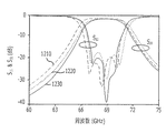
図12は、図9乃至図11に示す結合線路フィルタの反射係数S11と透過係数S21とを比較的に示すグラフである。 Figure 12 is a graph showing the reflection coefficient S 11 of the coupled line filter shown in FIGS. 9 to 11 and transmission coefficient S 21 relatively.
このグラフでは、参照番号1210は、図9に示す結合線路フィルタの反射係数S11と透過係数S21とを示すグラフであり、参照番号1220は、図10に示す結合線路フィルタの反射係数S11と透過係数S21とを示すグラフである。参照番号1230は、図11に示す結合線路フィルタの反射係数S11と透過係数S21とを示すグラフである。
In this graph,
図12のグラフから、図9及び図10に示す一般的なインターディジタルフィルタが類似する反射係数S11と透過係数S21とを有することがわかる。図示していないが、図10の結合線路フィルタの線路共振器間の間隔を約40μmより広くする場合、図10の結合線路フィルタの線路共振器間は、図9の結合線路フィルタと類似する結果を依然として有する。 From the graph of FIG. 12, it can be seen that the general interdigital filters shown in FIGS. 9 and 10 have similar reflection coefficients S 11 and transmission coefficients S 21 . Although not shown, when the interval between the line resonators of the coupled line filter of FIG. 10 is made larger than about 40 μm, the result between the line resonators of the coupled line filter of FIG. 10 is similar to that of the coupled line filter of FIG. Still have.
図12を再び参照すると、図11に示す本発明の結合線路フィルタは、図9及び図10に示す一般的なインターディジタルフィルタと類似の周波数特性を有することが観察される。 Referring again to FIG. 12, it can be observed that the coupled line filter of the present invention shown in FIG. 11 has a frequency characteristic similar to that of the general interdigital filter shown in FIGS.
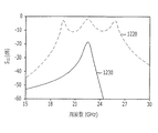
図13は、図10乃至図11の結合線路フィルタの透過係数S21を低周波数で比較的に示すグラフである。この図において、参照番号1220は、図10に示す結合線路フィルタの透過係数S21を示すグラフであり、参照番号1230は、図11に示す結合線路フィルタの透過係数S21を示すグラフである。
FIG. 13 is a graph relatively showing the transmission coefficient S 21 of the coupled line filter of FIGS. 10 to 11 at a low frequency. In this figure,
図13を参照すると、図11に示す本発明の結合線路フィルタは、低い周波数帯域で図10に示す一般的なインターディジタルフィルタより約20dB超の信号を遮断する効果を有することが観察される。このような結果に基づいて、図11に示す本発明の結合線路フィルタにより多くの短い線路共振器を使用すると、低周波数帯域における信号遮断の効果が増加されることが予想される。 Referring to FIG. 13, it can be observed that the coupled line filter of the present invention shown in FIG. 11 has an effect of blocking a signal exceeding about 20 dB from the general interdigital filter shown in FIG. 10 in a low frequency band. Based on such a result, it is expected that the signal blocking effect in the low frequency band is increased when many short line resonators are used in the coupled line filter of the present invention shown in FIG.
具体的な実施形態に関して本発明が説明されてきたが、特許請求の範囲で定義される本発明の趣旨及び範囲から逸脱しないで、様々な変化及び変更をなすことができることは、当業者にとって明白であろう。 While the invention has been described in terms of specific embodiments, it will be apparent to those skilled in the art that various changes and modifications can be made without departing from the spirit and scope of the invention as defined in the claims. Will.
Claims (20)
前記第1の線路共振器と前記第2の線路共振器との間に配置され、第1の側が前記第1の線路共振器及び前記第2の線路共振器の第1の側に整列され、各々が前記中心周波数で90゜の電気的長さを有する1つ又は複数の線路共振器を備える第3の線路共振部と
を備える結合線路フィルタであって、
前記結合線路フィルタの次数は、前記第3の線路共振部内に含まれる線路共振器の個数を、前記第1の線路共振器及び前記第2の線路共振器と合わせることにより決定されることを特徴とする結合線路フィルタ。 A first line resonator and a second line resonator, each having an electrical length of 270 ° at a predetermined center frequency, connected to the input port and the output port, and arranged parallel to each other; ,
Disposed between the first line resonator and the second line resonator, the first side being aligned with the first side of the first line resonator and the second line resonator; A coupled line filter comprising: a third line resonating unit comprising one or more line resonators each having an electrical length of 90 ° at the center frequency;
The order of the coupled line filter is determined by combining the number of line resonators included in the third line resonator unit with the first line resonator and the second line resonator. A coupled line filter.
前記第1の線路共振器を基準として、奇数番目の場所に配置される線路共振器は、前記中心周波数で90゜の電気的長さを有する一方、偶数番目の場所に配置される線路共振器は、前記中心周波数で270゜の電気的長さを有することを特徴とする結合線路フィルタ。 The coupled line filter according to claim 1, wherein the number of line resonators included in the third line resonance unit is 2n + 1 (where n is a natural number),
The line resonators disposed at odd-numbered locations with respect to the first line resonator have an electrical length of 90 ° at the center frequency, while the line resonators disposed at even-numbered locations. Has an electrical length of 270 ° at the center frequency.
前記偶数番目の場所の線路共振器の第1の側は、前記接地に結合される一方、前記奇数番目の場所の線路共振器の第1の側又は第2の側は、前記接地に結合されることを特徴とする結合線路フィルタ。 5. The coupled line filter of claim 4, wherein the first side of the first line resonator and the second line resonator are coupled to ground,
The first side of the line resonator at the even-numbered location is coupled to the ground, while the first side or the second side of the line resonator at the odd-numbered location is coupled to the ground. A coupled line filter.
前記偶数番目に位置する線路共振器の前記第2の側は、前記接地に結合される一方、前記奇数番目に位置する線路共振器の第1の側又は第2の側は、前記接地に結合されることを特徴とする結合線路フィルタ。 5. The coupled line filter of claim 4, wherein a second side of the first line resonator and the second line resonator is coupled to ground,
The second side of the even-numbered line resonator is coupled to the ground, while the first or second side of the odd-numbered line resonator is coupled to the ground. A coupled line filter, wherein:
前記第1の線路共振器を基準として、奇数番目の位置に配置される線路共振器は、前記中心周波数で90゜の電気的長さを有する一方、偶数番目の位置に配置される線路共振器は、前記中心周波数で270゜の電気的長さを有することを特徴とする結合線路フィルタ。 The coupled line filter according to claim 8, wherein the number of line resonators included in the third line resonance unit is 2n + 1 (where n is a natural number),
The line resonators arranged at odd-numbered positions with respect to the first line resonator have an electrical length of 90 ° at the center frequency, while the line resonators arranged at even-numbered positions. Has an electrical length of 270 ° at the center frequency.
前記第1の線路共振器を基準として、奇数番目の場所に配置される線路共振器は、前記中心周波数で90°の電気的長さを有する一方、偶数番目の場所に配置される線路共振器は、前記中心周波数で90°の電気的長さを有することを特徴とする結合線路フィルタ。 The coupled line filter according to claim 8, wherein the number of line resonators included in the third line resonance unit is 2n + 1 (where n is a natural number),
The line resonators arranged at odd-numbered locations with respect to the first line resonator have an electrical length of 90 ° at the center frequency, while the line resonators arranged at even-numbered locations Has a 90 ° electrical length at the center frequency.
前記複数の第1の線路共振器、前記複数の第2の線路共振器、及び前記複数の第3の線路共振部はそれぞれ、積層構造から成ることを特徴とする結合線路フィルタ。 The coupled line filter according to claim 1, comprising a plurality of the first line resonator, the second line resonator, and the third line resonator.
Each of the plurality of first line resonators, the plurality of second line resonators, and the plurality of third line resonators has a laminated structure, and is a coupled line filter.
前記中心周波数で90゜の電気的長さを有する1つ又は複数の線路共振器を備える第3の線路共振部を、前記第1の線路共振器と前記第2の線路共振器との間に配置するステップと
を備える、結合線路フィルタ内の線路共振器を配置する方法であって、
前記第3の線路共振部の前記線路共振器の第1の側は、前記第1の線路共振器及び前記第2の線路共振器の第1の側に整列されることを特徴とする結合線路フィルタ内の線路共振器を配置する方法。 Placing a first line resonator and a second line resonator having both electrical lengths of 270 ° at a predetermined center frequency in parallel with each other;
A third line resonator comprising one or more line resonators having an electrical length of 90 ° at the center frequency, between the first line resonator and the second line resonator; A step of arranging a line resonator in a coupled line filter, comprising the steps of:
A coupled line characterized in that a first side of the line resonator of the third line resonator is aligned with a first side of the first line resonator and the second line resonator. A method of arranging a line resonator in a filter.
前記第1の線路共振器及び前記第2の線路共振器の前記第1の側を接地に接続するステップと、前記第3の線路共振部の前記線路共振器の前記第1の側又は第2の側を前記接地に接続するステップとを更に備えることを特徴とする方法。 The method of claim 13, wherein
Connecting the first side of the first line resonator and the second line resonator to ground, and the first side or the second side of the line resonator of the third line resonator. And further comprising the step of connecting said side to said ground.
前記第1の線路共振器及び前記第2の線路共振器の第2の側を接地に接続するステップと、前記第3の線路共振部の前記線路共振器の前記第1の側又は第2の側を前記接地に接続するステップとを更に備えることを特徴とする方法。 The method of claim 13, wherein
Connecting a second side of the first line resonator and the second line resonator to ground, and the first side or the second side of the line resonator of the third line resonator. Connecting a side to the ground.
前記第1の線路共振器を基準として奇数番目の場所に配置される線路共振器は、前記中心周波数で90゜の電気的長さを有する一方、偶数番目の場所に配置される線路共振器は、前記中心周波数で270゜の電気的長さを有することを特徴とする方法。 The method according to claim 13, wherein the number of the line resonators included in the third line resonance unit is 2n + 1 (where n is a natural number),
Line resonators arranged at odd-numbered locations with respect to the first line resonator have an electrical length of 90 ° at the center frequency, while line resonators arranged at even-numbered locations are And having an electrical length of 270 ° at the center frequency.
前記中心周波数で90゜の電気的長さを有する線路共振器を配置するステップであって、前記第1の線路共振器及び前記第2の線路共振器の第2の側に整列され、且つ前記偶数番目に位置する線路共振器と一列に配列されるステップを更に備えることを特徴とする方法。 The method of claim 16, wherein
Disposing a line resonator having an electrical length of 90 ° at the center frequency, wherein the line resonator is aligned with a second side of the first line resonator and the second line resonator; and The method further comprising the step of being aligned with the even-numbered line resonators.
前記第1の線路共振器を基準として、奇数番目の場所に配置される線路共振器は、前記中心周波数で90゜の電気的長さを有する一方、偶数番目の場所に配置される線路共振器は、前記中心周波数で270゜の電気的長さを有することを特徴とする方法。 The method according to claim 18, wherein the number of the line resonators included in the third line resonance unit is 2n + 1 (where n is a natural number),
The line resonators disposed at odd-numbered locations with respect to the first line resonator have an electrical length of 90 ° at the center frequency, while the line resonators disposed at even-numbered locations. Has an electrical length of 270 ° at the center frequency.
前記第1の線路共振器を基準として、奇数番目の場所に配置される線路共振器は、前記中心周波数で90°の電気的長さを有する一方、偶数番目の場所に配置される線路共振器は、前記中心周波数で90°の電気的長さを有することを特徴とする方法。 The method according to claim 18, wherein the number of the line resonators included in the third line resonance unit is 2n + 1 (where n is a natural number),
The line resonators arranged at odd-numbered locations with respect to the first line resonator have an electrical length of 90 ° at the center frequency, while the line resonators arranged at even-numbered locations Has an electrical length of 90 ° at the center frequency.
Applications Claiming Priority (2)
| Application Number | Priority Date | Filing Date | Title |
|---|---|---|---|
| KR20080124650 | 2008-12-09 | ||
| KR1020090022531A KR101160560B1 (en) | 2008-12-09 | 2009-03-17 | Coupled line filter and method for placing thereof |
Publications (1)
| Publication Number | Publication Date |
|---|---|
| JP2010141877A true JP2010141877A (en) | 2010-06-24 |
Family
ID=42230402
Family Applications (1)
| Application Number | Title | Priority Date | Filing Date |
|---|---|---|---|
| JP2009247990A Pending JP2010141877A (en) | 2008-12-09 | 2009-10-28 | Coupled line filter, and arraying method therein |
Country Status (2)
| Country | Link |
|---|---|
| US (1) | US8314667B2 (en) |
| JP (1) | JP2010141877A (en) |
Cited By (4)
| Publication number | Priority date | Publication date | Assignee | Title |
|---|---|---|---|---|
| US8942774B2 (en) | 2011-09-29 | 2015-01-27 | Kabushiki Kaisha Toshiba | Radio-frequency filter comprising an even mode resonance of a same phase inside the bandwidth and an odd mode resonance of a reverse phase outside the bandwidth |
| JP2015171027A (en) * | 2014-03-07 | 2015-09-28 | 日立金属株式会社 | Filter, multicoupler using the same and antenna |
| JP2021136601A (en) * | 2020-02-27 | 2021-09-13 | 株式会社フジクラ | Directional coupler and attenuator |
| JPWO2022209278A1 (en) * | 2021-03-29 | 2022-10-06 |
Families Citing this family (18)
| Publication number | Priority date | Publication date | Assignee | Title |
|---|---|---|---|---|
| US8823470B2 (en) | 2010-05-17 | 2014-09-02 | Cts Corporation | Dielectric waveguide filter with structure and method for adjusting bandwidth |
| EP2515372A1 (en) * | 2011-04-20 | 2012-10-24 | Microelectronics Technology Inc. | Band-pass filter |
| US9130255B2 (en) | 2011-05-09 | 2015-09-08 | Cts Corporation | Dielectric waveguide filter with direct coupling and alternative cross-coupling |
| US9030278B2 (en) | 2011-05-09 | 2015-05-12 | Cts Corporation | Tuned dielectric waveguide filter and method of tuning the same |
| US9030279B2 (en) | 2011-05-09 | 2015-05-12 | Cts Corporation | Dielectric waveguide filter with direct coupling and alternative cross-coupling |
| US9130256B2 (en) | 2011-05-09 | 2015-09-08 | Cts Corporation | Dielectric waveguide filter with direct coupling and alternative cross-coupling |
| US9130258B2 (en) | 2013-09-23 | 2015-09-08 | Cts Corporation | Dielectric waveguide filter with direct coupling and alternative cross-coupling |
| US10050321B2 (en) | 2011-12-03 | 2018-08-14 | Cts Corporation | Dielectric waveguide filter with direct coupling and alternative cross-coupling |
| US10116028B2 (en) | 2011-12-03 | 2018-10-30 | Cts Corporation | RF dielectric waveguide duplexer filter module |
| US9666921B2 (en) | 2011-12-03 | 2017-05-30 | Cts Corporation | Dielectric waveguide filter with cross-coupling RF signal transmission structure |
| US9583805B2 (en) | 2011-12-03 | 2017-02-28 | Cts Corporation | RF filter assembly with mounting pins |
| WO2015157510A1 (en) | 2014-04-10 | 2015-10-15 | Cts Corporation | Rf duplexer filter module with waveguide filter assembly |
| FR3029368B1 (en) * | 2014-11-27 | 2018-04-06 | Time Reversal Communications | FILTERING DEVICE AND FILTERING ASSEMBLY WITH STRUCTURE OF ELECTRICALLY CONDUCTIVE BANDS |
| US11081769B2 (en) | 2015-04-09 | 2021-08-03 | Cts Corporation | RF dielectric waveguide duplexer filter module |
| US10483608B2 (en) | 2015-04-09 | 2019-11-19 | Cts Corporation | RF dielectric waveguide duplexer filter module |
| WO2020066621A1 (en) * | 2018-09-28 | 2020-04-02 | 株式会社村田製作所 | Bandpass filter, communication device, and resonator |
| US11437691B2 (en) | 2019-06-26 | 2022-09-06 | Cts Corporation | Dielectric waveguide filter with trap resonator |
| US12119549B2 (en) * | 2022-06-03 | 2024-10-15 | Apple Inc. | Electronic device antennas in acoustic cavities |
Citations (6)
| Publication number | Priority date | Publication date | Assignee | Title |
|---|---|---|---|---|
| JPS5885601A (en) * | 1981-11-17 | 1983-05-23 | Nec Corp | Microstrip type band-pass filter |
| JPS61274502A (en) * | 1985-05-08 | 1986-12-04 | アレン テレコム グループ,インコーポレイテッド | Interdigital type transmission-reception switch with notch resonator |
| JPH029203A (en) * | 1988-06-28 | 1990-01-12 | Sharp Corp | Microwave filter |
| JPH11186812A (en) * | 1997-12-22 | 1999-07-09 | Mitsubishi Electric Corp | High frequency filters and duplexers |
| JP2000059113A (en) * | 1998-08-04 | 2000-02-25 | Murata Mfg Co Ltd | Transmission line and transmission line resonator |
| JP2002084101A (en) * | 2000-09-06 | 2002-03-22 | Murata Mfg Co Ltd | Filter, multiplexer, and communicating device |
Family Cites Families (11)
| Publication number | Priority date | Publication date | Assignee | Title |
|---|---|---|---|---|
| JPS62260401A (en) * | 1986-05-02 | 1987-11-12 | Murata Mfg Co Ltd | Strip line filter |
| US5621366A (en) * | 1994-08-15 | 1997-04-15 | Motorola, Inc. | High-Q multi-layer ceramic RF transmission line resonator |
| KR100263704B1 (en) | 1998-01-17 | 2000-08-01 | 구자홍 | High frequency filter for high supper conductive microstrip line |
| JP3528044B2 (en) * | 1999-04-06 | 2004-05-17 | 株式会社村田製作所 | Dielectric filter, dielectric duplexer and communication device |
| US6927653B2 (en) * | 2000-11-29 | 2005-08-09 | Kyocera Corporation | Dielectric waveguide type filter and branching filter |
| KR20040050100A (en) | 2002-12-09 | 2004-06-16 | 엘지이노텍 주식회사 | Structure of two stage inter digital band pass filter |
| JP3860559B2 (en) * | 2003-05-20 | 2006-12-20 | 株式会社東芝 | Band pass filter |
| KR100605425B1 (en) * | 2004-10-18 | 2006-07-28 | 한국전자통신연구원 | Microstrip Bandpass Filters |
| JP4236663B2 (en) * | 2005-07-28 | 2009-03-11 | Tdk株式会社 | Electronic devices and filters |
| JP4171015B2 (en) * | 2005-09-29 | 2008-10-22 | 株式会社東芝 | Filter and wireless communication apparatus using the same |
| KR100651627B1 (en) * | 2005-11-25 | 2006-12-01 | 한국전자통신연구원 | Dielectric waveguide filter with cross coupling |
-
2009
- 2009-10-28 JP JP2009247990A patent/JP2010141877A/en active Pending
- 2009-10-28 US US12/607,884 patent/US8314667B2/en not_active Expired - Fee Related
Patent Citations (6)
| Publication number | Priority date | Publication date | Assignee | Title |
|---|---|---|---|---|
| JPS5885601A (en) * | 1981-11-17 | 1983-05-23 | Nec Corp | Microstrip type band-pass filter |
| JPS61274502A (en) * | 1985-05-08 | 1986-12-04 | アレン テレコム グループ,インコーポレイテッド | Interdigital type transmission-reception switch with notch resonator |
| JPH029203A (en) * | 1988-06-28 | 1990-01-12 | Sharp Corp | Microwave filter |
| JPH11186812A (en) * | 1997-12-22 | 1999-07-09 | Mitsubishi Electric Corp | High frequency filters and duplexers |
| JP2000059113A (en) * | 1998-08-04 | 2000-02-25 | Murata Mfg Co Ltd | Transmission line and transmission line resonator |
| JP2002084101A (en) * | 2000-09-06 | 2002-03-22 | Murata Mfg Co Ltd | Filter, multiplexer, and communicating device |
Cited By (7)
| Publication number | Priority date | Publication date | Assignee | Title |
|---|---|---|---|---|
| US8942774B2 (en) | 2011-09-29 | 2015-01-27 | Kabushiki Kaisha Toshiba | Radio-frequency filter comprising an even mode resonance of a same phase inside the bandwidth and an odd mode resonance of a reverse phase outside the bandwidth |
| JP2015171027A (en) * | 2014-03-07 | 2015-09-28 | 日立金属株式会社 | Filter, multicoupler using the same and antenna |
| JP2021136601A (en) * | 2020-02-27 | 2021-09-13 | 株式会社フジクラ | Directional coupler and attenuator |
| JPWO2022209278A1 (en) * | 2021-03-29 | 2022-10-06 | ||
| WO2022209278A1 (en) * | 2021-03-29 | 2022-10-06 | 株式会社村田製作所 | Dielectric filter |
| JP7559936B2 (en) | 2021-03-29 | 2024-10-02 | 株式会社村田製作所 | Dielectric Filter |
| US12506239B2 (en) | 2021-03-29 | 2025-12-23 | Murata Manufacturing Co., Ltd. | Dielectric filter |
Also Published As
| Publication number | Publication date |
|---|---|
| US8314667B2 (en) | 2012-11-20 |
| US20100141356A1 (en) | 2010-06-10 |
Similar Documents
| Publication | Publication Date | Title |
|---|---|---|
| JP2010141877A (en) | Coupled line filter, and arraying method therein | |
| Snyder et al. | Present and future trends in filters and multiplexers | |
| Jachowski | Passive enhancement of resonator Q in microwave notch filters | |
| US8130063B2 (en) | Waveguide filter | |
| JPWO2009133713A1 (en) | High frequency filter device | |
| US8970327B2 (en) | Filter based on a combined via structure | |
| US8330551B2 (en) | Dual band high frequency amplifier using composite right/left handed transmission line | |
| US20090027141A1 (en) | Filter circuit, filter circuit device, multilayered circuit board, and circuit module each including the filter circuit | |
| US7113060B2 (en) | Dielectric waveguide filter with inductive windows and coplanar line coupling | |
| US7468643B2 (en) | Bandpass filter and wireless communications equipment using same | |
| US7795996B2 (en) | Multilayered coplanar waveguide filter unit and method of manufacturing the same | |
| JP4598024B2 (en) | Band stop filter | |
| EP2865046A1 (en) | Bandpass filter and method of fabricating the same | |
| JP4550915B2 (en) | FILTER CIRCUIT, FILTER CIRCUIT ELEMENT, MULTILAYER CIRCUIT BOARD AND CIRCUIT MODULE HAVING THE SAME | |
| CN111095671B (en) | Dielectric filter and array antenna device | |
| JP2000357903A (en) | Flat filter | |
| US7408424B2 (en) | Compact RF circuit with high common mode attenuation | |
| KR101160560B1 (en) | Coupled line filter and method for placing thereof | |
| JP4251974B2 (en) | High frequency filter | |
| CN110492209B (en) | A self-packaged ultra-wideband balanced filter based on multilayer LCP circuit technology | |
| JP5417450B2 (en) | High frequency filter | |
| CN2938443Y (en) | Integrated waveguide cavity filter | |
| RU2259619C2 (en) | Bandpass filter | |
| JP6080538B2 (en) | Filter circuit | |
| JP3948281B2 (en) | Bandpass filter |
Legal Events
| Date | Code | Title | Description |
|---|---|---|---|
| RD02 | Notification of acceptance of power of attorney |
Free format text: JAPANESE INTERMEDIATE CODE: A7422 Effective date: 20121004 |
|
| RD04 | Notification of resignation of power of attorney |
Free format text: JAPANESE INTERMEDIATE CODE: A7424 Effective date: 20121004 |
|
| A621 | Written request for application examination |
Free format text: JAPANESE INTERMEDIATE CODE: A621 Effective date: 20121029 |
|
| A977 | Report on retrieval |
Free format text: JAPANESE INTERMEDIATE CODE: A971007 Effective date: 20130828 |
|
| A131 | Notification of reasons for refusal |
Free format text: JAPANESE INTERMEDIATE CODE: A131 Effective date: 20130903 |
|
| A601 | Written request for extension of time |
Free format text: JAPANESE INTERMEDIATE CODE: A601 Effective date: 20131203 |
|
| A602 | Written permission of extension of time |
Free format text: JAPANESE INTERMEDIATE CODE: A602 Effective date: 20131206 |
|
| A601 | Written request for extension of time |
Free format text: JAPANESE INTERMEDIATE CODE: A601 Effective date: 20140106 |
|
| A602 | Written permission of extension of time |
Free format text: JAPANESE INTERMEDIATE CODE: A602 Effective date: 20140109 |
|
| A521 | Written amendment |
Free format text: JAPANESE INTERMEDIATE CODE: A523 Effective date: 20140131 |
|
| A02 | Decision of refusal |
Free format text: JAPANESE INTERMEDIATE CODE: A02 Effective date: 20140617 |