JP2010124302A - Multichannel receiver - Google Patents
Multichannel receiver Download PDFInfo
- Publication number
- JP2010124302A JP2010124302A JP2008296772A JP2008296772A JP2010124302A JP 2010124302 A JP2010124302 A JP 2010124302A JP 2008296772 A JP2008296772 A JP 2008296772A JP 2008296772 A JP2008296772 A JP 2008296772A JP 2010124302 A JP2010124302 A JP 2010124302A
- Authority
- JP
- Japan
- Prior art keywords
- band
- signals
- frequency
- unit
- bands
- Prior art date
- Legal status (The legal status is an assumption and is not a legal conclusion. Google has not performed a legal analysis and makes no representation as to the accuracy of the status listed.)
- Pending
Links
Images


Abstract
Description
本発明は、多数の帯域の信号により構成される受信信号の中から所望の複数の帯域の信号のみを同時に復調するマルチチャネル受信装置に関するものである。 The present invention relates to a multi-channel receiving apparatus that simultaneously demodulates only signals of a plurality of desired bands from among received signals composed of signals of a large number of bands.
一般的な単一のチャネル受信装置は、多数の帯域の信号により構成される受信信号の中から所望の1つの帯域の信号のみをアナログ部で取り出し、その出力をA/D変換部に入力し、デジタル化された信号を復調部に入力して所望のデータを再生する。従来、複数の帯域の信号を受信するマルチチャネル受信装置においては、このアナログ部、A/D変換部、復調部を複数備えることによって実現していることが多い。しかし、このようにアナログ部、A/D変換部、復調部を複数備える構成では、回路規模が増大し、コストが大きくなってしまうことが問題である。 A general single channel receiving apparatus takes out only a signal of one desired band from a received signal composed of signals of a large number of bands in an analog section, and inputs the output to an A / D conversion section. Then, the digitized signal is input to the demodulator to reproduce desired data. Conventionally, multi-channel receivers that receive signals in a plurality of bands are often realized by including a plurality of analog units, A / D conversion units, and demodulation units. However, in such a configuration including a plurality of analog units, A / D conversion units, and demodulation units, there is a problem that the circuit scale increases and the cost increases.
この問題に対し、高速のクロック信号に対応したA/D変換部を備えることにより、受信信号を全帯域にわたって、デジタル化を行い、復調部にて各々の帯域の信号を分離することによって所望の複数の帯域の信号を受信する方法が提案されている(例えば、特許文献1参照。)。これにより、A/D変換部を1つ備えるだけで、さらにはアナログ部も簡素化して、複数帯域の信号の受信を可能としている。 In order to solve this problem, by providing an A / D converter corresponding to a high-speed clock signal, the received signal is digitized over the entire band, and a signal in each band is separated by a demodulator. A method for receiving signals in a plurality of bands has been proposed (see, for example, Patent Document 1). As a result, only one A / D conversion unit is provided, and the analog unit is further simplified to enable reception of signals in a plurality of bands.
しかしながら、例えば、地上デジタル放送など、全帯域が300MHzにもわたる信号をA/D変換するためには、600MHzという高速なクロック信号でA/D変換部を動作させなければならない。このような高速のクロック信号に対応したA/D変換部を、一定の性能を保ちつつ実現することは大変高度な技術が必要となり、そのコストは大きくなってしまう。また、そのような高速のクロック信号を、ジッタなどを抑えて、安定的にA/D変換部に供給することも大変困難であるという新たな問題を生じてしまう。 However, for example, in order to A / D convert a signal whose entire band extends over 300 MHz, such as terrestrial digital broadcasting, the A / D converter must be operated with a high-speed clock signal of 600 MHz. Realizing such an A / D conversion unit corresponding to a high-speed clock signal while maintaining a certain level of performance requires a very advanced technology, which increases the cost. In addition, there is a new problem that it is very difficult to stably supply such a high-speed clock signal to the A / D converter while suppressing jitter and the like.
本発明は上述の問題を解決するためになされたものであり、複数の帯域の信号を受信するマルチチャネル受信装置において、複数のA/D変換部を備えることによる回路規模の増大と、A/D変換部へ供給されるクロック信号の高速化を抑えることを目的とする。 The present invention has been made to solve the above-described problems. In a multi-channel receiving apparatus that receives signals of a plurality of bands, an increase in circuit scale by including a plurality of A / D conversion units, and A / The object is to suppress the speeding up of the clock signal supplied to the D converter.
本発明に係るマルチチャネル受信装置は、複数の帯域の信号により構成される受信信号をA/D変換するA/D変換手段、A/D変換手段に対して供給するクロックの周波数を、所望の複数の帯域の信号の周波数配置に応じて、所定の周波数に制御して出力するクロック生成手段、A/D変換手段の出力から所望の複数の帯域の信号を取り出し、複数のデータを同時に再生する復調手段を備えて構成される。 The multi-channel receiving apparatus according to the present invention provides a desired frequency of A / D conversion means for A / D conversion of a reception signal composed of signals in a plurality of bands, and a desired clock frequency supplied to the A / D conversion means. According to the frequency arrangement of signals in a plurality of bands, a signal in a desired plurality of bands is extracted from the output of the clock generation means and A / D conversion means that are controlled to a predetermined frequency and output, and a plurality of data are reproduced simultaneously. A demodulating means is provided.
本発明の効果として、クロック生成部は所望の複数の帯域の信号の周波数配置に応じて、クロック信号の周波数を所定の値に制御してA/D変換部(A/D変換手段)に供給するため、A/D変換部へ供給されるクロック信号の高速化を抑えることができ、エネルギー消費量やコストの増大、ジッタなどによる不安定な供給を回避することが可能である。また一つのA/D変換部しか使用しないので、回路規模を大きくする必要が無く、この点においてもコストの増大を抑えることが可能である。 As an effect of the present invention, the clock generation unit controls the frequency of the clock signal to a predetermined value according to the frequency arrangement of signals in a desired plurality of bands and supplies the clock signal to the A / D conversion unit (A / D conversion unit). Therefore, it is possible to suppress an increase in the speed of the clock signal supplied to the A / D converter, and it is possible to avoid unstable supply due to an increase in energy consumption, cost, jitter, and the like. Further, since only one A / D conversion unit is used, there is no need to increase the circuit scale, and it is possible to suppress an increase in cost in this respect.
以下、この発明をその実施の形態を示す図面に基づいて具体的に説明する。 Hereinafter, the present invention will be specifically described with reference to the drawings showing embodiments thereof.
<実施の形態1>
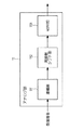
図1は、この発明装置の実施の形態1におけるOFDM(Orthogonal Frequency-Division Multiplexing)方式を用いたマルチチャネル受信装置1の構成を示すブロック図である。図1に示すように、受信信号が入力されるアナログ部11を備え、アナログ部11の出力部は複数の帯域の信号により構成される受信信号をA/D変換するA/D変換部(A/D変換手段)12に入力される。また、A/D変換部12にはA/D変換部12に対して供給するクロックの周波数を、所望の複数の帯域の信号の周波数配置に応じて、所定の周波数に制御して出力するクロック生成部(クロック生成手段)14の出力部も接続されており、A/D変換部12の出力部はA/D変換部12の出力から所望の複数の帯域の信号を取り出し、複数のデータを同時に再生する復調部(復調手段)13と接続される。復調部13は、データ♯1、データ♯2、…、データ♯nを出力する。
<
FIG. 1 is a block diagram showing a configuration of a
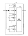
図2は、アナログ部11の構成を示すブロック図である。受信信号が入力される増幅器111を備え、増幅器111の出力部は周波数シフト部112の入力部に接続される。周波数シフト部112の出力部はMBPF(マルチバンドパスフィルタ)部113の入力部に接続され、MBPF部113の出力部がアナログ部11の出力部となる。
FIG. 2 is a block diagram showing a configuration of the analog unit 11. An
図4は上述したMBPF部113の構成を示すブロック図である。MBPF部113への入力部は並列に接続された複数のBPF(バンドバスフィルタ)部11311、11312、…、1131nに接続され、それぞれのBPF部の出力部は信号合成部1132に接続される。信号合成部1132の出力部が、MBPF部113の出力部となる。
FIG. 4 is a block diagram showing the configuration of the
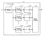
図3は、復調部13の構成を示すブロック図である。図1に示すようにA/D変換部12の出力部が復調部13の入力部に接続されており、復調部13の入力部は図3に示すように並列に接続された複数のリサンプラ部(リサンプル手段)1311、1312、…、131nに接続される。リサンプラ部1311の出力部はベースバンド変換部1321の入力部と接続され、ベースバンド変換部1321の出力部はLPF(ローパスフィルタ)部1331の入力部と接続される。LPF部1331の出力部はFFT部1341の入力部と接続され、FFT部1341の出力部は伝送路補正部1351の入力部に接続される。伝送路補正部1351の出力部はデマップ部1361の入力部に接続され、デマップ部1361の出力部は復調部13の出力部となる。
FIG. 3 is a block diagram showing a configuration of the
リサンプラ部1312についても、リサンプラ部1311と同様にベースバンド変換部1322、LPF部1332、FFT部1342、伝送路補正部1352、デマップ部1362の順に接続される。同様に、リサンプラ部1313、…、リサンプラ部131nについても、それぞれデマップ部1363、…、136nまで同様に接続される。従って、復調部13の出力部はデマップ部1361、デマップ部1362、…、デマップ部136nの出力部となる。
Similarly to the
次に本実施の形態に係るマルチチャネル受信装置1の動作について説明する。
Next, the operation of
図1において、複数の帯域の信号により構成される受信信号は、アナログ部11においてアナログ信号処理が行われ、A/D変換部12に入力される。A/D変換部12でデジタル変換された信号は復調部13に入力され、復調部13により帯域ごとに分離され、同時にデータの再生が行われる。また、クロック生成部14は、所望の複数の帯域の信号の周波数配置に応じて、クロック信号の周波数を所定の値に制御して、A/D変換部12に供給する。
In FIG. 1, a reception signal composed of signals in a plurality of bands is subjected to analog signal processing in an analog unit 11 and input to an A / D conversion unit 12. The signal digitally converted by the A / D converter 12 is input to the
次に、アナログ部11内部の動作について、図2を基に説明する。受信した信号は増幅器111に入力され、所望の信号電力の信号となるようにゲイン調整され、周波数シフト部112に出力される。周波数シフト部112では、受信した信号の中心周波数を所望の周波数に変換する。周波数シフト部112から出力された信号は、MBPF(マルチバンドパスフィルタ)部113に入力され、MBPF部113は多数の帯域の信号の中から複数の帯域の信号のみを通過させる。
Next, the operation inside the analog unit 11 will be described with reference to FIG. The received signal is input to the
すなわち、アナログ部11は複数の帯域の信号により構成される受信信号の一部の帯域を抑圧し、限られた複数の帯域の信号のみをA/D変換部12に対して出力する複数帯域通過手段となる。また、アナログ部11は、受信信号を通過させる帯域と抑圧する帯域が、ある所定の帯域の組み合わせになるように通過帯域と抑圧帯域を制御してもよい。 That is, the analog unit 11 suppresses a part of the band of the reception signal composed of signals of a plurality of bands, and outputs only a limited plurality of bands of signals to the A / D converter 12. It becomes a means. Further, the analog unit 11 may control the pass band and the suppression band so that the band through which the received signal is passed and the band to be suppressed are a combination of certain predetermined bands.
次に復調部13の動作について、図3を基に説明する。A/D変換部12によりデジタル化された信号は、リサンプラ部1311〜131nに入力され、受信した信号が所望のサンプルレートの信号に変換される。すなわちサンプルレート変換が行われる。リサンプラ部1311〜131nの出力はベースバンド変換部1321〜132nに入力され、受信したい帯域の信号の中心周波数がベースバンド周波数にシフトされ、I、Qの複素ベースバンド信号としてLPF(ローパスフィルタ)部1331〜133nに出力される。LPF部1331〜133nではベースバンド領域以外の不要の信号成分が抑圧され、ベースバンド領域の所望の信号のみが取り出され、FFT部1341〜134nに出力される。FFT部1341〜134nでは、入力されたI、Qのベースバンド信号が時間軸の信号から周波数軸の信号に変換され、その結果が伝送路補正部1351〜135nに出力される。
Next, the operation of the
伝送路補正部1351〜135nでは、入力された周波数軸信号から、伝送路による劣化が推定され、その劣化を補正した信号がデマップ部1361〜136nに供給される。デマップ部1361〜136nでは、入力された信号から、受信信号におけるBPSK、QPSK、16QAMなどの変調多値数に基づき、受信データが復元される。図3に示すように、リサンプラ部1311〜131n、ベースバンド変換部1321〜132n、LPF部1331〜133n、FFT部1341〜134n、伝送路補正部1351〜135n、デマップ部1361〜136nについて、それぞれの系列が並列に複数対備えるように接続されることによって、複数の帯域の信号を同時に復調することが可能となる。
In the transmission
ここで、アナログ部11中のMBPF部113は、全ての不要帯域信号を抑圧しなくてもよい。また、所望の複数信号の帯域によって、通過する帯域を可変にできる構成としてもよい。さらには、図4に示すように、MBPF部113は、複数のBPF(バンドパスフィルタ)部11311〜1131nと、これらの出力信号を合成する信号合成部1132によって構成されてもよい。すなわち、各々異なる周波数成分を通過させる複数のBPF部11311〜1131n、複数のBPF部11311〜1131nの複数の出力信号を合成する信号合成部1132を備える。このような構成により、周波数シフト部112でシフトする周波数幅とMBPF部113で通過する帯域設定の組み合わせにより、より柔軟に所望の帯域を選択することが可能となる。
Here, the
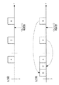
また、クロック生成部14からA/D変換部12に供給されるクロックの周波数と、所望の帯域の信号との関係が、図5に示すように、アンダーサンプルの関係であるものと、オーバーサンプルの関係であるものとが混在していてもよい。このような構成により、クロック生成部14において、A/D変換部12に供給されるクロック信号の周波数をより低く設定することができる。また、この場合、図5の帯域信号Cで示すように、信号成分が折りかえって、すなわち折返し歪みにより周波数の高低が逆転した帯域信号が入力するものが生じる。このため、復調部13は、このような信号成分をもう一度反転させて、本来の周波数の高低が逆転する前の帯域信号を正常にデータ再生する機能をもつものとする。
Further, as shown in FIG. 5, the relationship between the frequency of the clock supplied from the
また、復調部13は、図6に示すように、複数の所望の帯域の信号を再生する系で共通の1つのリサンプラ部の出力1311を使用する構成としてもよい。この場合、各帯域の信号を受信する系でサンプルレートが共通となるため、復調部13の各部で共通のクロック信号を使用することが可能となる。このクロック信号として、本来必要なクロック周波数の数倍の周波数のクロックを使い、各帯域の信号を受信する系の各ブロックでの処理をパラレル処理ではなく、各ブロックを共有したシリアル処理にすることによって、大幅に回路削減を行うこともできる。
Further, as shown in FIG. 6, the
本発明の効果として、クロック生成部14は、所望の複数の帯域の信号の周波数配置に応じて、クロック信号の周波数を所定の値に制御して、A/D変換部12に供給するため、A/D変換部12へ供給されるクロック信号の高速化を抑えることができ、エネルギー消費量やコストの増大、ジッタなどによる不安定な供給を回避することが可能である。
As an effect of the present invention, the
また、複数の帯域の信号を受信するために、一つのA/D変換部12しか使用しないので、大きく回路規模を縮小することができ、アナログ部11で不要信号を抑圧することによりA/D変換部12に供給されるクロック信号の高速化を低減することが可能である。 In addition, since only one A / D converter 12 is used to receive signals in a plurality of bands, the circuit scale can be greatly reduced, and the analog unit 11 can suppress unnecessary signals to reduce A / D. It is possible to reduce the speeding up of the clock signal supplied to the converter 12.
<実施の形態2>
実施の形態2におけるマルチチャネル受信装置2の全体図は図7で示されるように、実施の形態1と同様である。但し、実施の形態2においては、アナログ部(複数帯域通過手段)21の構成が実施の形態1とは異なる。図8にその構成を示す。受信信号が入力される増幅器211を備え、増幅器211の出力部は複数の帯域信号のそれぞれの中心周波数を周波数変換する複数の周波数シフト部(周波数シフト手段)2121〜212nの入力部に接続される。周波数シフト部2121〜212nの出力部は、周波数シフト部2121〜212nにより各々異なる中心周波数に変換された複数の信号において、各々異なる周波数成分を通過させる複数のBPF部(帯域通過手段)2131〜213nの入力部に接続される。複数のBPF部2131〜213nの出力部は、複数のBPF部2131〜213nの複数の出力信号を合成する信号合成部(信号合成手段)214の入力部に接続される。信号合成部214の出力部がアナログ部21の出力部となる。
<
The overall view of multi-channel receiving
次に、本実施の形態に係るマルチチャネル受信装置2の動作の説明を行う。
Next, the operation of multichannel receiving
受信信号はアナログ部21の増幅器211に入力され、所望の信号電力の信号となるようにゲイン調整され、所望の複数の帯域の信号に対応した周波数シフト部2121〜212nに出力される。周波数シフト部2121〜212nでは、受信した信号の中心周波数を所望の周波数に変換する。周波数シフト部2121〜212nから出力された信号は、所望の複数の帯域の信号に対応したBPF(バンドパスフィルタ)部2131〜213nに入力され、多数の帯域の信号の中から1つの帯域の信号のみを通過させる。
The received signal is input to the
ここで、実施の形態1と同様に、クロック生成部14からA/D変換部12に供給されるクロックの周波数と、所望の帯域の信号との関係が、図5に示すように、アンダーサンプルの関係であるものと、オーバーサンプルの関係であるものとが混在していてもよい。このような構成により、クロック生成部14において、A/D変換部12に供給されるクロック信号の周波数をより低く設定することができる。また、この場合も実施の形態1と同様に、図5の帯域信号Cで示すように、信号成分が折りかえって、周波数の高低が逆転するものが生じる場合がある。このため、復調部13は、このような信号成分をもう一度反転させて、正常にデータ再生する機能をもつものとする。
Here, as in the first embodiment, the relationship between the frequency of the clock supplied from the
また、復調部13は、図6に示す実施の形態1と同様に、各帯域の信号を受信する系で共通の1つのリサンプラ部1311の出力を使用する構成としてもよい。この場合、各帯域の信号を受信する系でサンプルレートが共通となるため、各部で共通のクロック信号を使用することが可能となる。このクロック信号として、本来必要なクロック周波数の数倍の周波数のクロックを使い、各帯域の信号を受信する系の各ブロックでの処理をパラレル処理ではなく、各ブロックを共有したシリアル処理にすることによって、大幅に回路削減を行うことができる。
Similarly to the first embodiment shown in FIG. 6, the
実施の形態2では、アナログ部21の構成は複雑になるが、所望の複数の帯域の信号に対応した周波数シフト部2121〜212nを備えることによって、所望の複数の帯域の信号を、低い周波数帯域に集中させることが可能となる。これにより、クロック生成部14からA/D変換部12に供給されるクロック信号の周波数をより低くできるメリットがある。
In the second embodiment, the configuration of the
なお、実施の形態1、実施の形態2では、OFDM信号によるマルチキャリアを用いたマルチチャネル受信装置について説明したが、本発明は、シングルキャリアを用いたマルチチャネル受信装置に適用する形態も可能である。
In
本発明の活用例として、デジタル放送受信装置や無線LAN受信装置に適用できる。 As an application example of the present invention, the present invention can be applied to a digital broadcast receiver or a wireless LAN receiver.
1 マルチチャネル受信装置、11 アナログ部、12 A/D変換部、13 復調部、14 クロック生成部、111 増幅器、112 周波数シフト部、113 MBPF部、1311〜131n リサンプラ部、1321〜132n ベースバンド変換部、1331〜133n LPF部、1341〜134n FFT部、1351〜135n 伝送路補正部、1361〜136n デマップ部、11311〜1131n BPF部、1132 信号合成部、2 マルチチャネル受信装置、21 アナログ部、211 増幅器、2121〜212n 周波数シフト部、2131〜213n BPF部、214 信号合成部。
DESCRIPTION OF
Claims (8)
前記A/D変換手段に対して供給するクロックの周波数を、所望の複数の帯域の信号の周波数配置に応じて、所定の周波数に制御して出力するクロック生成手段と、
前記A/D変換手段の出力から所望の複数の帯域の信号を取り出し、複数のデータを同時に再生する復調手段と、を備える、
マルチチャネル受信装置。 A / D conversion means for A / D converting a received signal composed of signals in a plurality of bands;
Clock generation means for controlling the frequency of the clock supplied to the A / D conversion means to a predetermined frequency according to the frequency arrangement of signals in a desired plurality of bands;
Demodulation means for extracting signals of a desired plurality of bands from the output of the A / D conversion means and reproducing a plurality of data simultaneously;
Multi-channel receiver.
請求項1に記載のマルチチャネル受信装置。 The relationship between the frequency of the clock supplied from the frequency clock generation means and the signal in the desired band is a mixture of an undersample relationship and an oversample relationship.
The multi-channel receiver according to claim 1.
請求項1または請求項2に記載のマルチチャネル受信装置。 The demodulating means normally reproduces data of the band signal before the original high and low frequency is reversed, even if a band signal whose frequency is reversed due to aliasing is input.
The multi-channel receiving device according to claim 1 or 2.
請求項1から請求項3のいずれかに記載のマルチチャネル受信装置。 The demodulating means includes resampling means for converting the sample rate of the output data of the A / D converting means, and the output of the resampling means is commonly used in a system for reproducing signals of a plurality of desired bands. ,
The multi-channel receiving device according to any one of claims 1 to 3.
請求項1から請求項4のいずれかに記載のマルチチャネル受信装置。 A plurality of band passing means for suppressing a part of the band of the received signal composed of signals of a plurality of bands and outputting only a limited plurality of bands of signals to the A / D conversion means;
The multi-channel receiving device according to any one of claims 1 to 4.
請求項5に記載のマルチチャネル受信装置。 The multiple band passing means controls the pass band and the suppression band so that the band for passing the received signal and the band to be suppressed are a combination of certain predetermined bands, and outputs the received signal.
The multi-channel receiving device according to claim 5.
各々異なる周波数成分を通過させる複数の帯域通過手段と、
前記複数の帯域通過手段の複数の出力信号を合成する信号合成手段と、を備える、
請求項5または請求項6に記載のマルチチャネル受信装置。 The multi-band passing means includes
A plurality of bandpass means for passing different frequency components,
Signal combining means for combining a plurality of output signals of the plurality of band-pass means,
The multi-channel receiver according to claim 5 or 6.
複数の帯域信号のそれぞれの中心周波数を周波数変換する複数の周波数シフト手段と、
前記周波数シフト手段により各々異なる中心周波数に変換された複数の信号において、各々異なる周波数成分を通過させる複数の帯域通過手段と、
前記複数の帯域通過手段の複数の出力信号を合成する信号合成手段と、を備える、
請求項5または請求項6に記載のマルチチャネル受信装置。 The multi-band passing means includes
A plurality of frequency shift means for converting the center frequency of each of the plurality of band signals;
A plurality of band pass means for passing different frequency components in a plurality of signals converted to different center frequencies by the frequency shift means;
Signal combining means for combining a plurality of output signals of the plurality of band-pass means,
The multi-channel receiver according to claim 5 or 6.
Priority Applications (1)
| Application Number | Priority Date | Filing Date | Title |
|---|---|---|---|
| JP2008296772A JP2010124302A (en) | 2008-11-20 | 2008-11-20 | Multichannel receiver |
Applications Claiming Priority (1)
| Application Number | Priority Date | Filing Date | Title |
|---|---|---|---|
| JP2008296772A JP2010124302A (en) | 2008-11-20 | 2008-11-20 | Multichannel receiver |
Publications (2)
| Publication Number | Publication Date |
|---|---|
| JP2010124302A true JP2010124302A (en) | 2010-06-03 |
| JP2010124302A5 JP2010124302A5 (en) | 2011-12-22 |
Family
ID=42325224
Family Applications (1)
| Application Number | Title | Priority Date | Filing Date |
|---|---|---|---|
| JP2008296772A Pending JP2010124302A (en) | 2008-11-20 | 2008-11-20 | Multichannel receiver |
Country Status (1)
| Country | Link |
|---|---|
| JP (1) | JP2010124302A (en) |
Citations (3)
| Publication number | Priority date | Publication date | Assignee | Title |
|---|---|---|---|---|
| JPH11136204A (en) * | 1997-08-29 | 1999-05-21 | Matsushita Electric Ind Co Ltd | Demodulator |
| JP2006086869A (en) * | 2004-09-16 | 2006-03-30 | Mitsubishi Electric Corp | Radio receiving device |
| WO2008047684A1 (en) * | 2006-10-17 | 2008-04-24 | Advantest Corporation | Measuring apparatus, measuring method, program and testing apparatus |
-
2008
- 2008-11-20 JP JP2008296772A patent/JP2010124302A/en active Pending
Patent Citations (3)
| Publication number | Priority date | Publication date | Assignee | Title |
|---|---|---|---|---|
| JPH11136204A (en) * | 1997-08-29 | 1999-05-21 | Matsushita Electric Ind Co Ltd | Demodulator |
| JP2006086869A (en) * | 2004-09-16 | 2006-03-30 | Mitsubishi Electric Corp | Radio receiving device |
| WO2008047684A1 (en) * | 2006-10-17 | 2008-04-24 | Advantest Corporation | Measuring apparatus, measuring method, program and testing apparatus |
Similar Documents
| Publication | Publication Date | Title |
|---|---|---|
| US7298715B2 (en) | Communication receiver with signal processing for beam forming and antenna diversity | |
| JP7304134B2 (en) | Method and Apparatus for Mixing Analog and Digital Audio for HD Radio Receiver | |
| US8630578B2 (en) | Methods and apparatus for interoperable satellite radio receivers | |
| JPH09266466A (en) | Digital transmission system | |
| JPH10224659A (en) | Orthogonal frequency division multiplex transmission system and transmission/reception device used for the same | |
| KR20090113915A (en) | Radio communication system | |
| JP2020184666A (en) | Transmitter and program | |
| JP6216511B2 (en) | Receiving device, semiconductor device, and receiving method | |
| JP4499045B2 (en) | OFDM demodulator, operation method of OFDM demodulator, program, and computer-readable recording medium | |
| JP2007235296A (en) | Ofdm signal receiver and receiving method, and digital broadcasting receiver | |
| JP5296183B2 (en) | Receiving apparatus and receiving method | |
| JP2010124302A (en) | Multichannel receiver | |
| JP2005136471A (en) | Ofdm receiver using diversity, ofdm reception circuit using diversity, and ofdm reception method using diversity | |
| US7852241B2 (en) | Demodulating apparatus, demodulating method, and computer-readable medium | |
| JP2003174390A (en) | Diversity receiver | |
| JP4684308B2 (en) | Demodulator | |
| JP5296182B2 (en) | Receiving apparatus and receiving method | |
| JP2006303718A (en) | Receiver and demodulating method | |
| JP2003218833A (en) | Ofdm receiver | |
| JPH0974366A (en) | Direct conversion receiver | |
| JP4541199B2 (en) | Receiver | |
| JP2007189316A (en) | Diversity receiver | |
| KR100801240B1 (en) | Send-receive equipment for method and send-receive equipment for multi-band orthogonal frequency division multiplexing communications | |
| JP6806497B2 (en) | Polarization shared converter, receiver and satellite receiver | |
| JP4245449B2 (en) | Diversity receiver |
Legal Events
| Date | Code | Title | Description |
|---|---|---|---|
| A521 | Written amendment |
Free format text: JAPANESE INTERMEDIATE CODE: A523 Effective date: 20111107 |
|
| A621 | Written request for application examination |
Free format text: JAPANESE INTERMEDIATE CODE: A621 Effective date: 20111107 |
|
| A977 | Report on retrieval |
Free format text: JAPANESE INTERMEDIATE CODE: A971007 Effective date: 20130115 |
|
| A131 | Notification of reasons for refusal |
Free format text: JAPANESE INTERMEDIATE CODE: A131 Effective date: 20130122 |
|
| A02 | Decision of refusal |
Free format text: JAPANESE INTERMEDIATE CODE: A02 Effective date: 20130521 |