JP2010103487A - Semiconductor laser device and display device - Google Patents
Semiconductor laser device and display device Download PDFInfo
- Publication number
- JP2010103487A JP2010103487A JP2009193795A JP2009193795A JP2010103487A JP 2010103487 A JP2010103487 A JP 2010103487A JP 2009193795 A JP2009193795 A JP 2009193795A JP 2009193795 A JP2009193795 A JP 2009193795A JP 2010103487 A JP2010103487 A JP 2010103487A
- Authority
- JP
- Japan
- Prior art keywords
- semiconductor laser
- laser element
- green
- red
- blue
- Prior art date
- Legal status (The legal status is an assumption and is not a legal conclusion. Google has not performed a legal analysis and makes no representation as to the accuracy of the status listed.)
- Pending
Links
- 239000004065 semiconductor Substances 0.000 title claims abstract description 698
- 230000017525 heat dissipation Effects 0.000 claims description 93
- 230000005855 radiation Effects 0.000 claims description 49
- 239000000758 substrate Substances 0.000 claims description 28
- 230000006866 deterioration Effects 0.000 abstract description 23
- 230000000630 rising effect Effects 0.000 abstract description 10
- 238000004020 luminiscence type Methods 0.000 abstract 1
- 239000010410 layer Substances 0.000 description 70
- 230000003287 optical effect Effects 0.000 description 22
- 239000002184 metal Substances 0.000 description 16
- 229910052751 metal Inorganic materials 0.000 description 16
- 230000004048 modification Effects 0.000 description 16
- 238000012986 modification Methods 0.000 description 16
- 230000004927 fusion Effects 0.000 description 15
- 238000005253 cladding Methods 0.000 description 14
- 238000000034 method Methods 0.000 description 14
- 239000004973 liquid crystal related substance Substances 0.000 description 13
- 230000010355 oscillation Effects 0.000 description 10
- 230000001902 propagating effect Effects 0.000 description 10
- 206010037660 Pyrexia Diseases 0.000 description 7
- JMASRVWKEDWRBT-UHFFFAOYSA-N Gallium nitride Chemical compound [Ga]#N JMASRVWKEDWRBT-UHFFFAOYSA-N 0.000 description 6
- 230000000694 effects Effects 0.000 description 5
- 229910001218 Gallium arsenide Inorganic materials 0.000 description 4
- 230000000903 blocking effect Effects 0.000 description 4
- 239000000463 material Substances 0.000 description 4
- 229910000679 solder Inorganic materials 0.000 description 4
- 150000004767 nitrides Chemical class 0.000 description 3
- 230000000644 propagated effect Effects 0.000 description 3
- 229910004298 SiO 2 Inorganic materials 0.000 description 2
- 230000004888 barrier function Effects 0.000 description 2
- 230000003111 delayed effect Effects 0.000 description 2
- 238000010586 diagram Methods 0.000 description 2
- 239000006185 dispersion Substances 0.000 description 2
- 238000009826 distribution Methods 0.000 description 2
- 238000005304 joining Methods 0.000 description 2
- 239000006096 absorbing agent Substances 0.000 description 1
- 238000005219 brazing Methods 0.000 description 1
- 239000000919 ceramic Substances 0.000 description 1
- 238000006243 chemical reaction Methods 0.000 description 1
- 239000003086 colorant Substances 0.000 description 1
- 229910052802 copper Inorganic materials 0.000 description 1
- 239000013078 crystal Substances 0.000 description 1
- 229910003460 diamond Inorganic materials 0.000 description 1
- 239000010432 diamond Substances 0.000 description 1
- 230000009977 dual effect Effects 0.000 description 1
- 230000020169 heat generation Effects 0.000 description 1
- 239000012212 insulator Substances 0.000 description 1
- 239000011159 matrix material Substances 0.000 description 1
- 239000002356 single layer Substances 0.000 description 1
- 229910052984 zinc sulfide Inorganic materials 0.000 description 1
Images

Classifications
-
- H—ELECTRICITY
- H04—ELECTRIC COMMUNICATION TECHNIQUE
- H04N—PICTORIAL COMMUNICATION, e.g. TELEVISION
- H04N9/00—Details of colour television systems
- H04N9/12—Picture reproducers
- H04N9/31—Projection devices for colour picture display, e.g. using electronic spatial light modulators [ESLM]
- H04N9/3141—Constructional details thereof
- H04N9/315—Modulator illumination systems
- H04N9/3161—Modulator illumination systems using laser light sources
-
- G—PHYSICS
- G03—PHOTOGRAPHY; CINEMATOGRAPHY; ANALOGOUS TECHNIQUES USING WAVES OTHER THAN OPTICAL WAVES; ELECTROGRAPHY; HOLOGRAPHY
- G03B—APPARATUS OR ARRANGEMENTS FOR TAKING PHOTOGRAPHS OR FOR PROJECTING OR VIEWING THEM; APPARATUS OR ARRANGEMENTS EMPLOYING ANALOGOUS TECHNIQUES USING WAVES OTHER THAN OPTICAL WAVES; ACCESSORIES THEREFOR
- G03B21/00—Projectors or projection-type viewers; Accessories therefor
- G03B21/14—Details
- G03B21/20—Lamp housings
- G03B21/2006—Lamp housings characterised by the light source
- G03B21/2033—LED or laser light sources
-
- H—ELECTRICITY
- H01—ELECTRIC ELEMENTS
- H01S—DEVICES USING THE PROCESS OF LIGHT AMPLIFICATION BY STIMULATED EMISSION OF RADIATION [LASER] TO AMPLIFY OR GENERATE LIGHT; DEVICES USING STIMULATED EMISSION OF ELECTROMAGNETIC RADIATION IN WAVE RANGES OTHER THAN OPTICAL
- H01S5/00—Semiconductor lasers
- H01S5/02—Structural details or components not essential to laser action
- H01S5/022—Mountings; Housings
- H01S5/023—Mount members, e.g. sub-mount members
- H01S5/02325—Mechanically integrated components on mount members or optical micro-benches
-
- H—ELECTRICITY
- H01—ELECTRIC ELEMENTS
- H01S—DEVICES USING THE PROCESS OF LIGHT AMPLIFICATION BY STIMULATED EMISSION OF RADIATION [LASER] TO AMPLIFY OR GENERATE LIGHT; DEVICES USING STIMULATED EMISSION OF ELECTROMAGNETIC RADIATION IN WAVE RANGES OTHER THAN OPTICAL
- H01S5/00—Semiconductor lasers
- H01S5/40—Arrangement of two or more semiconductor lasers, not provided for in groups H01S5/02 - H01S5/30
- H01S5/4025—Array arrangements, e.g. constituted by discrete laser diodes or laser bar
- H01S5/4031—Edge-emitting structures
-
- H—ELECTRICITY
- H04—ELECTRIC COMMUNICATION TECHNIQUE
- H04N—PICTORIAL COMMUNICATION, e.g. TELEVISION
- H04N9/00—Details of colour television systems
- H04N9/12—Picture reproducers
- H04N9/31—Projection devices for colour picture display, e.g. using electronic spatial light modulators [ESLM]
- H04N9/3102—Projection devices for colour picture display, e.g. using electronic spatial light modulators [ESLM] using two-dimensional electronic spatial light modulators
- H04N9/3105—Projection devices for colour picture display, e.g. using electronic spatial light modulators [ESLM] using two-dimensional electronic spatial light modulators for displaying all colours simultaneously, e.g. by using two or more electronic spatial light modulators
-
- H—ELECTRICITY
- H04—ELECTRIC COMMUNICATION TECHNIQUE
- H04N—PICTORIAL COMMUNICATION, e.g. TELEVISION
- H04N9/00—Details of colour television systems
- H04N9/12—Picture reproducers
- H04N9/31—Projection devices for colour picture display, e.g. using electronic spatial light modulators [ESLM]
- H04N9/3102—Projection devices for colour picture display, e.g. using electronic spatial light modulators [ESLM] using two-dimensional electronic spatial light modulators
- H04N9/3111—Projection devices for colour picture display, e.g. using electronic spatial light modulators [ESLM] using two-dimensional electronic spatial light modulators for displaying the colours sequentially, e.g. by using sequentially activated light sources
-
- H—ELECTRICITY
- H01—ELECTRIC ELEMENTS
- H01S—DEVICES USING THE PROCESS OF LIGHT AMPLIFICATION BY STIMULATED EMISSION OF RADIATION [LASER] TO AMPLIFY OR GENERATE LIGHT; DEVICES USING STIMULATED EMISSION OF ELECTROMAGNETIC RADIATION IN WAVE RANGES OTHER THAN OPTICAL
- H01S5/00—Semiconductor lasers
- H01S5/02—Structural details or components not essential to laser action
- H01S5/022—Mountings; Housings
- H01S5/02208—Mountings; Housings characterised by the shape of the housings
- H01S5/02212—Can-type, e.g. TO-CAN housings with emission along or parallel to symmetry axis
-
- H—ELECTRICITY
- H01—ELECTRIC ELEMENTS
- H01S—DEVICES USING THE PROCESS OF LIGHT AMPLIFICATION BY STIMULATED EMISSION OF RADIATION [LASER] TO AMPLIFY OR GENERATE LIGHT; DEVICES USING STIMULATED EMISSION OF ELECTROMAGNETIC RADIATION IN WAVE RANGES OTHER THAN OPTICAL
- H01S5/00—Semiconductor lasers
- H01S5/02—Structural details or components not essential to laser action
- H01S5/022—Mountings; Housings
- H01S5/0233—Mounting configuration of laser chips
- H01S5/0234—Up-side down mountings, e.g. Flip-chip, epi-side down mountings or junction down mountings
-
- H—ELECTRICITY
- H01—ELECTRIC ELEMENTS
- H01S—DEVICES USING THE PROCESS OF LIGHT AMPLIFICATION BY STIMULATED EMISSION OF RADIATION [LASER] TO AMPLIFY OR GENERATE LIGHT; DEVICES USING STIMULATED EMISSION OF ELECTROMAGNETIC RADIATION IN WAVE RANGES OTHER THAN OPTICAL
- H01S5/00—Semiconductor lasers
- H01S5/02—Structural details or components not essential to laser action
- H01S5/022—Mountings; Housings
- H01S5/0233—Mounting configuration of laser chips
- H01S5/02345—Wire-bonding
-
- H—ELECTRICITY
- H01—ELECTRIC ELEMENTS
- H01S—DEVICES USING THE PROCESS OF LIGHT AMPLIFICATION BY STIMULATED EMISSION OF RADIATION [LASER] TO AMPLIFY OR GENERATE LIGHT; DEVICES USING STIMULATED EMISSION OF ELECTROMAGNETIC RADIATION IN WAVE RANGES OTHER THAN OPTICAL
- H01S5/00—Semiconductor lasers
- H01S5/02—Structural details or components not essential to laser action
- H01S5/024—Arrangements for thermal management
- H01S5/02476—Heat spreaders, i.e. improving heat flow between laser chip and heat dissipating elements
- H01S5/02484—Sapphire or diamond heat spreaders
-
- H—ELECTRICITY
- H01—ELECTRIC ELEMENTS
- H01S—DEVICES USING THE PROCESS OF LIGHT AMPLIFICATION BY STIMULATED EMISSION OF RADIATION [LASER] TO AMPLIFY OR GENERATE LIGHT; DEVICES USING STIMULATED EMISSION OF ELECTROMAGNETIC RADIATION IN WAVE RANGES OTHER THAN OPTICAL
- H01S5/00—Semiconductor lasers
- H01S5/40—Arrangement of two or more semiconductor lasers, not provided for in groups H01S5/02 - H01S5/30
- H01S5/4025—Array arrangements, e.g. constituted by discrete laser diodes or laser bar
- H01S5/4087—Array arrangements, e.g. constituted by discrete laser diodes or laser bar emitting more than one wavelength
- H01S5/4093—Red, green and blue [RGB] generated directly by laser action or by a combination of laser action with nonlinear frequency conversion
Landscapes
- Physics & Mathematics (AREA)
- Optics & Photonics (AREA)
- Engineering & Computer Science (AREA)
- Multimedia (AREA)
- Signal Processing (AREA)
- General Physics & Mathematics (AREA)
- Condensed Matter Physics & Semiconductors (AREA)
- Electromagnetism (AREA)
- Projection Apparatus (AREA)
- Semiconductor Lasers (AREA)
Abstract
Description
本発明は、半導体レーザ装置および表示装置に関し、特に、赤色半導体レーザ素子と、緑色半導体レーザ素子と、青色半導体レーザ素子とを備える半導体レーザ装置およびそれを備える表示装置に関する。 The present invention relates to a semiconductor laser device and a display device, and more particularly to a semiconductor laser device including a red semiconductor laser element, a green semiconductor laser element, and a blue semiconductor laser element, and a display device including the same.
従来、赤色半導体レーザ素子と、緑色半導体レーザ素子と、青色半導体レーザ素子とを備える半導体レーザ装置が知られている(たとえば、特許文献1参照)。 Conventionally, a semiconductor laser device including a red semiconductor laser element, a green semiconductor laser element, and a blue semiconductor laser element is known (see, for example, Patent Document 1).
上記特許文献1に記載のレーザ光源(半導体レーザ装置)では、単一のパッケージ(ステム)の上に接合された単一の支持基板(放熱基台)の表面上に、赤色半導体レーザ素子、緑色半導体レーザ素子および青色半導体レーザ素子がこの順番で所定の間隔を隔てて平面的に配置されている。すなわち、赤色半導体レーザ素子と緑色半導体レーザ素子とが隣接するように配置されている。また、赤色半導体レーザ素子、緑色半導体レーザ素子および青色半導体レーザ素子は、それぞれ、ろう材により、導電性の金属層によって被覆された支持基板にジャンクションダウン方式で接合されている。
In the laser light source (semiconductor laser device) described in
ここで、緑色半導体レーザ素子は発光効率(エネルギー変換効率)が悪いため、緑色半導体レーザ素子が赤色半導体レーザ素子および青色半導体レーザ素子と同程度の発光強度を得るためには、緑色半導体レーザ素子に対して赤色半導体レーザ素子および青色半導体レーザ素子よりも、より多くの電力を供給する必要がある。したがって、半導体レーザ装置の動作時に、緑色半導体レーザ素子からの発熱量は、赤色半導体レーザ素子および青色半導体レーザ素子からの発熱量と比べて大きくなる。 Here, since the green semiconductor laser element has low emission efficiency (energy conversion efficiency), in order for the green semiconductor laser element to obtain the same emission intensity as the red semiconductor laser element and the blue semiconductor laser element, On the other hand, it is necessary to supply more electric power than the red semiconductor laser element and the blue semiconductor laser element. Therefore, during operation of the semiconductor laser device, the amount of heat generated from the green semiconductor laser element is larger than the amount of heat generated from the red semiconductor laser element and the blue semiconductor laser element.
一方、発振波長の長い赤色半導体レーザ素子は、発振波長の短い青色半導体レーザ素子および緑色半導体レーザ素子と比べて、バンドギャップが小さい材料からなる。このため、赤色半導体レーザ素子において、温度の上昇によって増加する閾値電流の増加量が、青色半導体レーザ素子および緑色半導体レーザ素子における閾値電流の増加量と比べて大きくなる。したがって、赤色半導体レーザ素子では、青色半導体レーザ素子および緑色半導体レーザ素子と比べて、閾値電流の増加に伴って増加する動作電流の増加量が大きいため、温度上昇に起因して発光特性がより劣化しやすい。 On the other hand, the red semiconductor laser element having a long oscillation wavelength is made of a material having a smaller band gap than the blue semiconductor laser element and the green semiconductor laser element having a short oscillation wavelength. For this reason, in the red semiconductor laser element, the amount of increase in the threshold current that increases as the temperature rises is larger than the amount of increase in the threshold current in the blue semiconductor laser element and the green semiconductor laser element. Therefore, the red semiconductor laser device has a larger increase in operating current as the threshold current increases than the blue semiconductor laser device and the green semiconductor laser device. It's easy to do.
しかしながら、上記特許文献1に開示されたレーザ光源では、赤色半導体レーザ素子が、緑色半導体レーザ素子と隣接するように単一の支持基板の表面上に接合されていることによって、両者を略同時または時系列的に交互に発振させた場合に、発熱量の大きい緑色半導体レーザ素子から支持基板を介して赤色半導体レーザ素子に熱が伝播する。このため、レーザ光源の動作時に、赤色半導体レーザ素子の温度が上昇することによって、赤色半導体レーザ素子の動作電流が大きくなる。したがって、赤色半導体レーザ素子の発光特性が劣化するという問題点がある。
However, in the laser light source disclosed in
この発明は、上記のような課題を解決するためになされたものであり、この発明の1つの目的は、半導体レーザ装置の動作時に、赤色半導体レーザ素子の温度が上昇することに起因する発光特性の劣化を抑制することが可能な半導体レーザ装置および表示装置を提供することである。 The present invention has been made to solve the above-described problems, and one object of the present invention is to provide light emission characteristics resulting from an increase in temperature of a red semiconductor laser element during operation of a semiconductor laser device. It is an object to provide a semiconductor laser device and a display device capable of suppressing deterioration of the semiconductor device.
上記目的を達成するために、この発明の第1の局面による半導体レーザ装置は、赤色半導体レーザ素子と、緑色半導体レーザ素子と、青色半導体レーザ素子とを備え、赤色半導体レーザ素子、緑色半導体レーザ素子および青色半導体レーザ素子の各々が電力を供給するためのワイヤに個別に接続された状態で単一のパッケージ内に配置され、かつ、レーザ光の出射方向から見て、赤色半導体レーザ素子と緑色半導体レーザ素子との間に青色半導体レーザ素子が配置されている。 In order to achieve the above object, a semiconductor laser device according to a first aspect of the present invention includes a red semiconductor laser element, a green semiconductor laser element, and a blue semiconductor laser element. And the blue semiconductor laser element are disposed in a single package in a state of being individually connected to wires for supplying electric power, and viewed from the laser light emission direction, the red semiconductor laser element and the green semiconductor laser A blue semiconductor laser element is disposed between the laser elements.
この発明の第1の局面による半導体レーザ装置では、上記のように、赤色半導体レーザ素子と緑色半導体レーザ素子との間に青色半導体レーザ素子を配置することによって、発熱量の大きい緑色半導体レーザ素子からの熱が、赤色半導体レーザ素子に伝播するのを低減することができるので、半導体レーザ装置の動作時に、赤色半導体レーザ素子の温度が上昇することに起因する発光特性の劣化を抑制することができる。また、赤色半導体レーザ素子、緑色半導体レーザ素子および青色半導体レーザ素子の各々を電力を供給するためのワイヤに個別に接続された状態で配置することによって、各々のレーザ素子に個別に接続されたワイヤの部分から各々のレーザ素子が発生する熱を放出させることができるので、これによっても、半導体レーザ装置の動作時に、赤色半導体レーザ素子の温度が上昇することに起因する発光特性の劣化を抑制することができる。 In the semiconductor laser device according to the first aspect of the present invention, as described above, by disposing the blue semiconductor laser element between the red semiconductor laser element and the green semiconductor laser element, Can be prevented from propagating to the red semiconductor laser element, so that it is possible to suppress the deterioration of the light emission characteristics caused by the temperature rise of the red semiconductor laser element during the operation of the semiconductor laser device. . Further, by arranging each of the red semiconductor laser element, the green semiconductor laser element, and the blue semiconductor laser element in a state of being individually connected to a wire for supplying electric power, the wire individually connected to each laser element Since the heat generated by each laser element can be released from this portion, this also suppresses the deterioration of the light emission characteristics caused by the temperature rise of the red semiconductor laser element during the operation of the semiconductor laser device. be able to.
この発明の第2の局面による半導体レーザ装置は、第1発光部を有する赤色半導体レーザ素子と、第2発光部を有する緑色半導体レーザ素子と、第3発光部を有する青色半導体レーザ素子と、赤色半導体レーザ素子、緑色半導体レーザ素子および青色半導体レーザ素子が配置された支持基体を有するパッケージとを備え、レーザ光の出射方向から見て、赤色半導体レーザ素子と緑色半導体レーザ素子との間に青色半導体レーザ素子が配置され、第1発光部、第2発光部および第3発光部がそれぞれ支持基体側になるように配置されている。 A semiconductor laser device according to a second aspect of the present invention includes a red semiconductor laser element having a first light emitting portion, a green semiconductor laser element having a second light emitting portion, a blue semiconductor laser element having a third light emitting portion, and a red color. A semiconductor laser element, a green semiconductor laser element, and a package having a support base on which the blue semiconductor laser element is arranged, and a blue semiconductor between the red semiconductor laser element and the green semiconductor laser element when viewed from the laser beam emitting direction. A laser element is disposed, and the first light emitting unit, the second light emitting unit, and the third light emitting unit are disposed on the support base side.
この発明の第2の局面による半導体レーザ装置では、上記のように、赤色半導体レーザ素子と緑色半導体レーザ素子との間に青色半導体レーザ素子を配置することによって、発熱量の大きい緑色半導体レーザ素子からの熱が、赤色半導体レーザ素子に伝播するのを低減することができるので、半導体レーザ装置の動作時に、赤色半導体レーザ素子の温度が上昇することに起因する発光特性の劣化を抑制することができる。また、第1発光部、第2発光部および第3発光部をそれぞれ支持基体側になるように配置することによって、赤色半導体レーザ素子の第1発光部において発生する熱と、緑色半導体レーザ素子の第2発光部において発生する熱と、青色半導体レーザ素子の第3発光部において発生する熱とを、容易に、第1発光部、第2発光部および第3発光部の近傍に位置する支持基体から放出させることができる。これにより、緑色半導体レーザ素子および青色半導体レーザ素子からの熱が、赤色半導体レーザ素子に伝播するのをより低減することができるとともに、赤色半導体レーザ素子の第1発光部において発生する熱を支持基体において放出させることができるので、これによっても、半導体レーザ装置の動作時に、赤色半導体レーザ素子の温度が上昇することに起因する発光特性の劣化を抑制することができる。 In the semiconductor laser device according to the second aspect of the present invention, as described above, by disposing the blue semiconductor laser element between the red semiconductor laser element and the green semiconductor laser element, Can be prevented from propagating to the red semiconductor laser element, so that it is possible to suppress the deterioration of the light emission characteristics caused by the temperature rise of the red semiconductor laser element during the operation of the semiconductor laser device. . Further, by arranging the first light emitting unit, the second light emitting unit, and the third light emitting unit so as to be on the support base side, the heat generated in the first light emitting unit of the red semiconductor laser element and the green semiconductor laser element A support base that is easily located in the vicinity of the first light-emitting part, the second light-emitting part, and the third light-emitting part with the heat generated in the second light-emitting part and the heat generated in the third light-emitting part of the blue semiconductor laser element Can be released from Accordingly, the heat from the green semiconductor laser element and the blue semiconductor laser element can be further reduced from propagating to the red semiconductor laser element, and the heat generated in the first light emitting unit of the red semiconductor laser element can be reduced. Therefore, it is possible to suppress the deterioration of the light emission characteristics caused by the temperature rise of the red semiconductor laser element during the operation of the semiconductor laser device.
上記第1および第2の局面による半導体レーザ装置において、好ましくは、赤色半導体レーザ素子は、GaAs基板上に形成されているとともに、緑色半導体レーザ素子および青色半導体レーザ素子は、それぞれ、窒化物系半導体を含む材料により構成されている。このように構成すれば、本発明の半導体レーザ装置を構成する赤色半導体レーザ素子と、緑色半導体レーザ素子および青色半導体レーザ素子とを容易に形成することができる。 In the semiconductor laser device according to the first and second aspects, preferably, the red semiconductor laser element is formed on a GaAs substrate, and the green semiconductor laser element and the blue semiconductor laser element are respectively nitride-based semiconductors. It is comprised with the material containing. If comprised in this way, the red semiconductor laser element which comprises the semiconductor laser apparatus of this invention, a green semiconductor laser element, and a blue semiconductor laser element can be formed easily.
上記第1の局面による半導体レーザ装置において、好ましくは、パッケージは、赤色半導体レーザ素子、緑色半導体レーザ素子および青色半導体レーザ素子が配置された支持基体を有する。このように構成すれば、支持基体によって、赤色半導体レーザ素子、緑色半導体レーザ素子および青色半導体レーザ素子の各々において発生した熱を外部に放出することができる。 In the semiconductor laser device according to the first aspect, preferably, the package has a support base on which the red semiconductor laser element, the green semiconductor laser element, and the blue semiconductor laser element are arranged. If comprised in this way, the heat | fever which generate | occur | produced in each of a red semiconductor laser element, a green semiconductor laser element, and a blue semiconductor laser element can be discharge | released outside by a support base.
上記パッケージが支持基体を有する半導体レーザ装置において、好ましくは、赤色半導体レーザ素子は、支持基体側に形成された第1発光部を有する。このように構成すれば、赤色半導体レーザ素子の第1発光部において発生する熱を、容易に、赤色半導体レーザ素子の第1発光部の近傍に設けられた支持基体から放出させることができるので、半導体レーザ装置の動作時に、赤色半導体レーザ素子の温度が上昇することに起因する発光特性の劣化をより抑制することができる。 In the semiconductor laser device in which the package has a support base, preferably, the red semiconductor laser element has a first light emitting portion formed on the support base. If comprised in this way, since the heat | fever generate | occur | produced in the 1st light emission part of a red semiconductor laser element can be easily discharge | released from the support base | substrate provided in the vicinity of the 1st light emission part of a red semiconductor laser element, During the operation of the semiconductor laser device, it is possible to further suppress the deterioration of the light emission characteristics caused by the temperature of the red semiconductor laser element rising.
上記パッケージが支持基体を有する半導体レーザ装置において、好ましくは、赤色半導体レーザ素子と支持基体との間に配置される第1放熱基台と、緑色半導体レーザ素子および青色半導体レーザ素子と支持基体との間に配置される少なくとも1つの第2放熱基台とをさらに備え、第1放熱基台は、第2放熱基台から分離されている。このように構成すれば、緑色半導体レーザ素子および青色半導体レーザ素子からの熱が、第2放熱基台および第1放熱基台を介して、赤色半導体レーザ素子に伝播するのを低減することができる。また、赤色半導体レーザ素子において発生する熱を、第1放熱基台から放出させることができるとともに、緑色半導体レーザ素子および青色半導体レーザ素子において発生する熱を、第2放熱基台から放出させることができる。これらにより、半導体レーザ装置の動作時に、赤色半導体レーザ素子の温度が上昇することに起因する発光特性の劣化をより抑制することができる。 In the semiconductor laser device in which the package has a supporting base, preferably, a first heat radiation base disposed between the red semiconductor laser element and the supporting base, a green semiconductor laser element, a blue semiconductor laser element, and the supporting base And at least one second heat dissipation base disposed between the first heat dissipation base and the second heat dissipation base. If comprised in this way, it can reduce that the heat | fever from a green semiconductor laser element and a blue semiconductor laser element propagates to a red semiconductor laser element via a 2nd thermal radiation base and a 1st thermal radiation base. . In addition, heat generated in the red semiconductor laser element can be released from the first heat dissipation base, and heat generated in the green semiconductor laser element and the blue semiconductor laser element can be released from the second heat dissipation base. it can. Accordingly, it is possible to further suppress the deterioration of the light emission characteristics due to the temperature of the red semiconductor laser element rising during the operation of the semiconductor laser device.
この場合、好ましくは、第1放熱基台の熱伝導率は、第2放熱基台の熱伝導率よりも大きい。このように構成すれば、第1放熱基台において赤色半導体レーザ素子から支持基体への放熱を効率よく行うことができる。また、第2放熱基台において緑色半導体レーザ素子および青色半導体レーザ素子から支持基体へ熱が伝達されるのをある程度遅らせることができる。したがって、赤色半導体レーザ素子に熱をより伝播させにくくすることができる。 In this case, preferably, the thermal conductivity of the first heat radiation base is larger than the heat conductivity of the second heat radiation base. If comprised in this way, in the 1st heat dissipation base, heat dissipation from a red semiconductor laser element to a support base | substrate can be performed efficiently. In addition, heat transfer from the green semiconductor laser element and the blue semiconductor laser element to the support base can be delayed to some extent in the second heat dissipation base. Therefore, it is possible to make it difficult for heat to propagate to the red semiconductor laser element.
上記第1放熱基台が第2放熱基台から分離されている半導体レーザ装置において、好ましくは、第2放熱基台は、緑色半導体レーザ素子と支持基体との間に配置される第3放熱基台と、青色半導体レーザ素子と支持基体との間に配置され、第3放熱基台と分離された第4放熱基台とを含む。このように構成すれば、緑色半導体レーザ素子において発生する熱と青色半導体レーザ素子において発生する熱とを、第3放熱基台および第4放熱基台において別々に放出させることができるので、赤色半導体レーザ素子に熱をさらに伝播させにくくすることができる。 In the semiconductor laser device in which the first heat dissipation base is separated from the second heat dissipation base, preferably, the second heat dissipation base is a third heat dissipation base disposed between the green semiconductor laser element and the support base. And a fourth heat radiating base disposed between the blue semiconductor laser element and the support base and separated from the third heat radiating base. With this configuration, the heat generated in the green semiconductor laser element and the heat generated in the blue semiconductor laser element can be separately released in the third heat dissipation base and the fourth heat dissipation base. Heat can be further prevented from propagating to the laser element.
上記第1放熱基台が第2放熱基台から分離されている半導体レーザ装置において、好ましくは、支持基体は、第1放熱基台が配置された部分と第2放熱基台が配置された部分との間に溝部を有する。このように構成すれば、支持基体の溝部によって、緑色半導体レーザ素子および青色半導体レーザ素子からの熱が赤色半導体レーザ素子に伝播するのを一層低減することができる。 In the semiconductor laser device in which the first heat dissipation base is separated from the second heat dissipation base, preferably, the support base is a portion where the first heat dissipation base is disposed and a portion where the second heat dissipation base is disposed. A groove between the two. If comprised in this way, it can further reduce that the heat | fever from a green semiconductor laser element and a blue semiconductor laser element propagates to a red semiconductor laser element by the groove part of a support base | substrate.
上記第1放熱基台が第2放熱基台から分離されている半導体レーザ装置において、好ましくは、支持基体は、第1放熱基台が配置される第1支持基体と、第2放熱基台が配置され、第1支持基体と分離された第2支持基体とを有する。このように構成すれば、第1放熱基台が第2放熱基台から分離されているのみならず、第1放熱基台が配置される第1支持基体と第2放熱基台が配置される第2支持基体とも分離されているので、緑色半導体レーザ素子および青色半導体レーザ素子からの熱が赤色半導体レーザ素子に伝播するのをより一層低減することができる。 In the semiconductor laser device in which the first heat dissipation base is separated from the second heat dissipation base, preferably, the support base includes a first support base on which the first heat dissipation base is disposed, and a second heat dissipation base. A second support substrate is disposed and separated from the first support substrate. If comprised in this way, not only the 1st heat dissipation base will be isolate | separated from the 2nd heat dissipation base but the 1st support base | substrate and 2nd heat dissipation base in which a 1st heat dissipation base will be arrange | positioned are arrange | positioned. Since the second support base is also separated, it is possible to further reduce the propagation of heat from the green semiconductor laser element and the blue semiconductor laser element to the red semiconductor laser element.
上記パッケージが支持基体を有する半導体レーザ装置において、好ましくは、緑色半導体レーザ素子および青色半導体レーザ素子は、それぞれ、第2発光部および第3発光部を有し、第2発光部および第3発光部は、それぞれ、支持基体側になるように配置されている。このように構成すれば、緑色半導体レーザ素子の第2発光部において発生する熱と、青色半導体レーザ素子の第3発光部において発生する熱とを、第2発光部および第3発光部の近傍に位置する支持基体から容易に放出させることができる。 In the semiconductor laser device in which the package has a supporting base, preferably, the green semiconductor laser element and the blue semiconductor laser element have a second light emitting part and a third light emitting part, respectively, and the second light emitting part and the third light emitting part, respectively. Are arranged on the support base side. If comprised in this way, the heat | fever which generate | occur | produces in the 2nd light emission part of a green semiconductor laser element, and the heat | fever which generate | occur | produces in the 3rd light emission part of a blue semiconductor laser element are made into the vicinity of a 2nd light emission part and a 3rd light emission part. It can be easily released from the support substrate located.
上記第1放熱基台が第2放熱基台から分離されている半導体レーザ装置において、好ましくは、赤色半導体レーザ素子、緑色半導体レーザ素子および青色半導体レーザ素子は、それぞれ、第1発光部、第2発光部および第3発光部を有し、第1発光部は、第1放熱基台側になるように配置されているとともに、第2発光部および第3発光部は、それぞれ、第2放熱基台側になるように配置されている。このように構成すれば、赤色半導体レーザ素子の第1発光部において発生する熱を、第1発光部の近傍に位置する第1放熱基台および支持基体から容易に放出させることができるとともに、緑色半導体レーザ素子の第2発光部において発生する熱と、青色半導体レーザ素子の第3発光部において発生する熱とを、第2発光部および第3発光部の近傍に位置する第2放熱基台および支持基体から容易に放出させることができる。 In the semiconductor laser device in which the first heat radiating base is separated from the second heat radiating base, preferably, the red semiconductor laser element, the green semiconductor laser element, and the blue semiconductor laser element include the first light emitting unit and the second light emitting unit, respectively. The light emitting unit and the third light emitting unit are disposed, the first light emitting unit is disposed on the first heat dissipating base side, and the second light emitting unit and the third light emitting unit are respectively provided with the second heat dissipating group. It is arranged to be on the table side. With this configuration, the heat generated in the first light emitting portion of the red semiconductor laser element can be easily released from the first heat radiation base and the support base located in the vicinity of the first light emitting portion, and the green A second heat dissipating base located near the second light emitting unit and the third light emitting unit, and heat generated in the second light emitting unit of the semiconductor laser element and heat generated in the third light emitting unit of the blue semiconductor laser element; It can be easily released from the support substrate.
上記第1放熱基台が第2放熱基台から分離されている半導体レーザ装置において、好ましくは、パッケージ、第1放熱基台および第2放熱基台は、それぞれ、導電性を有する。このように構成すれば、パッケージと、赤色半導体レーザ素子の一方電極、緑色半導体レーザ素子の一方電極および青色半導体レーザ素子の一方電極とを接続するためのワイヤが不要になるので、半導体レーザ装置におけるワイヤ配線が複雑化するのを抑制することができる。 In the semiconductor laser device in which the first heat dissipation base is separated from the second heat dissipation base, preferably, the package, the first heat dissipation base, and the second heat dissipation base each have conductivity. This configuration eliminates the need for a wire for connecting the package to one electrode of the red semiconductor laser element, one electrode of the green semiconductor laser element, and one electrode of the blue semiconductor laser element. It is possible to prevent the wire wiring from becoming complicated.
上記パッケージが支持基体を有する半導体レーザ装置において、好ましくは、赤色半導体レーザ素子、緑色半導体レーザ素子および青色半導体レーザ素子の支持基体側と反対側の電極には、それぞれ、ワイヤが接続されている。このように構成すれば、電力を供給するための配線の自由度を大きくすることができるとともに、各々のレーザ素子において発生する熱を、各々に接続されたワイヤを介して放出させることができる。 In the semiconductor laser device in which the package has a support base, wires are preferably connected to the electrodes on the opposite side of the support base of the red semiconductor laser element, the green semiconductor laser element, and the blue semiconductor laser element, respectively. With this configuration, the degree of freedom of wiring for supplying electric power can be increased, and heat generated in each laser element can be released through the wire connected to each laser element.
上記第1および第2の局面による半導体レーザ装置において、好ましくは、緑色半導体レーザ素子および青色半導体レーザ素子は、同一の基板の表面上に形成されている。このように構成すれば、緑色半導体レーザ素子と青色半導体レーザ素子とを別々に固定する必要がないので、緑色半導体レーザ素子の発光点と、青色半導体レーザ素子の発光点との間隔をより正確に位置決めすることができる。 In the semiconductor laser device according to the first and second aspects, the green semiconductor laser element and the blue semiconductor laser element are preferably formed on the surface of the same substrate. With this configuration, it is not necessary to fix the green semiconductor laser element and the blue semiconductor laser element separately, so that the distance between the emission point of the green semiconductor laser element and the emission point of the blue semiconductor laser element can be more accurately determined. Can be positioned.
上記パッケージが支持基体を有する半導体レーザ装置において、好ましくは、赤色半導体レーザ素子と緑色半導体レーザ素子とは、それぞれ、支持基体の両端部近傍に配置されている。このように構成すれば、赤色半導体レーザ素子と緑色半導体レーザ素子との間隔を大きくすることができるので、発熱量の大きい緑色半導体レーザ素子からの熱が、赤色半導体レーザ素子に伝播するのをより低減することができるとともに、赤色半導体レーザ素子の温度が上昇することに起因する発光特性の劣化をより抑制することができる。 In the semiconductor laser device in which the package has a support base, preferably, the red semiconductor laser element and the green semiconductor laser element are respectively disposed in the vicinity of both ends of the support base. With this configuration, the distance between the red semiconductor laser element and the green semiconductor laser element can be increased, so that the heat from the green semiconductor laser element having a large calorific value is more propagated to the red semiconductor laser element. While being able to reduce, the deterioration of the light emission characteristic resulting from the temperature rise of a red semiconductor laser element can be suppressed more.
上記第1および第2の局面による半導体レーザ装置において、好ましくは、赤色半導体レーザ素子は、単一のパッケージ内に複数個配置され、複数の赤色半導体レーザ素子は、それぞれ、緑色半導体レーザ素子と隣り合わないようにパッケージ内に配置されている。このように構成すれば、発熱量の大きい緑色半導体レーザ素子からの熱が、緑色半導体レーザ素子と隣り合わないように複数配置された赤色半導体レーザ素子の各々に伝播するのを低減することができるので、半導体レーザ装置の動作時に、各々の赤色半導体レーザ素子の温度が上昇することに起因する発光特性の劣化を抑制することができる。 In the semiconductor laser device according to the first and second aspects, preferably, a plurality of red semiconductor laser elements are arranged in a single package, and each of the plurality of red semiconductor laser elements is adjacent to the green semiconductor laser element. It is arranged in the package so that it does not fit. If comprised in this way, it can reduce that the heat | fever from the green semiconductor laser element with a large emitted-heat amount propagates to each of the red semiconductor laser element arrange | positioned so that it may not adjoin a green semiconductor laser element. Therefore, it is possible to suppress the deterioration of the light emission characteristics caused by the temperature of each red semiconductor laser element rising during the operation of the semiconductor laser device.
上記第1および第2の局面による半導体レーザ装置において、好ましくは、緑色半導体レーザ素子および青色半導体レーザ素子は、共通の一方電極を有する。このように構成すれば、緑色半導体レーザ素子の一方電極および青色半導体レーザ素子の一方電極に共通の電源を接続して、緑色半導体レーザ素子および青色半導体レーザ素子を駆動させることができる。 In the semiconductor laser devices according to the first and second aspects, preferably, the green semiconductor laser element and the blue semiconductor laser element have a common one electrode. If comprised in this way, a common power supply can be connected to one electrode of a green semiconductor laser element, and one electrode of a blue semiconductor laser element, and a green semiconductor laser element and a blue semiconductor laser element can be driven.
上記第1および第2の局面による半導体レーザ装置において、好ましくは、緑色半導体レーザ素子および青色半導体レーザ素子は、それぞれ、支持基体側とは反対側に形成された第2発光部および第3発光部を有する。このように構成すれば、支持基体側に第2発光部および第3発光部が配置される場合と比べて、第2発光部および第3発光部を支持基体から遠ざけることができるので、第2発光部および第3発光部において発生した熱が、支持基体を介して赤色半導体レーザ素子に伝播するのをより低減することができる。 In the semiconductor laser device according to the first and second aspects, preferably, the green semiconductor laser element and the blue semiconductor laser element are a second light emitting part and a third light emitting part formed on the side opposite to the support base side, respectively. Have If comprised in this way, since the 2nd light emission part and the 3rd light emission part can be kept away from a support base compared with the case where the 2nd light emission part and the 3rd light emission part are arranged at the support base side, the 2nd It is possible to further reduce the heat generated in the light emitting unit and the third light emitting unit from propagating to the red semiconductor laser element through the support base.
この発明の第3の局面による表示装置は、赤色半導体レーザ素子と、緑色半導体レーザ素子と、青色半導体レーザ素子とを含み、赤色半導体レーザ素子、緑色半導体レーザ素子および青色半導体レーザ素子が単一のパッケージ内に配置され、かつ、レーザ光の出射方向から見て、赤色半導体レーザ素子と緑色半導体レーザ素子との間に青色半導体レーザ素子が配置されている半導体レーザ装置と、半導体レーザ装置からの光の変調を行う変調手段とを備える。 A display device according to a third aspect of the present invention includes a red semiconductor laser element, a green semiconductor laser element, and a blue semiconductor laser element, wherein the red semiconductor laser element, the green semiconductor laser element, and the blue semiconductor laser element are single. A semiconductor laser device arranged in a package and having a blue semiconductor laser device arranged between the red semiconductor laser device and the green semiconductor laser device when viewed from the laser beam emitting direction; and light from the semiconductor laser device Modulation means for performing the above modulation.
この発明の第3の局面による表示装置では、上記のように、赤色半導体レーザ素子と緑色半導体レーザ素子との間に青色半導体レーザ素子を配置することによって、発熱量の大きい緑色半導体レーザ素子からの熱が、赤色半導体レーザ素子に伝播するのを低減することができるので、半導体レーザ装置の動作時に、赤色半導体レーザ素子の温度が上昇することに起因する発光特性の劣化を抑制することができる半導体レーザ装置を用いて、変調手段により光を変調させて所望の画像を表示させることができる。 In the display device according to the third aspect of the present invention, as described above, by disposing the blue semiconductor laser element between the red semiconductor laser element and the green semiconductor laser element, Since it is possible to reduce the propagation of heat to the red semiconductor laser element, a semiconductor capable of suppressing the deterioration of the light emission characteristics due to the temperature of the red semiconductor laser element rising during the operation of the semiconductor laser device Using a laser device, it is possible to display a desired image by modulating light by a modulating means.
上記第3の局面による表示装置において、好ましくは、赤色半導体レーザ素子、緑色半導体レーザ素子および青色半導体レーザ素子を、略同時に発振するか、または時系列的に交互に発振するように構成されている。なお、「略同時に発振する」とは、一方の半導体レーザ素子が発振している間に、他の半導体レーザ素子が発振していればよく、必ずしも赤色半導体レーザ素子、緑色半導体レーザ素子および青色半導体レーザ素子の発振の開始が一致している必要はない。このように赤色半導体レーザ素子、緑色半導体レーザ素子および青色半導体レーザ素子を略同時または時系列的に交互に発振する場合には、それぞれ個別に発振させる場合と比べて、発振させているレーザ素子の数や合計発振時間が増加するので、赤色半導体レーザ素子、緑色半導体レーザ素子および青色半導体レーザ素子を駆動させることにより発生する合計の熱量が大きくなる。この場合に、赤色半導体レーザ素子と緑色半導体レーザ素子とを隣り合わないように配置することによって、発熱量の大きい緑色半導体レーザ素子からの熱が、赤色半導体レーザ素子に伝播するのを低減することができるので、半導体レーザ装置の動作時に、赤色半導体レーザ素子の温度が上昇することに起因する発光特性の劣化を有効に抑制することができる表示装置を得ることができる。 In the display device according to the third aspect, the red semiconductor laser element, the green semiconductor laser element, and the blue semiconductor laser element are preferably configured to oscillate substantially simultaneously or alternately in time series. . Note that “oscillate substantially at the same time” means that one semiconductor laser element oscillates while the other semiconductor laser element oscillates, and is not necessarily a red semiconductor laser element, a green semiconductor laser element, and a blue semiconductor. It is not necessary that the laser elements start to oscillate. As described above, when the red semiconductor laser element, the green semiconductor laser element, and the blue semiconductor laser element are oscillated alternately at substantially the same time or in time series, the oscillation of the laser element that oscillates is compared with the case of oscillating each individually. Therefore, the total amount of heat generated by driving the red semiconductor laser element, the green semiconductor laser element, and the blue semiconductor laser element increases. In this case, by disposing the red semiconductor laser element and the green semiconductor laser element so as not to be adjacent to each other, heat from the green semiconductor laser element having a large calorific value is prevented from propagating to the red semiconductor laser element. Therefore, it is possible to obtain a display device that can effectively suppress the deterioration of the light emission characteristics due to the temperature rise of the red semiconductor laser element during the operation of the semiconductor laser device.
以下、本発明の実施形態を図面に基づいて説明する。 Hereinafter, embodiments of the present invention will be described with reference to the drawings.
(第1実施形態)
まず、図1および図2を参照して、本発明の第1実施形態による半導体レーザ装置100の構造について説明する。
(First embodiment)
First, the structure of the
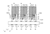
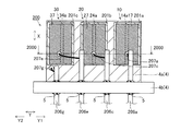
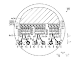
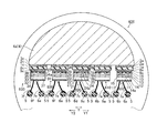
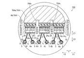
本発明の第1実施形態による半導体レーザ装置100では、図1および図2に示すように、約640nmの発振波長を有する赤色半導体レーザ素子10と、約465nmの発振波長を有する青色半導体レーザ素子20と、約530nmの発振波長を有する緑色半導体レーザ素子30とが、それぞれ、レーザ光の出射方向(X方向)から見て、レーザ光の出射方向と垂直な方向の一方端部側(Y1側)から順に所定の間隔を隔てて配置されている放熱基台1a、1bおよび1c(図2参照)の表面上に接合されている。これにより、半導体レーザ装置100は、RGB3波長半導体レーザ装置を構成している。また、赤色半導体レーザ素子10は、後述するパッケージ4(支持基体4a)のY1側の端部近傍に配置されているとともに、緑色半導体レーザ素子30は、パッケージ4(支持基体4a)のレーザ光の出射方向と垂直な方向の他方端部側(Y2側)の端部近傍に配置されている。なお、赤色半導体レーザ素子10は、約610nm〜約750nmの範囲の発振波長を有するように構成してもよい。また、青色半導体レーザ素子20は、約435nm〜約485nmの範囲の発振波長を有するように構成してもよい。また、緑色半導体レーザ素子30は、約500nm〜約565nmの範囲の発振波長を有するように構成してもよい。なお、放熱基台1aは、本発明の「第1放熱基台」の一例であり、放熱基台1bおよび1cは、それぞれ、本発明の「第2放熱基台」の一例である。
In the
また、半導体レーザ装置100は、ディスプレイ用の光源として使用することが可能なように構成されている。すなわち、半導体レーザ装置100は、ディスプレイ用の光源として使用可能なように、赤色半導体レーザ素子10、青色半導体レーザ素子20および緑色半導体レーザ素子30が、略同時に発振するか、または時系列的にそれぞれ交互に発振するように構成されている。これによって、半導体レーザ装置100を、白色などの複数色を表示可能なディスプレイ用の光源として用いることが可能となるように構成されている。
The
また、第1実施形態では、図2に示すように、放熱基台1a、1bおよび1cは、それぞれ、赤色半導体レーザ素子10、青色半導体レーザ素子20および緑色半導体レーザ素子30において発生した熱を、後述する支持基体4aに放出させるために設けられている。また、放熱基台1a、1bおよび1cは、絶縁性を有するとともに、熱伝導率が大きく熱伝導性が良好なAlNからなる。なお、放熱基台1a、1bおよび1cは、絶縁性を有するとともに、熱伝導率が大きく熱伝導性が良好なダイヤモンドやSiCなどを用いてもよい。さらに、放熱基台1aをCuからなるとともに、放熱基台1bおよび1cをSiからなるように構成してもよい。このように構成すれば、放熱基台1a(Cu)は放熱基台1bおよび1c(Si)に比べて熱伝導率が大きいので、放熱基台1aにおいて赤色半導体レーザ素子10から支持基体4aへの放熱を効率よく行うことができる。また、放熱基台1bおよび1cは放熱基台1aに比べて熱伝導率が小さいので、放熱基台1bおよび1cにおいて緑色半導体レーザ素子30および青色半導体レーザ素子20から支持基体4aへ熱が伝達されるのをある程度遅らせることができる。したがって、赤色半導体レーザ素子10に熱をより伝播させにくくすることができる。
In the first embodiment, as shown in FIG. 2, the
また、放熱基台1a、1bおよび1cは、それぞれ、Auを含む金属層2a、2bおよび2cと、AuSnを含む半田からなる導電性の融着層3a、3bおよび3cとを介して、導電性を有する支持基体4aの平坦面状の面に接合されている。この金属層2a、2bおよび2cは、それぞれ、支持基体4aに対する融着層3a、3bおよび3cの濡れ性を改善するために形成されている。また、支持基体4aは、熱伝導率が大きく熱伝導性が良好なCuまたはFeからなり、表面にはAuメッキが施されている。これにより、支持基体4aは、放熱可能なように構成されている。また、支持基体4aは、導電性を有するステム(支持体)4bに一体的に固定されている。なお、導電性を有する支持基体4aとステム4bとはパッケージ4の構成要素である。また、パッケージ4は、接地されている。
Further, the
ここで、第1実施形態では、赤色半導体レーザ素子10が接合されている放熱基台1aは、支持基体4aのY1側に接合されているとともに、緑色半導体レーザ素子30が接合されている放熱基台1cは、支持基体4aのY2側に接合されている。また、青色半導体レーザ素子20が接合されている放熱基台1bは、放熱基台1aおよび1cの間に配置されるように支持基体4aに接合されている。これにより、赤色半導体レーザ素子10と緑色半導体レーザ素子30とは隣り合わないように青色半導体レーザ素子20を挟んで支持基体4aの表面上に配置されている。さらに、赤色半導体レーザ素子10、青色半導体レーザ素子20および緑色半導体レーザ素子30は、単一のパッケージ4内に配置されているとともに、放熱基台1a、1bおよび1cは、それぞれ、赤色半導体レーザ素子10、青色半導体レーザ素子20および緑色半導体レーザ素子30と支持基体4aとの間に配置されている。
Here, in the first embodiment, the
また、図1および図2に示すように、ステム(支持体)4bには、絶縁リング5を介して、Y1側から順にリード端子6a、6b、6c、6d、6eおよび6fが取り付けられている。このリード端子6a、6b、6c、6d、6eおよび6fは、図示しない電源と接続されている。また、リード端子6a、6b、6c、6d、6eおよび6fには、それぞれ、Auからなる導電性のワイヤ7a、7b、7c、7d、7eおよび7fの一方端が接続されている。このワイヤ7a、7b、7c、7d、7eおよび7fは、半導体レーザ素子(赤色半導体レーザ素子10、青色半導体レーザ素子20および緑色半導体レーザ素子30)に電力を供給するために設けられている。
As shown in FIGS. 1 and 2,
また、図2に示すように、放熱基台1a、1bおよび1cの表面上には、それぞれ、Auを含む金属層8a、8bおよび8cが形成されている。また、図1に示すように、金属層8a、8bおよび8cには、それぞれ、ワイヤ7b、7dおよび7fの他方端が接続されている。
Moreover, as shown in FIG. 2,
また、第1実施形態では、図2に示すように、金属層8a、8bおよび8cの表面上には、それぞれ、導電性を有するとともに、熱伝導率が大きく熱伝導性が良好なAuSnを含む半田からなる融着層9a、9bおよび9cが形成されている。この融着層9a、9bおよび9cは、それぞれ、赤色半導体レーザ素子10、青色半導体レーザ素子20および緑色半導体レーザ素子30を放熱基台1a、1bおよび1c上に接合するために設けられているとともに、赤色半導体レーザ素子10、青色半導体レーザ素子20および緑色半導体レーザ素子30において発生した熱を、放熱基台1a、1bおよび1cに放出させるために設けられている。
In the first embodiment, as shown in FIG. 2, the surfaces of the
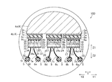
また、第1実施形態では、赤色半導体レーザ素子10は、n型GaAs基板11の表面上に、n型AlGaInPからなるn型クラッド層12、AlInGaPからなる活性層13およびp型AlGaInPからなるp型クラッド層14がこの順番で積層された構造を有している。また、青色半導体レーザ素子20は、n型GaN基板21の表面上に、n型AlInGaNからなるn型クラッド層22、InGaNからなる活性層23およびp型AlInGaNからなるp型クラッド層24がこの順番で積層された構造を有している。また、緑色半導体レーザ素子30は、n型InGaN基板31の表面上に、n型AlInGaNからなるn型クラッド層32、InGaNからなる活性層33およびp型AlInGaNからなるp型クラッド層34がこの順番で積層された構造を有している。また、活性層13、23および33は、単層構造、2層の障壁層(図示せず)と1層の井戸層(図示せず)とが交互に積層された単一量子井戸(SQW)構造、障壁層(図示せず)と井戸層(図示せず)とが交互に複数積層された多重量子井戸(MQW)構造などのいずれの構造により構成されてもよい。
In the first embodiment, the red
また、p型クラッド層14、24および34は、それぞれ、素子の略中央部に形成されたリッジ部14a、24aおよび34aと、リッジ部14a、24aおよび34aのレーザ光の出射方向と垂直な方向(Y方向)に延びる平坦部とを有している。また、図1に示すように、リッジ部14a、24aおよび34aは、それぞれ、共振器方向(X方向)に沿って延びるように形成されている。すなわち、赤色半導体レーザ素子10、青色半導体レーザ素子20および緑色半導体レーザ素子30は、リッジ導波型のレーザ素子構造を有するように構成されている。なお、図2に示すように、リッジ部14a、24aおよび34aを構成するp型クラッド層14、24および34の上部に、それぞれ、後述するp側電極16、26および36とのコンタクト特性を向上させるためのp型コンタクト層を設けてもよい。
The p-type cladding layers 14, 24, and 34 are respectively formed in the
また、第1実施形態では、リッジ部14a、24aおよび34aの下部の活性層13、23および33の部分において、それぞれ、赤色半導体レーザ素子10、青色半導体レーザ素子20および緑色半導体レーザ素子30における本発明の「第1発光部」、「第3発光部」および「第2発光部」がそれぞれ形成されている。また、赤色半導体レーザ素子10、青色半導体レーザ素子20および緑色半導体レーザ素子30は、それぞれ、リッジ部14a、24aおよび34aがパッケージ4の支持基体4a側(Z1側)に位置するように放熱基台1a、1bおよび1cに接合されている。したがって、赤色半導体レーザ素子10、青色半導体レーザ素子20および緑色半導体レーザ素子30は、それぞれ、ジャンクションダウン方式により放熱基台1a、1bおよび1cに接合されている。
Further, in the first embodiment, in the portions of the
また、p型クラッド層14、24および34の平坦部とリッジ部14a、24aおよび34aの側面とを覆うように、SiO2からなる電流ブロック層15、25および35がそれぞれ形成されている。また、リッジ部14a、24aおよび34aと電流ブロック層15、25および35との表面上には、それぞれ、Auなどからなるp側電極16、26および36が形成されている。このp側電極16、26および36は、それぞれ、金属層8a、8bおよび8cと融着層9a、9bおよび9cとを介して、ワイヤ7b、7dおよび7fに接続されている。
Further, current blocking layers 15, 25 and 35 made of SiO 2 are formed so as to cover the flat portions of the p-type cladding layers 14, 24 and 34 and the side surfaces of the
また、n型GaAs基板11の表面上には、Auを含むn側電極17が形成されている。また、n型GaN基板21の表面上には、Auを含むn側電極27が形成されている。また、n型InGaN基板31の表面上には、Auを含むn側電極37が形成されている。また、図1および図2に示すように、n側電極17、27および37には、それぞれ、ワイヤ7a、7cおよび7eの他方端が接続されている。すなわち、パッケージ4(支持基体4a)側とは反対側の電極であるn側電極17、27および37に、それぞれ、1本のワイヤ7a、7cおよび7eが接続されている。
An n-
また、リード端子6aとリード端子6bとの間に電圧(リード端子6bが正電位)を印加することによって、赤色半導体レーザ素子10は、駆動可能なように構成されている。また、リード端子6cとリード端子6dとの間に電圧(リード端子6dが正電位)を印加することによって、青色半導体レーザ素子20は、駆動可能なように構成されている。また、リード端子6eとリード端子6fとの間に電圧(リード端子6fが正電位)を印加することによって、緑色半導体レーザ素子30は、駆動可能なように構成されている。
Further, the red
次に、図2〜図5を参照して、本発明の第1実施形態による半導体レーザ装置100を備えるプロジェクタ装置140および150について説明する。
Next,
まず、図2〜図4を参照して、半導体レーザ素子が時系列的に点灯されるプロジェクタ装置140について説明する。
First, a
本発明の第1実施形態によるプロジェクタ装置140には、図3に示すように、赤色半導体レーザ素子10(図2参照)、青色半導体レーザ素子20(図2参照)および緑色半導体レーザ素子30(図2参照)が設けられた半導体レーザ装置100と、複数の光学部品からなる光学系141と、半導体レーザ装置100および光学系141を制御する制御部142とが設けられている。これにより、半導体レーザ装置100からの光が、光学系141により変調された後、スクリーン143などに投影されるように構成されている。なお、光学系141は、本発明の「変調手段」の一例である。
As shown in FIG. 3, the
また、光学系141において、半導体レーザ装置100から出射された光は、それぞれ、レンズ141aにより平行光に変換された後、ライトパイプ141bに入射される。
In the
ライトパイプ141bは内面が鏡面となっており、光は、ライトパイプ141bの内面で反射を繰り返しながらライトパイプ141b内を進行する。この際、ライトパイプ141b内での多重反射作用によって、ライトパイプ141bから出射される各色の光の強度分布が均一化される。また、ライトパイプ141bから出射された光は、リレー光学系141cを介してデジタルマイクロミラーデバイス(DMD)素子141dに入射される。
The inner surface of the
DMD素子141dは、マトリクス状に配置された微小なミラー群からなる。また、DMD素子141dは、各画素位置の光の反射方向を、投写レンズ141eに向かう第1の方向Aと投写レンズ141eから逸れる第2の方向Bとに切り替えることにより各画素の階調を表現(変調)する機能を有している。各画素位置に入射される光のうち第1の方向Aに反射された光(ON光)は、投写レンズ141eに入射されて被投写面(スクリーン143)に投写される。また、DMD素子141dによって第2の方向Bに反射された光(OFF光)は、投写レンズ141eには入射されずに光吸収体141fによって吸収される。
The
また、プロジェクタ装置140では、制御部142によってパルス電圧が半導体レーザ装置100に供給されるように制御されることによって、半導体レーザ装置100の赤色半導体レーザ素子10、青色半導体レーザ素子20および緑色半導体レーザ素子30は、それぞれ、時系列的に分割されて1素子ずつ交互(cyclic)に駆動されるように構成されている。また、制御部142によって、光学系141のDMD素子141dは、赤色半導体レーザ素子10、青色半導体レーザ素子20および緑色半導体レーザ素子30の駆動とそれぞれ同期しながら、各画素の階調を変調するように構成されている。
Further, in the
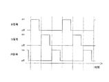
具体的には、図4に示すように、青色半導体レーザ素子20の駆動に関するB信号、緑色半導体レーザ素子30の駆動に関するG信号および赤色半導体レーザ素子10の駆動に関するR信号が、それぞれ互いに重ならないように時系列的に分割され、制御部142によって半導体レーザ装置100の各レーザ素子に供給される。また、このB信号、G信号およびR信号に同期して、制御部142からB画像信号、G画像信号およびR画像信号が、それぞれ、DMD素子141dに出力される。
Specifically, as shown in FIG. 4, the B signal for driving the blue
これにより、B信号に基づいて、青色半導体レーザ素子20の青色光が発光されるとともに、このタイミングで、B画像信号に基づいて、DMD素子141dにより青色光が変調される。また、B信号の次に出力されるG信号に基づいて、緑色半導体レーザ素子30の緑色光が発光されるとともに、このタイミングで、G画像信号に基づいて、DMD素子141dにより緑色光が変調される。さらに、G信号の次に出力されるR信号に基づいて、赤色半導体レーザ素子10の赤色光が発光されるとともに、このタイミングで、R画像信号に基づいて、DMD素子141dにより赤色光が変調される。その後、R信号の次に出力されるB信号に基づいて、青色半導体レーザ素子20の青色光が発光されるとともに、このタイミングで、再度、B画像信号に基づいて、DMD素子141dにより青色光が変調される。上記の動作が繰り返されることによって、B画像信号、G画像信号およびR画像信号に基づいたレーザ光照射による画像が、被投写面(スクリーン143)に投写される。このようにして、本発明の第1実施形態による半導体レーザ装置100が時系列的に交互に点灯されるプロジェクタ装置140が構成されている。
Thereby, the blue light of the blue
次に、図2および図5を参照して、半導体レーザ素子が略同時に点灯されるプロジェクタ装置150について説明する。
Next, a
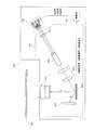
まず、本発明の第1実施形態によるプロジェクタ装置150には、図5に示すように、赤色半導体レーザ素子10(図2参照)、青色半導体レーザ素子20(図2参照)および緑色半導体レーザ素子30(図2参照)が設けられた半導体レーザ装置100と、複数の光学部品からなる光学系151と、半導体レーザ装置100および光学系151を制御する制御部152とが設けられている。これにより、半導体レーザ装置100から出射されたレーザ光が、光学系151により変調された後、外部のスクリーン153などに投影されるように構成されている。なお、光学系151は、本発明の「変調手段」の一例である。
First, as shown in FIG. 5, the
また、光学系151において、半導体レーザ装置100から出射されたレーザ光は、凹レンズと凸レンズとからなる分散角制御レンズ151aにより所定ビーム径を有する平行光に変換された後、フライアイインテグレータ151bに入射される。また、フライアイインテグレータ151bでは、蝿の目状のレンズ群からなる2つのフライアイレンズが向き合うように構成されており、液晶パネル151g、151jおよび151pに入射する際の光量分布が均一となるように分散角制御レンズ151aから入射される光に対してレンズ作用を付与する。すなわち、フライアイインテグレータ151bを透過した光は、液晶パネル151g、151jおよび151pのサイズに対応したアスペクト比(たとえば16:9)の広がりをもって入射できるように調整されている。
In the
また、フライアイインテグレータ151bを透過した光は、コンデンサレンズ151cによって集光される。また、コンデンサレンズ151cを透過した光のうち、赤色光のみがダイクロイックミラー151dによって反射される一方、緑色光および青色光はダイクロイックミラー151dを透過する。
Further, the light transmitted through the
そして、赤色光は、ミラー151eを経てレンズ151fによる平行化の後に液晶パネル151gに入射される。この液晶パネル151gは、赤色用の駆動信号(R画像信号)に応じて駆動されることにより赤色光を変調する。なお、レンズ151fを透過した赤色光は、入射側偏光板(図示せず)を介して液晶パネル151gに入射される。
The red light is incident on the
また、ダイクロイックミラー151hでは、ダイクロイックミラー151dを透過した光のうちの緑色光のみが反射される一方、青色光はダイクロイックミラー151hを透過する。
In the
そして、緑色光は、レンズ151iによる平行化の後に液晶パネル151jに入射される。この液晶パネル151jは、緑色用の駆動信号(G画像信号)に応じて駆動されることにより緑色光を変調する。なお、レンズ151iを透過した緑色光は、入射側偏光板(図示せず)を介して液晶パネル151jに入射される。
The green light is incident on the
また、ダイクロイックミラー151hを透過した青色光は、レンズ151k、ミラー151l、レンズ151mおよびミラー151nを経て、さらにレンズ151oによって平行化がなされた後、液晶パネル151pに入射される。この液晶パネル151pは、青色用の駆動信号(B画像信号)に応じて駆動されることにより青色光を変調する。なお、レンズ151oを透過した青色光は、入射側偏光板(図示せず)を介して液晶パネル151pに入射される。
The blue light transmitted through the
その後、液晶パネル151g、151jおよび151pによって変調された赤色光、緑色光および青色光は、ダイクロイックプリズム151qにより合成された後、出射側偏光板(図示せず)を介して投写レンズ151rへと入射される。また、投写レンズ151rは、投写光を被投写面(スクリーン153)上に結像させるためのレンズ群と、レンズ群の一部を光軸方向に変位させて投写画像のズームおよびフォーカスを調整するためのアクチュエータを内蔵している。
Thereafter, the red light, the green light, and the blue light modulated by the
また、プロジェクタ装置150では、制御部152によって、青色半導体レーザ素子20の駆動に関するB信号、緑色半導体レーザ素子30の駆動に関するG信号および赤色半導体レーザ素子10の駆動に関するR信号としての定常的な電圧が、半導体レーザ装置100各レーザ素子に供給される。これによって、半導体レーザ装置100の赤色半導体レーザ素子10、青色半導体レーザ素子20および緑色半導体レーザ素子30は、それぞれ、実質的に同時に発振されるように構成されている。また、制御部152によって半導体レーザ装置100の赤色半導体レーザ素子10、青色半導体レーザ素子20および緑色半導体レーザ素子30の各々の光の強度を制御することによって、スクリーン153に投写される画素の色相や輝度などが制御されるように構成されている。これにより、制御部152によって所望の画像がスクリーン153に投写される。このようにして、本発明の第1実施形態による半導体レーザ装置100が略同時に点灯されるプロジェクタ装置150が構成されている。
In the
第1実施形態では、上記のように、赤色半導体レーザ素子10と緑色半導体レーザ素子30との間に青色半導体レーザ素子20を支持基体4aの表面上に配置することによって、発熱量の大きい緑色半導体レーザ素子30からの熱が、赤色半導体レーザ素子10に伝播するのを低減することができるので、半導体レーザ装置100の動作時に、赤色半導体レーザ素子10の温度が上昇することに起因する発光特性の劣化を抑制することができる。また、支持基体4aによって、赤色半導体レーザ素子10、青色半導体レーザ素子20および緑色半導体レーザ素子30の各々において発生した熱を外部に放出することができる。
In the first embodiment, as described above, by arranging the blue
また、第1実施形態では、パッケージ4(支持基体4a)側とは反対側の電極であるn側電極17、27および37に、それぞれ、1本のワイヤ7a、7cおよび7eを接続することによって、電力を供給するための配線の自由度を大きくすることができるとともに、各々の半導体レーザ素子(赤色半導体レーザ素子10、青色半導体レーザ素子20および緑色半導体レーザ素子30)に個別に接続されたワイヤ(7a、7cおよび7e)の部分から各々の半導体レーザ素子が発生する熱を放出させることができるので、半導体レーザ装置100の動作時に、赤色半導体レーザ素子10の温度が上昇することに起因する発光特性の劣化を抑制することができる。
Further, in the first embodiment, by connecting one
また、第1実施形態では、赤色半導体レーザ素子10を、n型GaAs基板11上に形成するとともに、緑色半導体レーザ素子30および青色半導体レーザ素子20を、それぞれ、AlInGaNおよびInGaNを含む材料により構成することによって、半導体レーザ装置100における赤色半導体レーザ素子10と、緑色半導体レーザ素子30および青色半導体レーザ素子20とを容易に形成することができる。
In the first embodiment, the red
また、第1実施形態では、放熱基台1aを、放熱基台1bおよび1cから分離することによって、緑色半導体レーザ素子30および青色半導体レーザ素子20からの熱が、放熱基台1a、1bおよび1cを介して、赤色半導体レーザ素子10に伝播するのを低減することができる。また、赤色半導体レーザ素子10において発生する熱を、放熱基台1aから放出させることができるとともに、緑色半導体レーザ素子30および青色半導体レーザ素子20において発生する熱を、それぞれ、放熱基台1cおよび1bから放出させることができる。これらにより、半導体レーザ装置100の動作時に、赤色半導体レーザ素子10の温度が上昇することに起因する発光特性の劣化をより抑制することができる。また、緑色半導体レーザ素子30において発生する熱および青色半導体レーザ素子20において発生する熱を、放熱基台1cおよび1bにおいて別々に放出させることができるので、赤色半導体レーザ素子10に熱をさらに伝播させにくくすることができる。
In the first embodiment, the
また、第1実施形態では、赤色半導体レーザ素子10のリッジ部14aを、支持基体4a側に形成することによって、赤色半導体レーザ素子10の発光部(リッジ部14aの下部の活性層13の部分)において発生する熱を、容易に、赤色半導体レーザ素子10の発光部の近傍に設けられた支持基体4aから放出させることができるので、半導体レーザ装置100の動作時に、赤色半導体レーザ素子10の温度が上昇することに起因する発光特性の劣化をより抑制することができる。
In the first embodiment, the
また、第1実施形態では、赤色半導体レーザ素子10、緑色半導体レーザ素子30および青色半導体レーザ素子20を、略同時に発振するか、または時系列的に交互に発振するように構成することによって、赤色半導体レーザ素子10、緑色半導体レーザ素子30および青色半導体レーザ素子20を駆動させることにより発生する熱量が大きくなる状態において、赤色半導体レーザ素子10と緑色半導体レーザ素子30とを隣り合わないように配置することにより、発熱量の大きい緑色半導体レーザ素子30からの熱が、赤色半導体レーザ素子10に伝播するのを低減することができるので、半導体レーザ装置100の動作時に、赤色半導体レーザ素子10の温度が上昇することに起因する発光特性の劣化を有効に抑制することができる。
In the first embodiment, the red
また、第1実施形態では、赤色半導体レーザ素子10、青色半導体レーザ素子20および緑色半導体レーザ素子30を、それぞれ、ジャンクションダウン方式により放熱基台1a、1bおよび1c(支持基体4a側)に接合することによって、赤色半導体レーザ素子10の第1発光部において発生する熱を、第1発光部の近傍に位置する放熱基台1aおよび支持基体4aから容易に放出させることができる。さらに、緑色半導体レーザ素子30の第2発光部において発生する熱と、青色半導体レーザ素子20の第3発光部において発生する熱とを、第3発光部および第2発光部の近傍に位置する放熱基台1cおよび1bと支持基体4aとから容易に放出させることができる。
In the first embodiment, the red
また、第1実施形態では、赤色半導体レーザ素子10を支持基体4aのY1側の端部近傍に配置し、かつ、緑色半導体レーザ素子30を支持基体4aのY2側の端部近傍に配置することによって、赤色半導体レーザ素子10と緑色半導体レーザ素子30との間隔を大きくすることができるので、発熱量の大きい緑色半導体レーザ素子30からの熱が、赤色半導体レーザ素子10に伝播するのをより低減することができるとともに、赤色半導体レーザ素子10の温度が上昇することに起因する発光特性の劣化をより抑制することができる。
In the first embodiment, the red
また、第1実施形態では、プロジェクタ装置140において、制御部142によってパルス電圧を半導体レーザ装置100に供給するように制御することにより、半導体レーザ装置100の赤色半導体レーザ素子10、青色半導体レーザ素子20および緑色半導体レーザ素子30を、それぞれ、時系列的に分割されて1素子ずつ交互に駆動(発振)するように構成されている。この場合、赤色半導体レーザ素子10、青色半導体レーザ素子20および緑色半導体レーザ素子30を駆動させることにより発生する熱量は、時系列的に分割されて1素子ずつ交互に駆動されることに起因して、赤色半導体レーザ素子10のみを駆動させた場合と比べて大きくなるが、このような場合においても、赤色半導体レーザ素子10と緑色半導体レーザ素子30とを隣り合わないように配置することにより、発熱量の大きい緑色半導体レーザ素子30からの熱が、赤色半導体レーザ素子10に伝播するのを低減することができるので、半導体レーザ装置100の動作時に、赤色半導体レーザ素子10の温度が上昇することに起因する発光特性の劣化を有効に抑制することができる。
In the first embodiment, in the
また、第1実施形態では、プロジェクタ装置150において、制御部152によって定常的な電圧を半導体レーザ装置100に供給するように制御することにより、半導体レーザ装置100の赤色半導体レーザ素子10、青色半導体レーザ素子20および緑色半導体レーザ素子30を、それぞれ、実質的に同時に発振するように構成されている。この場合、赤色半導体レーザ素子10、青色半導体レーザ素子20および緑色半導体レーザ素子30を駆動させることにより発生する熱量は、各々の半導体レーザ素子が実質的に同時に発振されることに起因して、赤色半導体レーザ素子10のみを駆動させた場合と比べて大きくなるが、このような場合においても、赤色半導体レーザ素子10と緑色半導体レーザ素子30とを隣り合わないように配置することにより、発熱量の大きい緑色半導体レーザ素子30からの熱が、赤色半導体レーザ素子10に伝播するのを低減することができるので、半導体レーザ装置100の動作時に、赤色半導体レーザ素子10の温度が上昇することに起因する発光特性の劣化を有効に抑制することができる。
In the first embodiment, the
また、第1実施形態では、プロジェクタ装置140に、半導体レーザ装置100と光学系141とを設けるとともに、プロジェクタ装置150に、半導体レーザ装置100と光学系151とを設けることによって、発振波長の長い赤色半導体レーザ素子10が劣化するのを抑制することができる半導体レーザ装置100を用いて、光学系141および151により光を変調させて所望の画像を表示させることができる。
In the first embodiment, the
(第1実施形態の変形例)
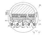
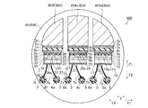
次に、図1、図6および図7を参照して第1実施形態の変形例について説明する。この第1実施形態の変形例による半導体レーザ装置200では、上記第1実施形態と異なり、p側電極16、26および36が、導電性を有する放熱基台201a、201bおよび201cを介して、支持基体4aと電気的に接続されることにより、正極(p側)が共通のアノードコモン結線が実現されている場合について説明する。
(Modification of the first embodiment)
Next, a modification of the first embodiment will be described with reference to FIG. 1, FIG. 6, and FIG. In the
本発明の第1実施形態の変形例による半導体レーザ装置200では、図6および図7に示すように、接地されているパッケージ4の導電性を有するステム(支持体)4bには、Y1側から順にリード端子206a、206c、206eおよび206gが取り付けられている。また、リード端子206a、206c、206eおよび206gには、それぞれ、ワイヤ207a、207c、207eおよび207gの一方端が接続されている。また、図6に示すように、ワイヤ207gの他方端は、導電性を有する支持基体4aの表面上に接続されている。
In the
ここで、第1実施形態の変形例では、図7に示すように、赤色半導体レーザ素子10、青色半導体レーザ素子20および緑色半導体レーザ素子30は、それぞれ、融着層9a、9bおよび9cによって、Y1側から順に所定の間隔を隔てて配置されている放熱基台201a、201bおよび201cに接合されている。この放熱基台201a、201bおよび201cは、導電性を有するとともに、熱伝導率が大きく熱伝導性が良好なCuからなる。なお、放熱基台201a、201bおよび201cは、導電性を有するとともに、熱伝導率が大きく熱伝導性が良好なAlなどを用いてもよい。なお、放熱基台201aは、本発明の「第1放熱基台」の一例であり、放熱基台201bおよび201cは、それぞれ、本発明の「第2放熱基台」の一例である。
Here, in the modification of the first embodiment, as shown in FIG. 7, the red
また、第1実施形態の変形例では、放熱基台201a、201bおよび201cは、それぞれ、AuSnを含む半田からなる導電性の融着層3a、3bおよび3cを介して、導電性の支持基体4aに接合されている。これにより、赤色半導体レーザ素子10のp側電極16、青色半導体レーザ素子20のp側電極26および緑色半導体レーザ素子30のp側電極36は、それぞれ、融着層9a、9bおよび9cと、放熱基台201a、201bおよび201cと、融着層3a、3bおよび3cとを介して、支持基体4aと電気的に接続されている。すなわち、赤色半導体レーザ素子10のp側電極16と、青色半導体レーザ素子20のp側電極26と、緑色半導体レーザ素子30のp側電極36とがすべて接続された、正極(p側)が共通であるアノードコモン結線が実現されている。これにより、上記第1実施形態における3本のリード端子6b、6dおよび6f(図1参照)が、リード端子206gに一本化されるとともに、第1実施形態における3本のワイヤ7b、7dおよび7f(図1参照)が、ワイヤ207gに一本化される。この結果、リード端子およびワイヤの本数を削減することが可能であるので、ワイヤ配線を簡略化することが可能であるとともに、半導体レーザ装置200を小型化することが可能である。
In the modification of the first embodiment, the
また、図6および図7に示すように、n側電極17、27および37には、それぞれ、ワイヤ207a、207cおよび207eの他方端が接続されている。これにより、リード端子206aとリード端子206gとの間に電圧を印加することによって、赤色半導体レーザ素子10は、駆動可能なように構成されている。また、リード端子206cとリード端子206gとの間に電圧を印加することによって、青色半導体レーザ素子20は、駆動可能なように構成されている。また、リード端子206eとリード端子206gとの間に電圧を印加することによって、緑色半導体レーザ素子30は、駆動可能なように構成されている。なお、第1実施形態の変形例のその他の構造は、上記第1実施形態と同様である。
Further, as shown in FIGS. 6 and 7, the other ends of the
第1実施形態の変形例では、上記のように、パッケージ4(支持基体4a)、放熱基台201a、201bおよび201cが、それぞれ、導電性を有するように構成することによって、パッケージ4と、赤色半導体レーザ素子10のp側電極16、緑色半導体レーザ素子30のp側電極36および青色半導体レーザ素子20のp側電極26とを接続するためのワイヤが不要になるので、半導体レーザ装置200におけるワイヤ配線が複雑化するのを抑制することができる。なお、第1実施形態の変形例の効果は、上記第1実施形態と同様である。
In the modification of the first embodiment, as described above, the package 4 (
(第2実施形態)
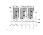
次に、図8および図9を参照して第2実施形態について説明する。この第2実施形態による半導体レーザ装置300では、上記第1実施形態と異なり、青色半導体レーザ素子20と緑色半導体レーザ素子30とが、同一の放熱基台301dの表面上に所定の間隔を隔てて接合されている場合について説明する。なお、放熱基台301dは、本発明の「第2放熱基台」の一例である。
(Second Embodiment)
Next, a second embodiment will be described with reference to FIGS. 8 and 9. In the
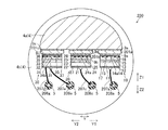
本発明の第2実施形態による半導体レーザ装置300では、図8および図9に示すように、青色半導体レーザ素子20と緑色半導体レーザ素子30とが、放熱基台301dの表面上に所定の間隔を隔てて接合されている。具体的には、図9に示すように、絶縁性を有するとともに、熱伝導率が大きく熱伝導性が良好なAlNからなる放熱基台301dは、支持基体4aのY2側から中央部近傍までY方向に延びるように配置されている。また、放熱基台301dは、AuSnを含む半田からなる導電性の融着層303dによって、Auを含む金属層302dを介して、導電性を有する支持基体4aのY2側に接合されている。
In the
また、青色半導体レーザ素子20のp側電極26側は、融着層9bによって、放熱基台301dのY1側の金属層8bの上にジャンクションダウン方式で接合されている。また、緑色半導体レーザ素子30のp側電極36側は、融着層9cによって、放熱基台301dのY2側の金属層8cの上にジャンクションダウン方式で接合されている。また、第1実施形態と同様に、赤色半導体レーザ素子10は、融着層9aによって、支持基体4aのY1側に接合された放熱基台1aに金属層8aを介して接合されている。これにより、赤色半導体レーザ素子10と緑色半導体レーザ素子30とは隣り合わないように青色半導体レーザ素子20を挟んで配置されている。なお、第2実施形態のその他の構造は、上記第1実施形態と同様である。
Further, the p-
第2実施形態では、上記のように、青色半導体レーザ素子20と緑色半導体レーザ素子30とを、同一の放熱基台301dの表面上に間隔を隔てて接合することによって、半導体レーザ装置300の組立時に、使用部品点数を減らすことができるので、容易に、半導体レーザ装置300を組み立てることができる。なお、第2実施形態のその他の効果は、上記第1実施形態と同様である。
In the second embodiment, as described above, the blue
(第3実施形態)
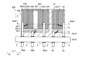
次に、図10および図11を参照して第3実施形態について説明する。この第3実施形態による半導体レーザ装置400では、上記第2実施形態と異なり、青色半導体レーザ素子420および緑色半導体レーザ素子430により、モノリシック型の青・緑2波長半導体レーザ素子部460を形成している場合について説明する。
(Third embodiment)
Next, a third embodiment will be described with reference to FIGS. 10 and 11. In the
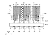
本発明の第3実施形態による半導体レーザ装置400では、図10に示すように、パッケージ4のステム(支持体)4bには、Y1側から順にリード端子6a、6b、406d、406hおよび406fが取り付けられている。また、リード端子6a、6b、406d、406hおよび406fには、それぞれ、ワイヤ7a、7b、407d、407hおよび407fの一方端が接続されている。
In the
ここで、第3実施形態では、図11に示すように、青色半導体レーザ素子420および緑色半導体レーザ素子430は、モノリシック型の青・緑2波長半導体レーザ素子部460を形成している。具体的には、青色半導体レーザ素子420は、n型GaN基板461のY1側の表面上に、n型AlInGaNからなるn型クラッド層422と、InGaNからなる活性層423と、リッジ部424aを有するp型AlInGaNからなるp型クラッド層424とがこの順番で積層された構造を有している。また、緑色半導体レーザ素子430は、青色半導体レーザ素子420が形成された基板と同一のn型GaN基板461のY2側の表面上に、n型AlInGaNからなるn型クラッド層432と、InGaNからなる活性層433と、リッジ部434aを有するp型AlInGaNからなるp型クラッド層434とがこの順番で積層された構造を有している。また、リッジ部424aおよび434aの下部の活性層423および433の部分において、それぞれ、青色半導体レーザ素子420および緑色半導体レーザ素子430における本発明の「第2発光部」および「第3発光部」がそれぞれ形成されている。
Here, in the third embodiment, as shown in FIG. 11, the blue
また、p型クラッド層424および434の平坦部とリッジ部424aおよび434aの側面とを覆うように、SiO2からなる電流ブロック層425および435がそれぞれ形成されている。また、リッジ部424aおよび434aと電流ブロック層425および435との表面上には、それぞれ、Auなどからなるp側電極426および436が形成されている。なお、リッジ部424aおよび434aを構成するp型クラッド層424および434の上部に、それぞれ、p側電極426および436とのコンタクト特性を向上させるためのp型コンタクト層を設けてもよい。また、n型GaN基板461の表面上には、Auを含むn側電極462が形成されている。これにより、青色半導体レーザ素子420のn側電極462と緑色半導体レーザ素子430のn側電極462とが接続された、負極(n側)が共通であるカソードコモン結線が実現されている。
Current blocking layers 425 and 435 made of SiO 2 are formed so as to cover the flat portions of the p-type cladding layers 424 and 434 and the side surfaces of the
また、青色半導体レーザ素子420のp側電極426は、融着層9bによって、放熱基台301dのY1側の金属層8bの上にジャンクションダウン方式で接合されている。また、緑色半導体レーザ素子430のp側電極436は、融着層9cによって、放熱基台301dのY2側の金属層8cの上にジャンクションダウン方式で接合されている。また、図10に示すように、金属層8bおよび8cには、それぞれ、ワイヤ407dおよび407fの他方端が接続されている。また、図10および図11に示すように、n側電極462には、ワイヤ407hの他方端が接続されている。
Further, the p-
また、上記第2実施形態(第1実施形態)と同様に、リード端子6aとリード端子6bとの間に電圧(リード端子6bが正電位)を印加することによって、赤色半導体レーザ素子10は、駆動可能なように構成されている。また、リード端子406hとリード端子406dとの間に電圧(リード端子406dが正電位)を印加することによって、青色半導体レーザ素子420は、駆動可能なように構成されている。また、リード端子406hとリード端子406fとの間に電圧(リード端子406fが正電位)を印加することによって、緑色半導体レーザ素子430は、駆動可能なように構成されている。なお、第3実施形態のその他の構造は、上記第2実施形態と同様である。
Similarly to the second embodiment (first embodiment), by applying a voltage (lead terminal 6b is positive potential) between the
第3実施形態では、上記のように、青色半導体レーザ素子420および緑色半導体レーザ素子430を、モノリシック型の青・緑2波長半導体レーザ素子部460として形成することによって、青色半導体レーザ素子420および緑色半導体レーザ素子430のn側電極462に対して、共通のリード端子406hおよびワイヤ407hを使用することができるので、リード端子およびワイヤの数を減少させることができる。さらに、ワイヤの本数が少なくて済むので、ワイヤ配線を簡略化することができる。
In the third embodiment, as described above, the blue
また、第3実施形態では、青色半導体レーザ素子420および緑色半導体レーザ素子430を、モノリシック型の青・緑2波長半導体レーザ素子部460として形成することによって、青色半導体レーザ素子420の発光点と緑色半導体レーザ素子430の発光点とのY方向の間隔がより正確に位置決めした状態で、青・緑2波長半導体レーザ素子部460を放熱基台301dの表面上に接合することができる。
In the third embodiment, the blue
また、第3実施形態では、緑色半導体レーザ素子430および青色半導体レーザ素子420が、共通のn側電極462を有するように構成することによって、緑色半導体レーザ素子430のn側電極462および青色半導体レーザ素子420のn側電極462に共通の電源を接続して、緑色半導体レーザ素子430および青色半導体レーザ素子420を駆動させることができる。なお、第3実施形態のその他の効果は、上記第2実施形態と同様である。
In the third embodiment, the green
(第4実施形態)
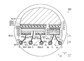
次に、図12および図13を参照して第4実施形態について説明する。この第4実施形態による半導体レーザ装置500では、上記第3実施形態と異なり、モノリシック型の青・緑2波長半導体レーザ素子部460を構成している青色半導体レーザ素子420と緑色半導体レーザ素子430とが、放熱基台301dにジャンクションアップ方式で接合されている場合について説明する。
(Fourth embodiment)
Next, a fourth embodiment will be described with reference to FIGS. In the
本発明の第4実施形態による半導体レーザ装置500では、図12に示すように、パッケージ4のステム(支持体)4bには、Y1側から順にリード端子6a、6b、506d、506iおよび506fが取り付けられている。また、リード端子6a、6b、506d、506iおよび506fには、それぞれ、ワイヤ7a、7b、507d、507iおよび507fの一方端が接続されている。
In the
ここで、第4実施形態では、図13に示すように、モノリシック型の青・緑2波長半導体レーザ素子部460を構成している青色半導体レーザ素子420と緑色半導体レーザ素子430とが、放熱基台301dにジャンクションアップ方式で接合されている。具体的には、青色半導体レーザ素子420のp側電極426および緑色半導体レーザ素子430のp側電極436が支持基体4a側とは反対側(Z2側)に位置するように、青色半導体レーザ素子420と緑色半導体レーザ素子430との共通のn側電極462が、融着層509dを介して、放熱基台301dの表面上に形成された金属層508dに接合されている。これにより、青色半導体レーザ素子420および緑色半導体レーザ素子430は、それぞれ、リッジ部424aおよび434aが放熱基台301dとは反対側(Z2側)に位置するように放熱基台301dに接合されている。また、p側電極426および436には、それぞれ、ワイヤ507dおよび507fの他方端が接続されている。また、図12に示すように、金属層508dには、ワイヤ507iの他方端が接続されている。
Here, in the fourth embodiment, as shown in FIG. 13, the blue
また、リード端子506dとリード端子506iとの間に電圧を印加することによって、青色半導体レーザ素子420は、駆動可能なように構成されている。また、リード端子506fとリード端子506iとの間に電圧を印加することによって、緑色半導体レーザ素子430は、駆動可能なように構成されている。なお、第4実施形態のその他の構造は、上記第3実施形態と同様である。
Further, the blue
第4実施形態では、上記のように、青・緑2波長半導体レーザ素子部460を構成する青色半導体レーザ素子420と緑色半導体レーザ素子430とを、放熱基台301dにジャンクションアップ方式で接合することによって、ジャンクションダウン方式で接合する場合と比べて、青色半導体レーザ素子420の第3発光部(リッジ部424aの下部の活性層423の部分)と緑色半導体レーザ素子430の第2発光部(リッジ部434aの下部の活性層433の部分)とを放熱基台301dからZ2方向に遠ざけることができるので、青色半導体レーザ素子420の第3発光部および緑色半導体レーザ素子430の第2発光部において発生した熱が、放熱基台301d、パッケージ4および放熱基台1aを介して、赤色半導体レーザ素子10に伝播するのを低減することができる。これにより、赤色半導体レーザ素子10の温度が上昇することに起因する発光特性の劣化をより抑制することができる。なお、第4実施形態のその他の効果は、上記第3実施形態と同様である。
In the fourth embodiment, as described above, the blue
なお、今回開示された実施形態は、すべての点で例示であって制限的なものではないと考えられるべきである。本発明の範囲は、上記した実施形態の説明ではなく特許請求の範囲によって示され、さらに特許請求の範囲と均等の意味および範囲内でのすべての変更が含まれる。 The embodiment disclosed this time should be considered as illustrative in all points and not restrictive. The scope of the present invention is shown not by the above description of the embodiments but by the scope of claims for patent, and further includes all modifications within the meaning and scope equivalent to the scope of claims for patent.
たとえば、上記第1〜第4実施形態では、半導体レーザ装置が、赤色半導体レーザ素子と、青色半導体レーザ素子と、緑色半導体レーザ素子とをそれぞれ1つずつ備えた例について示したが、本発明はこれに限られない。本発明では、半導体レーザ装置を、4つ以上の半導体レーザ素子を備えるように構成してもよい。この際、赤色半導体レーザ素子と緑色半導体レーザ素子とは隣り合わないように配置する必要がある。たとえば、図14の半導体レーザ装置600のように、単一のパッケージ4の支持基体4a上に、Y1側から順に、赤色半導体レーザ素子610、赤色半導体レーザ素子610、青色半導体レーザ素子620、緑色半導体レーザ素子630、緑色半導体レーザ素子630と並ぶように配置することによって、赤色半導体レーザ素子610と緑色半導体レーザ素子630とが隣り合わないように配置してもよい。これにより、発熱量の大きい緑色半導体レーザ素子630からの熱が緑色半導体レーザ素子630と隣り合わないように複数配置された赤色半導体レーザ素子610の各々に伝播するのを低減することができるので、半導体レーザ装置600の動作時に、各々の赤色半導体レーザ素子610の温度が上昇することに起因する発光特性の劣化を抑制することができる。
For example, in the first to fourth embodiments, the semiconductor laser device has been described as an example in which each of the semiconductor laser device includes one red semiconductor laser element, one blue semiconductor laser element, and one green semiconductor laser element. It is not limited to this. In the present invention, the semiconductor laser device may be configured to include four or more semiconductor laser elements. At this time, it is necessary to arrange the red semiconductor laser element and the green semiconductor laser element so as not to be adjacent to each other. For example, as in the
また、上記第1〜第4実施形態では、パッケージの支持基体の放熱基台側の面を平坦面状に形成した例について示したが、本発明はこれに限られない。たとえば、図15の半導体レーザ装置700のように、パッケージ704の支持基体704aの放熱基台1a、1bおよび1c側の面で、かつ、放熱基台1aと1bとの間および放熱基台1bと1cの間に、それぞれ、溝部704cを設けてもよい。これにより、支持基体704aの溝部704cによって、緑色半導体レーザ素子30および青色半導体レーザ素子20からの熱が赤色半導体レーザ素子10に伝播するのを一層低減することができる。
Moreover, although the said 1st-4th embodiment showed about the example which formed the surface by the side of the thermal radiation base of the support base | substrate of a package in flat surface shape, this invention is not limited to this. For example, as in the
また、上記第1〜第4実施形態では、パッケージの支持基体の放熱基台側の面を平坦面状に形成した例について示したが、本発明はこれに限られない。たとえば、図16の半導体レーザ装置800のように、パッケージ804の支持基体を放熱基台1a、1bおよび1cごとに、それぞれ、支持基体804d、804eおよび804fに分離させるように構成してもよい。なお、支持基体804dは、本発明の「第1支持基体」の一例であり、支持基体804eおよび804fは、それぞれ、本発明の「第2支持基体」の一例である。これにより、放熱基台1a、1bおよび1cがそれぞれ分離されているのみならず、放熱基台1aが配置される支持基体804dと、放熱基台1bが配置される支持基体804eと、放熱基台1cが配置される支持基体804fともそれぞれ分離されているので、緑色半導体レーザ素子30および青色半導体レーザ素子20からの熱が赤色半導体レーザ素子10に伝播するのをより一層低減することができる。
Moreover, although the said 1st-4th embodiment showed about the example which formed the surface by the side of the thermal radiation base of the support base | substrate of a package in flat surface shape, this invention is not limited to this. For example, like the
また、上記第1〜第4実施形態では、支持基体側とは反対側の電極に、それぞれ1本のワイヤを接続した例を示したが、本発明はこれに限られない。たとえば、図17の半導体レーザ装置900のように、図1の第1実施形態におけるレーザ装置100のn側電極17、27および37に、それぞれ、ワイヤ7a、7cおよび7eを接続するとともに、ワイヤ907j、907kおよび907lの一方端をそれぞれ接続することによって、n側電極17、27および37にそれぞれ2本のワイヤを接続してもよい。これにより、各々の半導体レーザ素子に複数個ワイヤを接続することによって、各々の半導体レーザ素子からより放熱させることが可能である。なお、ワイヤ907j、907kおよび907lの他方端は、それぞれ、リード端子6a、6cおよび6eに接続されている。また、各々の半導体レーザ素子の支持基体側とは反対側の電極に、それぞれ、3本以上のワイヤを接続してもよい。
Moreover, although the said 1st-4th embodiment showed the example which connected one wire to the electrode on the opposite side to the support base | substrate side, this invention is not limited to this. For example, like the
また、上記第1〜第4実施形態では、青色半導体レーザ素子および緑色半導体レーザ素子を、成長用基板(n型GaN基板およびn型InGaN基板)を有する状態で放熱基台に接合した例を示したが、本発明はこれに限られない。本発明では、Geなどからなる支持基板に貼り替えて成長用基板を除去した後に、青色半導体レーザ素子および緑色半導体レーザ素子を放熱基台に接合してもよい。 Moreover, in the said 1st-4th embodiment, the example which joined the blue semiconductor laser element and the green semiconductor laser element to the thermal radiation base in the state which has a growth substrate (n type GaN substrate and n type InGaN substrate) is shown. However, the present invention is not limited to this. In the present invention, the blue semiconductor laser element and the green semiconductor laser element may be bonded to the heat dissipation base after being attached to a support substrate made of Ge or the like and removing the growth substrate.
また、上記第1〜第4実施形態(第1実施形態の変形例を除く)では、導電性を有する支持基体およびステム(支持体)によってパッケージを構成した例について示したが、本発明はこれに限られない。本発明では、支持基体およびステムを、セラミックスなどの熱伝導率が大きく熱伝導性の良好な絶縁体からなるように構成してもよい。 In the first to fourth embodiments (except for the modification of the first embodiment), an example in which a package is configured by a conductive support base and a stem (support) is shown. Not limited to. In the present invention, the support base and the stem may be configured to be made of an insulator having a high thermal conductivity such as ceramics and a good thermal conductivity.
また、上記第1〜第4実施形態では、青色半導体レーザ素子および緑色半導体レーザ素子を、AlInGaNやInGaNなどの窒化物系半導体層により形成した例について示したが、本発明はこれに限られない。本発明では、青色半導体レーザ素子および緑色半導体レーザ素子を、AlN、InN、BN、TlNおよびこれらの混晶からなるウルツ鉱構造の窒化物系半導体層により形成してもよい。 In the first to fourth embodiments, the blue semiconductor laser element and the green semiconductor laser element are shown as being formed of nitride semiconductor layers such as AlInGaN and InGaN. However, the present invention is not limited to this. . In the present invention, the blue semiconductor laser element and the green semiconductor laser element may be formed of a nitride semiconductor layer having a wurtzite structure made of AlN, InN, BN, TlN, and mixed crystals thereof.
また、上記第1〜第4実施形態では、赤色半導体レーザ素子が接合される放熱基台と、青色半導体レーザ素子および緑色半導体レーザ素子が接合される放熱基台とを異ならせた例を示したが、本発明はこれに限られない。本発明では、赤色半導体レーザ素子が接合される放熱基台と、青色半導体レーザ素子および緑色半導体レーザ素子が接合される放熱基台とが共通であってもよい。 Moreover, in the said 1st-4th embodiment, the example which varied the heat dissipation base to which a red semiconductor laser element was joined and the heat dissipation base to which a blue semiconductor laser element and a green semiconductor laser element were joined was shown. However, the present invention is not limited to this. In the present invention, the heat dissipation base to which the red semiconductor laser element is bonded and the heat dissipation base to which the blue semiconductor laser element and the green semiconductor laser element are bonded may be common.
また、上記第1〜第4実施形態では、赤色半導体レーザ素子を、ジャンクションダウン方式で放熱基台に接合した例を示したが、本発明はこれに限られない。本発明では、赤色半導体レーザ素子を、ジャンクションアップ方式で放熱基台に接合してもよい。 Moreover, in the said 1st-4th embodiment, although the example which joined the red semiconductor laser element to the thermal radiation base by the junction down system was shown, this invention is not limited to this. In the present invention, the red semiconductor laser element may be joined to the heat dissipation base by a junction-up method.
また、上記第4実施形態では、モノリシック型の青・緑2波長半導体レーザ素子部460を構成している青色半導体レーザ素子420および緑色半導体レーザ素子430を、ジャンクションアップ方式で放熱基台に接合した例を示したが、本発明はこれに限られない。本発明では、個々の青色半導体レーザ素子および緑色半導体レーザ素子を、それぞれ、ジャンクションアップ方式で放熱基台に接合してもよい。また、青色半導体レーザ素子および緑色半導体レーザ素子のいずれか一方をジャンクションアップ方式で放熱基台に接合し、他方をジャンクションダウン方式で放熱基台に接合してもよい。この場合、赤色半導体レーザ素子へ伝播する熱の影響を考えて、緑色半導体レーザ素子をジャンクションアップ方式で放熱基台に接合する方が好ましい。
In the fourth embodiment, the blue
また、上記第3実施形態では、青色半導体レーザ素子420および緑色半導体レーザ素子430を、1つの放熱基台301dの表面上に接合した例について示したが、本発明はこれに限られない。本発明では、青色半導体レーザ素子および緑色半導体レーザ素子を、それぞれ、2つの放熱基台の表面上に個別に接合してもよい。
In the third embodiment, an example in which the blue
また、上記第1〜第4実施形態では、赤色半導体レーザ素子および緑色半導体レーザ素子をそれぞれ支持基体の端部近傍に接着した例について示したが、本発明はこれに限られない。本発明では、赤色半導体レーザ素子および緑色半導体レーザ素子を支持基体の中央近傍に接着してもよい。この際、赤色半導体レーザ素子と緑色半導体レーザ素子とが互いに隣り合わないように、赤色半導体レーザ素子と緑色半導体レーザ素子との間に青色半導体レーザ素子が配置されている必要がある。 In the first to fourth embodiments, the example in which the red semiconductor laser element and the green semiconductor laser element are bonded to the vicinity of the end of the support base has been described. However, the present invention is not limited to this. In the present invention, the red semiconductor laser element and the green semiconductor laser element may be bonded near the center of the support base. At this time, the blue semiconductor laser element needs to be disposed between the red semiconductor laser element and the green semiconductor laser element so that the red semiconductor laser element and the green semiconductor laser element are not adjacent to each other.
また、上記第1実施形態では、プロジェクタ装置が液晶パネルを有する光学系を備える場合およびDMD素子を有する光学系を備える場合を示したが、本発明はこれに限られない。本発明では、プロジェクタ装置は変調手段を備えるものであればよく、たとえば、プロジェクタ装置がスキャンミラーを有する光学系を備えるように構成してもよい。 Moreover, although the case where the projector apparatus includes an optical system including a liquid crystal panel and the optical system including a DMD element have been described in the first embodiment, the present invention is not limited thereto. In the present invention, the projector device only needs to have a modulation unit, and for example, the projector device may be configured to include an optical system having a scan mirror.
1a、201a 放熱基台(第1放熱基台)
1b、1c、201b、201c、301d 放熱基台(第2放熱基台)
4、704、804 パッケージ
4a、704a 支持基体
7a、7b、7c、7d、7e、7f、207g、407h、507i、907j、907k、907l ワイヤ
10、610 赤色半導体レーザ素子
20、420、620 青色半導体レーザ素子
30、430、630 緑色半導体レーザ素子
100、200、300、400、500、600、700、800、900 半導体レーザ装置
140、150 プロジェクタ装置
141、151 光学系(変調手段)
704c 溝部
804d 支持基体(第1支持基体)
804e、804f 支持基体(第2支持基体)
X 出射方向
1a, 201a Heat radiation base (first heat radiation base)
1b, 1c, 201b, 201c, 301d Heat radiation base (second heat radiation base)
4, 704, 804
804e, 804f Support base (second support base)
X Outgoing direction
Claims (8)
緑色半導体レーザ素子と、
青色半導体レーザ素子とを備え、
前記赤色半導体レーザ素子、前記緑色半導体レーザ素子および前記青色半導体レーザ素子の各々が電力を供給するためのワイヤに個別に接続された状態で単一のパッケージ内に配置され、かつ、レーザ光の出射方向から見て、前記赤色半導体レーザ素子と前記緑色半導体レーザ素子との間に前記青色半導体レーザ素子が配置されている、半導体レーザ装置。 A red semiconductor laser element;
A green semiconductor laser element;
A blue semiconductor laser element,
Each of the red semiconductor laser element, the green semiconductor laser element, and the blue semiconductor laser element is disposed in a single package in a state of being individually connected to a wire for supplying power, and emitting laser light A semiconductor laser device, wherein the blue semiconductor laser element is disposed between the red semiconductor laser element and the green semiconductor laser element when viewed from the direction.
第2発光部を有する緑色半導体レーザ素子と、
第3発光部を有する青色半導体レーザ素子と、
前記赤色半導体レーザ素子、前記緑色半導体レーザ素子および前記青色半導体レーザ素子が配置された支持基体を有するパッケージとを備え、
レーザ光の出射方向から見て、前記赤色半導体レーザ素子と前記緑色半導体レーザ素子との間に前記青色半導体レーザ素子が配置され、前記第1発光部、前記第2発光部および前記第3発光部がそれぞれ前記支持基体側になるように配置されている、半導体レーザ装置。 A red semiconductor laser element having a first light emitting portion;
A green semiconductor laser element having a second light emitting portion;
A blue semiconductor laser element having a third light emitting portion;
A package having a support substrate on which the red semiconductor laser element, the green semiconductor laser element, and the blue semiconductor laser element are disposed;
The blue semiconductor laser element is disposed between the red semiconductor laser element and the green semiconductor laser element when viewed from the direction of laser light emission, and the first light emitting part, the second light emitting part, and the third light emitting part Is a semiconductor laser device arranged so as to be on the side of the support base.
前記緑色半導体レーザ素子および前記青色半導体レーザ素子と前記支持基体との間に配置される少なくとも1つの第2放熱基台とをさらに備え、
前記第1放熱基台は、前記第2放熱基台から分離されている、請求項2または3に記載の半導体レーザ装置。 A first heat dissipation base disposed between the red semiconductor laser element and the support base;
And further comprising at least one second heat dissipation base disposed between the green semiconductor laser element and the blue semiconductor laser element and the support base,
4. The semiconductor laser device according to claim 2, wherein the first heat radiation base is separated from the second heat radiation base. 5.
前記半導体レーザ装置からの光の変調を行う変調手段とを備える、表示装置。 A red semiconductor laser element, a green semiconductor laser element, and a blue semiconductor laser element, wherein the red semiconductor laser element, the green semiconductor laser element, and the blue semiconductor laser element are disposed in a single package; and a laser A semiconductor laser device in which the blue semiconductor laser element is disposed between the red semiconductor laser element and the green semiconductor laser element when viewed from the light emitting direction;
A display device comprising: modulation means for modulating light from the semiconductor laser device.
Priority Applications (2)
| Application Number | Priority Date | Filing Date | Title |
|---|---|---|---|
| JP2009193795A JP2010103487A (en) | 2008-09-26 | 2009-08-25 | Semiconductor laser device and display device |
| US12/565,670 US20100080000A1 (en) | 2008-09-26 | 2009-09-23 | Laser diode device and display apparatus |
Applications Claiming Priority (2)
| Application Number | Priority Date | Filing Date | Title |
|---|---|---|---|
| JP2008248927 | 2008-09-26 | ||
| JP2009193795A JP2010103487A (en) | 2008-09-26 | 2009-08-25 | Semiconductor laser device and display device |
Publications (1)
| Publication Number | Publication Date |
|---|---|
| JP2010103487A true JP2010103487A (en) | 2010-05-06 |
Family
ID=42057282
Family Applications (1)
| Application Number | Title | Priority Date | Filing Date |
|---|---|---|---|
| JP2009193795A Pending JP2010103487A (en) | 2008-09-26 | 2009-08-25 | Semiconductor laser device and display device |
Country Status (2)
| Country | Link |
|---|---|
| US (1) | US20100080000A1 (en) |
| JP (1) | JP2010103487A (en) |
Cited By (17)
| Publication number | Priority date | Publication date | Assignee | Title |
|---|---|---|---|---|
| JP2012002839A (en) * | 2010-06-14 | 2012-01-05 | Panasonic Corp | Image display device |
| JP2012078564A (en) * | 2010-10-01 | 2012-04-19 | Panasonic Corp | Image display apparatus |
| JP2012078776A (en) * | 2011-03-22 | 2012-04-19 | Panasonic Corp | Image display device |
| JP2013526788A (en) * | 2010-05-24 | 2013-06-24 | ソラア インコーポレーテッド | Multi-wavelength laser apparatus system and method |
| WO2019003546A1 (en) * | 2017-06-30 | 2019-01-03 | シャープ株式会社 | Laser light source device |
| US10205300B1 (en) | 2009-05-29 | 2019-02-12 | Soraa Laser Diode, Inc. | Gallium and nitrogen containing laser diode dazzling devices and methods of use |
| JP2020127006A (en) * | 2019-02-06 | 2020-08-20 | ウシオ電機株式会社 | Semiconductor laser light source device |
| JP2021090044A (en) * | 2019-12-02 | 2021-06-10 | シャープ福山レーザー株式会社 | Laser device |
| US11239637B2 (en) | 2018-12-21 | 2022-02-01 | Kyocera Sld Laser, Inc. | Fiber delivered laser induced white light system |
| JP2022028691A (en) * | 2016-12-22 | 2022-02-16 | 住友電気工業株式会社 | Optical module |
| US11421843B2 (en) | 2018-12-21 | 2022-08-23 | Kyocera Sld Laser, Inc. | Fiber-delivered laser-induced dynamic light system |
| JP2022549941A (en) * | 2019-09-30 | 2022-11-29 | エイエムエス-オスラム インターナショナル ゲーエムベーハー | Laser packages and systems with laser packages |
| US11677213B1 (en) | 2012-02-17 | 2023-06-13 | Kyocera Sld Laser, Inc. | Systems for photonic integration in non-polar and semi-polar oriented wave-guided optical devices |
| US11884202B2 (en) | 2019-01-18 | 2024-01-30 | Kyocera Sld Laser, Inc. | Laser-based fiber-coupled white light system |
| US12000552B2 (en) | 2019-01-18 | 2024-06-04 | Kyocera Sld Laser, Inc. | Laser-based fiber-coupled white light system for a vehicle |
| US12152742B2 (en) | 2019-01-18 | 2024-11-26 | Kyocera Sld Laser, Inc. | Laser-based light guide-coupled wide-spectrum light system |
| US12326574B2 (en) | 2017-12-10 | 2025-06-10 | Lumus Ltd. | Image projector |
Families Citing this family (5)
| Publication number | Priority date | Publication date | Assignee | Title |
|---|---|---|---|---|
| JP4691613B1 (en) * | 2010-09-13 | 2011-06-01 | パナソニック株式会社 | Image display device |
| JP2015210348A (en) * | 2014-04-25 | 2015-11-24 | 株式会社日立エルジーデータストレージ | Light source module and image projector |
| JP7119986B2 (en) * | 2018-12-21 | 2022-08-17 | セイコーエプソン株式会社 | projector |
| DE102020110658A1 (en) * | 2020-04-20 | 2021-10-21 | Schott Ag | Multilaser arrangement, in particular RGB laser module and devices comprising these |
| JP2024502701A (en) | 2020-12-20 | 2024-01-23 | ルムス エルティーディー. | Image projector with laser scanning on spatial light modulator |
Family Cites Families (3)
| Publication number | Priority date | Publication date | Assignee | Title |
|---|---|---|---|---|
| US7526103B2 (en) * | 2004-04-15 | 2009-04-28 | Donnelly Corporation | Imaging system for vehicle |
| EP1954974A2 (en) * | 2005-11-22 | 2008-08-13 | Koninklijke Philips Electronics N.V. | Light emitting module and manufacturing method |
| US20080094676A1 (en) * | 2006-10-06 | 2008-04-24 | Motorola, Inc. | Method and apparatus for monitoring laser power in raster scan applications with minimal image distortion |
-
2009
- 2009-08-25 JP JP2009193795A patent/JP2010103487A/en active Pending
- 2009-09-23 US US12/565,670 patent/US20100080000A1/en not_active Abandoned
Cited By (24)
| Publication number | Priority date | Publication date | Assignee | Title |
|---|---|---|---|---|
| US10205300B1 (en) | 2009-05-29 | 2019-02-12 | Soraa Laser Diode, Inc. | Gallium and nitrogen containing laser diode dazzling devices and methods of use |
| JP2013526788A (en) * | 2010-05-24 | 2013-06-24 | ソラア インコーポレーテッド | Multi-wavelength laser apparatus system and method |
| JP2015084448A (en) * | 2010-05-24 | 2015-04-30 | ソラア レイザー ダイオード インク | Multi-wavelength laser apparatus system and method |
| JP2012002839A (en) * | 2010-06-14 | 2012-01-05 | Panasonic Corp | Image display device |
| JP2012078564A (en) * | 2010-10-01 | 2012-04-19 | Panasonic Corp | Image display apparatus |
| JP2012078776A (en) * | 2011-03-22 | 2012-04-19 | Panasonic Corp | Image display device |
| US11677213B1 (en) | 2012-02-17 | 2023-06-13 | Kyocera Sld Laser, Inc. | Systems for photonic integration in non-polar and semi-polar oriented wave-guided optical devices |
| JP2022028691A (en) * | 2016-12-22 | 2022-02-16 | 住友電気工業株式会社 | Optical module |
| JP7201052B2 (en) | 2016-12-22 | 2023-01-10 | 住友電気工業株式会社 | optical module |
| WO2019003546A1 (en) * | 2017-06-30 | 2019-01-03 | シャープ株式会社 | Laser light source device |
| US12326574B2 (en) | 2017-12-10 | 2025-06-10 | Lumus Ltd. | Image projector |
| US11239637B2 (en) | 2018-12-21 | 2022-02-01 | Kyocera Sld Laser, Inc. | Fiber delivered laser induced white light system |
| US11788699B2 (en) | 2018-12-21 | 2023-10-17 | Kyocera Sld Laser, Inc. | Fiber-delivered laser-induced dynamic light system |
| US11421843B2 (en) | 2018-12-21 | 2022-08-23 | Kyocera Sld Laser, Inc. | Fiber-delivered laser-induced dynamic light system |
| US11594862B2 (en) | 2018-12-21 | 2023-02-28 | Kyocera Sld Laser, Inc. | Fiber delivered laser induced white light system |
| US11884202B2 (en) | 2019-01-18 | 2024-01-30 | Kyocera Sld Laser, Inc. | Laser-based fiber-coupled white light system |
| US12000552B2 (en) | 2019-01-18 | 2024-06-04 | Kyocera Sld Laser, Inc. | Laser-based fiber-coupled white light system for a vehicle |
| US12152742B2 (en) | 2019-01-18 | 2024-11-26 | Kyocera Sld Laser, Inc. | Laser-based light guide-coupled wide-spectrum light system |
| JP2020127006A (en) * | 2019-02-06 | 2020-08-20 | ウシオ電機株式会社 | Semiconductor laser light source device |
| JP7343842B2 (en) | 2019-02-06 | 2023-09-13 | ウシオ電機株式会社 | Semiconductor laser light source device |
| JP2022549941A (en) * | 2019-09-30 | 2022-11-29 | エイエムエス-オスラム インターナショナル ゲーエムベーハー | Laser packages and systems with laser packages |
| JP7016933B2 (en) | 2019-12-02 | 2022-02-07 | シャープ福山レーザー株式会社 | Laser device |
| JP2021090044A (en) * | 2019-12-02 | 2021-06-10 | シャープ福山レーザー株式会社 | Laser device |
| CN112993740A (en) * | 2019-12-02 | 2021-06-18 | 夏普福山激光株式会社 | Laser device |
Also Published As
| Publication number | Publication date |
|---|---|
| US20100080000A1 (en) | 2010-04-01 |
Similar Documents
| Publication | Publication Date | Title |
|---|---|---|
| JP2010103487A (en) | Semiconductor laser device and display device | |
| US6764183B2 (en) | Color laser display employing excitation solid laser unit, fiber laser unit, or semi conductor laser unit | |
| WO2010035644A1 (en) | Semiconductor laser device and display device | |
| JP2010109332A (en) | Semiconductor laser device, and display | |
| JP2010109331A (en) | Semiconductor laser device, and display | |
| JP2011049338A (en) | Light emitting device, and optical device | |
| JP2010166023A (en) | Semiconductor laser device and display device | |
| CN103454845B (en) | Lighting unit, projection display unit and direct-view display unit | |
| JP2020154209A (en) | Light source device and optical engine | |
| US20100067559A1 (en) | Laser diode device, optical apparatus and display apparatus | |
| JP2010278098A (en) | Light emitting device and display device | |
| CN102683512A (en) | Light emitting device and projector | |
| JP2013235987A (en) | Light emitting device, super luminescent diode, and projector | |
| JP2017139444A (en) | LIGHT SOURCE DEVICE, LIGHT SOURCE DEVICE MANUFACTURING METHOD, AND PROJECTOR | |
| JP2010166036A (en) | Semiconductor laser device and display | |
| JP2005216917A (en) | Light source device and projector | |
| Jansen et al. | Visible laser and laser array sources for projection displays | |
| CN102096291B (en) | Light emitting device and projector | |
| WO2019163274A1 (en) | Semiconductor light-emitting element | |
| CN101558534A (en) | Manufacturable vertical extended cavity surface emitting laser arrays | |
| JP2009200079A (en) | Light source device, projector, and monitor device | |
| JP4692502B2 (en) | Laser element, laser light source manufacturing method, laser light source, illumination device, monitor device, and projector | |
| JP3790677B2 (en) | Semiconductor light emitting device and manufacturing method thereof | |
| JP2008226948A (en) | LASER LIGHT SOURCE DEVICE, LIGHTING DEVICE, MONITOR DEVICE, PROJECTOR, AND LASER LIGHT SOURCE MANUFACTURING METHOD | |
| JP2009044033A (en) | Semiconductor laser, light source device, illumination device, projector and monitor device |